EP2980473A1 - Lighting apparatus - Google Patents
Lighting apparatus Download PDFInfo
- Publication number
- EP2980473A1 EP2980473A1 EP13879893.9A EP13879893A EP2980473A1 EP 2980473 A1 EP2980473 A1 EP 2980473A1 EP 13879893 A EP13879893 A EP 13879893A EP 2980473 A1 EP2980473 A1 EP 2980473A1
- Authority
- EP
- European Patent Office
- Prior art keywords
- light emitting
- emitting element
- emitting elements
- wiring
- electrodes
- Prior art date
- Legal status (The legal status is an assumption and is not a legal conclusion. Google has not performed a legal analysis and makes no representation as to the accuracy of the status listed.)
- Granted
Links
Images



Classifications
-
- H—ELECTRICITY
- H10—SEMICONDUCTOR DEVICES; ELECTRIC SOLID-STATE DEVICES NOT OTHERWISE PROVIDED FOR
- H10H—INORGANIC LIGHT-EMITTING SEMICONDUCTOR DEVICES HAVING POTENTIAL BARRIERS
- H10H20/00—Individual inorganic light-emitting semiconductor devices having potential barriers, e.g. light-emitting diodes [LED]
- H10H20/80—Constructional details
- H10H20/85—Packages
- H10H20/852—Encapsulations
- H10H20/853—Encapsulations characterised by their shape
-
- F—MECHANICAL ENGINEERING; LIGHTING; HEATING; WEAPONS; BLASTING
- F21—LIGHTING
- F21K—NON-ELECTRIC LIGHT SOURCES USING LUMINESCENCE; LIGHT SOURCES USING ELECTROCHEMILUMINESCENCE; LIGHT SOURCES USING CHARGES OF COMBUSTIBLE MATERIAL; LIGHT SOURCES USING SEMICONDUCTOR DEVICES AS LIGHT-GENERATING ELEMENTS; LIGHT SOURCES NOT OTHERWISE PROVIDED FOR
- F21K9/00—Light sources using semiconductor devices as light-generating elements, e.g. using light-emitting diodes [LED] or lasers
-
- H—ELECTRICITY
- H05—ELECTRIC TECHNIQUES NOT OTHERWISE PROVIDED FOR
- H05B—ELECTRIC HEATING; ELECTRIC LIGHT SOURCES NOT OTHERWISE PROVIDED FOR; CIRCUIT ARRANGEMENTS FOR ELECTRIC LIGHT SOURCES, IN GENERAL
- H05B33/00—Electroluminescent light sources
- H05B33/02—Details
- H05B33/04—Sealing arrangements, e.g. against humidity
-
- H—ELECTRICITY
- H05—ELECTRIC TECHNIQUES NOT OTHERWISE PROVIDED FOR
- H05B—ELECTRIC HEATING; ELECTRIC LIGHT SOURCES NOT OTHERWISE PROVIDED FOR; CIRCUIT ARRANGEMENTS FOR ELECTRIC LIGHT SOURCES, IN GENERAL
- H05B33/00—Electroluminescent light sources
- H05B33/02—Details
- H05B33/06—Electrode terminals
-
- H—ELECTRICITY
- H10—SEMICONDUCTOR DEVICES; ELECTRIC SOLID-STATE DEVICES NOT OTHERWISE PROVIDED FOR
- H10H—INORGANIC LIGHT-EMITTING SEMICONDUCTOR DEVICES HAVING POTENTIAL BARRIERS
- H10H20/00—Individual inorganic light-emitting semiconductor devices having potential barriers, e.g. light-emitting diodes [LED]
- H10H20/80—Constructional details
- H10H20/85—Packages
- H10H20/8506—Containers
-
- H—ELECTRICITY
- H10—SEMICONDUCTOR DEVICES; ELECTRIC SOLID-STATE DEVICES NOT OTHERWISE PROVIDED FOR
- H10H—INORGANIC LIGHT-EMITTING SEMICONDUCTOR DEVICES HAVING POTENTIAL BARRIERS
- H10H20/00—Individual inorganic light-emitting semiconductor devices having potential barriers, e.g. light-emitting diodes [LED]
- H10H20/80—Constructional details
- H10H20/85—Packages
- H10H20/855—Optical field-shaping means, e.g. lenses
- H10H20/856—Reflecting means
-
- H—ELECTRICITY
- H10—SEMICONDUCTOR DEVICES; ELECTRIC SOLID-STATE DEVICES NOT OTHERWISE PROVIDED FOR
- H10H—INORGANIC LIGHT-EMITTING SEMICONDUCTOR DEVICES HAVING POTENTIAL BARRIERS
- H10H20/00—Individual inorganic light-emitting semiconductor devices having potential barriers, e.g. light-emitting diodes [LED]
- H10H20/80—Constructional details
- H10H20/85—Packages
- H10H20/857—Interconnections, e.g. lead-frames, bond wires or solder balls
-
- H—ELECTRICITY
- H10—SEMICONDUCTOR DEVICES; ELECTRIC SOLID-STATE DEVICES NOT OTHERWISE PROVIDED FOR
- H10H—INORGANIC LIGHT-EMITTING SEMICONDUCTOR DEVICES HAVING POTENTIAL BARRIERS
- H10H20/00—Individual inorganic light-emitting semiconductor devices having potential barriers, e.g. light-emitting diodes [LED]
- H10H20/80—Constructional details
- H10H20/85—Packages
- H10H20/858—Means for heat extraction or cooling
- H10H20/8581—Means for heat extraction or cooling characterised by their material
-
- H—ELECTRICITY
- H10—SEMICONDUCTOR DEVICES; ELECTRIC SOLID-STATE DEVICES NOT OTHERWISE PROVIDED FOR
- H10W—GENERIC PACKAGES, INTERCONNECTIONS, CONNECTORS OR OTHER CONSTRUCTIONAL DETAILS OF DEVICES COVERED BY CLASS H10
- H10W90/00—Package configurations
-
- F—MECHANICAL ENGINEERING; LIGHTING; HEATING; WEAPONS; BLASTING
- F21—LIGHTING
- F21Y—INDEXING SCHEME ASSOCIATED WITH SUBCLASSES F21K, F21L, F21S and F21V, RELATING TO THE FORM OR THE KIND OF THE LIGHT SOURCES OR OF THE COLOUR OF THE LIGHT EMITTED
- F21Y2105/00—Planar light sources
- F21Y2105/10—Planar light sources comprising a two-dimensional [2D] array of point-like light-generating elements
-
- F—MECHANICAL ENGINEERING; LIGHTING; HEATING; WEAPONS; BLASTING
- F21—LIGHTING
- F21Y—INDEXING SCHEME ASSOCIATED WITH SUBCLASSES F21K, F21L, F21S and F21V, RELATING TO THE FORM OR THE KIND OF THE LIGHT SOURCES OR OF THE COLOUR OF THE LIGHT EMITTED
- F21Y2115/00—Light-generating elements of semiconductor light sources
- F21Y2115/10—Light-emitting diodes [LED]
-
- H—ELECTRICITY
- H10—SEMICONDUCTOR DEVICES; ELECTRIC SOLID-STATE DEVICES NOT OTHERWISE PROVIDED FOR
- H10H—INORGANIC LIGHT-EMITTING SEMICONDUCTOR DEVICES HAVING POTENTIAL BARRIERS
- H10H20/00—Individual inorganic light-emitting semiconductor devices having potential barriers, e.g. light-emitting diodes [LED]
- H10H20/80—Constructional details
- H10H20/85—Packages
- H10H20/852—Encapsulations
-
- H—ELECTRICITY
- H10—SEMICONDUCTOR DEVICES; ELECTRIC SOLID-STATE DEVICES NOT OTHERWISE PROVIDED FOR
- H10W—GENERIC PACKAGES, INTERCONNECTIONS, CONNECTORS OR OTHER CONSTRUCTIONAL DETAILS OF DEVICES COVERED BY CLASS H10
- H10W72/00—Interconnections or connectors in packages
- H10W72/50—Bond wires
- H10W72/541—Dispositions of bond wires
- H10W72/547—Dispositions of multiple bond wires
- H10W72/5473—Dispositions of multiple bond wires multiple bond wires connected to a common bond pad
-
- H—ELECTRICITY
- H10—SEMICONDUCTOR DEVICES; ELECTRIC SOLID-STATE DEVICES NOT OTHERWISE PROVIDED FOR
- H10W—GENERIC PACKAGES, INTERCONNECTIONS, CONNECTORS OR OTHER CONSTRUCTIONAL DETAILS OF DEVICES COVERED BY CLASS H10
- H10W90/00—Package configurations
- H10W90/701—Package configurations characterised by the relative positions of pads or connectors relative to package parts
- H10W90/751—Package configurations characterised by the relative positions of pads or connectors relative to package parts of bond wires
- H10W90/756—Package configurations characterised by the relative positions of pads or connectors relative to package parts of bond wires between a chip and a stacked lead frame, conducting package substrate or heat sink
Definitions
- Embodiments described herein generally relate to a lighting device.
- LED Light Emitting Diode
- the plurality of light emitting elements are arranged on circumference on a substrate or the plurality of light emitting elements are arranged in an array shape (vertical and horizontal arrangement).
- the light emitting elements and a wiring pattern on a surface of the substrate are electrically connected by wiring.
- the plurality of light emitting elements arranged as described above and the wiring are sealed by a resin molded section, that is, by a sealing section.
- heat stress, expansion, and contraction are generated in the sealing section by turning on and turning off of the light emitting elements.
- the volume of the sealing section is great, influences of the heat stress, the expansion, and the contraction of the sealing section are large, and there is a concern that defects occur in a part of the plurality of light emitting elements and a plurality of wirings sealed by the sealing section.
- the light emitting elements are separated from the substrate or the wiring is disconnected.
- the volume of the sealing section is small as much as possible.
- An object of the invention is to provide a lighting device in which the volume of a sealing section can be decreased and a light extraction efficiency can be improved.
- a lighting device includes a body section; a substrate that is provided in the body section; a wiring pattern that is provided on a surface of the substrate and has a plurality of wiring pads; a plurality of light emitting elements that are provided on the wiring pattern and have electrodes in the vicinity of a the circumference edge of a surface opposite to a side on which the wiring pattern is provided; a plurality of wirings that respectively connect the plurality of wiring pads and a plurality of electrodes; a surrounding wall member that is provided so as to surround the plurality of light emitting elements and has an annular shape; and a sealing section that is provided so as to cover the inside of the surrounding wall member.
- the plurality of electrodes are respectively positioned on or inside a circumference passing through centers of the plurality of light emitting elements which are connected in series centered on a first position in electric connection between the light emitting element and the light emitting element in the plurality of light emitting elements connected in series.
- a first invention is a lighting device including a body section; a substrate that is provided in the body section; a wiring pattern that is provided on a surface of the substrate and has a plurality of wiring pads; a plurality of light emitting elements that are provided on the wiring pattern and have electrodes in the vicinity of a the circumference edge of a surface opposite to a side on which the wiring pattern is provided; a plurality of wirings that respectively connect the plurality of wiring pads and a plurality of electrodes; a surrounding wall member that is provided so as to surround the plurality of light emitting elements and has an annular shape; and a sealing section that is provided so as to cover the inside of the surrounding wall member.
- the plurality of electrodes are respectively positioned on or inside a circumference passing through centers of the plurality of light emitting elements which are connected in series centered on a first position in electric connection between the light emitting element and the light emitting element in the plurality of light emitting elements connected in series.
- connection portion between the wiring and the wiring pattern (wiring pad) be close to the vicinity of the first position.
- the connection portion between the wiring and the wiring pattern wiring pad
- the surrounding wall member is provided in the lighting device, it is possible to regulate the volume (capacity for being filled (injected) with resin and the like) of the sealing section to a small capacity (small range).
- a small capacity small range
- the volume of the sealing section has a small capacity, it is possible to suppress occurrence of cracks of the sealing section to be lower than that of the sealing section having a large capacity. As a result, sealing performance of the sealing section can be improved, and thus it is possible to improve a yield of manufacture of the lighting device.
- the volume of the sealing section is the small capacity, it is possible to reduce manufacturing cost. Furthermore, a time for filling the sealing section can be reduced, and thus it is possible to shorten a manufacturing time and reduce the manufacturing cost.
- positions of the respective electrodes have a rotational symmetry centered on the first position in the electric connection between the light emitting element and the light emitting element in the plurality of light emitting elements connected in series.
- the lighting device it is possible to further decrease the volume of the sealing section and to improve the light extraction efficiency.
- the plurality of light emitting elements are respectively provided in positions where distances between the plurality of wiring pads and the plurality of electrodes respectively become the shortest.
- the lighting device it is possible to further decrease the volume of the sealing section and to improve the light extraction efficiency.
- the wiring pattern has a plurality of mounting pads to which the plurality of light emitting elements are respectively connected. Then, the plurality of electrodes, and connection portions between the wiring pads and the wirings are positioned inside circumference passing through outermost circumference end of the plurality of mounting pads centered on the first position.
- the lighting device it is possible to further decrease the volume of the sealing section and to improve the light extraction efficiency.
- the lighting device further includes a power supplying terminal of which one end is electrically connected to the wiring pattern and the other end is exposed from the opposite side of a side of the body section on which the substrate is provided.
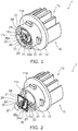
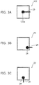
- FIGS. 1 and 2 are schematic perspective views illustrating a lighting device 1 according to the embodiment.
- Fig. 1 is a schematic perspective view of the lighting device 1
- Fig. 2 is a schematic exploded view of the lighting device 1.
- a sealing section 27 is omitted to easily read the view.
- the lighting device 1 is provided with a body section 10, a light emitting section 20, and a power supplying section 30.
- the body section 10 is provided with a housing section 11, a flange section 12, and fins 13.
- the housing section 11 has a cylindrical shape and protrudes from one surface of the flange section 12.
- the light emitting section 20 is housed inside the housing section 11.
- power supplying terminals 31 of the power supplying section 30 protrude inside the housing section 11.
- a plurality of convex sections 11a protrude on an outer surface of the housing section 11.
- the plurality of convex sections 11a hold the lighting device 1 in a lamp apparatus (not illustrated) in cooperation with a mounting member of the lamp apparatus when mounting the lighting device 1 on the lamp apparatus (not illustrated) and the like.
- a sealing member formed of a material such as rubber or silicone may be provided between the plurality of convex sections 11a and the flange section 12.
- a plurality of convex sections 11b protrude on an inner surface of the housing section 11.
- the plurality of convex sections 11b are provided to increase rigidity of the housing section 11.
- a concave section 11c is provided on the flange section 12 side on the inside of the housing section 11.
- a substrate 21 of the light emitting section 20 is mounted on the inside of the concave section 11c.
- the power supplying terminal 31 of the power supplying section 30 protrudes from a bottom surface of the concave section 11c.
- the flange section 12 has a disk shape and the housing section 11 is provided on one surface of the flange section 12, and the fins 13 are provided on the other surface of the flange section 12.
- a plurality of fins 13 are provided to protrude from the surface of the flange section 12.
- the plurality of fins 13 have a disk shape and function as radiating fins.
- the body section 10 has a function of housing the light emitting section 20, the power supplying section 30, and the like, and a function of radiating heat generated by the light emitting section 20 or the power supplying section 30 to the outside of the lighting device 1.
- the body section 10 from a material having high thermal conductivity in consideration of discharging heat to the outside.
- the body section 10 can be formed from aluminum, aluminum alloy, resin having the high thermal conductivity, and the like.
- the light emitting section 20 is provided with the substrate 21, light emitting elements 22, control elements 23, a wiring pattern 24, wiring 25, a surrounding wall member 26, and the sealing section 27.
- the substrate 21 has a plate shape and is provided with the wiring pattern 24 on a surface thereof.
- a material or a structure of the substrate 21 is not specifically limited.
- the substrate 21 can be formed of an inorganic material (ceramic) such as aluminum oxide or aluminum nitride, an organic material such as paper phenol or glass epoxy, and the like.
- the substrate 21 may be a metal plate with a surface coated by an insulator.
- the insulator may be made of an organic material or may be made of an inorganic material.
- the substrate 21 is formed using a material having the high thermal conductivity from the viewpoint of radiation.
- a material having the high thermal conductivity for example, ceramic such as aluminum oxide or aluminum nitride, resin having the high thermal conductivity, a metal plate with a surface coated by the insulator, and the like can be exemplified.
- the substrate 21 may have a single layer structure or a multi-layer structure.
- a plurality of light emitting elements 22 are mounted on the wiring pattern 24.
- the light emitting element 22 has an electrode 28 in the vicinity of one of a plurality of corner portions of a surface (upper surface) opposite to a side on which the wiring pattern 24 is provided or in the vicinity of a center portion of one of a plurality of sides of the surface (see Figs. 3(b) and 3(c) ). That is, the light emitting element 22 has one electrode 28 in the vicinity of a circumference edge of the upper surface. Detailed description of the electrode 28 will be described below.
- the electrode provided on a lower surface of the light emitting element 22 is electrically connected to a mounting pad 24c (see Fig. 7(b) ) through a conductive thermoset material such as silver paste.
- the electrode 28 provided on the upper surface of the light emitting element 22 is electrically connected to a wiring pad 24b through the wiring 25.
- the light emitting element 22 may be a light emitting diode, an organic light emitting diode, a laser diode, and the like.
- a light emitting surface of the light emitting element 22 is directed to a front side of the lighting device 1 and light is mainly emitted toward the front side of the lighting device 1.
- the number or the size of the light emitting elements 22 is not limited to the example and can be appropriately changed depending on the size or use of the lighting device 1.
- the control element 23 is mounted on the wiring pattern 24.
- the control element 23 controls a current flowing through the light emitting element 22. That is, the control element 23 controls light emitted from the light emitting element 22.
- the wiring pattern 24 is provided on at least one surface of the substrate 21.
- the wiring pattern 24 can be provided on both surfaces of the substrate 21, but it is preferable that the wiring pattern 24 is provided on one surface of the substrate 21 to reduce the manufacturing cost.
- the wiring pattern 24 is provided with an input terminal 24a, the wiring pad 24b, and the mounting pad 24c.
- a plurality of input terminals 24a are provided.
- the power supplying terminal 31 of the power supplying section 30 is electrically connected to the input terminal 24a.
- the light emitting element 22 and the control element 23 are electrically connected to the power supplying section 30 through the wiring pattern 24.
- a plurality of wiring pads 24b are provided.
- the wiring pad 24b is a portion to which one end of the wiring 25 is connected (see Fig. 7(b) ).
- the mounting pad 24c is a portion to which the light emitting element 22 is connected by using a paste-like thermoset material such as silver paste (see Fig. 7(b) ).
- the wiring 25 electrically connects the electrode 28 which is provided on the upper surface of the light emitting element 22 and the wiring pad 24b.
- the wiring 25 can be a wire which is mainly composed of gold.
- the material of the wiring 25 is not limited to the material which is mainly composed of gold and, for example, may be a material which is mainly composed of cooper or a material which is mainly composed of aluminum.
- the wiring 25 is electrically connected to the electrode 28 which is provided on the upper surface of the light emitting element 22 and the wiring pad 24b by ultrasonic welding or heat welding.
- the wiring 25 can be electrically connected to the electrode 28 which is provided on the upper surface of the light emitting element 22 and the wiring pad 24b by using a wire bonding method.
- the surrounding wall member 26 is provided to surround the plurality of light emitting elements 22.
- the surrounding wall member 26 has a circular shape and the plurality of light emitting elements 22 are exposed to a center portion 26a.
- the surrounding wall member 26 can be formed of resin, ceramic, metal such as aluminum, and the like.
- a side wall surface of the surrounding wall member 26 on the center portion 26a side is an inclined surface. Some of light emitted from the light emitting element 22 is reflected on the side wall surface of the surrounding wall member 26 on the center portion 26a side and is emitted toward the front side of the lighting device 1.
- light which is some of light emitted from the light emitting element 22 to the front side of the lighting device 1 and is totally reflected on a top surface (interface between the sealing section 27 and outside air) of the sealing section 27, is reflected on the side wall surface of the surrounding wall member 26 on the center portion 26a side and is re-emitted toward the front side of the lighting device 1.
- the surrounding wall member 26 also can have a function of a reflector. Moreover, a form of the surrounding wall member 26 is not limited to the illustrated example and can be appropriately changed.
- the sealing section 27 is provided in the center portion 26a of the surrounding wall member 26.
- the sealing section 27 is provided to cover the inside of the surrounding wall member 26.
- the sealing section 27 is formed of a material having a light-transmitting property.
- the sealing section 27 can be formed of a silicone resin.
- the sealing section 27 can be formed by filling the center portion 26a of the surrounding wall member 26 with resin.
- filling with resin can be performed by using a liquid fixed-quantity discharge device such as a dispenser.
- the center portion 26a of the surrounding wall member 26 is filled with resin, it is possible to suppress mechanical contact from outside to the light emitting element 22, the wiring pattern 24, and the wiring 25 which are exposed to the center portion 26a of the surrounding wall member 26. Furthermore, it is possible to suppress attaching of air, moisture, and the like to the light emitting element 22, the wiring pattern 24, and the wiring 25 which are exposed to the center portion 26a of the surrounding wall member 26. Thus, it is possible to increase reliability of the lighting device 1.
- the center portion 26a of the surrounding wall member 26 is filled with resin, it is possible to decrease a difference in refractive index between the light emitting element 22 and the outside of the light emitting element 22. Thus, it is possible to suppress that some of light emitted from a light emitting layer (not illustrated) of the light emitting element 22 is totally reflected on the interface between the upper surface of the light emitting element 22 and the resin filling the center portion 26a.
- the sealing section 27 may include a phosphor.
- the phosphor can be a YAG phosphor (yttrium-aluminum-garnet phosphor).
- the light emitting element 22 is a blue light emitting diode and the phosphor is the YAG phosphor
- the YAG phosphor is excited by blue light emitted from the light emitting element 22 and yellow fluorescence is emitted from the YAG phosphor. Then, blue light and yellow light are mixed, and thereby white light is emitted from the lighting device 1.
- the type of the phosphor or the type of the light emitting element 22 is not limited to the illustrated example and can be appropriately changed so as to obtain a desired emission color depending on use and the like of the lighting device 1.
- the power supplying section 30 is provided with a plurality of power supplying terminals 31.
- Plurality of power supplying terminals 31 extend inside the housing section 11 and the flange section 12.
- One end portion of each of plurality of power supplying terminals 31 protrudes from a bottom surface of the concave section 11c of the housing section 11 and is electrically connected to the input terminal 24a of the wiring pattern 24.
- the other end portion of each of the plurality of power supplying terminals 31 is exposed from the opposite side of a side of the body section 10 on which the substrate 21 is provided.
- the number, an arrangement, and a form of the power supplying terminal 31 are not limited to the illustrated example and can be appropriately changed.
- the power supplying section 30 may include a substrate (not illustrated) or a circuit component such as a capacitor and a resistance.
- the substrate (not illustrated) or the circuit component may be provided inside the housing section 11 or the flange section 12.
- a socket (not illustrated) and the like can be appropriately provided to electrically connect the power supplying terminal 31 to an external power supply and the like.
- the socket (not illustrated) and the like may be provided on a side of the flange section 12 on which the fins 13 are provided.
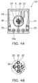
- Fig. 3 is a schematic view illustrating the position of the electrode provided on the upper surface of the light emitting element 22.
- Fig. 3(a) is a schematic view illustrating a position of an electrode 128 provided on the upper surface of a light emitting element 122 according to a comparative example.
- Figs. 3(b) and 3(c) are schematic views illustrating a position of the electrode 28 provided on the upper surface of the light emitting element 22 according to the embodiment.
- Fig. 3(a) shows a configuration in which the electrode 128 is provided in a center portion of an upper surface of a light emitting element 122. If the electrode 128 is provided in the center portion of the upper surface of the light emitting element 122, it is possible to connect the wiring 25 of equal length to the electrode 128 from any direction. However, if the electrode 128 is provided in the center portion of the upper surface of the light emitting element 122, a distance in which the wiring 25 crosses above the upper surface of the light emitting element 122 which is the light emitting surface is increased. Thus, light emitted from the light emitting element 122 is blocked by the wiring 25 and there is a concern that the light extraction efficiency is deteriorated.
- the electrode 28 is provided in the vicinity of one of a plurality of corner portions of the upper surface of the light emitting element 22.
- the electrode 28 may be provided in the vicinity of the center portion of one of a plurality of sides of the upper surface of the light emitting element 22.
- the position of the electrode 28 can be appropriately changed. That is, one electrode 28 may be provided in the vicinity of a circumference edge of the upper surface of the light emitting element 22.
- the electrode 28 is provided in the vicinity of one of the plurality of corner portions of the upper surface of the light emitting element 22 or in the vicinity of the center portion of one of the plurality of sides of the upper surface of the light emitting element 22, directionality is generated when mounting the light emitting element 22.
- the plurality of light emitting elements 22 are mounted on the substrate 21 such that the electrodes 28 of the plurality of light emitting elements 22 have the same direction, it is possible to reduce the cost in a mounting process.
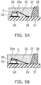
- Figs. 4(a) and 4(b) are schematic views illustrating a mounting form of a light emitting element 22 according to a comparative example.
- Fig. 4 (a) is a schematic view illustrating the mounting form in a light emitting section 120 according to the comparative example.
- Fig. 4(b) is an enlarged view of an A portion in Fig. 4(a) .
- Figs. 5(a) and 5(b) are schematic views illustrating a connection state of the wiring 25.
- the distance in which the wiring 25 crosses above the upper surface of the light emitting element 22 which is the light emitting surface may be increased.
- the heat stress, the expansion, and the contraction are generated in the sealing section 27 by turning on and turning off of the light emitting element 22.
- the volume of the sealing section 27 is increased, influences of the heat stress, the expansion, and the contraction are increased and there is a concern that defects occur in a part of the plurality of light emitting elements 22 and the wiring 25 which are sealed by the sealing section 27.
- the light emitting element 22 is separated from the substrate 21 or the wiring 25 is disconnected.
- Figs. 6(a) and 6(b) are schematic views illustrating a relationship of the connection state between a wiring pattern 224 and the wiring 25 according to the comparative example.
- Fig. 6(a) is a schematic view illustrating a mounting form in a light emitting section 220 on which the wiring pattern 224 is provided according to the comparative example.
- Fig. 6 (b) is an enlarged view of a C portion in Fig. 6 (a) .
- the plurality of light emitting elements 22 are mounted on the substrate 21 such that the electrodes 28 of the plurality of light emitting elements 22 have the same direction.
- the distance in which the wiring 25 crosses above the upper surface of the light emitting element 22 is decreased by changing the wiring pattern 224.
- an occupied region (region D2 in Fig. 6(b) ) is greater than an occupied region (region D1 in Fig. 6(b) ) in Fig. 5(b) .
- the volume of the sealing section 27 is increased as the size of a surrounding wall member 226 is increased.
- a case where the electrode 28 is provided in the vicinity of the center portion of one of the plurality of sides of the upper surface can be similar to the following case. That is, a case where one electrode 28 is provided in the vicinity of the circumference edge of the upper surface of the light emitting element 22 can be similar to the following case.
- Figs. 7(a) and 7(b) are schematic views illustrating a mounting form of the light emitting element 22 according to the embodiment.
- Fig. 7 (a) is a schematic view illustrating the mounting form of the light emitting element 22 in the light emitting section 20.
- Fig. 7 (b) is an enlarged view of a E portion in Fig. 7(a) .
- the light emitting section 20 illustrated in Figs. 7(a) and 7(b) is provided with four light emitting elements 22 centered on one light emitting element 22 in directions perpendicular to each other. Furthermore, a distance from a center of the light emitting element 22 provided in the center to a center of each light emitting element 22 provided in the circumference is equal to each other.
- the light emitting section 20 has one light emitting element 22 provided in a first position 29 and four light emitting elements 22 provided at the same distribution on the circumference (on circumference of a virtual circle 40) centered on the first position 29.
- positions of the respective electrodes 28 have the rotational symmetry centered on the first position 29 in the electric connection between the light emitting element 22 and the light emitting element 22 in the plurality of light emitting elements 22 which are connected in series.
- positions of the respective electrodes 28 have the rotational symmetry centered on the first position 29 in the electric connection between a light emitting element 22a and the light emitting element 22a in three light emitting elements 22a in Fig. 7(b) .
- each of the electrodes 28 is provided inside the virtual circle 40.
- a plurality of electrodes 28 are respectively positioned inside the circumference passing through the centers of the plurality of light emitting elements 22a connected in series centered on the first position 29 in the electric connection between the light emitting element 22a and the light emitting element 22a in the plurality of light emitting elements connected in series.
- the virtual circle 40 is a circle passing through the center of each light emitting element 22a centered on the first position 29.
- the first position 29 on the substrate 21 can be an arbitrary position.
- the center of the substrate 21 is the first position 29.
- five light emitting elements 22 and 22a are provided in positions in which distances between the plurality of wiring pads 24b and the plurality of electrodes 28 are respectively the shortest.
- connection position between the wiring 25 and the wiring pattern 24 can be close to the first position 29.
- the size of the surrounding wall member 26 can be decreased and the volume of the sealing section 27 can be decreased.
- the surrounding wall member 26 is provided in the lighting device 1, it is possible to regulate the volume (capacity for being filled (injected) with resin and the like) of the sealing section 27 to a small capacity (small range). Thus, it is possible to suppress stress, expansion, and contraction of the sealing section 27 to be lower than a sealing section having a large capacity. As a result, it is possible to suppress influences on a part of the plurality of light emitting elements 22 and the wirings 25 sealed by the sealing section 27, for example, separation of the light emitting element 22 or disconnection of the wiring 25.
- the volume of the sealing section 27 has a small capacity, it is possible to suppress occurrence of cracks of the sealing section 27 to be lower than that of the sealing section having a large capacity. As a result, sealing performance of the sealing section 27 can be improved, and it is possible to improve a yield of manufacture of the lighting device 1.
- the volume of the sealing section 27 is the small capacity, it is possible to reduce the manufacturing cost. Furthermore, since a time for filling the sealing section 27 can be reduced, it is possible to shorten a manufacturing time and reduce the manufacturing cost.
- Figs. 8(a) and 8(b) are schematic views illustrating a mounting form of the light emitting element 22 according to another embodiment.
- Fig. 8 (a) is a schematic view illustrating the mounting form of the light emitting element 22 in a light emitting section 20a.
- Fig. 8 (b) is an enlarged view of a F portion in Fig. 8(a) .
- the light emitting section 20a illustrated in Figs. 8 (a) and 8(b) is provided with four light emitting elements 22 centered on the first position 29 in directions perpendicular to each other. Furthermore, a distance from the first position 29 to a center of each light emitting element 22 is equal to each other.
- the light emitting section 20 has four light emitting elements 22 provided at the same distribution on the circumference (on circumference of the virtual circle 40) centered on the first position 29.
- the four light emitting elements 22 are connected in series.
- positions of the respective electrodes 28 have the rotational symmetry centered on the first position 29 in the electric connection between the light emitting element 22 and the light emitting element 22 in the plurality of light emitting elements 22 which are connected in series.
- positions of the respective electrodes 28 have the rotational symmetry centered on the first position 29 in the electric connection between the light emitting element 22a and the light emitting element 22a in three light emitting elements 22a in Fig. 8(b) .
- the light emitting elements 22 (22a) in Fig. 8(b) are a case where the light emitting elements 22 (22a) provided on the circumference in Fig. 7(b) are respectively rotated approximately 45° with respect to the center of the light emitting element 22 (22a).
- the plurality of electrodes 28 are respectively positioned on the circumference passing through the centers of the plurality of light emitting elements 22a which are connected in series centered on the first position 29 in the electric connection between the light emitting element 22a and the light emitting element 22a in the plurality of light emitting elements which are connected in series.
- four light emitting elements 22 and 22a are provided in positions in which distances between the plurality of wiring pads 24b and the plurality of electrodes 28 are respectively the shortest.
- Figs. 9(a) and 9(b) are schematic views illustrating a mounting form of a light emitting element 22 according to another embodiment.
- Fig. 9 (a) is a schematic view illustrating the mounting form of the light emitting element 22 in a light emitting section 20b.
- Fig. 9 (b) is an enlarged view of a G portion in Fig. 9(a) .
- the light emitting section 20b illustrated in Figs. 9 (a) and 9(b) is provided with four light emitting elements 22 respectively centered on one light emitting element 22 in directions perpendicular to each other.
- each light emitting element 22 and each electrode 28 in the light emitting section 20b is similar to the arrangement form of each light emitting element 22 and each electrode 28 in the light emitting section 20 illustrated in Figs. 7(a) and 7(b) .
- the plurality of electrodes 28 are respectively positioned inside the circumference passing through the centers of the plurality of light emitting elements 22a which are connected in series centered on the first position 29 in the electric connection between the light emitting element 22a and the light emitting element 22a in the plurality of light emitting elements which are connected in series.
- a connection portion between the wiring pad 24b and the wiring 25, and the mounting pad 24c are provided inside a virtual circle 41 passing through the outermost peripheral end of the mounting pads 24c centered on the first position 29.
- five light emitting elements 22 and 22a are provided in positions in which distances between the plurality of wiring pads 24b and the plurality of electrodes 28 are respectively the shortest.
- Figs. 10(a) and 10(b) are schematic views illustrating a mounting form of a light emitting element 22 according to another embodiment.
- Fig. 10(a) is a schematic view illustrating the mounting form of the light emitting element 22 in a light emitting section 20c.
- Fig. 10(b) is an enlarged view of a H portion in Fig. 10(a) .
- the light emitting section 20c has six light emitting elements 22 provided at the same distribution on the circumference (on circumference of the virtual circle 40) centered on the first position 29.
- the six light emitting elements 22 are connected in series.
- the electrodes 28 are respectively provided inside the virtual circle 40 in the electric connection between the light emitting element 22 and the light emitting element 22 in the plurality of light emitting elements which are connected in series.
- six light emitting elements 22 and 22a are provided in positions in which distances between the plurality of wiring pads 24b and the plurality of electrodes 28 are respectively the shortest.
- the plurality of electrodes 28 are respectively positioned inside the circumference passing through the centers of the plurality of light emitting elements 22 which are connected in series centered on the first position 29 in the electric connection between the light emitting element 22 and the light emitting element 22 in the plurality of light emitting elements which are connected in series.
- Figs. 11(a) and 11(b) are schematic views illustrating a mounting form of a light emitting element 22 according to another embodiment.
- Fig. 11(a) is a schematic view illustrating the mounting form of the light emitting element 22 in a light emitting section 20d.
- Fig. 11(b) is an enlarged view of an I portion in Fig. 11(a) .
- the light emitting section 20d has eight light emitting elements 22 provided at the same distribution on the circumference (on circumference of the virtual circle 40) centered on the first position 29.
- the electrodes 28 are respectively provided inside the virtual circle 40 in the electric connection between the light emitting element 22a1 and the light emitting element 22a1 in the four light emitting elements 22a1 which are connected in series.
- the electrodes 28 are respectively provided inside the virtual circle 40 in the electric connection between the light emitting element 22a2 and the light emitting element 22a2 in the four light emitting elements 22a2 which are connected in series.
- positions of the respective electrodes 28 have the rotational symmetry centered on the first position 29 in the electric connection between the light emitting element 22a1 and the light emitting element 22a1 in the four light emitting elements 22a1 which are connected in series.
- positions of the respective electrodes 28 have the rotational symmetry centered on the first position 29 in the electric connection between the light emitting element 22a2 and the light emitting element 22a2 in the four light emitting elements 22a2 which are connected in series.
- eight light emitting elements 22 and 22a are provided in positions in which distances between the plurality of wiring pads 24b and the plurality of electrodes 28 are respectively the shortest.
- the plurality of electrodes 28 are respectively positioned inside the circumference passing through the centers of the plurality of light emitting elements 22a1 and 22a2 which are connected in series centered on the first position 29 in the electric connection between the light emitting elements 22a1 and 22a2, and the light emitting elements 22a1 and 22a2 in the plurality of light emitting elements 22a1 and 22a2 which are connected in series.
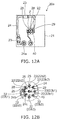
- Figs. 12(a) and 12(b) are schematic views illustrating a mounting form of a light emitting element 22 according to another embodiment.
- Fig. 12(a) is a schematic view illustrating the mounting form of the light emitting element 22 in a light emitting section 20e.
- Fig. 12(b) is an enlarged view of a J portion in Fig. 12(a) .
- the light emitting section 20e has one light emitting element 22b1 provided in the first position 29 and eight light emitting elements 22b1, 22b2, and 22b3 provided at the same distribution on the circumference (on circumference of the virtual circle 40) centered on the first position 29.
- three light emitting elements 22b1 which are connected in series, three light emitting elements 22b2 which are connected in series, and three light emitting elements 22b3 which are connected in series are connected in parallel.
- the electrodes 28 are respectively provided inside the virtual circle 40 in the electric connection between the light emitting element 22b1 and the light emitting element 22b1 in the three light emitting elements 22b1 which are connected in series.
- the electrodes 28 are respectively provided inside the virtual circle 40 in the electric connection between the light emitting element 22b2 and the light emitting element 22b2 in the three light emitting elements 22b2 which are connected in series.
- the electrodes 28 are respectively provided inside the virtual circle 40 in the electric connection between the light emitting element 22b3 and the light emitting element 22b3 in the three light emitting elements 22b3 which are connected in series.
- positions of the respective electrodes 28 have the rotational symmetry centered on the first position 29 in the electric connection between the light emitting element 22b2 and the light emitting element 22b2 in the three light emitting elements 22b2 which are connected in series.
- positions of the respective electrodes 28 have the rotational symmetry centered on the first position 29 in the electric connection between the light emitting element 22b3 and the light emitting element 22b3 in the three light emitting elements 22b3 which are connected in series.
- nine light emitting elements 22b1, 22b2, and 22b3 are provided in positions in which distances between the plurality of wiring pads 24b and the plurality of electrodes 28 are respectively the shortest.
- the plurality of electrodes 28 are respectively positioned inside the circumference passing through the centers of the plurality of light emitting elements 22b2 and 22b3 which are connected in series centered on the first position 29 in the electric connection between the light emitting elements 22b2 and 22b3, and the light emitting elements 22b2 and 22b3 in the plurality of light emitting elements 22b2 and 22b3 which are connected in series.
- Figs. 13(a) and 13(b) are schematic views illustrating a mounting form of a light emitting element 22 according to another embodiment.
- Fig. 13(a) is a schematic view illustrating the mounting form of the light emitting element 22 in a light emitting section 20f.
- Fig. 13(b) is an enlarged view of a K portion in Fig. 13(a) .
- the light emitting section 20f has two light emitting element 22c1 provided to interpose the first position 29 and ten light emitting elements 22c1, 22c2, and 22c3 provided in the same distribution on the circumference (on circumference of the virtual circle 40) centered on the first position 29.
- the electrodes 28 are respectively provided inside the virtual circle 40 in the electric connection between the light emitting element 22c1 and the light emitting element 22c1 in the four light emitting elements 22c1 which are connected in series.
- the electrodes 28 are respectively provided inside the virtual circle 40 in the electric connection between the light emitting element 22c2 and the light emitting element 22c2 in the four light emitting elements 22c2 which are connected in series.
- the electrodes 28 are respectively provided inside the virtual circle 40 in the electric connection between the light emitting element 22c3 and the light emitting element 22c3 in the four light emitting elements 22c3 which are connected in series.
- twelve light emitting elements 22c1, 22c2, and 22c3 are provided in positions in which distances between the plurality of wiring pads 24b and the plurality of electrodes 28 are respectively the shortest.
- the plurality of electrodes 28 are respectively positioned inside the circumference passing through the centers of the plurality of light emitting elements 22c2 and 22c3 which are connected in series centered on the first position 29 in the electric connection between the light emitting elements 22c2 and 22c3, and the light emitting elements 22c2 and 22c3 in the plurality of light emitting elements 22c2 and 22c3 which are connected in series.
Landscapes
- Engineering & Computer Science (AREA)
- Physics & Mathematics (AREA)
- Microelectronics & Electronic Packaging (AREA)
- Optics & Photonics (AREA)
- General Engineering & Computer Science (AREA)
- Led Device Packages (AREA)
- Non-Portable Lighting Devices Or Systems Thereof (AREA)
Abstract
Description
- Embodiments described herein generally relate to a lighting device.
- There is a lighting device having a plurality of light emitting elements such as Light Emitting Diode (LED).
- In the lighting device having the plurality of light emitting elements, the plurality of light emitting elements are arranged on circumference on a substrate or the plurality of light emitting elements are arranged in an array shape (vertical and horizontal arrangement).
- Furthermore, the light emitting elements and a wiring pattern on a surface of the substrate are electrically connected by wiring.
- Then, the plurality of light emitting elements arranged as described above and the wiring are sealed by a resin molded section, that is, by a sealing section.
- Here, heat stress, expansion, and contraction are generated in the sealing section by turning on and turning off of the light emitting elements. In this case, if the volume of the sealing section is great, influences of the heat stress, the expansion, and the contraction of the sealing section are large, and there is a concern that defects occur in a part of the plurality of light emitting elements and a plurality of wirings sealed by the sealing section.
- For example, there is a concern that the light emitting elements are separated from the substrate or the wiring is disconnected.
- Thus, it is preferable that the volume of the sealing section is small as much as possible.
- However, if the plurality of light emitting elements are regularly arranged on the substrate and the plurality of light emitting elements which are regularly arranged are simply sealed by the sealing section, there is a concern that the volume of the sealing section is increased.
- Furthermore, a distance in which wiring crosses above an upper surface of the light emitting element which is a light emitting surface is increased, emitted light is blocked by the wiring, and thus there is a concern that light extraction efficiency is deteriorated.
-
- [PTL 1]
JP-A-2007-176219 - [PTL 2]
JP-A-2009-21264 - An object of the invention is to provide a lighting device in which the volume of a sealing section can be decreased and a light extraction efficiency can be improved.
- A lighting device according to an embodiment includes a body section; a substrate that is provided in the body section; a wiring pattern that is provided on a surface of the substrate and has a plurality of wiring pads; a plurality of light emitting elements that are provided on the wiring pattern and have electrodes in the vicinity of a the circumference edge of a surface opposite to a side on which the wiring pattern is provided; a plurality of wirings that respectively connect the plurality of wiring pads and a plurality of electrodes; a surrounding wall member that is provided so as to surround the plurality of light emitting elements and has an annular shape; and a sealing section that is provided so as to cover the inside of the surrounding wall member.
- Then, at least a part of the plurality of light emitting elements is connected in series. The plurality of electrodes are respectively positioned on or inside a circumference passing through centers of the plurality of light emitting elements which are connected in series centered on a first position in electric connection between the light emitting element and the light emitting element in the plurality of light emitting elements connected in series.
- According to the embodiments of the invention, it is possible to provide a lighting device in which the volume of a sealing section can be decreased and a light extraction efficiency can be improved.
-
-
Fig. 1 is a schematic perspective view illustrating a lighting device according to an embodiment. -
Fig. 2 is a schematic perspective view illustrating the lighting device according to the embodiment. -
Fig. 3(a) is a schematic view illustrating a position of an electrode provided on an upper surface of a light emitting element according to a comparative example andFigs. 3(b) and 3(c) are schematic views illustrating a position of an electrode provided on an upper surface of a light emitting element according to the embodiment. -
Figs. 4(a) and 4(b) are schematic views illustrating a mounting form of the light emitting element according to a comparative example. -
Figs. 5(a) and 5(b) are schematic views illustrating a connection state of wiring. -
Figs. 6(a) and 6(b) are schematic views illustrating a relationship of a connection state between a wiring pattern and wiring according to the comparative example. -
Figs. 7(a) and 7(b) are schematic views illustrating a mounting form of the light emitting element according to the embodiment. -
Figs. 8(a) and 8(b) are schematic views illustrating a mounting form of a light emitting element according to another embodiment. -
Figs. 9(a) and 9(b) are schematic views illustrating a mounting form of a light emitting element according to another embodiment. -
Figs. 10(a) and 10(b) are schematic views illustrating a mounting form of a light emitting element according to another embodiment. -
Figs. 11(a) and 11(b) are schematic views illustrating a mounting form of a light emitting element according to another embodiment. -
Figs. 12(a) and 12(b) are schematic views illustrating a mounting form of a light emitting element according to another embodiment. -
Figs. 13(a) and 13(b) are schematic views illustrating a mounting form of a light emitting element according to another embodiment. - A first invention is a lighting device including a body section; a substrate that is provided in the body section; a wiring pattern that is provided on a surface of the substrate and has a plurality of wiring pads; a plurality of light emitting elements that are provided on the wiring pattern and have electrodes in the vicinity of a the circumference edge of a surface opposite to a side on which the wiring pattern is provided; a plurality of wirings that respectively connect the plurality of wiring pads and a plurality of electrodes; a surrounding wall member that is provided so as to surround the plurality of light emitting elements and has an annular shape; and a sealing section that is provided so as to cover the inside of the surrounding wall member.
- Then, at least a part of the plurality of light emitting elements is connected in series. The plurality of electrodes are respectively positioned on or inside a circumference passing through centers of the plurality of light emitting elements which are connected in series centered on a first position in electric connection between the light emitting element and the light emitting element in the plurality of light emitting elements connected in series.
- In the lighting device, it is possible to make the connection portion between the wiring and the wiring pattern (wiring pad) be close to the vicinity of the first position. Thus, it is possible to decrease a size of the surrounding wall member and to decrease the volume of the sealing section.
- Furthermore, it is possible to shorten a distance in which the wiring crosses above an upper surface of the light emitting element which is a light emitting surface and to improve light extraction efficiency.
- Furthermore, since the surrounding wall member is provided in the lighting device, it is possible to regulate the volume (capacity for being filled (injected) with resin and the like) of the sealing section to a small capacity (small range). Thus, it is possible to suppress stress, expansion, and contraction of the sealing section to be lower than a sealing section having a large capacity. As a result, it is possible to suppress influences on a part of the plurality of light emitting elements and the wirings sealed by the sealing section, for example, separation of the light emitting element or disconnection of the wiring.
- Furthermore, in the lighting device, since the volume of the sealing section has a small capacity, it is possible to suppress occurrence of cracks of the sealing section to be lower than that of the sealing section having a large capacity. As a result, sealing performance of the sealing section can be improved, and thus it is possible to improve a yield of manufacture of the lighting device.
- Furthermore, in the lighting device, since the volume of the sealing section is the small capacity, it is possible to reduce manufacturing cost. Furthermore, a time for filling the sealing section can be reduced, and thus it is possible to shorten a manufacturing time and reduce the manufacturing cost.
- In a second invention according to the first invention, positions of the respective electrodes have a rotational symmetry centered on the first position in the electric connection between the light emitting element and the light emitting element in the plurality of light emitting elements connected in series.
- In the lighting device, it is possible to further decrease the volume of the sealing section and to improve the light extraction efficiency.
- In a third invention according to the first or second invention, the plurality of light emitting elements are respectively provided in positions where distances between the plurality of wiring pads and the plurality of electrodes respectively become the shortest.
- In the lighting device, it is possible to further decrease the volume of the sealing section and to improve the light extraction efficiency.
- In a fourth invention according to any one of the first to third inventions, the wiring pattern has a plurality of mounting pads to which the plurality of light emitting elements are respectively connected. Then, the plurality of electrodes, and connection portions between the wiring pads and the wirings are positioned inside circumference passing through outermost circumference end of the plurality of mounting pads centered on the first position.
- In the lighting device, it is possible to further decrease the volume of the sealing section and to improve the light extraction efficiency.
- In a fifth invention according to any one of the first to fourth inventions, the lighting device further includes a power supplying terminal of which one end is electrically connected to the wiring pattern and the other end is exposed from the opposite side of a side of the body section on which the substrate is provided.
- Hereinafter, embodiments will be illustrated with reference to the drawings. Moreover, in each view, the same reference numerals are given to the same configuration elements and detailed description will be appropriately omitted.
Figs. 1 and 2 are schematic perspective views illustrating alighting device 1 according to the embodiment. - Moreover,
Fig. 1 is a schematic perspective view of thelighting device 1 andFig. 2 is a schematic exploded view of thelighting device 1. - In addition, in
Fig. 1 , asealing section 27 is omitted to easily read the view. - As illustrated in
Figs. 1 and 2 , thelighting device 1 is provided with abody section 10, alight emitting section 20, and apower supplying section 30. - The
body section 10 is provided with ahousing section 11, aflange section 12, andfins 13. Thehousing section 11 has a cylindrical shape and protrudes from one surface of theflange section 12. Thelight emitting section 20 is housed inside thehousing section 11. In addition,power supplying terminals 31 of thepower supplying section 30 protrude inside thehousing section 11. - A plurality of
convex sections 11a protrude on an outer surface of thehousing section 11. For example, the plurality ofconvex sections 11a hold thelighting device 1 in a lamp apparatus (not illustrated) in cooperation with a mounting member of the lamp apparatus when mounting thelighting device 1 on the lamp apparatus (not illustrated) and the like. - In addition, a sealing member formed of a material such as rubber or silicone may be provided between the plurality of
convex sections 11a and theflange section 12. - A plurality of
convex sections 11b protrude on an inner surface of thehousing section 11. The plurality ofconvex sections 11b are provided to increase rigidity of thehousing section 11. - A
concave section 11c is provided on theflange section 12 side on the inside of thehousing section 11. Asubstrate 21 of thelight emitting section 20 is mounted on the inside of theconcave section 11c. In addition, thepower supplying terminal 31 of thepower supplying section 30 protrudes from a bottom surface of theconcave section 11c. - The
flange section 12 has a disk shape and thehousing section 11 is provided on one surface of theflange section 12, and thefins 13 are provided on the other surface of theflange section 12. - A plurality of
fins 13 are provided to protrude from the surface of theflange section 12. The plurality offins 13 have a disk shape and function as radiating fins. - The
body section 10 has a function of housing thelight emitting section 20, thepower supplying section 30, and the like, and a function of radiating heat generated by thelight emitting section 20 or thepower supplying section 30 to the outside of thelighting device 1. - Thus, it is possible to form the
body section 10 from a material having high thermal conductivity in consideration of discharging heat to the outside. For example, thebody section 10 can be formed from aluminum, aluminum alloy, resin having the high thermal conductivity, and the like. - In this case, it is possible to form a portion such as the
fins 13 from which heat is discharged to the outside from a material having the high thermal conductivity and to form the other portions from resin and the like. - The
light emitting section 20 is provided with thesubstrate 21,light emitting elements 22,control elements 23, awiring pattern 24, wiring 25, a surroundingwall member 26, and the sealingsection 27. - The
substrate 21 has a plate shape and is provided with thewiring pattern 24 on a surface thereof. - A material or a structure of the
substrate 21 is not specifically limited. For example, thesubstrate 21 can be formed of an inorganic material (ceramic) such as aluminum oxide or aluminum nitride, an organic material such as paper phenol or glass epoxy, and the like. In addition, thesubstrate 21 may be a metal plate with a surface coated by an insulator. Moreover, if the surface of the metal plate is coated by the insulator, the insulator may be made of an organic material or may be made of an inorganic material. - In this case, if a heat generation amount of the
light emitting element 22 is great, it is preferable that thesubstrate 21 is formed using a material having the high thermal conductivity from the viewpoint of radiation. As the material having the high thermal conductivity, for example, ceramic such as aluminum oxide or aluminum nitride, resin having the high thermal conductivity, a metal plate with a surface coated by the insulator, and the like can be exemplified. - Furthermore, the
substrate 21 may have a single layer structure or a multi-layer structure. - A plurality of
light emitting elements 22 are mounted on thewiring pattern 24. - The
light emitting element 22 has anelectrode 28 in the vicinity of one of a plurality of corner portions of a surface (upper surface) opposite to a side on which thewiring pattern 24 is provided or in the vicinity of a center portion of one of a plurality of sides of the surface (seeFigs. 3(b) and 3(c) ). That is, thelight emitting element 22 has oneelectrode 28 in the vicinity of a circumference edge of the upper surface. Detailed description of theelectrode 28 will be described below. - The electrode provided on a lower surface of the
light emitting element 22 is electrically connected to amounting pad 24c (seeFig. 7(b) ) through a conductive thermoset material such as silver paste. Theelectrode 28 provided on the upper surface of thelight emitting element 22 is electrically connected to awiring pad 24b through thewiring 25. - For example, the
light emitting element 22 may be a light emitting diode, an organic light emitting diode, a laser diode, and the like. - A light emitting surface of the
light emitting element 22 is directed to a front side of thelighting device 1 and light is mainly emitted toward the front side of thelighting device 1. - The number or the size of the
light emitting elements 22 is not limited to the example and can be appropriately changed depending on the size or use of thelighting device 1. - Moreover, detailed description regarding embodiments of the
light emitting element 22 will be described below. - The
control element 23 is mounted on thewiring pattern 24. - The
control element 23 controls a current flowing through thelight emitting element 22. That is, thecontrol element 23 controls light emitted from thelight emitting element 22. - The
wiring pattern 24 is provided on at least one surface of thesubstrate 21. - The
wiring pattern 24 can be provided on both surfaces of thesubstrate 21, but it is preferable that thewiring pattern 24 is provided on one surface of thesubstrate 21 to reduce the manufacturing cost. - The
wiring pattern 24 is provided with aninput terminal 24a, thewiring pad 24b, and the mountingpad 24c. - A plurality of
input terminals 24a are provided. Thepower supplying terminal 31 of thepower supplying section 30 is electrically connected to theinput terminal 24a. Thus, thelight emitting element 22 and thecontrol element 23 are electrically connected to thepower supplying section 30 through thewiring pattern 24. - A plurality of
wiring pads 24b are provided. Thewiring pad 24b is a portion to which one end of thewiring 25 is connected (seeFig. 7(b) ). - A plurality of mounting
pads 24c are provided. The mountingpad 24c is a portion to which thelight emitting element 22 is connected by using a paste-like thermoset material such as silver paste (seeFig. 7(b) ). - The
wiring 25 electrically connects theelectrode 28 which is provided on the upper surface of thelight emitting element 22 and thewiring pad 24b. For example, thewiring 25 can be a wire which is mainly composed of gold. However, the material of thewiring 25 is not limited to the material which is mainly composed of gold and, for example, may be a material which is mainly composed of cooper or a material which is mainly composed of aluminum. - For example, the
wiring 25 is electrically connected to theelectrode 28 which is provided on the upper surface of thelight emitting element 22 and thewiring pad 24b by ultrasonic welding or heat welding. For example, thewiring 25 can be electrically connected to theelectrode 28 which is provided on the upper surface of thelight emitting element 22 and thewiring pad 24b by using a wire bonding method. - The surrounding
wall member 26 is provided to surround the plurality oflight emitting elements 22. For example, the surroundingwall member 26 has a circular shape and the plurality oflight emitting elements 22 are exposed to acenter portion 26a. - For example, the surrounding
wall member 26 can be formed of resin, ceramic, metal such as aluminum, and the like. - A side wall surface of the surrounding
wall member 26 on thecenter portion 26a side is an inclined surface. Some of light emitted from thelight emitting element 22 is reflected on the side wall surface of the surroundingwall member 26 on thecenter portion 26a side and is emitted toward the front side of thelighting device 1. - In addition, light, which is some of light emitted from the
light emitting element 22 to the front side of thelighting device 1 and is totally reflected on a top surface (interface between the sealingsection 27 and outside air) of the sealingsection 27, is reflected on the side wall surface of the surroundingwall member 26 on thecenter portion 26a side and is re-emitted toward the front side of thelighting device 1. - That is, the surrounding
wall member 26 also can have a function of a reflector. Moreover, a form of the surroundingwall member 26 is not limited to the illustrated example and can be appropriately changed. - The sealing
section 27 is provided in thecenter portion 26a of the surroundingwall member 26. The sealingsection 27 is provided to cover the inside of the surroundingwall member 26. - The sealing
section 27 is formed of a material having a light-transmitting property. For example, the sealingsection 27 can be formed of a silicone resin. - For example, the sealing
section 27 can be formed by filling thecenter portion 26a of the surroundingwall member 26 with resin. For example, filling with resin can be performed by using a liquid fixed-quantity discharge device such as a dispenser. - If the
center portion 26a of the surroundingwall member 26 is filled with resin, it is possible to suppress mechanical contact from outside to thelight emitting element 22, thewiring pattern 24, and thewiring 25 which are exposed to thecenter portion 26a of the surroundingwall member 26. Furthermore, it is possible to suppress attaching of air, moisture, and the like to thelight emitting element 22, thewiring pattern 24, and thewiring 25 which are exposed to thecenter portion 26a of the surroundingwall member 26. Thus, it is possible to increase reliability of thelighting device 1. - In addition, if the
center portion 26a of the surroundingwall member 26 is filled with resin, it is possible to decrease a difference in refractive index between the light emittingelement 22 and the outside of thelight emitting element 22. Thus, it is possible to suppress that some of light emitted from a light emitting layer (not illustrated) of thelight emitting element 22 is totally reflected on the interface between the upper surface of thelight emitting element 22 and the resin filling thecenter portion 26a. - In addition, the sealing
section 27 may include a phosphor. For example, the phosphor can be a YAG phosphor (yttrium-aluminum-garnet phosphor). - For example, if the
light emitting element 22 is a blue light emitting diode and the phosphor is the YAG phosphor, the YAG phosphor is excited by blue light emitted from thelight emitting element 22 and yellow fluorescence is emitted from the YAG phosphor. Then, blue light and yellow light are mixed, and thereby white light is emitted from thelighting device 1. Moreover, the type of the phosphor or the type of thelight emitting element 22 is not limited to the illustrated example and can be appropriately changed so as to obtain a desired emission color depending on use and the like of thelighting device 1. - The
power supplying section 30 is provided with a plurality ofpower supplying terminals 31. Plurality ofpower supplying terminals 31 extend inside thehousing section 11 and theflange section 12. One end portion of each of plurality ofpower supplying terminals 31 protrudes from a bottom surface of theconcave section 11c of thehousing section 11 and is electrically connected to theinput terminal 24a of thewiring pattern 24. The other end portion of each of the plurality ofpower supplying terminals 31 is exposed from the opposite side of a side of thebody section 10 on which thesubstrate 21 is provided. - Moreover, the number, an arrangement, and a form of the
power supplying terminal 31 are not limited to the illustrated example and can be appropriately changed. - In addition, the
power supplying section 30 may include a substrate (not illustrated) or a circuit component such as a capacitor and a resistance. Moreover, for example, the substrate (not illustrated) or the circuit component may be provided inside thehousing section 11 or theflange section 12. - Additionally, a socket (not illustrated) and the like can be appropriately provided to electrically connect the
power supplying terminal 31 to an external power supply and the like. Moreover, for example, the socket (not illustrated) and the like may be provided on a side of theflange section 12 on which thefins 13 are provided. - Next, the embodiment of the
light emitting element 22 will be further described. - First, a position of the
electrode 28 provided on the upper surface of thelight emitting element 22 is illustrated. -
Fig. 3 is a schematic view illustrating the position of the electrode provided on the upper surface of thelight emitting element 22. -
Fig. 3(a) is a schematic view illustrating a position of an electrode 128 provided on the upper surface of alight emitting element 122 according to a comparative example. -
Figs. 3(b) and 3(c) are schematic views illustrating a position of theelectrode 28 provided on the upper surface of thelight emitting element 22 according to the embodiment. -
Fig. 3(a) shows a configuration in which the electrode 128 is provided in a center portion of an upper surface of alight emitting element 122. If the electrode 128 is provided in the center portion of the upper surface of thelight emitting element 122, it is possible to connect thewiring 25 of equal length to the electrode 128 from any direction. However, if the electrode 128 is provided in the center portion of the upper surface of thelight emitting element 122, a distance in which thewiring 25 crosses above the upper surface of thelight emitting element 122 which is the light emitting surface is increased. Thus, light emitted from thelight emitting element 122 is blocked by thewiring 25 and there is a concern that the light extraction efficiency is deteriorated. - Thus, in the
light emitting element 22 according to the embodiment, as illustrated inFig. 3(b) , theelectrode 28 is provided in the vicinity of one of a plurality of corner portions of the upper surface of thelight emitting element 22. - Furthermore, as illustrated in
Fig. 3(c) , theelectrode 28 may be provided in the vicinity of the center portion of one of a plurality of sides of the upper surface of thelight emitting element 22. - Moreover, the position of the
electrode 28 can be appropriately changed. That is, oneelectrode 28 may be provided in the vicinity of a circumference edge of the upper surface of thelight emitting element 22. - In this way, it is possible to decrease the distance in which the
wiring 25 crosses above the upper surface of thelight emitting element 22 which is the light emitting surface compared to the configuration ofFig. 3(a) . Thus, it is possible to reduce blocking of light emitted from thelight emitting element 22 by thewiring 25 and to improve the light extraction efficiency. - Here, if the
electrode 28 is provided in the vicinity of one of the plurality of corner portions of the upper surface of thelight emitting element 22 or in the vicinity of the center portion of one of the plurality of sides of the upper surface of thelight emitting element 22, directionality is generated when mounting thelight emitting element 22. In this case, if the plurality oflight emitting elements 22 are mounted on thesubstrate 21 such that theelectrodes 28 of the plurality oflight emitting elements 22 have the same direction, it is possible to reduce the cost in a mounting process. -
Figs. 4(a) and 4(b) are schematic views illustrating a mounting form of alight emitting element 22 according to a comparative example. - Moreover,
Fig. 4 (a) is a schematic view illustrating the mounting form in alight emitting section 120 according to the comparative example. -
Fig. 4(b) is an enlarged view of an A portion inFig. 4(a) . -
Figs. 5(a) and 5(b) are schematic views illustrating a connection state of thewiring 25. - As illustrated in
Figs. 4(a) and 4(b) , if the plurality oflight emitting elements 22 are mounted on thesubstrate 21 such that theelectrodes 28 of the plurality oflight emitting elements 22 have the same direction, it is possible to reduce the cost in a mounting process. - However, as illustrated in
Fig. 4(b) , the distance in which thewiring 25 crosses above the upper surface of thelight emitting element 22 which is the light emitting surface may be increased. - As illustrated in
Fig. 5(a) , if the distance in which thewiring 25 crosses above the upper surface of thelight emitting element 22 is short, it is possible to reduce blocking of light L emitted from thelight emitting element 22 by thewiring 25. Since there is no concern that thewiring 25 comes into contact with the upper surface of thelight emitting element 22, it is possible to lower abending position 25a of thewiring 25. Thus, it is possible to lower a height dimension of the sealingsection 27 and to reduce the volume of the sealingsection 27. - On the contrary, as illustrated in
Fig. 5(b) , if the distance in which thewiring 25 crosses above the upper surface of thelight emitting element 22 is long, the amount of light L emitted from thelight emitting element 22 which is blocked by thewiring 25 is increased. Thus, there is a concern that the light extraction efficiency is deteriorated. - Furthermore, in a B portion in
Fig. 5(b) , there is a concern that thewiring 25 comes into contact with the upper surface of thelight emitting element 22. Thus, it is necessary to increase the height of thebending position 25a of thewiring 25. As a result, height dimension of the sealingsection 27 is increased and the volume of the sealingsection 27 is increased. - Here, the heat stress, the expansion, and the contraction are generated in the
sealing section 27 by turning on and turning off of thelight emitting element 22. In this case, if the volume of the sealingsection 27 is increased, influences of the heat stress, the expansion, and the contraction are increased and there is a concern that defects occur in a part of the plurality oflight emitting elements 22 and thewiring 25 which are sealed by the sealingsection 27. - For example, there is a concern that the
light emitting element 22 is separated from thesubstrate 21 or thewiring 25 is disconnected. - Furthermore, if the volume of the sealing
section 27 is increased, the material cost is increased. - In this case, it is possible to reduce the distance in which the
wiring 25 crosses above the upper surface of thelight emitting element 22 by changing thewiring pattern 24. -
Figs. 6(a) and 6(b) are schematic views illustrating a relationship of the connection state between awiring pattern 224 and thewiring 25 according to the comparative example. - Moreover,
Fig. 6(a) is a schematic view illustrating a mounting form in alight emitting section 220 on which thewiring pattern 224 is provided according to the comparative example. -
Fig. 6 (b) is an enlarged view of a C portion inFig. 6 (a) . - As illustrated in
Figs. 6 (a) and 6(b) , also in thelight emitting section 220, the plurality oflight emitting elements 22 are mounted on thesubstrate 21 such that theelectrodes 28 of the plurality oflight emitting elements 22 have the same direction. - Then, the distance in which the
wiring 25 crosses above the upper surface of thelight emitting element 22 is decreased by changing thewiring pattern 224. - In this way, it seems that the problem described in
Figs. 4 and5 is able to be solved. - However, in this way, as illustrated in
Fig. 6(b) , a connection position between thewiring 25 and thewiring pad 24b is moved to the circumference edge side of thesubstrate 21. - Thus, an occupied region (region D2 in
Fig. 6(b) ) is greater than an occupied region (region D1 inFig. 6(b) ) inFig. 5(b) . - It means that the volume of the sealing
section 27 is increased as the size of a surroundingwall member 226 is increased. - Thus, it is possible to improve the light extraction efficiency, but not to reduce the volume of the sealing
section 27. - Next, the mounting form of the
light emitting element 22 according to the embodiment will be described. - In the following description, as an example, a case where the
electrode 28 is provided in the vicinity of one of the plurality of corner portions of the upper surface will be described. - Moreover, a case where the
electrode 28 is provided in the vicinity of the center portion of one of the plurality of sides of the upper surface can be similar to the following case. That is, a case where oneelectrode 28 is provided in the vicinity of the circumference edge of the upper surface of thelight emitting element 22 can be similar to the following case.
Figs. 7(a) and 7(b) are schematic views illustrating a mounting form of thelight emitting element 22 according to the embodiment. - Moreover,
Fig. 7 (a) is a schematic view illustrating the mounting form of thelight emitting element 22 in thelight emitting section 20. -
Fig. 7 (b) is an enlarged view of a E portion inFig. 7(a) . - The
light emitting section 20 illustrated inFigs. 7(a) and 7(b) is provided with four light emittingelements 22 centered on onelight emitting element 22 in directions perpendicular to each other. Furthermore, a distance from a center of thelight emitting element 22 provided in the center to a center of each light emittingelement 22 provided in the circumference is equal to each other. - That is, the
light emitting section 20 has onelight emitting element 22 provided in afirst position 29 and four light emittingelements 22 provided at the same distribution on the circumference (on circumference of a virtual circle 40) centered on thefirst position 29. - Furthermore, four
light emitting elements 22 provided in the circumference are connected in series. - Then, positions of the
respective electrodes 28 have the rotational symmetry centered on thefirst position 29 in the electric connection between the light emittingelement 22 and thelight emitting element 22 in the plurality oflight emitting elements 22 which are connected in series. - For example, positions of the
respective electrodes 28 have the rotational symmetry centered on thefirst position 29 in the electric connection between a light emittingelement 22a and thelight emitting element 22a in threelight emitting elements 22a inFig. 7(b) . - Furthermore, each of the
electrodes 28 is provided inside thevirtual circle 40. - That is, in the embodiment, a plurality of
electrodes 28 are respectively positioned inside the circumference passing through the centers of the plurality oflight emitting elements 22a connected in series centered on thefirst position 29 in the electric connection between the light emittingelement 22a and thelight emitting element 22a in the plurality of light emitting elements connected in series. - Moreover, the
virtual circle 40 is a circle passing through the center of each light emittingelement 22a centered on thefirst position 29. - Furthermore, the
first position 29 on thesubstrate 21 can be an arbitrary position. For example, in a case illustrated inFig. 7(a) , the center of thesubstrate 21 is thefirst position 29. - Furthermore, five
light emitting elements wiring pads 24b and the plurality ofelectrodes 28 are respectively the shortest. - According to the embodiment illustrated in
Figs. 7(a) and 7(b) , the connection position between thewiring 25 and the wiring pattern 24 (wiring pad 24b) can be close to thefirst position 29. Thus, the size of the surroundingwall member 26 can be decreased and the volume of the sealingsection 27 can be decreased. - Furthermore, it is possible to shorten the distance in which the
wiring 25 crosses above the upper surface of thelight emitting elements - Furthermore, since the surrounding
wall member 26 is provided in thelighting device 1, it is possible to regulate the volume (capacity for being filled (injected) with resin and the like) of the sealingsection 27 to a small capacity (small range). Thus, it is possible to suppress stress, expansion, and contraction of the sealingsection 27 to be lower than a sealing section having a large capacity. As a result, it is possible to suppress influences on a part of the plurality oflight emitting elements 22 and thewirings 25 sealed by the sealingsection 27, for example, separation of thelight emitting element 22 or disconnection of thewiring 25. - Furthermore, in the
lighting device 1, since the volume of the sealingsection 27 has a small capacity, it is possible to suppress occurrence of cracks of the sealingsection 27 to be lower than that of the sealing section having a large capacity. As a result, sealing performance of the sealingsection 27 can be improved, and it is possible to improve a yield of manufacture of thelighting device 1. - Furthermore, in the
lighting device 1, since the volume of the sealingsection 27 is the small capacity, it is possible to reduce the manufacturing cost. Furthermore, since a time for filling the sealingsection 27 can be reduced, it is possible to shorten a manufacturing time and reduce the manufacturing cost. -
Figs. 8(a) and 8(b) are schematic views illustrating a mounting form of thelight emitting element 22 according to another embodiment. - Moreover,
Fig. 8 (a) is a schematic view illustrating the mounting form of thelight emitting element 22 in alight emitting section 20a. -
Fig. 8 (b) is an enlarged view of a F portion inFig. 8(a) . - The
light emitting section 20a illustrated inFigs. 8 (a) and 8(b) is provided with four light emittingelements 22 centered on thefirst position 29 in directions perpendicular to each other. Furthermore, a distance from thefirst position 29 to a center of each light emittingelement 22 is equal to each other. - That is, the
light emitting section 20 has four light emittingelements 22 provided at the same distribution on the circumference (on circumference of the virtual circle 40) centered on thefirst position 29. - Furthermore, the four
light emitting elements 22 are connected in series. - Then, positions of the
respective electrodes 28 have the rotational symmetry centered on thefirst position 29 in the electric connection between the light emittingelement 22 and thelight emitting element 22 in the plurality oflight emitting elements 22 which are connected in series. - For example, positions of the
respective electrodes 28 have the rotational symmetry centered on thefirst position 29 in the electric connection between the light emittingelement 22a and thelight emitting element 22a in threelight emitting elements 22a inFig. 8(b) . - Moreover, the light emitting elements 22 (22a) in
Fig. 8(b) are a case where the light emitting elements 22 (22a) provided on the circumference inFig. 7(b) are respectively rotated approximately 45° with respect to the center of the light emitting element 22 (22a). - That is, in the embodiment, the plurality of
electrodes 28 are respectively positioned on the circumference passing through the centers of the plurality oflight emitting elements 22a which are connected in series centered on thefirst position 29 in the electric connection between the light emittingelement 22a and thelight emitting element 22a in the plurality of light emitting elements which are connected in series. - Furthermore, four
light emitting elements wiring pads 24b and the plurality ofelectrodes 28 are respectively the shortest. - In the embodiment, it is possible to achieve the same effects as those of the embodiment illustrated in
Figs. 7(a) and 7(b) . -
Figs. 9(a) and 9(b) are schematic views illustrating a mounting form of alight emitting element 22 according to another embodiment. - Moreover,
Fig. 9 (a) is a schematic view illustrating the mounting form of thelight emitting element 22 in alight emitting section 20b. -
Fig. 9 (b) is an enlarged view of a G portion inFig. 9(a) . - The
light emitting section 20b illustrated inFigs. 9 (a) and 9(b) is provided with four light emittingelements 22 respectively centered on onelight emitting element 22 in directions perpendicular to each other. - Furthermore, four
light emitting elements 22 provided on the circumference are connected in series. - Moreover, an arrangement form of each light emitting
element 22 and eachelectrode 28 in thelight emitting section 20b is similar to the arrangement form of each light emittingelement 22 and eachelectrode 28 in thelight emitting section 20 illustrated inFigs. 7(a) and 7(b) . - That is, in the embodiment, the plurality of
electrodes 28 are respectively positioned inside the circumference passing through the centers of the plurality oflight emitting elements 22a which are connected in series centered on thefirst position 29 in the electric connection between the light emittingelement 22a and thelight emitting element 22a in the plurality of light emitting elements which are connected in series. - Furthermore, as illustrated in
Figs. 9(a) and 9(b) , in thelight emitting section 20b, all of theelectrode 28, a connection portion between thewiring pad 24b and thewiring 25, and the mountingpad 24c are provided inside avirtual circle 41 passing through the outermost peripheral end of the mountingpads 24c centered on thefirst position 29. - Furthermore, five
light emitting elements wiring pads 24b and the plurality ofelectrodes 28 are respectively the shortest. - In the embodiment, it is possible to achieve the same effects as those of the embodiment illustrated in
Figs. 7(a) and 7(b) . -
Figs. 10(a) and 10(b) are schematic views illustrating a mounting form of alight emitting element 22 according to another embodiment. - Moreover,
Fig. 10(a) is a schematic view illustrating the mounting form of thelight emitting element 22 in alight emitting section 20c. - In
Fig. 10 (a) , the surroundingwall member 26 is omitted. -
Fig. 10(b) is an enlarged view of a H portion inFig. 10(a) . - As illustrated in
Figs. 10 (a) and 10(b) , thelight emitting section 20c has six light emittingelements 22 provided at the same distribution on the circumference (on circumference of the virtual circle 40) centered on thefirst position 29. - Furthermore, the six
light emitting elements 22 are connected in series. - Furthermore, the
electrodes 28 are respectively provided inside thevirtual circle 40 in the electric connection between the light emittingelement 22 and thelight emitting element 22 in the plurality of light emitting elements which are connected in series. - Furthermore, six
light emitting elements wiring pads 24b and the plurality ofelectrodes 28 are respectively the shortest. - That is, in the embodiment, the plurality of
electrodes 28 are respectively positioned inside the circumference passing through the centers of the plurality oflight emitting elements 22 which are connected in series centered on thefirst position 29 in the electric connection between the light emittingelement 22 and thelight emitting element 22 in the plurality of light emitting elements which are connected in series. - In the embodiment, it is possible to achieve the same effects as those of the embodiment illustrated in
Figs. 7(a) and 7(b) . -
Figs. 11(a) and 11(b) are schematic views illustrating a mounting form of alight emitting element 22 according to another embodiment. - Moreover,
Fig. 11(a) is a schematic view illustrating the mounting form of thelight emitting element 22 in alight emitting section 20d. - In
Fig. 11 (a) , the surroundingwall member 26 is omitted. -
Fig. 11(b) is an enlarged view of an I portion inFig. 11(a) . - As illustrated in
Figs. 11 (a) and 11(b) , thelight emitting section 20d has eight light emittingelements 22 provided at the same distribution on the circumference (on circumference of the virtual circle 40) centered on thefirst position 29. - Furthermore, four light emitting elements 22a1 which are connected in series and four light emitting elements 22a2 which are connected in series are connected in parallel.
- Furthermore, the
electrodes 28 are respectively provided inside thevirtual circle 40 in the electric connection between the light emitting element 22a1 and the light emitting element 22a1 in the four light emitting elements 22a1 which are connected in series. - Furthermore, the
electrodes 28 are respectively provided inside thevirtual circle 40 in the electric connection between the light emitting element 22a2 and the light emitting element 22a2 in the four light emitting elements 22a2 which are connected in series. - Furthermore, positions of the
respective electrodes 28 have the rotational symmetry centered on thefirst position 29 in the electric connection between the light emitting element 22a1 and the light emitting element 22a1 in the four light emitting elements 22a1 which are connected in series. - Furthermore, positions of the
respective electrodes 28 have the rotational symmetry centered on thefirst position 29 in the electric connection between the light emitting element 22a2 and the light emitting element 22a2 in the four light emitting elements 22a2 which are connected in series. - Furthermore, eight
light emitting elements wiring pads 24b and the plurality ofelectrodes 28 are respectively the shortest. - That is, in the embodiment, the plurality of
electrodes 28 are respectively positioned inside the circumference passing through the centers of the plurality of light emitting elements 22a1 and 22a2 which are connected in series centered on thefirst position 29 in the electric connection between the light emitting elements 22a1 and 22a2, and the light emitting elements 22a1 and 22a2 in the plurality of light emitting elements 22a1 and 22a2 which are connected in series. - In the embodiment, it is possible to achieve the same effects as those of the embodiment illustrated in
Figs. 7(a) and 7(b) . -
Figs. 12(a) and 12(b) are schematic views illustrating a mounting form of alight emitting element 22 according to another embodiment. - Moreover,
Fig. 12(a) is a schematic view illustrating the mounting form of thelight emitting element 22 in alight emitting section 20e. - In
Fig. 12 (a) , the surroundingwall member 26 is omitted. -
Fig. 12(b) is an enlarged view of a J portion inFig. 12(a) . - As illustrated in
Figs. 12 (a) and 12(b) , thelight emitting section 20e has one light emitting element 22b1 provided in thefirst position 29 and eight light emitting elements 22b1, 22b2, and 22b3 provided at the same distribution on the circumference (on circumference of the virtual circle 40) centered on thefirst position 29. - Furthermore, three light emitting elements 22b1 which are connected in series, three light emitting elements 22b2 which are connected in series, and three light emitting elements 22b3 which are connected in series are connected in parallel.
- Furthermore, the
electrodes 28 are respectively provided inside thevirtual circle 40 in the electric connection between the light emitting element 22b1 and the light emitting element 22b1 in the three light emitting elements 22b1 which are connected in series. - Furthermore, the
electrodes 28 are respectively provided inside thevirtual circle 40 in the electric connection between the light emitting element 22b2 and the light emitting element 22b2 in the three light emitting elements 22b2 which are connected in series. - Furthermore, the
electrodes 28 are respectively provided inside thevirtual circle 40 in the electric connection between the light emitting element 22b3 and the light emitting element 22b3 in the three light emitting elements 22b3 which are connected in series. - Furthermore, positions of the
respective electrodes 28 have the rotational symmetry centered on thefirst position 29 in the electric connection between the light emitting element 22b2 and the light emitting element 22b2 in the three light emitting elements 22b2 which are connected in series. - Furthermore, positions of the
respective electrodes 28 have the rotational symmetry centered on thefirst position 29 in the electric connection between the light emitting element 22b3 and the light emitting element 22b3 in the three light emitting elements 22b3 which are connected in series. - Furthermore, nine light emitting elements 22b1, 22b2, and 22b3 are provided in positions in which distances between the plurality of
wiring pads 24b and the plurality ofelectrodes 28 are respectively the shortest. - That is, in the embodiment, the plurality of
electrodes 28 are respectively positioned inside the circumference passing through the centers of the plurality of light emitting elements 22b2 and 22b3 which are connected in series centered on thefirst position 29 in the electric connection between the light emitting elements 22b2 and 22b3, and the light emitting elements 22b2 and 22b3 in the plurality of light emitting elements 22b2 and 22b3 which are connected in series. - In the embodiment, it is possible to achieve the same effects as those of the embodiment illustrated in
Figs. 7(a) and 7(b) . -
Figs. 13(a) and 13(b) are schematic views illustrating a mounting form of alight emitting element 22 according to another embodiment. - Moreover,
Fig. 13(a) is a schematic view illustrating the mounting form of thelight emitting element 22 in alight emitting section 20f. - In
Fig. 13 (a) , the surroundingwall member 26 is omitted. -
Fig. 13(b) is an enlarged view of a K portion inFig. 13(a) . - As illustrated in
Figs. 13 (a) and 13(b) , thelight emitting section 20f has two light emitting element 22c1 provided to interpose thefirst position 29 and ten light emitting elements 22c1, 22c2, and 22c3 provided in the same distribution on the circumference (on circumference of the virtual circle 40) centered on thefirst position 29. - Furthermore, four light emitting elements 22c1 which are connected in series, four light emitting elements 22c2 which are connected in series, and four light emitting elements 22c3 which are connected in series are connected in parallel.
- Furthermore, the
electrodes 28 are respectively provided inside thevirtual circle 40 in the electric connection between the light emitting element 22c1 and the light emitting element 22c1 in the four light emitting elements 22c1 which are connected in series. - Furthermore, the
electrodes 28 are respectively provided inside thevirtual circle 40 in the electric connection between the light emitting element 22c2 and the light emitting element 22c2 in the four light emitting elements 22c2 which are connected in series. - Furthermore, the
electrodes 28 are respectively provided inside thevirtual circle 40 in the electric connection between the light emitting element 22c3 and the light emitting element 22c3 in the four light emitting elements 22c3 which are connected in series. - Furthermore, twelve light emitting elements 22c1, 22c2, and 22c3 are provided in positions in which distances between the plurality of
wiring pads 24b and the plurality ofelectrodes 28 are respectively the shortest. - That is, in the embodiment, the plurality of
electrodes 28 are respectively positioned inside the circumference passing through the centers of the plurality of light emitting elements 22c2 and 22c3 which are connected in series centered on thefirst position 29 in the electric connection between the light emitting elements 22c2 and 22c3, and the light emitting elements 22c2 and 22c3 in the plurality of light emitting elements 22c2 and 22c3 which are connected in series. - In the embodiment, it is possible to achieve the same effects as those of the embodiment illustrated in
Figs. 7(a) and 7(b) . - In the above description, several embodiments of the invention are illustrated, but these embodiments are those presented as examples and are not intended to limit the scope of the invention. These novel embodiments may be implemented in various other forms without departing from the scope of the invention and various omissions, substitutions, changes, and the like can be performed without departing from the scope of the invention. These embodiments or modifications are included in the scope or the gist of the invention, and are included in the invention described in the claims, and the scope of its equivalents. Furthermore, each embodiment described above can be implemented in combination with the others.
Claims (5)
- A lighting device comprising:a body section;a substrate that is provided in the body section;a wiring pattern that is provided on a surface of the substrate and has a plurality of wiring pads;a plurality of light emitting elements that are provided on the wiring pattern and have electrodes in the vicinity of a circumference edge of a surface opposite to a side on which the wiring pattern is provided;a plurality of wirings that respectively connect the plurality of wiring pads and a plurality of electrodes;a surrounding wall member that is provided so as to surround the plurality of light emitting elements and has an annular shape; anda sealing section that is provided so as to cover the inside of the surrounding wall member,in which at least a part of the plurality of light emitting elements is connected in series, andthe plurality of electrodes are respectively positioned on or inside a circumference passing through centers of the plurality of light emitting elements which are connected in series centered on a first position in electric connection between the light emitting element and the light emitting element in the plurality of light emitting elements connected in series.
- The device according to claim 1,
wherein positions of the respective electrodes have a rotational symmetry centered on the first position in the electric connection between the light emitting element and the light emitting element in the plurality of light emitting elements connected in series. - The device according to claim 1,
wherein the plurality of light emitting elements are respectively provided in positions where distances between the plurality of wiring pads and the plurality of electrodes respectively become the shortest. - The device according to claim 1,
wherein the wiring pattern has the plurality of mounting pads to which the plurality of light emitting elements are respectively connected, and
the plurality of electrodes, and connection portions between the wiring pads and the wirings are positioned inside circumference passing through outermost circumference ends of the plurality of mounting pads centered on the first position. - The device according to claim 1, further comprising:a power supplying terminal of which one end is electrically connected to the wiring pattern and the other end is exposed from the opposite side of a side of the body section on which the substrate is provided.
Applications Claiming Priority (2)
| Application Number | Priority Date | Filing Date | Title |
|---|---|---|---|
| JP2013070197A JP5963001B2 (en) | 2013-03-28 | 2013-03-28 | Lighting device |
| PCT/JP2013/072448 WO2014155765A1 (en) | 2013-03-28 | 2013-08-22 | Lighting apparatus |
Publications (3)
| Publication Number | Publication Date |
|---|---|
| EP2980473A1 true EP2980473A1 (en) | 2016-02-03 |
| EP2980473A4 EP2980473A4 (en) | 2016-10-19 |
| EP2980473B1 EP2980473B1 (en) | 2021-06-16 |
Family
ID=51622808
Family Applications (1)
| Application Number | Title | Priority Date | Filing Date |
|---|---|---|---|
| EP13879893.9A Active EP2980473B1 (en) | 2013-03-28 | 2013-08-22 | Lighting apparatus |
Country Status (5)
| Country | Link |
|---|---|
| US (2) | US9572204B2 (en) |
| EP (1) | EP2980473B1 (en) |
| JP (1) | JP5963001B2 (en) |
| CN (1) | CN205026596U (en) |
| WO (1) | WO2014155765A1 (en) |
Families Citing this family (1)
| Publication number | Priority date | Publication date | Assignee | Title |
|---|---|---|---|---|
| CN107221277A (en) * | 2016-03-21 | 2017-09-29 | 北京小米移动软件有限公司 | Display screen component, terminal and display panel control method |
Family Cites Families (24)
| Publication number | Priority date | Publication date | Assignee | Title |
|---|---|---|---|---|
| JP3647307B2 (en) * | 1999-04-19 | 2005-05-11 | キヤノン株式会社 | Printed circuit board and electronic device |
| JP2000307151A (en) * | 1999-04-23 | 2000-11-02 | Stanley Electric Co Ltd | Semiconductor light emitting device |
| KR100665120B1 (en) | 2005-02-28 | 2007-01-09 | 삼성전기주식회사 | Vertical structure nitride semiconductor light emitting device |
| JP2007116095A (en) | 2005-07-25 | 2007-05-10 | Matsushita Electric Works Ltd | Light emitting device |
| JP2007176219A (en) | 2005-12-27 | 2007-07-12 | Showa Denko Kk | Light emission device, and vehicular light using the same |
| JP4753904B2 (en) * | 2007-03-15 | 2011-08-24 | シャープ株式会社 | Light emitting device |
| JP5053829B2 (en) * | 2007-12-28 | 2012-10-24 | パナソニック株式会社 | Substrate and light emitting module |
| GB2458972B (en) * | 2008-08-05 | 2010-09-01 | Photonstar Led Ltd | Thermally optimised led chip-on-board module |
| JP2010080553A (en) | 2008-09-24 | 2010-04-08 | Panasonic Corp | Luminous body and light source for illumination |
| JP4651701B2 (en) | 2008-10-17 | 2011-03-16 | 三洋電機株式会社 | Lighting equipment |
| US8390193B2 (en) * | 2008-12-31 | 2013-03-05 | Intematix Corporation | Light emitting device with phosphor wavelength conversion |
| JP2012532441A (en) * | 2009-07-03 | 2012-12-13 | ソウル セミコンダクター カンパニー リミテッド | Light emitting diode package |
| JP5534423B2 (en) * | 2010-03-16 | 2014-07-02 | 東芝ライテック株式会社 | Solid state light emitting device and lighting device |
| WO2011126135A1 (en) * | 2010-04-09 | 2011-10-13 | ローム株式会社 | Led module |
| JP2012043750A (en) * | 2010-08-23 | 2012-03-01 | Ichikoh Ind Ltd | Light source unit of semiconductor type light source of lamp fitting for vehicle, and lamp fitting for vehicle |
| JP5612991B2 (en) | 2010-09-30 | 2014-10-22 | シャープ株式会社 | LIGHT EMITTING DEVICE AND LIGHTING DEVICE HAVING THE SAME |
| JP2012109478A (en) * | 2010-11-19 | 2012-06-07 | Toshiba Lighting & Technology Corp | Light-emitting body and luminaire |
| US9000470B2 (en) * | 2010-11-22 | 2015-04-07 | Cree, Inc. | Light emitter devices |
| KR20120092000A (en) | 2011-02-09 | 2012-08-20 | 서울반도체 주식회사 | Light emitting device having wavelength converting layer |
| US20120236532A1 (en) * | 2011-03-14 | 2012-09-20 | Koo Won-Hoe | Led engine for illumination |
| KR101752447B1 (en) | 2011-06-01 | 2017-07-05 | 서울반도체 주식회사 | Light emitting diode assembly |
| JP2013026451A (en) * | 2011-07-21 | 2013-02-04 | Stanley Electric Co Ltd | Semiconductor light-emitting device |
| JP6147977B2 (en) * | 2012-09-26 | 2017-06-14 | ローム株式会社 | LED lighting apparatus and LED unit |
| US9412691B2 (en) * | 2014-12-03 | 2016-08-09 | Globalfoundries Inc. | Chip carrier with dual-sided chip access and a method for testing a chip using the chip carrier |
-
2013
- 2013-03-28 JP JP2013070197A patent/JP5963001B2/en active Active
- 2013-08-22 EP EP13879893.9A patent/EP2980473B1/en active Active
- 2013-08-22 US US14/770,619 patent/US9572204B2/en active Active
- 2013-08-22 CN CN201390001148.6U patent/CN205026596U/en not_active Expired - Lifetime
- 2013-08-22 WO PCT/JP2013/072448 patent/WO2014155765A1/en not_active Ceased
-
2016
- 2016-12-28 US US15/393,020 patent/US9711696B2/en active Active
Also Published As
| Publication number | Publication date |
|---|---|
| US20170110634A1 (en) | 2017-04-20 |
| CN205026596U (en) | 2016-02-10 |
| JP2014194979A (en) | 2014-10-09 |
| EP2980473B1 (en) | 2021-06-16 |
| US20160014855A1 (en) | 2016-01-14 |
| US9711696B2 (en) | 2017-07-18 |
| JP5963001B2 (en) | 2016-08-03 |
| EP2980473A4 (en) | 2016-10-19 |
| US9572204B2 (en) | 2017-02-14 |
| WO2014155765A1 (en) | 2014-10-02 |
Similar Documents
| Publication | Publication Date | Title |
|---|---|---|
| US9222625B2 (en) | LED lighting apparatus | |
| US9691936B2 (en) | Manufacturing method of LED carrier | |
| US8796706B2 (en) | Light emitting diode package | |
| US8917010B2 (en) | Lighting device including phosphor layer and light-transmitting layer that is arranged in contact with the phosphor layer to release static charge to substrate | |
| US10170673B2 (en) | LED package structure and multilayer circuit board | |
| TWI463702B (en) | Light-emitting diode source | |
| US9287482B2 (en) | Light emitting diode package | |
| TW201541674A (en) | LED carrier and manufacturing method thereof | |
| WO2013153938A1 (en) | Optical semiconductor light source and lighting apparatus for vehicle | |
| JP2014049764A (en) | Side emission type light-emitting diode package and manufacturing method therefor | |
| JP6094804B2 (en) | LIGHTING DEVICE AND VEHICLE LIGHT | |
| CN105591015B (en) | Light emitting device package and lighting system including the same | |
| JP5722297B2 (en) | Light emitting diode package and lens module used therefor | |
| EP2980473B1 (en) | Lighting apparatus | |
| JP2014203575A (en) | Lighting device | |
| KR100729825B1 (en) | Light emitting unit | |
| JP2009099823A (en) | Light emitting device | |
| JP6465460B2 (en) | Lighting device and lamp | |
| JP2019016728A (en) | LIGHT EMITTING DEVICE, LIGHTING DEVICE, AND MOUNTING BOARD | |
| JP2016213480A (en) | Lighting device | |
| JP6270252B2 (en) | VEHICLE LIGHTING DEVICE AND VEHICLE LIGHT | |
| JP5988135B2 (en) | Optical semiconductor light source and vehicle lighting device | |
| JP6179761B2 (en) | Lighting device and lamp | |
| JP6094846B2 (en) | LIGHTING DEVICE AND VEHICLE LIGHT | |
| KR20120096214A (en) | Light source module and illuminating device having the same |
Legal Events
| Date | Code | Title | Description |
|---|---|---|---|
| PUAI | Public reference made under article 153(3) epc to a published international application that has entered the european phase |
Free format text: ORIGINAL CODE: 0009012 |
|
| 17P | Request for examination filed |
Effective date: 20150821 |
|
| AK | Designated contracting states |
Kind code of ref document: A1 Designated state(s): AL AT BE BG CH CY CZ DE DK EE ES FI FR GB GR HR HU IE IS IT LI LT LU LV MC MK MT NL NO PL PT RO RS SE SI SK SM TR |
|
| AX | Request for extension of the european patent |
Extension state: BA ME |
|
| DAX | Request for extension of the european patent (deleted) | ||
| A4 | Supplementary search report drawn up and despatched |
Effective date: 20160916 |
|
| RIC1 | Information provided on ipc code assigned before grant |
Ipc: F21V 19/00 20060101AFI20160912BHEP Ipc: F21V 23/00 20150101ALI20160912BHEP |
|
| STAA | Information on the status of an ep patent application or granted ep patent |
Free format text: STATUS: EXAMINATION IS IN PROGRESS |
|
| 17Q | First examination report despatched |
Effective date: 20191010 |
|
| REG | Reference to a national code |
Ref country code: DE Ref legal event code: R079 Ref document number: 602013077999 Country of ref document: DE Free format text: PREVIOUS MAIN CLASS: F21V0019000000 Ipc: H01L0025075000 |
|
| RIC1 | Information provided on ipc code assigned before grant |
Ipc: H01L 33/52 20100101ALI20200717BHEP Ipc: H01L 33/62 20100101ALI20200717BHEP Ipc: H01L 25/075 20060101AFI20200717BHEP Ipc: F21V 23/00 20150101ALI20200717BHEP |
|
| GRAP | Despatch of communication of intention to grant a patent |
Free format text: ORIGINAL CODE: EPIDOSNIGR1 |
|
| STAA | Information on the status of an ep patent application or granted ep patent |
Free format text: STATUS: GRANT OF PATENT IS INTENDED |
|
| INTG | Intention to grant announced |
Effective date: 20210115 |
|
| GRAS | Grant fee paid |
Free format text: ORIGINAL CODE: EPIDOSNIGR3 |
|
| GRAA | (expected) grant |
Free format text: ORIGINAL CODE: 0009210 |
|
| STAA | Information on the status of an ep patent application or granted ep patent |
Free format text: STATUS: THE PATENT HAS BEEN GRANTED |
|
| AK | Designated contracting states |
Kind code of ref document: B1 Designated state(s): AL AT BE BG CH CY CZ DE DK EE ES FI FR GB GR HR HU IE IS IT LI LT LU LV MC MK MT NL NO PL PT RO RS SE SI SK SM TR |
|
| REG | Reference to a national code |
Ref country code: GB Ref legal event code: FG4D |
|
| REG | Reference to a national code |
Ref country code: CH Ref legal event code: EP |
|
| REG | Reference to a national code |
Ref country code: DE Ref legal event code: R096 Ref document number: 602013077999 Country of ref document: DE |
|
| REG | Reference to a national code |
Ref country code: AT Ref legal event code: REF Ref document number: 1403053 Country of ref document: AT Kind code of ref document: T Effective date: 20210715 |
|
| REG | Reference to a national code |
Ref country code: IE Ref legal event code: FG4D |
|
| REG | Reference to a national code |
Ref country code: DE Ref legal event code: R084 Ref document number: 602013077999 Country of ref document: DE |
|
| REG | Reference to a national code |
Ref country code: LT Ref legal event code: MG9D |
|
| PG25 | Lapsed in a contracting state [announced via postgrant information from national office to epo] |
Ref country code: BG Free format text: LAPSE BECAUSE OF FAILURE TO SUBMIT A TRANSLATION OF THE DESCRIPTION OR TO PAY THE FEE WITHIN THE PRESCRIBED TIME-LIMIT Effective date: 20210916 Ref country code: FI Free format text: LAPSE BECAUSE OF FAILURE TO SUBMIT A TRANSLATION OF THE DESCRIPTION OR TO PAY THE FEE WITHIN THE PRESCRIBED TIME-LIMIT Effective date: 20210616 Ref country code: LT Free format text: LAPSE BECAUSE OF FAILURE TO SUBMIT A TRANSLATION OF THE DESCRIPTION OR TO PAY THE FEE WITHIN THE PRESCRIBED TIME-LIMIT Effective date: 20210616 Ref country code: HR Free format text: LAPSE BECAUSE OF FAILURE TO SUBMIT A TRANSLATION OF THE DESCRIPTION OR TO PAY THE FEE WITHIN THE PRESCRIBED TIME-LIMIT Effective date: 20210616 |
|
| REG | Reference to a national code |
Ref country code: AT Ref legal event code: MK05 Ref document number: 1403053 Country of ref document: AT Kind code of ref document: T Effective date: 20210616 |
|
| REG | Reference to a national code |
Ref country code: GB Ref legal event code: 746 Effective date: 20211022 |
|
| REG | Reference to a national code |
Ref country code: NL Ref legal event code: MP Effective date: 20210616 |
|
| PG25 | Lapsed in a contracting state [announced via postgrant information from national office to epo] |
Ref country code: LV Free format text: LAPSE BECAUSE OF FAILURE TO SUBMIT A TRANSLATION OF THE DESCRIPTION OR TO PAY THE FEE WITHIN THE PRESCRIBED TIME-LIMIT Effective date: 20210616 Ref country code: GR Free format text: LAPSE BECAUSE OF FAILURE TO SUBMIT A TRANSLATION OF THE DESCRIPTION OR TO PAY THE FEE WITHIN THE PRESCRIBED TIME-LIMIT Effective date: 20210917 Ref country code: RS Free format text: LAPSE BECAUSE OF FAILURE TO SUBMIT A TRANSLATION OF THE DESCRIPTION OR TO PAY THE FEE WITHIN THE PRESCRIBED TIME-LIMIT Effective date: 20210616 Ref country code: SE Free format text: LAPSE BECAUSE OF FAILURE TO SUBMIT A TRANSLATION OF THE DESCRIPTION OR TO PAY THE FEE WITHIN THE PRESCRIBED TIME-LIMIT Effective date: 20210616 Ref country code: NO Free format text: LAPSE BECAUSE OF FAILURE TO SUBMIT A TRANSLATION OF THE DESCRIPTION OR TO PAY THE FEE WITHIN THE PRESCRIBED TIME-LIMIT Effective date: 20210916 |
|
| PG25 | Lapsed in a contracting state [announced via postgrant information from national office to epo] |
Ref country code: ES Free format text: LAPSE BECAUSE OF FAILURE TO SUBMIT A TRANSLATION OF THE DESCRIPTION OR TO PAY THE FEE WITHIN THE PRESCRIBED TIME-LIMIT Effective date: 20210616 Ref country code: RO Free format text: LAPSE BECAUSE OF FAILURE TO SUBMIT A TRANSLATION OF THE DESCRIPTION OR TO PAY THE FEE WITHIN THE PRESCRIBED TIME-LIMIT Effective date: 20210616 Ref country code: PT Free format text: LAPSE BECAUSE OF FAILURE TO SUBMIT A TRANSLATION OF THE DESCRIPTION OR TO PAY THE FEE WITHIN THE PRESCRIBED TIME-LIMIT Effective date: 20211018 Ref country code: NL Free format text: LAPSE BECAUSE OF FAILURE TO SUBMIT A TRANSLATION OF THE DESCRIPTION OR TO PAY THE FEE WITHIN THE PRESCRIBED TIME-LIMIT Effective date: 20210616 Ref country code: AT Free format text: LAPSE BECAUSE OF FAILURE TO SUBMIT A TRANSLATION OF THE DESCRIPTION OR TO PAY THE FEE WITHIN THE PRESCRIBED TIME-LIMIT Effective date: 20210616 Ref country code: EE Free format text: LAPSE BECAUSE OF FAILURE TO SUBMIT A TRANSLATION OF THE DESCRIPTION OR TO PAY THE FEE WITHIN THE PRESCRIBED TIME-LIMIT Effective date: 20210616 Ref country code: CZ Free format text: LAPSE BECAUSE OF FAILURE TO SUBMIT A TRANSLATION OF THE DESCRIPTION OR TO PAY THE FEE WITHIN THE PRESCRIBED TIME-LIMIT Effective date: 20210616 Ref country code: SM Free format text: LAPSE BECAUSE OF FAILURE TO SUBMIT A TRANSLATION OF THE DESCRIPTION OR TO PAY THE FEE WITHIN THE PRESCRIBED TIME-LIMIT Effective date: 20210616 Ref country code: SK Free format text: LAPSE BECAUSE OF FAILURE TO SUBMIT A TRANSLATION OF THE DESCRIPTION OR TO PAY THE FEE WITHIN THE PRESCRIBED TIME-LIMIT Effective date: 20210616 |
|
| PG25 | Lapsed in a contracting state [announced via postgrant information from national office to epo] |
Ref country code: PL Free format text: LAPSE BECAUSE OF FAILURE TO SUBMIT A TRANSLATION OF THE DESCRIPTION OR TO PAY THE FEE WITHIN THE PRESCRIBED TIME-LIMIT Effective date: 20210616 |
|
| REG | Reference to a national code |
Ref country code: DE Ref legal event code: R097 Ref document number: 602013077999 Country of ref document: DE |
|
| REG | Reference to a national code |
Ref country code: CH Ref legal event code: PL |
|
| PG25 | Lapsed in a contracting state [announced via postgrant information from national office to epo] |
Ref country code: MC Free format text: LAPSE BECAUSE OF FAILURE TO SUBMIT A TRANSLATION OF THE DESCRIPTION OR TO PAY THE FEE WITHIN THE PRESCRIBED TIME-LIMIT Effective date: 20210616 |
|
| PLBE | No opposition filed within time limit |
Free format text: ORIGINAL CODE: 0009261 |
|
| REG | Reference to a national code |
Ref country code: BE Ref legal event code: MM Effective date: 20210831 |
|
| STAA | Information on the status of an ep patent application or granted ep patent |
Free format text: STATUS: NO OPPOSITION FILED WITHIN TIME LIMIT |
|
| PG25 | Lapsed in a contracting state [announced via postgrant information from national office to epo] |
Ref country code: LI Free format text: LAPSE BECAUSE OF NON-PAYMENT OF DUE FEES Effective date: 20210831 Ref country code: DK Free format text: LAPSE BECAUSE OF FAILURE TO SUBMIT A TRANSLATION OF THE DESCRIPTION OR TO PAY THE FEE WITHIN THE PRESCRIBED TIME-LIMIT Effective date: 20210616 Ref country code: CH Free format text: LAPSE BECAUSE OF NON-PAYMENT OF DUE FEES Effective date: 20210831 |
|
| 26N | No opposition filed |
Effective date: 20220317 |
|
| PG25 | Lapsed in a contracting state [announced via postgrant information from national office to epo] |
Ref country code: LU Free format text: LAPSE BECAUSE OF NON-PAYMENT OF DUE FEES Effective date: 20210822 Ref country code: AL Free format text: LAPSE BECAUSE OF FAILURE TO SUBMIT A TRANSLATION OF THE DESCRIPTION OR TO PAY THE FEE WITHIN THE PRESCRIBED TIME-LIMIT Effective date: 20210616 |
|
| PG25 | Lapsed in a contracting state [announced via postgrant information from national office to epo] |
Ref country code: IT Free format text: LAPSE BECAUSE OF FAILURE TO SUBMIT A TRANSLATION OF THE DESCRIPTION OR TO PAY THE FEE WITHIN THE PRESCRIBED TIME-LIMIT Effective date: 20210616 Ref country code: IE Free format text: LAPSE BECAUSE OF NON-PAYMENT OF DUE FEES Effective date: 20210822 Ref country code: BE Free format text: LAPSE BECAUSE OF NON-PAYMENT OF DUE FEES Effective date: 20210831 |
|
| PG25 | Lapsed in a contracting state [announced via postgrant information from national office to epo] |
Ref country code: HU Free format text: LAPSE BECAUSE OF FAILURE TO SUBMIT A TRANSLATION OF THE DESCRIPTION OR TO PAY THE FEE WITHIN THE PRESCRIBED TIME-LIMIT; INVALID AB INITIO Effective date: 20130822 |
|
| PG25 | Lapsed in a contracting state [announced via postgrant information from national office to epo] |
Ref country code: CY Free format text: LAPSE BECAUSE OF FAILURE TO SUBMIT A TRANSLATION OF THE DESCRIPTION OR TO PAY THE FEE WITHIN THE PRESCRIBED TIME-LIMIT Effective date: 20210616 |
|
| PG25 | Lapsed in a contracting state [announced via postgrant information from national office to epo] |
Ref country code: MK Free format text: LAPSE BECAUSE OF FAILURE TO SUBMIT A TRANSLATION OF THE DESCRIPTION OR TO PAY THE FEE WITHIN THE PRESCRIBED TIME-LIMIT Effective date: 20210616 |
|
| PG25 | Lapsed in a contracting state [announced via postgrant information from national office to epo] |
Ref country code: TR Free format text: LAPSE BECAUSE OF FAILURE TO SUBMIT A TRANSLATION OF THE DESCRIPTION OR TO PAY THE FEE WITHIN THE PRESCRIBED TIME-LIMIT Effective date: 20210616 |
|
| PG25 | Lapsed in a contracting state [announced via postgrant information from national office to epo] |
Ref country code: MT Free format text: LAPSE BECAUSE OF FAILURE TO SUBMIT A TRANSLATION OF THE DESCRIPTION OR TO PAY THE FEE WITHIN THE PRESCRIBED TIME-LIMIT Effective date: 20210616 |
|
| REG | Reference to a national code |
Ref country code: DE Ref legal event code: R079 Ref document number: 602013077999 Country of ref document: DE Free format text: PREVIOUS MAIN CLASS: H01L0025075000 Ipc: H10H0029240000 |
|
| PGFP | Annual fee paid to national office [announced via postgrant information from national office to epo] |
Ref country code: GB Payment date: 20250610 Year of fee payment: 13 |
|
| PGFP | Annual fee paid to national office [announced via postgrant information from national office to epo] |
Ref country code: FR Payment date: 20250611 Year of fee payment: 13 |
|
| PGFP | Annual fee paid to national office [announced via postgrant information from national office to epo] |
Ref country code: DE Payment date: 20250609 Year of fee payment: 13 |