EP2978121A1 - Inverter assembly without galvanic isolation - Google Patents
Inverter assembly without galvanic isolation Download PDFInfo
- Publication number
- EP2978121A1 EP2978121A1 EP15176483.4A EP15176483A EP2978121A1 EP 2978121 A1 EP2978121 A1 EP 2978121A1 EP 15176483 A EP15176483 A EP 15176483A EP 2978121 A1 EP2978121 A1 EP 2978121A1
- Authority
- EP
- European Patent Office
- Prior art keywords
- circuit pattern
- ground
- unit
- inverter
- ground circuit
- Prior art date
- Legal status (The legal status is an assumption and is not a legal conclusion. Google has not performed a legal analysis and makes no representation as to the accuracy of the status listed.)
- Granted
Links
Images


Classifications
-
- H—ELECTRICITY
- H02—GENERATION; CONVERSION OR DISTRIBUTION OF ELECTRIC POWER
- H02M—APPARATUS FOR CONVERSION BETWEEN AC AND AC, BETWEEN AC AND DC, OR BETWEEN DC AND DC, AND FOR USE WITH MAINS OR SIMILAR POWER SUPPLY SYSTEMS; CONVERSION OF DC OR AC INPUT POWER INTO SURGE OUTPUT POWER; CONTROL OR REGULATION THEREOF
- H02M1/00—Details of apparatus for conversion
- H02M1/12—Arrangements for reducing harmonics from AC input or output
-
- H—ELECTRICITY
- H02—GENERATION; CONVERSION OR DISTRIBUTION OF ELECTRIC POWER
- H02M—APPARATUS FOR CONVERSION BETWEEN AC AND AC, BETWEEN AC AND DC, OR BETWEEN DC AND DC, AND FOR USE WITH MAINS OR SIMILAR POWER SUPPLY SYSTEMS; CONVERSION OF DC OR AC INPUT POWER INTO SURGE OUTPUT POWER; CONTROL OR REGULATION THEREOF
- H02M1/00—Details of apparatus for conversion
- H02M1/12—Arrangements for reducing harmonics from AC input or output
- H02M1/126—Arrangements for reducing harmonics from AC input or output using passive filters
-
- H—ELECTRICITY
- H02—GENERATION; CONVERSION OR DISTRIBUTION OF ELECTRIC POWER
- H02M—APPARATUS FOR CONVERSION BETWEEN AC AND AC, BETWEEN AC AND DC, OR BETWEEN DC AND DC, AND FOR USE WITH MAINS OR SIMILAR POWER SUPPLY SYSTEMS; CONVERSION OF DC OR AC INPUT POWER INTO SURGE OUTPUT POWER; CONTROL OR REGULATION THEREOF
- H02M7/00—Conversion of AC power input into DC power output; Conversion of DC power input into AC power output
- H02M7/003—Constructional details, e.g. physical layout, assembly, wiring or busbar connections
-
- H—ELECTRICITY
- H05—ELECTRIC TECHNIQUES NOT OTHERWISE PROVIDED FOR
- H05K—PRINTED CIRCUITS; CASINGS OR CONSTRUCTIONAL DETAILS OF ELECTRIC APPARATUS; MANUFACTURE OF ASSEMBLAGES OF ELECTRICAL COMPONENTS
- H05K1/00—Printed circuits
- H05K1/02—Details
- H05K1/0213—Electrical arrangements not otherwise provided for
- H05K1/0215—Grounding of printed circuits by connection to external grounding means
-
- H—ELECTRICITY
- H05—ELECTRIC TECHNIQUES NOT OTHERWISE PROVIDED FOR
- H05K—PRINTED CIRCUITS; CASINGS OR CONSTRUCTIONAL DETAILS OF ELECTRIC APPARATUS; MANUFACTURE OF ASSEMBLAGES OF ELECTRICAL COMPONENTS
- H05K1/00—Printed circuits
- H05K1/02—Details
- H05K1/0213—Electrical arrangements not otherwise provided for
- H05K1/0216—Reduction of cross-talk, noise or electromagnetic interference
- H05K1/0218—Reduction of cross-talk, noise or electromagnetic interference by printed shielding conductors, ground planes or power plane
- H05K1/0224—Patterned shielding planes, ground planes or power planes
- H05K1/0227—Split or nearly split shielding or ground planes
-
- H—ELECTRICITY
- H05—ELECTRIC TECHNIQUES NOT OTHERWISE PROVIDED FOR
- H05K—PRINTED CIRCUITS; CASINGS OR CONSTRUCTIONAL DETAILS OF ELECTRIC APPARATUS; MANUFACTURE OF ASSEMBLAGES OF ELECTRICAL COMPONENTS
- H05K1/00—Printed circuits
- H05K1/02—Details
- H05K1/0213—Electrical arrangements not otherwise provided for
- H05K1/0216—Reduction of cross-talk, noise or electromagnetic interference
- H05K1/023—Reduction of cross-talk, noise or electromagnetic interference using auxiliary mounted passive components or auxiliary substances
- H05K1/0233—Filters, inductors or a magnetic substance
-
- H—ELECTRICITY
- H05—ELECTRIC TECHNIQUES NOT OTHERWISE PROVIDED FOR
- H05K—PRINTED CIRCUITS; CASINGS OR CONSTRUCTIONAL DETAILS OF ELECTRIC APPARATUS; MANUFACTURE OF ASSEMBLAGES OF ELECTRICAL COMPONENTS
- H05K1/00—Printed circuits
- H05K1/02—Details
- H05K1/11—Printed elements for providing electric connections to or between printed circuits
-
- H—ELECTRICITY
- H05—ELECTRIC TECHNIQUES NOT OTHERWISE PROVIDED FOR
- H05K—PRINTED CIRCUITS; CASINGS OR CONSTRUCTIONAL DETAILS OF ELECTRIC APPARATUS; MANUFACTURE OF ASSEMBLAGES OF ELECTRICAL COMPONENTS
- H05K1/00—Printed circuits
- H05K1/18—Printed circuits structurally associated with non-printed electric components
- H05K1/181—Printed circuits structurally associated with non-printed electric components associated with surface mounted components
-
- H—ELECTRICITY
- H05—ELECTRIC TECHNIQUES NOT OTHERWISE PROVIDED FOR
- H05K—PRINTED CIRCUITS; CASINGS OR CONSTRUCTIONAL DETAILS OF ELECTRIC APPARATUS; MANUFACTURE OF ASSEMBLAGES OF ELECTRICAL COMPONENTS
- H05K2201/00—Indexing scheme relating to printed circuits covered by H05K1/00
- H05K2201/09—Shape and layout
- H05K2201/09209—Shape and layout details of conductors
- H05K2201/0929—Conductive planes
- H05K2201/093—Layout of power planes, ground planes or power supply conductors, e.g. having special clearance holes therein
Definitions
- teachings in accordance with exemplary and non-limiting embodiments of the present disclosure relate generally to an inverter assembly without galvanic isolation, and particularly, to an inverter assembly without galvanic isolation configured to have a ground structure for noise-resistant reinforced characteristic in a small inverter where ground between an analog circuit and a power supply circuit is not electrically isolated.
- An inverter is a device configured to control a motor speed and a motor torque. Although there are several methods for motor speed control, representative methods include a primary voltage control method and a frequency modulation method. An inverter may be used for efficiency control and power factor control, and may be applied to and used for spare power source, non-interrupting electric source and linear transmission.
- inverter The purpose of inverter is to perform a process control, factory automation and energy saving.
- an inverter in a blower may adjust speed of the blower in response to types of product and output of the product.
- the adjustment of wind amount by a blower can adjust a temperature inside the blower to an optimum temperature, and promote improvement of product quality as well, whereby a great energy saving effect can be brought.
- technologies for efficiently controlling an inverter are being briskly waged, in case an instantaneous interruption occurs.
- a design must be made in a manner such that an inverter is mounted with a noise prevention part on a power input unit in order to operate without erroneous operation caused by harmonic noise introduced from the power input unit or internal switching noise, or the ground of a control circuit, an analogue circuit and power supply circuit is electrically isolated to interrupt noise introduced from the power supply circuit to the control circuit or the analogue circuit.
- resistance to harmonic noise may be increased by designing a noise reduction filter on an inverter protection circuit, a sensing circuit and a connection unit of a control circuit, there is a limit due to generation of loss or delay of control information.
- the present disclosure is provided to solve the aforementioned problems/disadvantages, and therefore, it is an object of the present disclosure to provide an inverter assembly without galvanic isolation, and particularly, to an inverter assembly without galvanic isolation configured to have a ground structure for noise-resistant reinforced characteristic in a small inverter where ground between an analog circuit and a power supply circuit is not electrically isolated.
- an inverter assembly without galvanic isolation comprising:
- the first and second beads may be configured to reduce or interrupt a switching noise generated from the auxiliary power supply unit.
- the first and second beads may be configured to reduce or interrupt harmonic noise.
- an inverter assembly without galvanic isolation may further include an auxiliary power supply unit mounted between the first ground circuit pattern and the second ground circuit unit to supply an auxiliary power to the inverter unit, and the first and second beads may be configured to reduce or interrupt a switching noise generated from the auxiliary power supply unit.
- the first and second beads may include an element configured to increase impedance at a particular harmonic area.
- the first and second beads may include ferrite beads.
- Exemplary embodiments of inverter assembly without galvanic isolation have an advantageous effect in that, although ground of a control circuit and a power supply circuit is not electrically isolated, an element configured to increase impedance in a particular harmonic area is inserted to impedance-isolate a control circuit ground circuit pattern from a ground circuit pattern of a power supply circuit on a harmonic area, whereby an effect of reinforcing harmonic noise resistance (immunity) in a harmonic area can be accomplished.
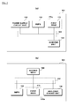
- FIG. 1 is a schematic block diagram illustrating an inverter assembly without galvanic isolation according to an exemplary embodiment of the present disclosure.
- an inverter assembly (100) without galvanic isolation may include a power supply circuit unit (110), an inverter unit (120), an analogue circuit unit (130), a controller (140), an SMPS (Switched-Mode Power Supply)(150), a first bead (170) and a second bead (180), where the power supply circuit unit (110), the n inverter unit (120), the analogue circuit unit (130), the controller (140), the SMPS (150), the first bead (170) and the second bead (180) may be mounted on a PCB (Printed Circuit Board, 101).
- PCB Print Circuit Board
- the power supply circuit unit (110) may include a rectifying circuit and a smoothing circuit, where the rectifying circuit may output an inputted AC (Alternating Current) power by rectifying the inputted AC power, and the smoothing circuit may output a DC (Direct Current) link voltage by smoothing an output voltage inputted from the rectifying circuit.
- the smoothing circuit may include a capacitor.
- the inverter unit (120) output a DC link voltage inputted from the power supply circuit unit (110) by converting the inputted DC link voltage to an AC voltage.
- the analogue circuit unit (130) may include a detection circuit configured to measure an output current of the inverter unit (120) or a DC link voltage and a protection circuit.
- the controller (140) may control the output of the inverter unit (120) in response to the output current measured by the analogue circuit unit (130) or the DC link voltage.
- the SMPS (150), an auxiliary power supply unit configured to supply an auxiliary power to the inverter unit (120), the analogue circuit unit (130) and the controller (140), is mounted to supply a stable power to the inverter unit (120), the analogue circuit unit (130) and the controller (140).
- the PCB (101) may be formed with the power supply circuit unit (110), the inverter unit (120) and a first ground circuit pattern (161) configured to supply a ground power to the SMPS (150).
- the PCB (101) may be formed with the analogue circuit unit (130) and a second ground circuit pattern (162) configured to supply a ground power to the SMPS (150).
- the PCB (101) may be formed with a third ground circuit pattern (163) configured to supply a ground power to the controller (140).
- the PCB (101) may be formed with a first bead (170) between the first ground circuit pattern (161) and the second ground circuit pattern (162).
- the first bead (170) may be formed for impedance isolation between the first ground circuit pattern (161) and the second ground circuit pattern (162).
- the first bead (170) may reduce or interrupt noise inflow through the impedance isolation between the first ground circuit pattern (161) and the second ground circuit pattern (162).
- the PCB (101) may be formed with a second bead (180) between the second ground circuit pattern (162) and the third ground circuit pattern (163).
- the second bead (180) may be formed for impedance isolation between the second ground circuit pattern (162) and the third ground circuit pattern (163).
- the second bead (180) may reduce or interrupt noise inflow through the impedance isolation between the second ground circuit pattern (162) and the third ground circuit pattern (163).
- the ground impedance of the controller (140), the analogue circuit unit (130) and the power supply circuit unit (110) can be isolated through the first and second beads (170, 180).
- the first and second beads (170, 180) may be configured to reduce or interrupt the harmonic noise.
- the first and second beads (170, 180) may be configured to reduce or interrupt the switching noise generated from the SMPS (150).
- the first and second beads (170, 180) may include an element configured to increase impedance at a particular harmonic area.
- the first and second beads (170, 180) may include a ferrite bead.
- the first and second beads (170, 180) may bring forth an effect of reducing a neighboring PK type noise in a CE measurement waveform between 150kHz and 200kHz, for example.
- the switching noise of the SMPS (150) may be effectively reduced or interrupted.
- FIG.2 is a schematic view illustrating a circuit pattern for impedance isolation between a power supply circuit unit and an analogue circuit unit in an inverter assembly without galvanic isolation according to an exemplary embodiment of the present disclosure.
- a first ground circuit pattern (161) of the power supply circuit unit (110) is illustrated in (a) and a second ground circuit pattern (162) of the analogue circuit unit (130) is illustrated in (b).
- the first and second ground circuit pattern (161, 162) may realize the impedance isolation through the first bead (170) mounted at a first bead pattern installation area (170a).
- the first bead (170) includes an element to increase impedance at a harmonic area, whereby the impedance isolation between the first and second ground circuit pattern (161, 162) can be effectively realized.
- the harmonic noise introduced to the second ground circuit pattern (162) from the first ground circuit pattern (161) can be effectively reduced or interrupted.
- FIG.3 is a schematic view illustrating a circuit pattern for impedance isolation between an analogue circuit unit and a controller in an inverter assembly without galvanic isolation according to an exemplary embodiment of the present disclosure, where (a) is illustrated with the second ground circuit pattern (162) of the analogue circuit unit (130), and (b) is illustrated with the third ground circuit pattern (163) of the controller (140).
- the second ground circuit pattern (162) and the third ground circuit pattern (163) may realize the impedance isolation through the second bead (180) mounted at a second bead pattern installation area (180a).
- the second bead (180) includes an element to increase an impedance at a harmonic area, whereby the impedance isolation between the second and third ground circuit pattern (162, 163) can be effectively realized.
- the harmonic noise introduced to the third ground circuit pattern (163) from the second ground circuit pattern (162) can be effectively reduced or interrupted.
- the exemplary embodiments of the present disclosure have an industrial applicability in that, although ground of a control circuit and a power supply circuit is not electrically isolated, an element configured to increase impedance in a particular harmonic area is inserted to impedance-isolate a control circuit ground circuit pattern from a ground circuit pattern of a power supply circuit on a harmonic area, whereby an effect of reinforcing harmonic noise resistance (immunity) in a harmonic area can be accomplished.
Landscapes
- Engineering & Computer Science (AREA)
- Microelectronics & Electronic Packaging (AREA)
- Power Engineering (AREA)
- Physics & Mathematics (AREA)
- Electromagnetism (AREA)
- Inverter Devices (AREA)
- Shielding Devices Or Components To Electric Or Magnetic Fields (AREA)
- Dc-Dc Converters (AREA)
Description
- The teachings in accordance with exemplary and non-limiting embodiments of the present disclosure relate generally to an inverter assembly without galvanic isolation, and particularly, to an inverter assembly without galvanic isolation configured to have a ground structure for noise-resistant reinforced characteristic in a small inverter where ground between an analog circuit and a power supply circuit is not electrically isolated.
- An inverter is a device configured to control a motor speed and a motor torque. Although there are several methods for motor speed control, representative methods include a primary voltage control method and a frequency modulation method. An inverter may be used for efficiency control and power factor control, and may be applied to and used for spare power source, non-interrupting electric source and linear transmission.
- The purpose of inverter is to perform a process control, factory automation and energy saving. For example, an inverter in a blower may adjust speed of the blower in response to types of product and output of the product. The adjustment of wind amount by a blower can adjust a temperature inside the blower to an optimum temperature, and promote improvement of product quality as well, whereby a great energy saving effect can be brought. Currently, researches on technologies for efficiently controlling an inverter are being briskly waged, in case an instantaneous interruption occurs.
- Conventionally, a design must be made in a manner such that an inverter is mounted with a noise prevention part on a power input unit in order to operate without erroneous operation caused by harmonic noise introduced from the power input unit or internal switching noise, or the ground of a control circuit, an analogue circuit and power supply circuit is electrically isolated to interrupt noise introduced from the power supply circuit to the control circuit or the analogue circuit.
- However, it is difficult to mount a noise prevention part to a power input unit, or to electrically isolate the ground of a control circuit, an analogue circuit and power supply circuit due to limit in product size, in case of a small-sized inverter product. An inverter that is not electrically isolated in the ground of power supply circuit has a structure susceptive to harmonic noise. A small-sized inverter cannot alleviate the harmonic noise introduced into an input unit due to difficulty in mounting a varistor on a 3-phase power input unit due to problem of product size.
- Although resistance to harmonic noise may be increased by designing a noise reduction filter on an inverter protection circuit, a sensing circuit and a connection unit of a control circuit, there is a limit due to generation of loss or delay of control information.
- Accordingly, the present disclosure is provided to solve the aforementioned problems/disadvantages, and therefore, it is an object of the present disclosure to provide an inverter assembly without galvanic isolation, and particularly, to an inverter assembly without galvanic isolation configured to have a ground structure for noise-resistant reinforced characteristic in a small inverter where ground between an analog circuit and a power supply circuit is not electrically isolated.
- It should be emphasized, however, that the present disclosure is not limited to a particular disclosure, as explained above. It should be understood that other technical subjects not mentioned herein may be appreciated by those skilled in the art.
- In order to accomplish the above object, in one general aspect of the present disclosure, there is provided an inverter assembly without galvanic isolation, the inverter comprising:
- a PCB (Printed Circuit Board) mounted with a power supply circuit unit, an inverter unit, an analogue circuit unit and a controller;
- a first ground circuit pattern mounted on the PCB and configured to supply a ground power to the power supply circuit unit and the inverter unit;
- a second ground circuit pattern mounted on the PCB and configured to supply the ground power to the analogue circuit unit;
- a third ground circuit pattern mounted on the PCB and configured to supply the ground power to the controller;
- a first bead mounted on the PCB between the first ground circuit pattern and the second ground circuit pattern to isolate an impedance between the first ground circuit pattern and the second ground circuit pattern;
- a second bead mounted on the PCB between the second ground circuit pattern and the third ground circuit pattern to isolate an impedance between the second ground circuit pattern and the third ground circuit pattern; and
- an auxiliary power supply unit mounted between the first ground circuit pattern and the second ground circuit pattern to supply an auxiliary power to the inverter unit.
- Preferably, but not necessarily, the first and second beads may be configured to reduce or interrupt a switching noise generated from the auxiliary power supply unit.
- Preferably, but not necessarily, the first and second beads may be configured to reduce or interrupt harmonic noise.
- Preferably, but not necessarily, an inverter assembly without galvanic isolation may further include an auxiliary power supply unit mounted between the first ground circuit pattern and the second ground circuit unit to supply an auxiliary power to the inverter unit, and the first and second beads may be configured to reduce or interrupt a switching noise generated from the auxiliary power supply unit.
- Preferably, but not necessarily, the first and second beads may include an element configured to increase impedance at a particular harmonic area.
- Preferably, but not necessarily, the first and second beads may include ferrite beads.
- Exemplary embodiments of inverter assembly without galvanic isolation have an advantageous effect in that, although ground of a control circuit and a power supply circuit is not electrically isolated, an element configured to increase impedance in a particular harmonic area is inserted to impedance-isolate a control circuit ground circuit pattern from a ground circuit pattern of a power supply circuit on a harmonic area, whereby an effect of reinforcing harmonic noise resistance (immunity) in a harmonic area can be accomplished.
-
-
FIG. 1 is a schematic block diagram illustrating an inverter assembly without galvanic isolation according to an exemplary embodiment of the present disclosure. -
FIG.2 is a schematic view illustrating a circuit pattern for impedance isolation between a power supply circuit unit and an analogue circuit unit in an inverter assembly without galvanic isolation according to an exemplary embodiment of the present disclosure. -
FIG.3 is a schematic view illustrating a circuit pattern for impedance isolation between an analogue circuit unit and a controller in an inverter assembly without galvanic isolation according to an exemplary embodiment of the present disclosure. - Various exemplary embodiments will be described more fully hereinafter with reference to the accompanying drawings, in which some exemplary embodiments are shown. The present inventive concept may, however, be embodied in many different forms and should not be construed as limited to the example embodiments set forth herein. Rather, the described aspect is intended to embrace all such alterations, modifications, and variations that fall within the scope and novel idea of the present disclosure.
- Accordingly, the meaning of specific terms or words used in the specification and claims should not be limited to the literal or commonly employed sense, but should be construed or may be different in accordance with the intention of a user or an operator and customary usages. Therefore, the definition of the specific terms or words should be based on the contents across the specification.
- That is, definitions of the terms "include" and "comprise," as well as derivatives thereof, may mean inclusion without limitation.
-
FIG. 1 is a schematic block diagram illustrating an inverter assembly without galvanic isolation according to an exemplary embodiment of the present disclosure. - Referring to
FIG. 1 , an inverter assembly (100) without galvanic isolation according to an exemplary embodiment of the present disclosure may include a power supply circuit unit (110), an inverter unit (120), an analogue circuit unit (130), a controller (140), an SMPS (Switched-Mode Power Supply)(150), a first bead (170) and a second bead (180), where the power supply circuit unit (110), the n inverter unit (120), the analogue circuit unit (130), the controller (140), the SMPS (150), the first bead (170) and the second bead (180) may be mounted on a PCB (Printed Circuit Board, 101). - The power supply circuit unit (110) may include a rectifying circuit and a smoothing circuit, where the rectifying circuit may output an inputted AC (Alternating Current) power by rectifying the inputted AC power, and the smoothing circuit may output a DC (Direct Current) link voltage by smoothing an output voltage inputted from the rectifying circuit. The smoothing circuit may include a capacitor.
- The inverter unit (120) output a DC link voltage inputted from the power supply circuit unit (110) by converting the inputted DC link voltage to an AC voltage. The analogue circuit unit (130) may include a detection circuit configured to measure an output current of the inverter unit (120) or a DC link voltage and a protection circuit. The controller (140) may control the output of the inverter unit (120) in response to the output current measured by the analogue circuit unit (130) or the DC link voltage. The SMPS (150), an auxiliary power supply unit configured to supply an auxiliary power to the inverter unit (120), the analogue circuit unit (130) and the controller (140), is mounted to supply a stable power to the inverter unit (120), the analogue circuit unit (130) and the controller (140).
- When R, S, T 3-phase AC power or a single-phase AC power is supplied to the power supply circuit unit (110), the inputted AC power is charged in a DC link capacitor which is a smoothing circuit through a diode bridge which is a rectifying circuit. When the DC link voltage increases, the SMPS (150) is activated whereby an operation power is supplied to the controller (140) and the analogue circuit unit (130). The DC supplied to the power supply circuit unit (110) is switched by the inverter unit (120) to be outputted to a 3-phase AC power (U, V, W).
- Meantime, the PCB (101) may be formed with the power supply circuit unit (110), the inverter unit (120) and a first ground circuit pattern (161) configured to supply a ground power to the SMPS (150). The PCB (101) may be formed with the analogue circuit unit (130) and a second ground circuit pattern (162) configured to supply a ground power to the SMPS (150). The PCB (101) may be formed with a third ground circuit pattern (163) configured to supply a ground power to the controller (140).
- The PCB (101) may be formed with a first bead (170) between the first ground circuit pattern (161) and the second ground circuit pattern (162). The first bead (170) may be formed for impedance isolation between the first ground circuit pattern (161) and the second ground circuit pattern (162). The first bead (170) may reduce or interrupt noise inflow through the impedance isolation between the first ground circuit pattern (161) and the second ground circuit pattern (162).
- The PCB (101) may be formed with a second bead (180) between the second ground circuit pattern (162) and the third ground circuit pattern (163). The second bead (180) may be formed for impedance isolation between the second ground circuit pattern (162) and the third ground circuit pattern (163). The second bead (180) may reduce or interrupt noise inflow through the impedance isolation between the second ground circuit pattern (162) and the third ground circuit pattern (163).
- As noted from the foregoing, the ground impedance of the controller (140), the analogue circuit unit (130) and the power supply circuit unit (110) can be isolated through the first and second beads (170, 180). The first and second beads (170, 180) may be configured to reduce or interrupt the harmonic noise. The first and second beads (170, 180) may be configured to reduce or interrupt the switching noise generated from the SMPS (150).
- The first and second beads (170, 180) may include an element configured to increase impedance at a particular harmonic area. For example, the first and second beads (170, 180) may include a ferrite bead. The first and second beads (170, 180) may bring forth an effect of reducing a neighboring PK type noise in a CE measurement waveform between 150kHz and 200kHz, for example.
- When an SMPS (150) whose switching frequency is 170kHz is used, the switching noise of the SMPS (150) may be effectively reduced or interrupted.
-
FIG.2 is a schematic view illustrating a circuit pattern for impedance isolation between a power supply circuit unit and an analogue circuit unit in an inverter assembly without galvanic isolation according to an exemplary embodiment of the present disclosure. - Referring to
FIG. 2 , a first ground circuit pattern (161) of the power supply circuit unit (110) is illustrated in (a) and a second ground circuit pattern (162) of the analogue circuit unit (130) is illustrated in (b). The first and second ground circuit pattern (161, 162) may realize the impedance isolation through the first bead (170) mounted at a first bead pattern installation area (170a). The first bead (170) includes an element to increase impedance at a harmonic area, whereby the impedance isolation between the first and second ground circuit pattern (161, 162) can be effectively realized. As a result, the harmonic noise introduced to the second ground circuit pattern (162) from the first ground circuit pattern (161) can be effectively reduced or interrupted. -
FIG.3 is a schematic view illustrating a circuit pattern for impedance isolation between an analogue circuit unit and a controller in an inverter assembly without galvanic isolation according to an exemplary embodiment of the present disclosure, where (a) is illustrated with the second ground circuit pattern (162) of the analogue circuit unit (130), and (b) is illustrated with the third ground circuit pattern (163) of the controller (140). - The second ground circuit pattern (162) and the third ground circuit pattern (163) may realize the impedance isolation through the second bead (180) mounted at a second bead pattern installation area (180a). The second bead (180) includes an element to increase an impedance at a harmonic area, whereby the impedance isolation between the second and third ground circuit pattern (162, 163) can be effectively realized. As a result, the harmonic noise introduced to the third ground circuit pattern (163) from the second ground circuit pattern (162) can be effectively reduced or interrupted.
- The previous illustrative description of the present disclosure is provided to enable any person skilled in the art to make or use the invention. Various modifications to the invention will be readily apparent to those skilled in the art, and the generic principles defined herein may be applied to other variations without departing from the spirit or scope of the invention. Thus, the invention is not intended to limit the examples described herein, but is to be accorded the widest scope consistent with the principles and novel features disclosed herein.
- The exemplary embodiments of the present disclosure have an industrial applicability in that, although ground of a control circuit and a power supply circuit is not electrically isolated, an element configured to increase impedance in a particular harmonic area is inserted to impedance-isolate a control circuit ground circuit pattern from a ground circuit pattern of a power supply circuit on a harmonic area, whereby an effect of reinforcing harmonic noise resistance (immunity) in a harmonic area can be accomplished.
Claims (4)
- An inverter assembly without galvanic isolation, the inverter characterized by:a PCB (101, Printed Circuit Board) mounted with a power supply circuit unit (110), an inverter unit (120), an analogue circuit unit (130) and a controller (140);a first ground circuit pattern (161) mounted on the PCB (101) and configured to supply a ground power to the power supply circuit unit (110) and the inverter unit (120);a second ground circuit pattern (162) mounted on the PCB (101) and configured to supply the ground power to the analogue circuit unit (130);a third ground circuit pattern (163) mounted on the PCB (101) and configured to supply the ground power to the controller (140);a first bead (170) mounted on the PCB (101) between the first ground circuit pattern (161) and the second ground circuit pattern (162) to isolate an impedance between the first ground circuit pattern (161) and the second ground circuit pattern (162);a second bead (180) mounted on the PCB (101) between the second ground circuit pattern (162) and the third ground circuit pattern (163) to isolate an impedance between the second ground circuit pattern (162) and the third ground circuit pattern (163); andan auxiliary power supply unit (150) mounted between the first ground circuit pattern (161) and the second ground circuit pattern (162) to supply an auxiliary power to the inverter unit (120), whereinthe first and second beads (170, 180) are configured to reduce or interrupt a switching noise generated from the auxiliary power supply unit (150).
- The inverter assembly of claim 1, characterized in that the first and second beads (170, 180) are configured to reduce or interrupt harmonic noise.
- The inverter assembly of claim 1 or 2, characterized in that the first and second beads (170, 180) include an element configured to increase impedance at a particular harmonic area.
- The inverter assembly of claim 3, characterized in that the first and second beads (170, 180) include ferrite beads.
Applications Claiming Priority (1)
| Application Number | Priority Date | Filing Date | Title |
|---|---|---|---|
| KR1020140093070A KR20160011867A (en) | 2014-07-23 | 2014-07-23 | Inverter assembly without galvanic isolation |
Publications (2)
| Publication Number | Publication Date |
|---|---|
| EP2978121A1 true EP2978121A1 (en) | 2016-01-27 |
| EP2978121B1 EP2978121B1 (en) | 2021-11-24 |
Family
ID=53682528
Family Applications (1)
| Application Number | Title | Priority Date | Filing Date |
|---|---|---|---|
| EP15176483.4A Active EP2978121B1 (en) | 2014-07-23 | 2015-07-13 | Inverter assembly without galvanic isolation |
Country Status (6)
| Country | Link |
|---|---|
| US (1) | US9577507B2 (en) |
| EP (1) | EP2978121B1 (en) |
| JP (1) | JP6042946B2 (en) |
| KR (1) | KR20160011867A (en) |
| CN (1) | CN105322762B (en) |
| ES (1) | ES2904279T3 (en) |
Families Citing this family (2)
| Publication number | Priority date | Publication date | Assignee | Title |
|---|---|---|---|---|
| EP3405531B1 (en) * | 2016-01-21 | 2023-10-04 | Swimc LLC | High reflectance coating |
| KR101821878B1 (en) * | 2016-02-24 | 2018-01-24 | 엘에스산전 주식회사 | Inverter |
Citations (3)
| Publication number | Priority date | Publication date | Assignee | Title |
|---|---|---|---|---|
| JP2000269613A (en) * | 1999-03-18 | 2000-09-29 | Matsushita Electric Ind Co Ltd | Unwanted radiation printed circuit board |
| US20050253830A1 (en) * | 2004-04-29 | 2005-11-17 | Dong-Hyup Jeon | Electron emission display (EED) with separated grounds |
| EP1912488A2 (en) * | 2006-10-13 | 2008-04-16 | Mitsubishi Heavy Industries, Ltd. | Control board and control apparatus |
Family Cites Families (10)
| Publication number | Priority date | Publication date | Assignee | Title |
|---|---|---|---|---|
| JP3581971B2 (en) * | 1996-05-22 | 2004-10-27 | 株式会社ボッシュオートモーティブシステム | EMI grounding structure for in-vehicle control unit |
| US6084779A (en) * | 1998-10-02 | 2000-07-04 | Sigrity, Inc. | Ground and power patches on printed circuit board signal planes in the areas of integrated circuit chips |
| US6714092B1 (en) * | 2000-11-02 | 2004-03-30 | Intel Corporation | Supply noise filter for clock generator |
| KR100460510B1 (en) | 2002-05-02 | 2004-12-08 | 엘지전자 주식회사 | Frequency conversion unit comprising multiple isolated grounds in mobile communication system |
| KR20040043060A (en) | 2002-11-15 | 2004-05-22 | 엘지전자 주식회사 | A circuit for controlling lamp of LCD monitor |
| JP4671333B2 (en) | 2005-03-18 | 2011-04-13 | 株式会社リコー | Multilayer printed circuit board and electronic equipment |
| JP5437558B2 (en) | 2006-11-16 | 2014-03-12 | 三菱電機株式会社 | Electromagnetic noise countermeasure structure for printed circuit boards |
| US8203232B2 (en) * | 2009-12-10 | 2012-06-19 | Lear Corporation | Embedded wireless communications for electronic control unit having multiple ground references |
| JP5448797B2 (en) * | 2009-12-25 | 2014-03-19 | 三菱重工業株式会社 | Control board, inverter device, and inverter-integrated electric compressor |
| US8970148B2 (en) * | 2012-07-31 | 2015-03-03 | Rockwell Automation Technologies, Inc. | Method and apparatus for reducing radiated emissions in switching power converters |
-
2014
- 2014-07-23 KR KR1020140093070A patent/KR20160011867A/en not_active Ceased
-
2015
- 2015-06-19 US US14/745,218 patent/US9577507B2/en active Active
- 2015-07-10 JP JP2015138491A patent/JP6042946B2/en not_active Expired - Fee Related
- 2015-07-13 ES ES15176483T patent/ES2904279T3/en active Active
- 2015-07-13 EP EP15176483.4A patent/EP2978121B1/en active Active
- 2015-07-23 CN CN201510438273.9A patent/CN105322762B/en active Active
Patent Citations (3)
| Publication number | Priority date | Publication date | Assignee | Title |
|---|---|---|---|---|
| JP2000269613A (en) * | 1999-03-18 | 2000-09-29 | Matsushita Electric Ind Co Ltd | Unwanted radiation printed circuit board |
| US20050253830A1 (en) * | 2004-04-29 | 2005-11-17 | Dong-Hyup Jeon | Electron emission display (EED) with separated grounds |
| EP1912488A2 (en) * | 2006-10-13 | 2008-04-16 | Mitsubishi Heavy Industries, Ltd. | Control board and control apparatus |
Non-Patent Citations (1)
| Title |
|---|
| ARMSTRONG M K: "PCB DESIGN TECHNIQUES FOR LOWEST-COST EMC COMPLIANCE: PART 1", ELECTRONICS AND COMMUNICATION ENGINEERING JOURNAL, INSTITUTION OF ELECTRICAL ENGINEERS, LONDON, GB, vol. 11, no. 4, 1 August 1999 (1999-08-01), pages 185 - 194, XP000930518, ISSN: 0954-0695, DOI: 10.1049/ECEJ:19990402 * |
Also Published As
| Publication number | Publication date |
|---|---|
| JP6042946B2 (en) | 2016-12-14 |
| ES2904279T3 (en) | 2022-04-04 |
| US9577507B2 (en) | 2017-02-21 |
| US20160028300A1 (en) | 2016-01-28 |
| CN105322762B (en) | 2018-04-03 |
| CN105322762A (en) | 2016-02-10 |
| JP2016025844A (en) | 2016-02-08 |
| KR20160011867A (en) | 2016-02-02 |
| EP2978121B1 (en) | 2021-11-24 |
Similar Documents
| Publication | Publication Date | Title |
|---|---|---|
| US9516708B2 (en) | Method for operating an LLC resonant converter for a light-emitting means, converter, and LED converter device | |
| TWI531141B (en) | Noise eliminating method and adapter | |
| US9647525B2 (en) | Power supply device with current limit based on output current and input voltage | |
| JP6479160B2 (en) | Converter device | |
| TWI523395B (en) | Control methods for clock frequency in a switched mode power supply and relevant power controllers | |
| US9577507B2 (en) | Inverter assembly without galvanic isolation | |
| US9300204B2 (en) | Switching power supply | |
| EP2874298B1 (en) | Pre-charging circuit for an inverter | |
| KR101326004B1 (en) | Illuminator having a protection circuit | |
| CN103229407B (en) | DC power supply unit | |
| KR101120429B1 (en) | Charging circuit of battery for forklift truck | |
| KR20120019927A (en) | Arc detecting circuit having transient arc detecting function and power supply apparatus for generation of atmospheric plasma by using the same | |
| KR102372846B1 (en) | Control circuit of power factor correction converter operating in critical conduction mode and power factor correction converter comprising thtereof | |
| KR101667265B1 (en) | Protective circuit for high frequency heating device and high frequency heating device having same | |
| CN110099469B (en) | Electromagnetic induction heating device and protection control circuit thereof | |
| CN103124145A (en) | Three-phase rectifying device | |
| KR100655245B1 (en) | High efficiency plasma inverter | |
| JP5892842B2 (en) | Induction heating cooker | |
| KR200422688Y1 (en) | High efficiency plasma inverter | |
| JP2005209563A (en) | Electromagnetic induction heating cooker | |
| JP6293014B2 (en) | Switching power supply | |
| EP2892143A1 (en) | AC power supply | |
| KR20130083601A (en) | Switched mode power supply having a function of overvoltage protection | |
| JP2009219316A (en) | Power supply circuit | |
| CN105656325A (en) | Power supply device with alternating current power supply detection circuit |
Legal Events
| Date | Code | Title | Description |
|---|---|---|---|
| PUAI | Public reference made under article 153(3) epc to a published international application that has entered the european phase |
Free format text: ORIGINAL CODE: 0009012 |
|
| AK | Designated contracting states |
Kind code of ref document: A1 Designated state(s): AL AT BE BG CH CY CZ DE DK EE ES FI FR GB GR HR HU IE IS IT LI LT LU LV MC MK MT NL NO PL PT RO RS SE SI SK SM TR |
|
| AX | Request for extension of the european patent |
Extension state: BA ME |
|
| 17P | Request for examination filed |
Effective date: 20160726 |
|
| RBV | Designated contracting states (corrected) |
Designated state(s): AL AT BE BG CH CY CZ DE DK EE ES FI FR GB GR HR HU IE IS IT LI LT LU LV MC MK MT NL NO PL PT RO RS SE SI SK SM TR |
|
| R17P | Request for examination filed (corrected) |
Effective date: 20160726 |
|
| STAA | Information on the status of an ep patent application or granted ep patent |
Free format text: STATUS: EXAMINATION IS IN PROGRESS |
|
| 17Q | First examination report despatched |
Effective date: 20180918 |
|
| REG | Reference to a national code |
Ref country code: DE Ref legal event code: R079 Ref document number: 602015075191 Country of ref document: DE Free format text: PREVIOUS MAIN CLASS: H02M0007480000 Ipc: H05K0001020000 |
|
| GRAP | Despatch of communication of intention to grant a patent |
Free format text: ORIGINAL CODE: EPIDOSNIGR1 |
|
| STAA | Information on the status of an ep patent application or granted ep patent |
Free format text: STATUS: GRANT OF PATENT IS INTENDED |
|
| RIC1 | Information provided on ipc code assigned before grant |
Ipc: H05K 1/02 20060101AFI20210607BHEP Ipc: H02M 1/12 20060101ALI20210607BHEP Ipc: H02M 7/48 20070101ALI20210607BHEP Ipc: H02M 7/00 20060101ALI20210607BHEP |
|
| INTG | Intention to grant announced |
Effective date: 20210701 |
|
| GRAS | Grant fee paid |
Free format text: ORIGINAL CODE: EPIDOSNIGR3 |
|
| GRAA | (expected) grant |
Free format text: ORIGINAL CODE: 0009210 |
|
| STAA | Information on the status of an ep patent application or granted ep patent |
Free format text: STATUS: THE PATENT HAS BEEN GRANTED |
|
| AK | Designated contracting states |
Kind code of ref document: B1 Designated state(s): AL AT BE BG CH CY CZ DE DK EE ES FI FR GB GR HR HU IE IS IT LI LT LU LV MC MK MT NL NO PL PT RO RS SE SI SK SM TR |
|
| REG | Reference to a national code |
Ref country code: GB Ref legal event code: FG4D |
|
| REG | Reference to a national code |
Ref country code: AT Ref legal event code: REF Ref document number: 1450874 Country of ref document: AT Kind code of ref document: T Effective date: 20211215 |
|
| REG | Reference to a national code |
Ref country code: DE Ref legal event code: R096 Ref document number: 602015075191 Country of ref document: DE |
|
| REG | Reference to a national code |
Ref country code: IE Ref legal event code: FG4D |
|
| REG | Reference to a national code |
Ref country code: LT Ref legal event code: MG9D |
|
| REG | Reference to a national code |
Ref country code: NL Ref legal event code: MP Effective date: 20211124 |
|
| REG | Reference to a national code |
Ref country code: ES Ref legal event code: FG2A Ref document number: 2904279 Country of ref document: ES Kind code of ref document: T3 Effective date: 20220404 |
|
| REG | Reference to a national code |
Ref country code: AT Ref legal event code: MK05 Ref document number: 1450874 Country of ref document: AT Kind code of ref document: T Effective date: 20211124 |
|
| PG25 | Lapsed in a contracting state [announced via postgrant information from national office to epo] |
Ref country code: RS Free format text: LAPSE BECAUSE OF FAILURE TO SUBMIT A TRANSLATION OF THE DESCRIPTION OR TO PAY THE FEE WITHIN THE PRESCRIBED TIME-LIMIT Effective date: 20211124 Ref country code: LT Free format text: LAPSE BECAUSE OF FAILURE TO SUBMIT A TRANSLATION OF THE DESCRIPTION OR TO PAY THE FEE WITHIN THE PRESCRIBED TIME-LIMIT Effective date: 20211124 Ref country code: FI Free format text: LAPSE BECAUSE OF FAILURE TO SUBMIT A TRANSLATION OF THE DESCRIPTION OR TO PAY THE FEE WITHIN THE PRESCRIBED TIME-LIMIT Effective date: 20211124 Ref country code: BG Free format text: LAPSE BECAUSE OF FAILURE TO SUBMIT A TRANSLATION OF THE DESCRIPTION OR TO PAY THE FEE WITHIN THE PRESCRIBED TIME-LIMIT Effective date: 20220224 Ref country code: AT Free format text: LAPSE BECAUSE OF FAILURE TO SUBMIT A TRANSLATION OF THE DESCRIPTION OR TO PAY THE FEE WITHIN THE PRESCRIBED TIME-LIMIT Effective date: 20211124 |
|
| PG25 | Lapsed in a contracting state [announced via postgrant information from national office to epo] |
Ref country code: IS Free format text: LAPSE BECAUSE OF FAILURE TO SUBMIT A TRANSLATION OF THE DESCRIPTION OR TO PAY THE FEE WITHIN THE PRESCRIBED TIME-LIMIT Effective date: 20220324 Ref country code: SE Free format text: LAPSE BECAUSE OF FAILURE TO SUBMIT A TRANSLATION OF THE DESCRIPTION OR TO PAY THE FEE WITHIN THE PRESCRIBED TIME-LIMIT Effective date: 20211124 Ref country code: PT Free format text: LAPSE BECAUSE OF FAILURE TO SUBMIT A TRANSLATION OF THE DESCRIPTION OR TO PAY THE FEE WITHIN THE PRESCRIBED TIME-LIMIT Effective date: 20220324 Ref country code: PL Free format text: LAPSE BECAUSE OF FAILURE TO SUBMIT A TRANSLATION OF THE DESCRIPTION OR TO PAY THE FEE WITHIN THE PRESCRIBED TIME-LIMIT Effective date: 20211124 Ref country code: NO Free format text: LAPSE BECAUSE OF FAILURE TO SUBMIT A TRANSLATION OF THE DESCRIPTION OR TO PAY THE FEE WITHIN THE PRESCRIBED TIME-LIMIT Effective date: 20220224 Ref country code: NL Free format text: LAPSE BECAUSE OF FAILURE TO SUBMIT A TRANSLATION OF THE DESCRIPTION OR TO PAY THE FEE WITHIN THE PRESCRIBED TIME-LIMIT Effective date: 20211124 Ref country code: LV Free format text: LAPSE BECAUSE OF FAILURE TO SUBMIT A TRANSLATION OF THE DESCRIPTION OR TO PAY THE FEE WITHIN THE PRESCRIBED TIME-LIMIT Effective date: 20211124 Ref country code: HR Free format text: LAPSE BECAUSE OF FAILURE TO SUBMIT A TRANSLATION OF THE DESCRIPTION OR TO PAY THE FEE WITHIN THE PRESCRIBED TIME-LIMIT Effective date: 20211124 Ref country code: GR Free format text: LAPSE BECAUSE OF FAILURE TO SUBMIT A TRANSLATION OF THE DESCRIPTION OR TO PAY THE FEE WITHIN THE PRESCRIBED TIME-LIMIT Effective date: 20220225 |
|
| PG25 | Lapsed in a contracting state [announced via postgrant information from national office to epo] |
Ref country code: SM Free format text: LAPSE BECAUSE OF FAILURE TO SUBMIT A TRANSLATION OF THE DESCRIPTION OR TO PAY THE FEE WITHIN THE PRESCRIBED TIME-LIMIT Effective date: 20211124 Ref country code: SK Free format text: LAPSE BECAUSE OF FAILURE TO SUBMIT A TRANSLATION OF THE DESCRIPTION OR TO PAY THE FEE WITHIN THE PRESCRIBED TIME-LIMIT Effective date: 20211124 Ref country code: RO Free format text: LAPSE BECAUSE OF FAILURE TO SUBMIT A TRANSLATION OF THE DESCRIPTION OR TO PAY THE FEE WITHIN THE PRESCRIBED TIME-LIMIT Effective date: 20211124 Ref country code: EE Free format text: LAPSE BECAUSE OF FAILURE TO SUBMIT A TRANSLATION OF THE DESCRIPTION OR TO PAY THE FEE WITHIN THE PRESCRIBED TIME-LIMIT Effective date: 20211124 Ref country code: DK Free format text: LAPSE BECAUSE OF FAILURE TO SUBMIT A TRANSLATION OF THE DESCRIPTION OR TO PAY THE FEE WITHIN THE PRESCRIBED TIME-LIMIT Effective date: 20211124 Ref country code: CZ Free format text: LAPSE BECAUSE OF FAILURE TO SUBMIT A TRANSLATION OF THE DESCRIPTION OR TO PAY THE FEE WITHIN THE PRESCRIBED TIME-LIMIT Effective date: 20211124 |
|
| PGFP | Annual fee paid to national office [announced via postgrant information from national office to epo] |
Ref country code: GB Payment date: 20220607 Year of fee payment: 8 |
|
| REG | Reference to a national code |
Ref country code: DE Ref legal event code: R097 Ref document number: 602015075191 Country of ref document: DE |
|
| PLBE | No opposition filed within time limit |
Free format text: ORIGINAL CODE: 0009261 |
|
| STAA | Information on the status of an ep patent application or granted ep patent |
Free format text: STATUS: NO OPPOSITION FILED WITHIN TIME LIMIT |
|
| PG25 | Lapsed in a contracting state [announced via postgrant information from national office to epo] |
Ref country code: AL Free format text: LAPSE BECAUSE OF FAILURE TO SUBMIT A TRANSLATION OF THE DESCRIPTION OR TO PAY THE FEE WITHIN THE PRESCRIBED TIME-LIMIT Effective date: 20211124 |
|
| PGFP | Annual fee paid to national office [announced via postgrant information from national office to epo] |
Ref country code: ES Payment date: 20220811 Year of fee payment: 8 |
|
| 26N | No opposition filed |
Effective date: 20220825 |
|
| PG25 | Lapsed in a contracting state [announced via postgrant information from national office to epo] |
Ref country code: SI Free format text: LAPSE BECAUSE OF FAILURE TO SUBMIT A TRANSLATION OF THE DESCRIPTION OR TO PAY THE FEE WITHIN THE PRESCRIBED TIME-LIMIT Effective date: 20211124 |
|
| PG25 | Lapsed in a contracting state [announced via postgrant information from national office to epo] |
Ref country code: MC Free format text: LAPSE BECAUSE OF FAILURE TO SUBMIT A TRANSLATION OF THE DESCRIPTION OR TO PAY THE FEE WITHIN THE PRESCRIBED TIME-LIMIT Effective date: 20211124 |
|
| REG | Reference to a national code |
Ref country code: CH Ref legal event code: PL |
|
| REG | Reference to a national code |
Ref country code: BE Ref legal event code: MM Effective date: 20220731 |
|
| PG25 | Lapsed in a contracting state [announced via postgrant information from national office to epo] |
Ref country code: LU Free format text: LAPSE BECAUSE OF NON-PAYMENT OF DUE FEES Effective date: 20220713 Ref country code: LI Free format text: LAPSE BECAUSE OF NON-PAYMENT OF DUE FEES Effective date: 20220731 Ref country code: FR Free format text: LAPSE BECAUSE OF NON-PAYMENT OF DUE FEES Effective date: 20220731 Ref country code: CH Free format text: LAPSE BECAUSE OF NON-PAYMENT OF DUE FEES Effective date: 20220731 |
|
| PG25 | Lapsed in a contracting state [announced via postgrant information from national office to epo] |
Ref country code: BE Free format text: LAPSE BECAUSE OF NON-PAYMENT OF DUE FEES Effective date: 20220731 |
|
| PG25 | Lapsed in a contracting state [announced via postgrant information from national office to epo] |
Ref country code: IE Free format text: LAPSE BECAUSE OF NON-PAYMENT OF DUE FEES Effective date: 20220713 |
|
| P01 | Opt-out of the competence of the unified patent court (upc) registered |
Effective date: 20230625 |
|
| GBPC | Gb: european patent ceased through non-payment of renewal fee |
Effective date: 20230713 |
|
| PG25 | Lapsed in a contracting state [announced via postgrant information from national office to epo] |
Ref country code: HU Free format text: LAPSE BECAUSE OF FAILURE TO SUBMIT A TRANSLATION OF THE DESCRIPTION OR TO PAY THE FEE WITHIN THE PRESCRIBED TIME-LIMIT; INVALID AB INITIO Effective date: 20150713 |
|
| PG25 | Lapsed in a contracting state [announced via postgrant information from national office to epo] |
Ref country code: MK Free format text: LAPSE BECAUSE OF FAILURE TO SUBMIT A TRANSLATION OF THE DESCRIPTION OR TO PAY THE FEE WITHIN THE PRESCRIBED TIME-LIMIT Effective date: 20211124 Ref country code: CY Free format text: LAPSE BECAUSE OF FAILURE TO SUBMIT A TRANSLATION OF THE DESCRIPTION OR TO PAY THE FEE WITHIN THE PRESCRIBED TIME-LIMIT Effective date: 20211124 Ref country code: GB Free format text: LAPSE BECAUSE OF NON-PAYMENT OF DUE FEES Effective date: 20230713 |
|
| PG25 | Lapsed in a contracting state [announced via postgrant information from national office to epo] |
Ref country code: TR Free format text: LAPSE BECAUSE OF FAILURE TO SUBMIT A TRANSLATION OF THE DESCRIPTION OR TO PAY THE FEE WITHIN THE PRESCRIBED TIME-LIMIT Effective date: 20211124 |
|
| REG | Reference to a national code |
Ref country code: ES Ref legal event code: FD2A Effective date: 20240828 |
|
| PG25 | Lapsed in a contracting state [announced via postgrant information from national office to epo] |
Ref country code: MT Free format text: LAPSE BECAUSE OF FAILURE TO SUBMIT A TRANSLATION OF THE DESCRIPTION OR TO PAY THE FEE WITHIN THE PRESCRIBED TIME-LIMIT Effective date: 20211124 |
|
| PG25 | Lapsed in a contracting state [announced via postgrant information from national office to epo] |
Ref country code: ES Free format text: LAPSE BECAUSE OF NON-PAYMENT OF DUE FEES Effective date: 20230714 |
|
| PG25 | Lapsed in a contracting state [announced via postgrant information from national office to epo] |
Ref country code: ES Free format text: LAPSE BECAUSE OF NON-PAYMENT OF DUE FEES Effective date: 20230714 |
|
| PGFP | Annual fee paid to national office [announced via postgrant information from national office to epo] |
Ref country code: DE Payment date: 20250609 Year of fee payment: 11 |
|
| PGFP | Annual fee paid to national office [announced via postgrant information from national office to epo] |
Ref country code: IT Payment date: 20250610 Year of fee payment: 11 |