EP2974008B1 - Buffer amplifier circuit - Google Patents
Buffer amplifier circuit Download PDFInfo
- Publication number
- EP2974008B1 EP2974008B1 EP14768045.8A EP14768045A EP2974008B1 EP 2974008 B1 EP2974008 B1 EP 2974008B1 EP 14768045 A EP14768045 A EP 14768045A EP 2974008 B1 EP2974008 B1 EP 2974008B1
- Authority
- EP
- European Patent Office
- Prior art keywords
- voltage
- circuit
- input
- amplifier
- switches
- Prior art date
- Legal status (The legal status is an assumption and is not a legal conclusion. Google has not performed a legal analysis and makes no representation as to the accuracy of the status listed.)
- Active
Links
Images


Classifications
-
- H—ELECTRICITY
- H03—ELECTRONIC CIRCUITRY
- H03F—AMPLIFIERS
- H03F3/00—Amplifiers with only discharge tubes or only semiconductor devices as amplifying elements
- H03F3/04—Amplifiers with only discharge tubes or only semiconductor devices as amplifying elements with semiconductor devices only
- H03F3/16—Amplifiers with only discharge tubes or only semiconductor devices as amplifying elements with semiconductor devices only with field-effect devices
-
- H—ELECTRICITY
- H03—ELECTRONIC CIRCUITRY
- H03F—AMPLIFIERS
- H03F3/00—Amplifiers with only discharge tubes or only semiconductor devices as amplifying elements
- H03F3/62—Two-way amplifiers
-
- G—PHYSICS
- G11—INFORMATION STORAGE
- G11C—STATIC STORES
- G11C27/00—Electric analogue stores, e.g. for storing instantaneous values
- G11C27/02—Sample-and-hold arrangements
- G11C27/024—Sample-and-hold arrangements using a capacitive memory element
-
- H—ELECTRICITY
- H03—ELECTRONIC CIRCUITRY
- H03F—AMPLIFIERS
- H03F3/00—Amplifiers with only discharge tubes or only semiconductor devices as amplifying elements
- H03F3/005—Amplifiers with only discharge tubes or only semiconductor devices as amplifying elements using switched capacitors, e.g. dynamic amplifiers; using switched capacitors as resistors in differential amplifiers
-
- H—ELECTRICITY
- H03—ELECTRONIC CIRCUITRY
- H03F—AMPLIFIERS
- H03F3/00—Amplifiers with only discharge tubes or only semiconductor devices as amplifying elements
- H03F3/70—Charge amplifiers
-
- H—ELECTRICITY
- H03—ELECTRONIC CIRCUITRY
- H03H—IMPEDANCE NETWORKS, e.g. RESONANT CIRCUITS; RESONATORS
- H03H19/00—Networks using time-varying elements, e.g. N-path filters
- H03H19/004—Switched capacitor networks
-
- H—ELECTRICITY
- H03—ELECTRONIC CIRCUITRY
- H03F—AMPLIFIERS
- H03F2200/00—Indexing scheme relating to amplifiers
- H03F2200/156—One or more switches are realised in the feedback circuit of the amplifier stage
-
- H—ELECTRICITY
- H03—ELECTRONIC CIRCUITRY
- H03F—AMPLIFIERS
- H03F2200/00—Indexing scheme relating to amplifiers
- H03F2200/159—Indexing scheme relating to amplifiers the feedback circuit being closed during a switching time
-
- H—ELECTRICITY
- H03—ELECTRONIC CIRCUITRY
- H03F—AMPLIFIERS
- H03F2200/00—Indexing scheme relating to amplifiers
- H03F2200/357—Indexing scheme relating to amplifiers the amplifier comprising MOS which are biased in the weak inversion region
-
- H—ELECTRICITY
- H03—ELECTRONIC CIRCUITRY
- H03F—AMPLIFIERS
- H03F2200/00—Indexing scheme relating to amplifiers
- H03F2200/42—Indexing scheme relating to amplifiers the input to the amplifier being made by capacitive coupling means
-
- H—ELECTRICITY
- H03—ELECTRONIC CIRCUITRY
- H03M—CODING; DECODING; CODE CONVERSION IN GENERAL
- H03M1/00—Analogue/digital conversion; Digital/analogue conversion
- H03M1/12—Analogue/digital converters
- H03M1/124—Sampling or signal conditioning arrangements specially adapted for A/D converters
- H03M1/1245—Details of sampling arrangements or methods
-
- H—ELECTRICITY
- H03—ELECTRONIC CIRCUITRY
- H03M—CODING; DECODING; CODE CONVERSION IN GENERAL
- H03M1/00—Analogue/digital conversion; Digital/analogue conversion
- H03M1/12—Analogue/digital converters
- H03M1/34—Analogue value compared with reference values
- H03M1/38—Analogue value compared with reference values sequentially only, e.g. successive approximation type
- H03M1/46—Analogue value compared with reference values sequentially only, e.g. successive approximation type with digital/analogue converter for supplying reference values to converter
- H03M1/466—Analogue value compared with reference values sequentially only, e.g. successive approximation type with digital/analogue converter for supplying reference values to converter using switched capacitors
- H03M1/468—Analogue value compared with reference values sequentially only, e.g. successive approximation type with digital/analogue converter for supplying reference values to converter using switched capacitors in which the input S/H circuit is merged with the feedback DAC array
Definitions
- This application is directed to microelectronic circuits and circuit design and operation. More particularly, this application is directed to microelectronic amplifier circuits for use in semiconductor devices, integrated circuits and other electronic devices.
- LNA low-noise amplifier
- a low-noise amplifier (LNA) in the receiver amplifies the tiny signal picked up by an antenna.
- the amplified signal is then filtered, demodulated and further amplified again.
- the signal is often converted to a digital signal by an analog-to-digital converter.
- the analog-to-digital converter also typically amplifies the signal in the conversion process.
- the power amplifier amplifies the radio frequency signal before the signal is transmitted through the antenna.
- sensors such as image sensors, microphones, and micro-electromechanical sensors, the signal produced by the sensors is very small, and thus must be amplified before further signal processing.
- CMOS complementary metal-oxide-semiconductor
- MOS complementary metal-oxide-semiconductor
- MOS complementary metal-oxide-semiconductor
- the first two types typically provide a substantial amount of voltage gain.
- the last type provides voltage gain that is close to one or slightly less, and as a result it has been suitable only as a buffer amplifier, but not as a voltage amplifier.
- US7692471B2 teaches a switched capacitor circuit performing a two phase operation with a sampling phase and an amplification phase. At least two capacitors are switched to couple them across the input terminal and the output terminal of an amplifier during the amplification phase.
- Fig. 1 provides an illustration of a representative common-source amplifier circuit 20 which operate in continuous-time.
- the circuit 20 also includes a MOSFET M 1 , and a load resistor R L .
- An analog input voltage v IN (hereafter referred to as “input voltage”) provides an input to the circuit 20, and a voltage v O (hereafter referred to as “output voltage”) is provided as an output of the circuit 20.
- the DC components are required to bias the MOSFET in the desired region of operation.
- the small-signal components are typically the signals of interest.
- Applicants have recognized that substantial voltage amplification can be achieved with a buffer amplifier whose voltage gain is substantially equal to one, with the application including but not limited to signal amplification, voltage comparators, and A/D converters.
- various preferred embodiments disclosed herein generally relate to an amplifier circuits having one or more buffer amplifiers and one or more resistors or one or more capacitors.
- An embodiment is directed to an amplifier circuit operable in continuous-time.
- the amplifier circuit comprises: a buffer amplifier having an input terminal and an output terminal and an input source having a source resistance.
- the buffer amplifier has high input resistance and a voltage gain substantially equal to one, and the input source is electrically coupled across the input terminal and the output terminal of the buffer amplifier.
- the amplifier circuit operable in continuous-time with a voltage gain determined by a resistor ratio.
- the amplifier circuit comprises: a buffer amplifier having an input terminal and an output terminal, at least one resistor coupled to the input terminal of the buffer amplifier, and an input source having a source resistance.
- the buffer amplifier has high input resistance and a voltage gain substantially equal to one, and the input source is electrically coupled across the input terminal and the output terminal of the buffer amplifier.
- the amplifier circuit comprises a plurality of switches, a first and a second capacitor, and at least one buffer amplifier having an input terminal and an output terminal.
- the plurality of switches are configured to couple a first input voltage to the first capacitor and a second input voltage to the second capacitor.
- the plurality of switches are configured to couple the first and the second capacitors across the input terminal and the output terminal of the buffer amplifier to amplify a weighted sum of the first and the second input voltages.
- Yet another embodiment not forming part of the invention is directed to a discrete-time amplifier circuit operable in a sampling phase and an amplification phase to amplify a weighted sum of two input voltages without the adverse effect of an offset voltage of a buffer amplifier.
- the amplifier circuit comprises a plurality of switches, a first and a second capacitor, and at least one buffer amplifier having an input terminal and an output terminal.
- the plurality of switches are configured to couple a first input voltage and the output terminal of the buffer amplifier to the first capacitor and a second input voltage and the output terminal of the buffer amplifier to the second capacitor.
- the plurality of switches are configured to couple the first and the second capacitors across the input terminal and the output terminal of the buffer amplifier to amplify a weighted sum of the first and the second input voltages without the adverse effect of an offset voltage of the buffer amplifier.
- Still another embodiment not forming part of the invention is directed to a discrete-time amplifier circuit operable in a sampling phase and an amplification phase to amplify a difference between an input voltage and an intentional offset voltage of a buffer amplifier.
- the amplifier circuit comprises a plurality of switches, at least one capacitor, and a buffer amplifier having an input terminal and an output terminal.
- the buffer amplifier includes an intentional offset voltage, and the second capacitor is electrically coupled to the input terminal of the first buffer amplifier.
- the plurality of switches are configured to couple an input voltage to the first capacitor.
- the plurality of switches are configured to couple the at least one capacitor across the input terminal and the output terminal of the buffer amplifier to amplify a difference between the first input voltage and the first intentional offset voltage.
- An embodiment not forming part of the invention is directed to a discrete-time amplifier circuit operable in a sampling phase and an amplification phase to amplify a difference between an input voltage and intentional offset voltages of a plurality of buffer amplifiers.
- the amplifier circuit comprises a plurality of switches, a first, a second, and a third capacitor, and a first and a second buffer amplifier.
- the first buffer amplifier includes a first intentional offset voltage and the second buffer amplifier includes a second intentional offset voltage.
- the third capacitor is electrically coupled to the input terminal of the first buffer amplifier.
- the plurality of switches are configured to couple a first input voltage to the first and the second capacitor.
- the plurality of switches are configured to couple the first capacitor across the input terminal and the output terminal of the first buffer amplifier and the second capacitor across the input terminal and the output terminal of the first buffer amplifier.
- FIG. 1 Another embodiment not forming part of the invention is directed to a flash analog-to-digital converter employing a buffer-based discrete-time amplifier circuit operable in a sampling phase and an amplification phase as a preamplifier for a voltage comparator.
- the analog-to-digital converter circuit comprises a plurality of switches, at least one capacitor, at least one buffer amplifier having an input terminal and an output terminal, and a latch circuit coupled to the input terminal of the buffer amplifier.
- the plurality of switches are configured to couple an input voltage to the at least one capacitor.
- the plurality of switches are configured to couple the at least one capacitor across the input terminal and the output terminal of the buffer amplifier.
- Yet another embodiment not forming part of the invention is directed to a successive approximation register analog-to-digital converter employing a buffer-based discrete-time amplifier circuit operable in a sampling phase and an amplification phase as a preamplifier for a voltage comparator.
- the analog-to-digital converter circuit comprises a plurality of switches, at least one capacitor, a first and a second buffer amplifier having an input terminal and an output terminal, and a latch circuit coupled to the input terminal of the first buffer amplifier.
- An output of the latch circuit is coupled to the plurality of switches.
- the plurality of switches are configured to couple an input voltage to the at least one capacitor.
- the plurality of switches are configured to couple the at least one capacitor across the input terminal and the output terminal of the first buffer amplifier or the second buffer amplifier depending on the digital output of the latch circuit.
- a buffer is an amplifier that provides a voltage gain substantially close to one as would be understood by those skilled in the art, while providing high input resistance and low output resistance.
- a source-follower circuit or an emitter-follower circuit can be examples of a buffer.
- the amplifier circuit 100 comprises a buffer amplifier BA, which may be a simple follower circuit such as an emitter follower or a source follower. A more sophisticated buffer such as an operational amplifier based buffer can also be employed for higher precision.
- the input source 101 is represented as a Thevenin equivalent circuit with an input voltage source v IN and the source resistance R S . The input source 101 is applied across the input terminal 102 and the output terminal 103 of BA.
- the equivalent circuit of the amplifier circuit 100 according to the first embodiment is shown in Fig. 3 .
- the first embodiment of the present invention provides an new amplifier configuration with the same figure of merit as a prior art amplifier 20.
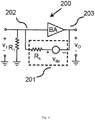
- FIG. 4 A second embodiment of the present invention shown in Fig. 4 in which the amplifier circuit 200 further includes a resistor R 1 .
- the input source 201 is represented as a Thevenin equivalent circuit with an input voltage source v IN and the source resistance R S .
- the voltage gain is determined by the ratio of resistors, which can be controlled more precisely and vary less due to process, temperature, or power supply voltage variations than the value of ⁇ in the first embodiment.
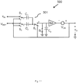
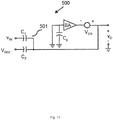
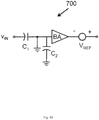
- FIG. 5 A third embodiment not forming part of the present invention is shown in Fig. 5 .
- the amplifier 300 performs discrete-time signal addition and amplification.
- the switches S0, S1 and S2 are operable to operate the circuit in two phases, namely a "sampling phase” and an "amplification phase.”
- the switch S0 is shown as a single-pole single-throw (SPST) switch and switches S1 and S2 are shown as single-pole double-throw (SPDT) switches having a common terminal C and respective output terminals 1 and 2.
- SPST single-pole single-throw
- SPDT single-pole double-throw
- Fig. 6 illustrates the circuit of Fig. 5 redrawn without the switches S0, S1 and S2 and showing the state of electrical connections during the sampling phase.
- the input voltage vIN is applied across the capacitor C1 and the reference voltage VREF is applied across the capacitor C2.
- the total charge Qtotal stored during the sampling phase on the capacitor plate 301 is given by -vIN C1-VREFC2.
- the switches are operated such that S0 is open, and the common terminal C of each of S1 and S2 is electrically coupled to terminal 2 of the switch.
- Fig. 7 illustrates the circuit of Fig. 5 redrawn without the switches S0, S1 and S2 and showing the state of electrical connections during the amplification phase.
- v O ⁇ 1 ⁇ ⁇ ⁇ C 1 v IN + C 2 V REF C 1 + C 2 ⁇ ⁇ 1 ⁇ C 1 v IN + C 2 V REF C 1 + C 2 which is amplification of the weighted sum of two voltages, v IN and V REF with a voltage gain of -1/ ⁇ .
- the weighting between the two voltages is given by the ratio of the two capacitors C 1 and C 2 .
- Such an operation is useful, for example, in an A/D converter.
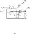
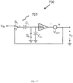
- FIG. 8 A fourth embodiment not forming part of the present invention is illustrated in Fig. 8 , where the amplifier circuit 400 includes a third capacitor C p , which may be parasitic capacitance or an intentional capacitance.
- the switches S 0 , S 1 and S 2 are operable to operate the circuit in two phases, namely a "sampling phase" and an "amplification phase.”
- the switch S 0 is shown as a single-pole single-throw (SPST) switch and switches S 1 and S 2 are shown as single-pole double-throw (SPDT) switches having a common terminal C and respective output terminals 1 and 2.
- SPST single-pole single-throw
- SPDT single-pole double-throw
- Fig. 9 illustrates the circuit of Fig. 8 redrawn without the switches S 0 , S 1 and S 2 and showing the state of electrical connections during the sampling phase.
- the input voltage v IN is applied across the capacitor C 1 and the reference voltage V REF is applied across the capacitor C 2 .
- the total charge Q total stored during the sampling phase on the capacitor plate 401 is given by - v IN C 1 -V REF C 2 .
- the switches are operated such that S 0 is open, and the common terminal C of each of S 1 and S 2 is electrically coupled to terminal 2 of the switch.
- Fig. 10 illustrates the circuit of Fig. 8 redrawn without the switches S 0 , S 1 and S 2 and showing the state of electrical connections during the amplification phase.
- Using the voltage v 1 at the input terminal of BA as the output yields substantially the same output voltage, and may be preferred in some applications.
- Buffers can exhibit an undesirable offset voltage.
- the output voltage is shifted by an offset voltage V OS from an ideal output voltage.
- Such an offset voltage is amplified by the amplifier circuit and produce an error at the output.
- the effect of an undesirable offset voltage V OS modeled as a voltage source in series of BA, is removed.
- the second capacitor C 2 may be parasitic capacitance or an intentional capacitance.
- the switches S 0 , S 1 , S 2 and S 3 are operable to operate the circuit in two phases, namely a "sampling phase" and an "amplification phase.”
- Fig. 11 the switches S 0 , S 1 , S 2 and S 3 are operable to operate the circuit in two phases, namely a "sampling phase" and an "amplification phase.”
- the switch S 0 is shown as a single-pole single-throw (SPST) switch and switches S 1 , S 2 and S 3 are shown as single-pole double-throw (SPDT) switches having a common terminal C and respective output terminals 1 and 2.
- SPST single-pole single-throw
- SPDT single-pole double-throw
- Fig. 12 illustrates the circuit of Fig. 11 redrawn without the switches S 0 , S 1 and S 2 and showing the state of electrical connections during the sampling phase.
- the input voltage v IN is applied across the capacitor C 1 and the reference voltage V REF is applied across the capacitor C 2 .
- the total charge Q total stored during the sampling phase on the capacitor plate 401 is given by - v IN C 1 -V REF C 2 .
- the switches are operated such that S 0 is open, and the common terminal C of each of S 1 , S 2 and S 3 is electrically coupled to terminal 2 of the switch.
- Fig. 13 illustrates the circuit of Fig.
- an intentional offset voltage V REF provided in the BA as represented by a voltage source V REF in series with the output of the BA.
- the offset can be introduced by a variety of methods, for example a base-to-emitter voltage V BE of an emitter follower, a gate-to-source voltage V GS of a source follower, or a capacitive level shifting.
- the amplifier 600 performs discrete-time signal amplification.
- the switches S 0 and S 1 are operable to operate the circuit in two phases, namely a "sampling phase” and an "amplification phase.”
- Fig. 14 For purposes of illustration, in Fig.
- the switch S 0 is shown as a single-pole single-throw (SPST) switch and switch S 2 is shown as a single-pole double-throw (SPDT) switch having a common terminal C and respective output terminals 1 and 2.
- SPST single-pole single-throw
- SPDT single-pole double-throw
- Fig. 15 illustrates the circuit of Fig. 14 redrawn without the switches S 0 and S 1 and showing the state of electrical connections during the sampling phase.
- the input voltage v IN is applied across the capacitor C 1 .
- the switches are operated such that S 0 is open, and the common terminal C of S 1 is electrically coupled to terminal 2 of the switch.
- Fig. 16 illustrates the circuit of Fig. 14 redrawn without the switches S 0 and S 1 and showing the state of electrical connections during the amplification phase.
- v O ⁇ 1 ⁇ ⁇ ⁇ v IN ⁇ V REF + V REF ⁇ ⁇ 1 ⁇ v IN ⁇ V REF + V REF
- the amplifier amplifies the difference between the input voltage and the offset voltage V REF by a voltage gain -1/ ⁇ .
- Fig. 18 illustrates the circuit of Fig. 17 redrawn without switches and showing the state of electrical connections during a sampling phase of circuit operation.
- Fig. 19 illustrates the circuit of Fig. 17 redrawn without switches and showing the state of electrical connections during an amplification phase of circuit operation.
- the buffer based amplification circuit 800 is used as a preamplifier for a comparator with two reference voltages, V REFN and V REFP .
- Such an arrangement can be used in flash analog-to-digital (A/D) converters and successive approximation register (SAR) A/D converters.
- the comparator typically consists of a latch (LATCH) or a preamplifier followed by a latch. Due to the device variability, a latch typically has a large random offset voltage, and is not suitable for ADC resolutions over 3-4 bits. Comparators for higher resolution ADCs generally employ a preamplifier in order to reduce the offset voltage. A potential drawback of such implementations is significant power consumption of the preamplifier.
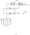
- An eighth embodiment not forming part of the present invention shown in Fig. 20 provides preamplification.
- Two buffer amplifiers, BA1 and BA2, and two capacitors, C1 and C2 are employed for a comparator.
- a latch 810 receives the output V OUT of the preamplifier.
- Fig. 21 illustrates the previous circuit without switches showing the state of electrical connections during the sampling phase.
- Fig. 22 illustrates the same circuit without the switches showing the state of electrical connections during the amplification phase.
- This amplified difference is applied to the latch 810, and the digital output Q of the latch is then applied to a logic circuit.
- the comparator typically consists of a latch or a preamplifier followed by a latch. Due to the device variability, a latch typically has a large random offset voltage, and is not suitable for ADC resolutions over 3-4 bits. Comparators for higher resolution ADCs generally employ a preamplifier in order to reduce the offset voltage. A drawback here is, again, the power consumption of the preamplifier.
- a SAR A/D converter 900 is provided two buffers, BA1 and BA2.
- a plurality of capacitors, C 1 , C 2 , through C N are appropriately ratioed for successive approximation.
- the the buffer based amplification is used as a preamplifier for comparators in flash analog-to-digital (A/D) converter.
- A/D flash analog-to-digital
- an input voltage V IN is compared with N tap voltages simultaneously by N comparators.
- the ninth embodiment not forming part of the present invention includes a voltage comparator preamplifier circuit 800 described in the eighth embodiment of the present invention for each voltage comparator in a flash A/D converter. Each comparator samples the input voltage during the sampling phase as described in the eighth embodiment.
- Fig. 25 shows A/D converter 900 without switches showing the state of electrical connections during the sampling phase.
- the input voltage v IN is sampled across C 1 , C 2 , through C N during the sampling phase of the operation.
- capacitors C 1 , C 2 , through C N are switched to the output of BA1 or BA2 according to the digital output Q of a latch 910 following a successive approximation algorithm.
- the output voltage V OUT is coupled to the latch 910 and the digital output Q of the latch is then applied to a SAR logic circuit, which controls the positions of the switches S 1 , S 2 , through S N .
- the switch S i is thrown to position 2 such that the corresponding capacitor C i is connected to the output voltage v OP of BA1
- the switch S i is thrown to position 3 such that the corresponding capacitor C i is connected to the output voltage v ON of BA2.
Description
- This application is directed to microelectronic circuits and circuit design and operation. More particularly, this application is directed to microelectronic amplifier circuits for use in semiconductor devices, integrated circuits and other electronic devices.
- Signal amplification is widely used in a variety of electronic systems. For example, in wireless communication systems, a low-noise amplifier (LNA) in the receiver amplifies the tiny signal picked up by an antenna. The amplified signal is then filtered, demodulated and further amplified again. The signal is often converted to a digital signal by an analog-to-digital converter. The analog-to-digital converter also typically amplifies the signal in the conversion process. In the transmitter, the power amplifier amplifies the radio frequency signal before the signal is transmitted through the antenna. In systems employing sensors, such as image sensors, microphones, and micro-electromechanical sensors, the signal produced by the sensors is very small, and thus must be amplified before further signal processing. There are numerous other places where signal amplification is required in a system. Conventional amplifier circuits fall into three general categories: a common-emitter amplifier (a common-source amplifier in MOS technologies), a common-based (a common-gate amplifier in MOS technologies),and an emitter-follower amplifier (a source-follower amplifier in MOS technologies). The first two types typically provide a substantial amount of voltage gain. However, the last type provides voltage gain that is close to one or slightly less, and as a result it has been suitable only as a buffer amplifier, but not as a voltage amplifier.
- The article Satomi Ogawa et al., "An Algorithmic Analog-to-Digital Converter Using Unity-Gain Buffers", published in IEEE Transaction on Instrumentation and Measurement, vol. 39, no. 6, 1. December 1990, pages 886-889 teaches a new circuit layout with minimum requirement for a bipolar 1-b A/D conversion using a unity gain buffer.
-
US7692471B2 teaches a switched capacitor circuit performing a two phase operation with a sampling phase and an amplification phase. At least two capacitors are switched to couple them across the input terminal and the output terminal of an amplifier during the amplification phase. - As an example of a simple circuit according to the prior art,
Fig. 1 provides an illustration of a representative common-source amplifier circuit 20 which operate in continuous-time. Thecircuit 20 also includes a MOSFET M1, and a load resistor R L. An analog input voltage v IN (hereafter referred to as "input voltage") provides an input to thecircuit 20, and a voltage v O (hereafter referred to as "output voltage") is provided as an output of thecircuit 20. The input voltage v IN generally includes a DC bias component V IN and a small-signal component vin (hereafter referred to as "input signal") such that v IN=V IN+v in. Likewise, the output voltage vO generally includes a DC component V O and a small-signal component v o (hereafter referred to as "output signal") such that v o =V O+v o . The DC components are required to bias the MOSFET in the desired region of operation. The small-signal components are typically the signals of interest. Thecircuit 20 amplifies the input signal vi such that the output signal v o is given by

- Further analysis of the
circuit 20 shows that the frequency f h where the magnitude of the voltage gain drops by 3 dB's from the low frequency value (hereafter referred to as "bandwidth") is given by
circuit 20, it is given by
- Applicants have recognized that substantial voltage amplification can be achieved with a buffer amplifier whose voltage gain is substantially equal to one, with the application including but not limited to signal amplification, voltage comparators, and A/D converters. In view of the foregoing, various preferred embodiments disclosed herein generally relate to an amplifier circuits having one or more buffer amplifiers and one or more resistors or one or more capacitors. Those skilled in the art will appreciate that the present concepts can be extended to other applications and circuits than the ones presented herein for the purpose of illustration. These and equivalent and similar circuits and techniques are intended to be covered by the scope of the appended claims.
- An embodiment is directed to an amplifier circuit operable in continuous-time. The amplifier circuit comprises: a buffer amplifier having an input terminal and an output terminal and an input source having a source resistance. The buffer amplifier has high input resistance and a voltage gain substantially equal to one, and the input source is electrically coupled across the input terminal and the output terminal of the buffer amplifier.
- Another embodiment is directed to an amplifier circuit operable in continuous-time with a voltage gain determined by a resistor ratio. The amplifier circuit comprises: a buffer amplifier having an input terminal and an output terminal, at least one resistor coupled to the input terminal of the buffer amplifier, and an input source having a source resistance. The buffer amplifier has high input resistance and a voltage gain substantially equal to one, and the input source is electrically coupled across the input terminal and the output terminal of the buffer amplifier.
- And another embodiment not forming part of the invention is directed to a discrete-time amplifier circuit operable in a sampling phase and an amplification phase to amplify a weighted sum of two input voltages. The amplifier circuit comprises a plurality of switches, a first and a second capacitor, and at least one buffer amplifier having an input terminal and an output terminal. During the sampling phase, the plurality of switches are configured to couple a first input voltage to the first capacitor and a second input voltage to the second capacitor. During the amplification phase, the plurality of switches are configured to couple the first and the second capacitors across the input terminal and the output terminal of the buffer amplifier to amplify a weighted sum of the first and the second input voltages.
- Yet another embodiment not forming part of the invention is directed to a discrete-time amplifier circuit operable in a sampling phase and an amplification phase to amplify a weighted sum of two input voltages without the adverse effect of an offset voltage of a buffer amplifier. The amplifier circuit comprises a plurality of switches, a first and a second capacitor, and at least one buffer amplifier having an input terminal and an output terminal. During the sampling phase, the plurality of switches are configured to couple a first input voltage and the output terminal of the buffer amplifier to the first capacitor and a second input voltage and the output terminal of the buffer amplifier to the second capacitor. During the amplification phase, the plurality of switches are configured to couple the first and the second capacitors across the input terminal and the output terminal of the buffer amplifier to amplify a weighted sum of the first and the second input voltages without the adverse effect of an offset voltage of the buffer amplifier.
- Still another embodiment not forming part of the invention is directed to a discrete-time amplifier circuit operable in a sampling phase and an amplification phase to amplify a difference between an input voltage and an intentional offset voltage of a buffer amplifier. The amplifier circuit comprises a plurality of switches, at least one capacitor, and a buffer amplifier having an input terminal and an output terminal. The buffer amplifier includes an intentional offset voltage, and the second capacitor is electrically coupled to the input terminal of the first buffer amplifier. During the sampling phase, the plurality of switches are configured to couple an input voltage to the first capacitor. During the amplification phase, the plurality of switches are configured to couple the at least one capacitor across the input terminal and the output terminal of the buffer amplifier to amplify a difference between the first input voltage and the first intentional offset voltage.
- An embodiment not forming part of the invention is directed to a discrete-time amplifier circuit operable in a sampling phase and an amplification phase to amplify a difference between an input voltage and intentional offset voltages of a plurality of buffer amplifiers. The amplifier circuit comprises a plurality of switches, a first, a second, and a third capacitor, and a first and a second buffer amplifier. The first buffer amplifier includes a first intentional offset voltage and the second buffer amplifier includes a second intentional offset voltage. The third capacitor is electrically coupled to the input terminal of the first buffer amplifier. During the sampling phase, the plurality of switches are configured to couple a first input voltage to the first and the second capacitor. During the amplification phase, the plurality of switches are configured to couple the first capacitor across the input terminal and the output terminal of the first buffer amplifier and the second capacitor across the input terminal and the output terminal of the first buffer amplifier.
- Another embodiment not forming part of the invention is directed to a flash analog-to-digital converter employing a buffer-based discrete-time amplifier circuit operable in a sampling phase and an amplification phase as a preamplifier for a voltage comparator. The analog-to-digital converter circuit comprises a plurality of switches, at least one capacitor, at least one buffer amplifier having an input terminal and an output terminal, and a latch circuit coupled to the input terminal of the buffer amplifier. During the sampling phase, the plurality of switches are configured to couple an input voltage to the at least one capacitor. During the amplification phase, the plurality of switches are configured to couple the at least one capacitor across the input terminal and the output terminal of the buffer amplifier.
- Yet another embodiment not forming part of the invention is directed to a successive approximation register analog-to-digital converter employing a buffer-based discrete-time amplifier circuit operable in a sampling phase and an amplification phase as a preamplifier for a voltage comparator. The analog-to-digital converter circuit comprises a plurality of switches, at least one capacitor, a first and a second buffer amplifier having an input terminal and an output terminal, and a latch circuit coupled to the input terminal of the first buffer amplifier. An output of the latch circuit is coupled to the plurality of switches. During the sampling phase, the plurality of switches are configured to couple an input voltage to the at least one capacitor. During the amplification phase, the plurality of switches are configured to couple the at least one capacitor across the input terminal and the output terminal of the first buffer amplifier or the second buffer amplifier depending on the digital output of the latch circuit.
- The appended drawings are provided to aid the understanding of the inventions and the following description of certain embodiments, and are to be considered as illustrative rather than limiting the scope of the inventive subject matter described herein. The drawings are not necessarily to scale; in some instances, various aspects of the inventive subject matter disclosed herein may be shown exaggerated or enlarged in the drawings to facilitate an understanding of different features. In the drawings, like reference characters generally refer to like features (e.g., functionally similar and/or structurally similar elements).
-
Fig. 1 provides an illustration of a prior art MOS common-source amplifier according to the prior art. -
Fig. 2 illustrates an amplifier circuit including a buffer amplifier, according to a first embodiment of the present invention. -
Fig. 3 illustrates the equivalent circuit ofFig. 2 . -
Fig. 4 illustrates an amplifier circuit including a buffer amplifier and a resistor, according to a second embodiment of the present invention. -
Fig. 5 illustrates a discrete-time amplifier circuit including a buffer amplifier and a plurality of capacitors, according to an embodiment not forming part of the present invention. -
Fig. 6 illustrates the circuit ofFig. 5 redrawn without switches and showing the state of electrical connections during a sampling phase of circuit operation. -
Fig. 7 illustrates the circuit ofFig. 5 redrawn without switches and showing the state of electrical connections during an amplification phase of circuit operation. -
Fig. 8 illustrates a discrete-time amplifier circuit including a buffer amplifier and plurality of capacitors, according to an embodiment not forming part of the present invention. -
Fig. 9 illustrates the circuit ofFig. 8 redrawn without switches and showing the state of electrical connections during a sampling phase of circuit operation. -
Fig. 10 illustrates the circuit ofFig. 8 redrawn without switches and showing the state of electrical connections during an amplification phase of circuit operation. -
Fig. 11 illustrates a discrete-time amplifier circuit including a buffer amplifier with an undesirable offset voltage and plurality of capacitors, according to an embodiment not forming part of the present invention. -
Fig. 12 illustrates the circuit ofFig. 11 redrawn without switches and showing the state of electrical connections during a sampling phase of circuit operation. -
Fig. 13 illustrates the circuit ofFig. 11 redrawn without switches and showing the state of electrical connections during an amplification phase of circuit operation. -
Fig. 14 illustrates a discrete-time amplifier circuit including a buffer amplifier with an intentional offset voltage and a capacitor, according to an embodiment not forming part of the present invention. -
Fig. 15 illustrates the circuit ofFig. 14 redrawn without switches and showing the state of electrical connections during a sampling phase of circuit operation. -
Fig. 16 illustrates the circuit ofFig. 14 redrawn without switches and showing the state of electrical connections during an amplification phase of circuit operation. -
Fig. 17 illustrates a discrete-time amplifier circuit including a buffer amplifier with an intentional offset voltage and plurality of capacitors, according to an embodiment not forming part of the present invention. -
Fig. 18 illustrates the circuit ofFig. 17 redrawn without switches and showing the state of electrical connections during a sampling phase of circuit operation. -
Fig. 19 illustrates the circuit ofFig. 17 redrawn without switches and showing the state of electrical connections during an amplification phase of circuit operation. -
Fig. 20 illustrates a discrete-time amplifier circuit including a plurality of buffer amplifiers each with an intentional offset voltage and plurality of capacitors, according to an embodiment not forming part of the present invention. -
Fig. 21 illustrates the circuit ofFig. 20 redrawn without switches and showing the state of electrical connections during a sampling phase of circuit operation. -
Fig. 22 illustrates the circuit ofFig. 20 redrawn without switches and showing the state of electrical connections during an amplification phase of circuit operation. -
Fig. 23 illustrates a prior art flash A/D converter. -
Fig. 24 illustrates a successive approximation register (SAR) A/D converter including a plurality of buffer amplifiers each with an intentional offset voltage and plurality of capacitors, according to an embodiment not forming part of the present invention. -
Fig. 25 illustrates the circuit ofFig. 24 redrawn without switches and showing the state of electrical connections during a sampling phase of circuit operation. -
Fig. 26 illustrates the circuit ofFig. 24 redrawn without switches and showing the state of electrical connections during a successive approximation phase of circuit operation. - The following description provides a discussion of various concepts related to, and embodiments of the present inventive apparatus and methods relating to signal amplification circuits. It should be appreciated that various concepts introduced above and discussed in greater detail below may be implemented in any of numerous ways, as the disclosed concepts are not limited to any particular manner of implementation. Examples of specific implementations and applications are provided primarily for illustrative purposes.
- Some aspects of the present invention provide a continuous-time amplifier topology based on a buffer amplifier (hereafter referred to as "buffer"). A buffer is an amplifier that provides a voltage gain substantially close to one as would be understood by those skilled in the art, while providing high input resistance and low output resistance. Those skilled in the art would also understand that a source-follower circuit or an emitter-follower circuit can be examples of a buffer.
- A first embodiment of the present invention is shown in
Fig. 2 . Theamplifier circuit 100 comprises a buffer amplifier BA, which may be a simple follower circuit such as an emitter follower or a source follower. A more sophisticated buffer such as an operational amplifier based buffer can also be employed for higher precision. Theinput source 101 is represented as a Thevenin equivalent circuit with an input voltage source v IN and the source resistance R S. Theinput source 101 is applied across theinput terminal 102 and theoutput terminal 103 of BA. - The equivalent circuit of the
amplifier circuit 100 according to the first embodiment is shown inFig. 3 . The buffer amplifier is modeled as a voltage controlled-voltage source with a voltage gain (1-ε) where ε is typically much less than unity (<<1), and an output resistance R o. Since the input resistance of BA is high, it is modeled as an open-circuit inFig. 3 . Therefore, the current i l into the amplifier is zero. Hence, the current through the output resistance R o and the source resistance R s is also zero, giving;

- Combining the above two equations, the output voltage v O of the
amplifier 100 is found to be
- Thus voltage gain of the
amplifier 100 is given by;
- In a typical buffer, ε is small, thus the voltage gain a v is large.
- The output resistance of the
amplifier 100 according to the first embodiment is shown to be
- For certain applications, it may be more convenient to use the input voltage of BA v 1 as the output voltage. In this case, the voltage gain is given by

- Further analysis of the
amplifier 100 shows that the bandwidth is given by

prior art amplifier 20. Thus, the first embodiment of the present invention provides an new amplifier configuration with the same figure of merit as aprior art amplifier 20. - A second embodiment of the present invention shown in
Fig. 4 in which theamplifier circuit 200 further includes a resistor R 1. Theinput source 201 is represented as a Thevenin equivalent circuit with an input voltage source v IN and the source resistance R S. Theinput source 201 is applied across theinput terminal 202 and theoutput 203 terminal of BA. It can be shown that for ε<<1, the voltage gain of the amplifier is approximated by
- The above equation indicates that the voltage gain is determined by the ratio of resistors, which can be controlled more precisely and vary less due to process, temperature, or power supply voltage variations than the value of ε in the first embodiment.
- A third embodiment not forming part of the present invention is shown in
Fig. 5 . Theamplifier 300 performs discrete-time signal addition and amplification. In the circuit ofFig. 5 the switches S0, S1 and S2 are operable to operate the circuit in two phases, namely a "sampling phase" and an "amplification phase." For purposes of illustration, inFig. 5 the switch S0 is shown as a single-pole single-throw (SPST) switch and switches S1 and S2 are shown as single-pole double-throw (SPDT) switches having a common terminal C andrespective output terminals Fig. 5 , i.e., S0 closed and the common terminal C of each of S1 and S2 is electrically coupled toterminal 1 of the switch. -
Fig. 6 illustrates the circuit ofFig. 5 redrawn without the switches S0, S1 and S2 and showing the state of electrical connections during the sampling phase. As shown inFig. 6 , the input voltage vIN is applied across the capacitor C1 and the reference voltage VREF is applied across the capacitor C2. Thus, the total charge Qtotal stored during the sampling phase on thecapacitor plate 301 is given by -vIN C1-VREFC2. During the amplification phase, the switches are operated such that S0 is open, and the common terminal C of each of S1 and S2 is electrically coupled toterminal 2 of the switch. -
Fig. 7 illustrates the circuit ofFig. 5 redrawn without the switches S0, S1 and S2 and showing the state of electrical connections during the amplification phase. In the amplification phase, because charge is conserved oncapacitor plate 301,
- Solving for the output voltage v O:

- For some applications, it may be more convenient to use the input voltage of the buffer v 1 as the output voltage. In this case, the output voltage is also given by

- A fourth embodiment not forming part of the present invention is illustrated in
Fig. 8 , where theamplifier circuit 400 includes a third capacitor C p, which may be parasitic capacitance or an intentional capacitance. As would be readily appreciated by one of skill in the art, in the circuit ofFig. 8 the switches S0, S1 and S2 are operable to operate the circuit in two phases, namely a "sampling phase" and an "amplification phase." For purposes of illustration, inFig. 8 the switch S0 is shown as a single-pole single-throw (SPST) switch and switches S1 and S2 are shown as single-pole double-throw (SPDT) switches having a common terminal C andrespective output terminals Fig. 8 , i.e., S0 closed and the common terminal C of each of S1 and S2 is electrically coupled toterminal 1 of the switch. -
Fig. 9 illustrates the circuit ofFig. 8 redrawn without the switches S0, S1 and S2 and showing the state of electrical connections during the sampling phase. As shown inFig. 8 , the input voltage v IN is applied across the capacitor C 1 and the reference voltage V REF is applied across the capacitor C 2. Thus, the total charge Q total stored during the sampling phase on thecapacitor plate 401 is given by -v IN C 1-VREF C 2. During the amplification phase, the switches are operated such that S0 is open, and the common terminal C of each of S1 and S2 is electrically coupled toterminal 2 of the switch. -
Fig. 10 illustrates the circuit ofFig. 8 redrawn without the switches S0, S1 and S2 and showing the state of electrical connections during the amplification phase. In the amplification phase, because charge is conserved,
- Assuming the gain of the buffer is very close to 1, i.e. ε<<1, and solving for the output voltage v O


- Using the voltage v 1 at the input terminal of BA as the output yields substantially the same output voltage, and may be preferred in some applications.
- Buffers can exhibit an undesirable offset voltage. In other words, the output voltage is shifted by an offset voltage V OS from an ideal output voltage. Such an offset voltage is amplified by the amplifier circuit and produce an error at the output. In a fifth embodiment not forming part of the present invention shown in
Fig. 11 , the effect of an undesirable offset voltage V OS, modeled as a voltage source in series of BA, is removed. The second capacitor C 2 may be parasitic capacitance or an intentional capacitance. In the circuit ofFig. 11 the switches S0, S1, S2 and S3 are operable to operate the circuit in two phases, namely a "sampling phase" and an "amplification phase." For purposes of illustration, inFig. 11 the switch S0 is shown as a single-pole single-throw (SPST) switch and switches S1, S2 and S3 are shown as single-pole double-throw (SPDT) switches having a common terminal C andrespective output terminals Fig. 11 , i.e., S0 closed and the common terminal C of each of S1, S2 and S3 is electrically coupled toterminal 1 of the switch. -
Fig. 12 illustrates the circuit ofFig. 11 redrawn without the switches S0, S1 and S2 and showing the state of electrical connections during the sampling phase. As shown inFig. 11 , the input voltage v IN is applied across the capacitor C 1 and the reference voltage V REF is applied across the capacitor C 2. Thus, the total charge Q total stored during the sampling phase on thecapacitor plate 401 is given by -v IN C 1-VREF C 2. During the amplification phase, the switches are operated such that S0 is open, and the common terminal C of each of S1, S2 and S3 is electrically coupled toterminal 2 of the switch.Fig. 13 illustrates the circuit ofFig. 11 redrawn without the switches S0, S1, S2 and S3 and showing the state of electrical connections during the amplification phase. Assuming the gain of the buffer is very close to 1, i.e. ε<<1, and using v 1 as the output, it can be shown that
- In a sixth embodiment not forming part of the present invention, shown in
Fig. 14 , an intentional offset voltage VREF provided in the BA, as represented by a voltage source VREF in series with the output of the BA. The offset can be introduced by a variety of methods, for example a base-to-emitter voltage V BE of an emitter follower, a gate-to-source voltage V GS of a source follower, or a capacitive level shifting. Theamplifier 600 performs discrete-time signal amplification. In the circuit ofFig. 14 the switches S0 and S1 are operable to operate the circuit in two phases, namely a "sampling phase" and an "amplification phase." For purposes of illustration, inFig. 14 the switch S0 is shown as a single-pole single-throw (SPST) switch and switch S2 is shown as a single-pole double-throw (SPDT) switch having a common terminal C andrespective output terminals Fig. 14 , i.e., S0 closed and the common terminal C of S1 is electrically coupled toterminal 1 of the switch. -
Fig. 15 illustrates the circuit ofFig. 14 redrawn without the switches S0 and S1 and showing the state of electrical connections during the sampling phase. As shown inFig. 15 , the input voltage vIN is applied across the capacitor C 1. During the amplification phase, the switches are operated such that S0 is open, and the common terminal C of S1 is electrically coupled toterminal 2 of the switch.Fig. 16 illustrates the circuit ofFig. 14 redrawn without the switches S0 and S1 and showing the state of electrical connections during the amplification phase. - It can be shown that the voltage at the output of the BA in the amplification phase is given by

- In some applications, it may be desirable to use the input voltage v 1 as the output voltage. In this case, the output voltage is given by

- Thus, the amplifier amplifies the difference between the input voltage and the offset voltage V REF by a voltage gain -1/ε.
- In a seventh embodiment not forming part of the present invention shown in
Fig. 17 , the buffer BA is provided with an intentional offset voltage VREF, and a capacitor C 2 further included, which can be either intentional capacitance or parasitic capacitance. It can be shown that for ε<<1, the output voltage in the amplification phase of the amplifier is given by
output 
- Thus, the difference between the input voltage vIN and the offset voltage VREF is amplified by a voltage gain av determined by the ratio of capacitors C 1 and C 2;

-
Fig. 18 illustrates the circuit ofFig. 17 redrawn without switches and showing the state of electrical connections during a sampling phase of circuit operation. -
Fig. 19 illustrates the circuit ofFig. 17 redrawn without switches and showing the state of electrical connections during an amplification phase of circuit operation. - In an eighth embodiment not forming part of the present invention, shown in
Fig. 20 , the buffer basedamplification circuit 800 is used as a preamplifier for a comparator with two reference voltages, VREFN and VREFP. Such an arrangement can be used in flash analog-to-digital (A/D) converters and successive approximation register (SAR) A/D converters. - The comparator typically consists of a latch (LATCH) or a preamplifier followed by a latch. Due to the device variability, a latch typically has a large random offset voltage, and is not suitable for ADC resolutions over 3-4 bits. Comparators for higher resolution ADCs generally employ a preamplifier in order to reduce the offset voltage. A potential drawback of such implementations is significant power consumption of the preamplifier.
- An eighth embodiment not forming part of the present invention shown in
Fig. 20 provides preamplification. Two buffer amplifiers, BA1 and BA2, and two capacitors, C1 and C2 are employed for a comparator. Alatch 810 receives the output V OUT of the preamplifier. BA1 and BA2 are buffers with appropriate offsets provided. For example, the offset VREFP of BA1 and VREFN of BA2, where V REFP-V REFN=V REF. -
Fig. 21 illustrates the previous circuit without switches showing the state of electrical connections during the sampling phase.Fig. 22 illustrates the same circuit without the switches showing the state of electrical connections during the amplification phase. Assuming ε<<1 for both BA1 and BA2, the output voltage VOUT in the amplification phase is


- This amplified difference is applied to the
latch 810, and the digital output Q of the latch is then applied to a logic circuit. - A prior art flash A/D converter is shown in
Fig. 23 , where a resistor ladder produces the tap voltages that are compared with the input voltage by a bank of N comparators. With the top of the ladder connected to one reference voltage VREFP and the bottom of the reference connected to another reference voltage VREFN, the voltage at the k-th tap from the bottom is given by;
- The comparator typically consists of a latch or a preamplifier followed by a latch. Due to the device variability, a latch typically has a large random offset voltage, and is not suitable for ADC resolutions over 3-4 bits. Comparators for higher resolution ADCs generally employ a preamplifier in order to reduce the offset voltage. A drawback here is, again, the power consumption of the preamplifier. A preamplifier amplifies the difference between the input voltage V IN and the tap voltage V k by a voltage gain a, producing an output voltage;

- In a ninth embodiment not forming part of the present invention, shown in
Fig. 24 , a SAR A/D converter 900 is provided two buffers, BA1 and BA2. A plurality of capacitors, C 1, C 2, through C N, are appropriately ratioed for successive approximation. The the buffer based amplification is used as a preamplifier for comparators in flash analog-to-digital (A/D) converter. In a flash A/D converter, an input voltage V IN is compared with N tap voltages simultaneously by N comparators. - The ninth embodiment not forming part of the present invention includes a voltage
comparator preamplifier circuit 800 described in the eighth embodiment of the present invention for each voltage comparator in a flash A/D converter. Each comparator samples the input voltage during the sampling phase as described in the eighth embodiment. The output voltage V OUT of thecircuit 800 in the amplification phase is


- Thus, by choosing an appropriate ratio between C 1 and C 2, an effective tap voltage is created, and an output voltage that is equivalent to the output voltage of a prior art preamplifier is produced, without the use of the resistor ladder. The digital output Q of the latch is then applied to an encoding logic circuit.
-
Fig. 25 shows A/D converter 900 without switches showing the state of electrical connections during the sampling phase. The input voltage v IN is sampled across C 1, C 2, through C N during the sampling phase of the operation. During the subsequent successive approximation phases, shown inFig. 26 without the switches for simplicity, capacitors C 1, C 2, through C N are switched to the output of BA1 or BA2 according to the digital output Q of alatch 910 following a successive approximation algorithm. The output voltage V OUT is coupled to thelatch 910 and the digital output Q of the latch is then applied to a SAR logic circuit, which controls the positions of the switches S 1, S 2, through S N. More specifically, if the i-th digital output code of the latch 910 D i (i=1,2, k, ... N) is 1, the switch Si is thrown toposition 2 such that the corresponding capacitor Ci is connected to the output voltage vOP of BA1, if the i-th digital code D i is 0, the switch Si is thrown toposition 3 such that the corresponding capacitor C i is connected to the output voltage vON of BA2. This operation produces an output voltage


- It is shown that the output voltage is identical to that of a preamplifier output in a prior art successive approximation ADC with a voltage gain a v. Since a reference buffer is generally required for each of the reference voltages in a prior art A/D converter, BA1 and BA2 may be created by slight modifications of these reference buffers. Therefore, an effective preamplification is achieved without a significant increase in complexity or power consumption.
- Although the exemplary embodiments described in the previous herein have been illustrated in single-ended topologies, the extension to fully-differential topologies are straightforward. Also, a ground voltage is indicated in these embodiments for simplicity of explanation. The ground voltage can be replaced by a system common-mode voltage VCM in actual circuits without affecting the functionality of the embodiments.
Claims (5)
- A continuous-time amplifier circuit (100) comprising:a buffer amplifier (BA) having an input terminal (102) and an output terminal (103); andan input source (101) configured to be represented as a Thevenin equivalent circuit comprising an input voltage source in series with a source resistance (Rs) for supplying an input voltage (vIN) including a DC bias component (VIN) and a small signal component as an input signal (vin) to the circuit (100):wherein the buffer amplifier (BA) is adapted as a voltage controlled-voltage source having an input resistance as an open circuit and a voltage gain equal to 1-ε, where ε<<1; andthe input source (101) is electrically coupled across the input terminal (102) and the output terminal (103) of the buffer amplifier (BA).
- The circuit of claim 1, further including a resistor (Ri) electrically coupled to the input terminal of the buffer amplifier.
- The circuit of claim 1, wherein a voltage gain av provided by the ratio among the voltages at the input and the output terminals has a value with an inverse dependency with respect to ε.
- The circuit of claim 3, wherein an output voltage (Vo) is obtained at the output terminal of the buffer amplifier and the gain equals (1-ε)/ε.
- The circuit of claim 3, wherein an output voltage is obtained at the input terminal of the buffer amplifier and the gain equals 1/ε.
Priority Applications (1)
| Application Number | Priority Date | Filing Date | Title |
|---|---|---|---|
| EP19181157.9A EP3576301B1 (en) | 2013-03-15 | 2014-03-14 | Buffer amplifier circuit |
Applications Claiming Priority (2)
| Application Number | Priority Date | Filing Date | Title |
|---|---|---|---|
| US201361791911P | 2013-03-15 | 2013-03-15 | |
| PCT/US2014/027303 WO2014152402A2 (en) | 2013-03-15 | 2014-03-14 | Buffer amplifier circuit |
Related Child Applications (2)
| Application Number | Title | Priority Date | Filing Date |
|---|---|---|---|
| EP19181157.9A Division EP3576301B1 (en) | 2013-03-15 | 2014-03-14 | Buffer amplifier circuit |
| EP19181157.9A Division-Into EP3576301B1 (en) | 2013-03-15 | 2014-03-14 | Buffer amplifier circuit |
Publications (3)
| Publication Number | Publication Date |
|---|---|
| EP2974008A2 EP2974008A2 (en) | 2016-01-20 |
| EP2974008A4 EP2974008A4 (en) | 2016-09-07 |
| EP2974008B1 true EP2974008B1 (en) | 2021-01-27 |
Family
ID=51525158
Family Applications (2)
| Application Number | Title | Priority Date | Filing Date |
|---|---|---|---|
| EP14768045.8A Active EP2974008B1 (en) | 2013-03-15 | 2014-03-14 | Buffer amplifier circuit |
| EP19181157.9A Active EP3576301B1 (en) | 2013-03-15 | 2014-03-14 | Buffer amplifier circuit |
Family Applications After (1)
| Application Number | Title | Priority Date | Filing Date |
|---|---|---|---|
| EP19181157.9A Active EP3576301B1 (en) | 2013-03-15 | 2014-03-14 | Buffer amplifier circuit |
Country Status (4)
| Country | Link |
|---|---|
| US (2) | US9154089B2 (en) |
| EP (2) | EP2974008B1 (en) |
| CN (1) | CN105247783B (en) |
| WO (1) | WO2014152402A2 (en) |
Families Citing this family (5)
| Publication number | Priority date | Publication date | Assignee | Title |
|---|---|---|---|---|
| CN107251436B (en) | 2015-02-24 | 2021-08-06 | 欧姆尼设计技术有限公司 | Differential switched capacitor circuit with voltage amplifier and associated method |
| US10812027B2 (en) | 2017-05-26 | 2020-10-20 | 2Pai Semiconductor Co., Limited | Isolation circuit |
| WO2019203993A1 (en) * | 2018-04-18 | 2019-10-24 | Rambus Inc. | Serial-link receiver using time-interleaved discrete time gain |
| US10771280B1 (en) * | 2019-02-20 | 2020-09-08 | Texas Instruments Incorporated | Low-power wake-up circuit for controller area network (CAN) transceiver |
| US11418210B2 (en) * | 2020-05-05 | 2022-08-16 | Omni Design Technologies, Inc. | Digital-to-analog converter with reference voltage selection switch |
Family Cites Families (17)
| Publication number | Priority date | Publication date | Assignee | Title |
|---|---|---|---|---|
| US4763106A (en) | 1987-07-20 | 1988-08-09 | Zdzislaw Gulczynski | Flash analog-to-digital converter |
| JPH0734541B2 (en) * | 1987-07-27 | 1995-04-12 | 日本電気株式会社 | Successive approximation type analog-digital conversion system |
| FR2657719B1 (en) * | 1990-01-30 | 1994-08-26 | Thomson Composants Militaires | SAMPLING CIRCUIT FOR ANALOG SIGNALS. |
| EP0509585A1 (en) * | 1991-04-15 | 1992-10-21 | Koninklijke Philips Electronics N.V. | Clocked comparator with offset-voltage compensation |
| JPH0645875A (en) * | 1992-07-24 | 1994-02-18 | Nec Corp | Switched capacitor circuit |
| JP2644191B2 (en) * | 1994-08-04 | 1997-08-25 | 日本電気エンジニアリング株式会社 | Buffer amplifier |
| JP2708007B2 (en) * | 1995-03-31 | 1998-02-04 | 日本電気株式会社 | Sample and hold circuit |
| US5574457A (en) * | 1995-06-12 | 1996-11-12 | Motorola, Inc. | Switched capacitor gain stage |
| FI120124B (en) * | 1998-05-29 | 2009-06-30 | Nokia Corp | A method and circuit for sampling a signal at a high sampling rate |
| US6452531B1 (en) | 1999-08-27 | 2002-09-17 | Analog Devices, Inc. | Jitter and load insensitive charge transfer |
| US6992509B2 (en) | 2003-10-02 | 2006-01-31 | Supertex, Inc. | Switched-capacitor sample/hold having reduced amplifier slew-rate and settling time requirements |
| JP2006086981A (en) * | 2004-09-17 | 2006-03-30 | Fujitsu Ltd | Switched capacitor circuit and pipeline a/d conversion circuit |
| US7113116B2 (en) * | 2005-01-26 | 2006-09-26 | Analog Devices, Inc. | Sample and hold apparatus |
| JP4195500B1 (en) * | 2008-01-22 | 2008-12-10 | 有限会社リニアセル・デザイン | Switched capacitor amplifier circuit |
| CN102545900B (en) * | 2010-12-20 | 2015-05-20 | 意法半导体研发(上海)有限公司 | Analog/digital (A/D) conversion system and method |
| WO2014059437A2 (en) | 2012-10-12 | 2014-04-17 | Hae LEE | Switched capacitor circuits having level-shifting buffer amplifiers, and associated methods |
| US8823572B2 (en) * | 2012-12-17 | 2014-09-02 | Dust Networks, Inc. | Anti-aliasing sampling circuits and analog-to-digital converter |
-
2014
- 2014-03-14 EP EP14768045.8A patent/EP2974008B1/en active Active
- 2014-03-14 EP EP19181157.9A patent/EP3576301B1/en active Active
- 2014-03-14 WO PCT/US2014/027303 patent/WO2014152402A2/en active Application Filing
- 2014-03-14 US US14/210,958 patent/US9154089B2/en active Active
- 2014-03-14 CN CN201480027520.XA patent/CN105247783B/en active Active
-
2015
- 2015-05-27 US US14/723,044 patent/US9356565B2/en active Active
Non-Patent Citations (1)
| Title |
|---|
| None * |
Also Published As
| Publication number | Publication date |
|---|---|
| WO2014152402A3 (en) | 2014-11-13 |
| US9356565B2 (en) | 2016-05-31 |
| EP3576301B1 (en) | 2024-02-28 |
| US20150280658A1 (en) | 2015-10-01 |
| CN105247783A (en) | 2016-01-13 |
| EP2974008A2 (en) | 2016-01-20 |
| US20140266845A1 (en) | 2014-09-18 |
| WO2014152402A2 (en) | 2014-09-25 |
| CN105247783B (en) | 2018-02-27 |
| US9154089B2 (en) | 2015-10-06 |
| EP3576301A1 (en) | 2019-12-04 |
| EP2974008A4 (en) | 2016-09-07 |
Similar Documents
| Publication | Publication Date | Title |
|---|---|---|
| US9391628B1 (en) | Low noise precision input stage for analog-to-digital converters | |
| US8330537B1 (en) | Low noise, high CMRR and PSRR input buffer | |
| EP2974008B1 (en) | Buffer amplifier circuit | |
| US7358801B2 (en) | Reducing noise and/or power consumption in a switched capacitor amplifier sampling a reference voltage | |
| CN104423409B (en) | Closed loop control system, and an amplifier in combination with such a closed loop control system | |
| US9667194B2 (en) | Differential switched capacitor circuits having voltage amplifiers, and associated methods | |
| US8232905B2 (en) | Sequentially configured analog to digital converter | |
| US7417574B2 (en) | Efficient amplifier sharing in a multi-stage analog to digital converter | |
| US7385426B1 (en) | Low current offset integrator with signal independent low input capacitance buffer circuit | |
| US7898331B2 (en) | Increasing the common mode range of a circuit | |
| US6970124B1 (en) | Inherent-offset comparator and converter systems | |
| US9866236B1 (en) | Appapatus and method for fast conversion, compact, ultra low power, wide supply range auxiliary digital to analog converters | |
| US20160329881A1 (en) | Amplifying circuit | |
| KR101236977B1 (en) | Apparatus for detecting current for multi sensor arrays | |
| Chandrashekar et al. | A 20-MS/s to 40-MS/s reconfigurable pipeline ADC implemented with parallel OTA scaling | |
| US8456337B1 (en) | System to interface analog-to-digital converters to inputs with arbitrary common-modes | |
| US20140000364A1 (en) | Hybrid analog to digital converter and sensing apparatus using the same | |
| Bindra et al. | Range pre-selection sampling technique to reduce input drive energy for SAR ADCs | |
| US9350306B2 (en) | Amplification circuit, amplification device, AFE circuit, and signal processing system | |
| US11309903B1 (en) | Sampling network with dynamic voltage detector for delay output | |
| US11451237B2 (en) | Sample and hold circuit and method | |
| US11533060B2 (en) | Multipath sampling circuits | |
| CN108512550B (en) | Differential sampling circuit | |
| CN116865729A (en) | Comparator, analog-to-digital converter and electronic equipment | |
| US20190058466A1 (en) | Electronic circuit and control method for electronic circuit |
Legal Events
| Date | Code | Title | Description |
|---|---|---|---|
| PUAI | Public reference made under article 153(3) epc to a published international application that has entered the european phase |
Free format text: ORIGINAL CODE: 0009012 |
|
| 17P | Request for examination filed |
Effective date: 20151015 |
|
| AK | Designated contracting states |
Kind code of ref document: A2 Designated state(s): AL AT BE BG CH CY CZ DE DK EE ES FI FR GB GR HR HU IE IS IT LI LT LU LV MC MK MT NL NO PL PT RO RS SE SI SK SM TR |
|
| AX | Request for extension of the european patent |
Extension state: BA ME |
|
| DAX | Request for extension of the european patent (deleted) | ||
| A4 | Supplementary search report drawn up and despatched |
Effective date: 20160805 |
|
| RIC1 | Information provided on ipc code assigned before grant |
Ipc: H03M 1/46 20060101ALI20160801BHEP Ipc: H03F 3/70 20060101ALI20160801BHEP Ipc: H03F 3/62 20060101ALI20160801BHEP Ipc: H03F 3/16 20060101AFI20160801BHEP Ipc: H03M 1/14 20060101ALI20160801BHEP |
|
| STAA | Information on the status of an ep patent application or granted ep patent |
Free format text: STATUS: EXAMINATION IS IN PROGRESS |
|
| 17Q | First examination report despatched |
Effective date: 20170418 |
|
| GRAP | Despatch of communication of intention to grant a patent |
Free format text: ORIGINAL CODE: EPIDOSNIGR1 |
|
| STAA | Information on the status of an ep patent application or granted ep patent |
Free format text: STATUS: GRANT OF PATENT IS INTENDED |
|
| INTG | Intention to grant announced |
Effective date: 20201102 |
|
| GRAS | Grant fee paid |
Free format text: ORIGINAL CODE: EPIDOSNIGR3 |
|
| GRAA | (expected) grant |
Free format text: ORIGINAL CODE: 0009210 |
|
| STAA | Information on the status of an ep patent application or granted ep patent |
Free format text: STATUS: THE PATENT HAS BEEN GRANTED |
|
| AK | Designated contracting states |
Kind code of ref document: B1 Designated state(s): AL AT BE BG CH CY CZ DE DK EE ES FI FR GB GR HR HU IE IS IT LI LT LU LV MC MK MT NL NO PL PT RO RS SE SI SK SM TR |
|
| REG | Reference to a national code |
Ref country code: GB Ref legal event code: FG4D |
|
| REG | Reference to a national code |
Ref country code: CH Ref legal event code: EP |
|
| REG | Reference to a national code |
Ref country code: AT Ref legal event code: REF Ref document number: 1359245 Country of ref document: AT Kind code of ref document: T Effective date: 20210215 |
|
| REG | Reference to a national code |
Ref country code: IE Ref legal event code: FG4D |
|
| REG | Reference to a national code |
Ref country code: DE Ref legal event code: R096 Ref document number: 602014074571 Country of ref document: DE |
|
| REG | Reference to a national code |
Ref country code: NL Ref legal event code: MP Effective date: 20210127 |
|
| REG | Reference to a national code |
Ref country code: LT Ref legal event code: MG9D |
|
| REG | Reference to a national code |
Ref country code: AT Ref legal event code: MK05 Ref document number: 1359245 Country of ref document: AT Kind code of ref document: T Effective date: 20210127 |
|
| PG25 | Lapsed in a contracting state [announced via postgrant information from national office to epo] |
Ref country code: GR Free format text: LAPSE BECAUSE OF FAILURE TO SUBMIT A TRANSLATION OF THE DESCRIPTION OR TO PAY THE FEE WITHIN THE PRESCRIBED TIME-LIMIT Effective date: 20210428 Ref country code: FI Free format text: LAPSE BECAUSE OF FAILURE TO SUBMIT A TRANSLATION OF THE DESCRIPTION OR TO PAY THE FEE WITHIN THE PRESCRIBED TIME-LIMIT Effective date: 20210127 Ref country code: HR Free format text: LAPSE BECAUSE OF FAILURE TO SUBMIT A TRANSLATION OF THE DESCRIPTION OR TO PAY THE FEE WITHIN THE PRESCRIBED TIME-LIMIT Effective date: 20210127 Ref country code: PT Free format text: LAPSE BECAUSE OF FAILURE TO SUBMIT A TRANSLATION OF THE DESCRIPTION OR TO PAY THE FEE WITHIN THE PRESCRIBED TIME-LIMIT Effective date: 20210527 Ref country code: LT Free format text: LAPSE BECAUSE OF FAILURE TO SUBMIT A TRANSLATION OF THE DESCRIPTION OR TO PAY THE FEE WITHIN THE PRESCRIBED TIME-LIMIT Effective date: 20210127 Ref country code: BG Free format text: LAPSE BECAUSE OF FAILURE TO SUBMIT A TRANSLATION OF THE DESCRIPTION OR TO PAY THE FEE WITHIN THE PRESCRIBED TIME-LIMIT Effective date: 20210427 Ref country code: NO Free format text: LAPSE BECAUSE OF FAILURE TO SUBMIT A TRANSLATION OF THE DESCRIPTION OR TO PAY THE FEE WITHIN THE PRESCRIBED TIME-LIMIT Effective date: 20210427 Ref country code: NL Free format text: LAPSE BECAUSE OF FAILURE TO SUBMIT A TRANSLATION OF THE DESCRIPTION OR TO PAY THE FEE WITHIN THE PRESCRIBED TIME-LIMIT Effective date: 20210127 |
|
| PG25 | Lapsed in a contracting state [announced via postgrant information from national office to epo] |
Ref country code: SE Free format text: LAPSE BECAUSE OF FAILURE TO SUBMIT A TRANSLATION OF THE DESCRIPTION OR TO PAY THE FEE WITHIN THE PRESCRIBED TIME-LIMIT Effective date: 20210127 Ref country code: RS Free format text: LAPSE BECAUSE OF FAILURE TO SUBMIT A TRANSLATION OF THE DESCRIPTION OR TO PAY THE FEE WITHIN THE PRESCRIBED TIME-LIMIT Effective date: 20210127 Ref country code: LV Free format text: LAPSE BECAUSE OF FAILURE TO SUBMIT A TRANSLATION OF THE DESCRIPTION OR TO PAY THE FEE WITHIN THE PRESCRIBED TIME-LIMIT Effective date: 20210127 Ref country code: PL Free format text: LAPSE BECAUSE OF FAILURE TO SUBMIT A TRANSLATION OF THE DESCRIPTION OR TO PAY THE FEE WITHIN THE PRESCRIBED TIME-LIMIT Effective date: 20210127 Ref country code: AT Free format text: LAPSE BECAUSE OF FAILURE TO SUBMIT A TRANSLATION OF THE DESCRIPTION OR TO PAY THE FEE WITHIN THE PRESCRIBED TIME-LIMIT Effective date: 20210127 |
|
| PG25 | Lapsed in a contracting state [announced via postgrant information from national office to epo] |
Ref country code: IS Free format text: LAPSE BECAUSE OF FAILURE TO SUBMIT A TRANSLATION OF THE DESCRIPTION OR TO PAY THE FEE WITHIN THE PRESCRIBED TIME-LIMIT Effective date: 20210527 |
|
| REG | Reference to a national code |
Ref country code: DE Ref legal event code: R097 Ref document number: 602014074571 Country of ref document: DE |
|
| PG25 | Lapsed in a contracting state [announced via postgrant information from national office to epo] |
Ref country code: SM Free format text: LAPSE BECAUSE OF FAILURE TO SUBMIT A TRANSLATION OF THE DESCRIPTION OR TO PAY THE FEE WITHIN THE PRESCRIBED TIME-LIMIT Effective date: 20210127 Ref country code: EE Free format text: LAPSE BECAUSE OF FAILURE TO SUBMIT A TRANSLATION OF THE DESCRIPTION OR TO PAY THE FEE WITHIN THE PRESCRIBED TIME-LIMIT Effective date: 20210127 Ref country code: CZ Free format text: LAPSE BECAUSE OF FAILURE TO SUBMIT A TRANSLATION OF THE DESCRIPTION OR TO PAY THE FEE WITHIN THE PRESCRIBED TIME-LIMIT Effective date: 20210127 Ref country code: MC Free format text: LAPSE BECAUSE OF FAILURE TO SUBMIT A TRANSLATION OF THE DESCRIPTION OR TO PAY THE FEE WITHIN THE PRESCRIBED TIME-LIMIT Effective date: 20210127 |
|
| REG | Reference to a national code |
Ref country code: CH Ref legal event code: PL |
|
| PG25 | Lapsed in a contracting state [announced via postgrant information from national office to epo] |
Ref country code: ES Free format text: LAPSE BECAUSE OF FAILURE TO SUBMIT A TRANSLATION OF THE DESCRIPTION OR TO PAY THE FEE WITHIN THE PRESCRIBED TIME-LIMIT Effective date: 20210127 Ref country code: DK Free format text: LAPSE BECAUSE OF FAILURE TO SUBMIT A TRANSLATION OF THE DESCRIPTION OR TO PAY THE FEE WITHIN THE PRESCRIBED TIME-LIMIT Effective date: 20210127 Ref country code: SK Free format text: LAPSE BECAUSE OF FAILURE TO SUBMIT A TRANSLATION OF THE DESCRIPTION OR TO PAY THE FEE WITHIN THE PRESCRIBED TIME-LIMIT Effective date: 20210127 Ref country code: RO Free format text: LAPSE BECAUSE OF FAILURE TO SUBMIT A TRANSLATION OF THE DESCRIPTION OR TO PAY THE FEE WITHIN THE PRESCRIBED TIME-LIMIT Effective date: 20210127 |
|
| PLBE | No opposition filed within time limit |
Free format text: ORIGINAL CODE: 0009261 |
|
| STAA | Information on the status of an ep patent application or granted ep patent |
Free format text: STATUS: NO OPPOSITION FILED WITHIN TIME LIMIT |
|
| REG | Reference to a national code |
Ref country code: BE Ref legal event code: MM Effective date: 20210331 |
|
| 26N | No opposition filed |
Effective date: 20211028 |
|
| PG25 | Lapsed in a contracting state [announced via postgrant information from national office to epo] |
Ref country code: IE Free format text: LAPSE BECAUSE OF NON-PAYMENT OF DUE FEES Effective date: 20210314 Ref country code: AL Free format text: LAPSE BECAUSE OF FAILURE TO SUBMIT A TRANSLATION OF THE DESCRIPTION OR TO PAY THE FEE WITHIN THE PRESCRIBED TIME-LIMIT Effective date: 20210127 Ref country code: CH Free format text: LAPSE BECAUSE OF NON-PAYMENT OF DUE FEES Effective date: 20210331 Ref country code: LI Free format text: LAPSE BECAUSE OF NON-PAYMENT OF DUE FEES Effective date: 20210331 Ref country code: LU Free format text: LAPSE BECAUSE OF NON-PAYMENT OF DUE FEES Effective date: 20210314 |
|
| PG25 | Lapsed in a contracting state [announced via postgrant information from national office to epo] |
Ref country code: SI Free format text: LAPSE BECAUSE OF FAILURE TO SUBMIT A TRANSLATION OF THE DESCRIPTION OR TO PAY THE FEE WITHIN THE PRESCRIBED TIME-LIMIT Effective date: 20210127 |
|
| PG25 | Lapsed in a contracting state [announced via postgrant information from national office to epo] |
Ref country code: IT Free format text: LAPSE BECAUSE OF FAILURE TO SUBMIT A TRANSLATION OF THE DESCRIPTION OR TO PAY THE FEE WITHIN THE PRESCRIBED TIME-LIMIT Effective date: 20210127 |
|
| PG25 | Lapsed in a contracting state [announced via postgrant information from national office to epo] |
Ref country code: IS Free format text: LAPSE BECAUSE OF FAILURE TO SUBMIT A TRANSLATION OF THE DESCRIPTION OR TO PAY THE FEE WITHIN THE PRESCRIBED TIME-LIMIT Effective date: 20210527 |
|
| PG25 | Lapsed in a contracting state [announced via postgrant information from national office to epo] |
Ref country code: BE Free format text: LAPSE BECAUSE OF NON-PAYMENT OF DUE FEES Effective date: 20210331 |
|
| PGFP | Annual fee paid to national office [announced via postgrant information from national office to epo] |
Ref country code: FR Payment date: 20230320 Year of fee payment: 10 |
|
| PG25 | Lapsed in a contracting state [announced via postgrant information from national office to epo] |
Ref country code: HU Free format text: LAPSE BECAUSE OF FAILURE TO SUBMIT A TRANSLATION OF THE DESCRIPTION OR TO PAY THE FEE WITHIN THE PRESCRIBED TIME-LIMIT; INVALID AB INITIO Effective date: 20140314 |
|
| PGFP | Annual fee paid to national office [announced via postgrant information from national office to epo] |
Ref country code: GB Payment date: 20230323 Year of fee payment: 10 Ref country code: DE Payment date: 20230320 Year of fee payment: 10 |
|
| PG25 | Lapsed in a contracting state [announced via postgrant information from national office to epo] |
Ref country code: CY Free format text: LAPSE BECAUSE OF FAILURE TO SUBMIT A TRANSLATION OF THE DESCRIPTION OR TO PAY THE FEE WITHIN THE PRESCRIBED TIME-LIMIT Effective date: 20210127 |