EP2973672B1 - Method of spot-welding a die bond sheet preform containing gold and tin to a die bond area on a semiconductor package - Google Patents
Method of spot-welding a die bond sheet preform containing gold and tin to a die bond area on a semiconductor package Download PDFInfo
- Publication number
- EP2973672B1 EP2973672B1 EP14722830.8A EP14722830A EP2973672B1 EP 2973672 B1 EP2973672 B1 EP 2973672B1 EP 14722830 A EP14722830 A EP 14722830A EP 2973672 B1 EP2973672 B1 EP 2973672B1
- Authority
- EP
- European Patent Office
- Prior art keywords
- die bond
- die
- package
- gold
- tin
- Prior art date
- Legal status (The legal status is an assumption and is not a legal conclusion. Google has not performed a legal analysis and makes no representation as to the accuracy of the status listed.)
- Active
Links
Images


Classifications
-
- H—ELECTRICITY
- H10—SEMICONDUCTOR DEVICES; ELECTRIC SOLID-STATE DEVICES NOT OTHERWISE PROVIDED FOR
- H10W—GENERIC PACKAGES, INTERCONNECTIONS, CONNECTORS OR OTHER CONSTRUCTIONAL DETAILS OF DEVICES COVERED BY CLASS H10
- H10W72/00—Interconnections or connectors in packages
- H10W72/90—Bond pads, in general
-
- H—ELECTRICITY
- H10—SEMICONDUCTOR DEVICES; ELECTRIC SOLID-STATE DEVICES NOT OTHERWISE PROVIDED FOR
- H10W—GENERIC PACKAGES, INTERCONNECTIONS, CONNECTORS OR OTHER CONSTRUCTIONAL DETAILS OF DEVICES COVERED BY CLASS H10
- H10W72/00—Interconnections or connectors in packages
- H10W72/30—Die-attach connectors
-
- H—ELECTRICITY
- H10—SEMICONDUCTOR DEVICES; ELECTRIC SOLID-STATE DEVICES NOT OTHERWISE PROVIDED FOR
- H10W—GENERIC PACKAGES, INTERCONNECTIONS, CONNECTORS OR OTHER CONSTRUCTIONAL DETAILS OF DEVICES COVERED BY CLASS H10
- H10W72/00—Interconnections or connectors in packages
- H10W72/01—Manufacture or treatment
- H10W72/019—Manufacture or treatment of bond pads
-
- H—ELECTRICITY
- H10—SEMICONDUCTOR DEVICES; ELECTRIC SOLID-STATE DEVICES NOT OTHERWISE PROVIDED FOR
- H10W—GENERIC PACKAGES, INTERCONNECTIONS, CONNECTORS OR OTHER CONSTRUCTIONAL DETAILS OF DEVICES COVERED BY CLASS H10
- H10W72/00—Interconnections or connectors in packages
- H10W72/01—Manufacture or treatment
- H10W72/013—Manufacture or treatment of die-attach connectors
- H10W72/01321—Manufacture or treatment of die-attach connectors using local deposition
- H10W72/01325—Manufacture or treatment of die-attach connectors using local deposition in solid form
-
- H—ELECTRICITY
- H10—SEMICONDUCTOR DEVICES; ELECTRIC SOLID-STATE DEVICES NOT OTHERWISE PROVIDED FOR
- H10W—GENERIC PACKAGES, INTERCONNECTIONS, CONNECTORS OR OTHER CONSTRUCTIONAL DETAILS OF DEVICES COVERED BY CLASS H10
- H10W72/00—Interconnections or connectors in packages
- H10W72/01—Manufacture or treatment
- H10W72/013—Manufacture or treatment of die-attach connectors
- H10W72/01331—Manufacture or treatment of die-attach connectors using blanket deposition
- H10W72/01333—Manufacture or treatment of die-attach connectors using blanket deposition in liquid form, e.g. spin coating, spray coating or immersion coating
- H10W72/01335—Manufacture or treatment of die-attach connectors using blanket deposition in liquid form, e.g. spin coating, spray coating or immersion coating by plating, e.g. electroless plating or electroplating
-
- H—ELECTRICITY
- H10—SEMICONDUCTOR DEVICES; ELECTRIC SOLID-STATE DEVICES NOT OTHERWISE PROVIDED FOR
- H10W—GENERIC PACKAGES, INTERCONNECTIONS, CONNECTORS OR OTHER CONSTRUCTIONAL DETAILS OF DEVICES COVERED BY CLASS H10
- H10W72/00—Interconnections or connectors in packages
- H10W72/01—Manufacture or treatment
- H10W72/013—Manufacture or treatment of die-attach connectors
- H10W72/01351—Changing the shapes of die-attach connectors
-
- H—ELECTRICITY
- H10—SEMICONDUCTOR DEVICES; ELECTRIC SOLID-STATE DEVICES NOT OTHERWISE PROVIDED FOR
- H10W—GENERIC PACKAGES, INTERCONNECTIONS, CONNECTORS OR OTHER CONSTRUCTIONAL DETAILS OF DEVICES COVERED BY CLASS H10
- H10W72/00—Interconnections or connectors in packages
- H10W72/071—Connecting or disconnecting
- H10W72/073—Connecting or disconnecting of die-attach connectors
-
- H—ELECTRICITY
- H10—SEMICONDUCTOR DEVICES; ELECTRIC SOLID-STATE DEVICES NOT OTHERWISE PROVIDED FOR
- H10W—GENERIC PACKAGES, INTERCONNECTIONS, CONNECTORS OR OTHER CONSTRUCTIONAL DETAILS OF DEVICES COVERED BY CLASS H10
- H10W72/00—Interconnections or connectors in packages
- H10W72/071—Connecting or disconnecting
- H10W72/073—Connecting or disconnecting of die-attach connectors
- H10W72/07331—Connecting techniques
- H10W72/07336—Soldering or alloying
-
- H—ELECTRICITY
- H10—SEMICONDUCTOR DEVICES; ELECTRIC SOLID-STATE DEVICES NOT OTHERWISE PROVIDED FOR
- H10W—GENERIC PACKAGES, INTERCONNECTIONS, CONNECTORS OR OTHER CONSTRUCTIONAL DETAILS OF DEVICES COVERED BY CLASS H10
- H10W72/00—Interconnections or connectors in packages
- H10W72/071—Connecting or disconnecting
- H10W72/073—Connecting or disconnecting of die-attach connectors
- H10W72/07351—Connecting or disconnecting of die-attach connectors characterised by changes in properties of the die-attach connectors during connecting
- H10W72/07352—Connecting or disconnecting of die-attach connectors characterised by changes in properties of the die-attach connectors during connecting changes in structures or sizes
-
- H—ELECTRICITY
- H10—SEMICONDUCTOR DEVICES; ELECTRIC SOLID-STATE DEVICES NOT OTHERWISE PROVIDED FOR
- H10W—GENERIC PACKAGES, INTERCONNECTIONS, CONNECTORS OR OTHER CONSTRUCTIONAL DETAILS OF DEVICES COVERED BY CLASS H10
- H10W72/00—Interconnections or connectors in packages
- H10W72/30—Die-attach connectors
- H10W72/321—Structures or relative sizes of die-attach connectors
-
- H—ELECTRICITY
- H10—SEMICONDUCTOR DEVICES; ELECTRIC SOLID-STATE DEVICES NOT OTHERWISE PROVIDED FOR
- H10W—GENERIC PACKAGES, INTERCONNECTIONS, CONNECTORS OR OTHER CONSTRUCTIONAL DETAILS OF DEVICES COVERED BY CLASS H10
- H10W72/00—Interconnections or connectors in packages
- H10W72/30—Die-attach connectors
- H10W72/351—Materials of die-attach connectors
- H10W72/352—Materials of die-attach connectors comprising metals or metalloids, e.g. solders
-
- H—ELECTRICITY
- H10—SEMICONDUCTOR DEVICES; ELECTRIC SOLID-STATE DEVICES NOT OTHERWISE PROVIDED FOR
- H10W—GENERIC PACKAGES, INTERCONNECTIONS, CONNECTORS OR OTHER CONSTRUCTIONAL DETAILS OF DEVICES COVERED BY CLASS H10
- H10W72/00—Interconnections or connectors in packages
- H10W72/90—Bond pads, in general
- H10W72/951—Materials of bond pads
- H10W72/952—Materials of bond pads comprising metals or metalloids, e.g. PbSn, Ag or Cu
-
- H—ELECTRICITY
- H10—SEMICONDUCTOR DEVICES; ELECTRIC SOLID-STATE DEVICES NOT OTHERWISE PROVIDED FOR
- H10W—GENERIC PACKAGES, INTERCONNECTIONS, CONNECTORS OR OTHER CONSTRUCTIONAL DETAILS OF DEVICES COVERED BY CLASS H10
- H10W90/00—Package configurations
- H10W90/701—Package configurations characterised by the relative positions of pads or connectors relative to package parts
- H10W90/731—Package configurations characterised by the relative positions of pads or connectors relative to package parts of die-attach connectors
- H10W90/736—Package configurations characterised by the relative positions of pads or connectors relative to package parts of die-attach connectors between a chip and a stacked lead frame, conducting package substrate or heat sink
Definitions
- This disclosure relates to the die bonding of semiconductor chips to ceramic or metals, and more particularly, to die bonding of semiconductor chips to semiconductor packages using a gold die bond sheet preform.
- Die bonding of semiconductor chips to packages or headers typically involves metalizing the semiconductor package with gold alloy and bonding of the die to the substrate. Die bonding is of critical importance for power devices, for example, that require a high quality die bond to dissipate heat from the package, and, in some cases, provide a low impedance interface between the bottom of the die and the die bond area.
- the amount of gold plated on to the semiconductor package is an important factor in the cost of the package.
- the thickness of the gold layer on the package must be enough to provide a secure bond surface for the die attach process.
- variations in die types by the same manufacturer when the die is manufactured affects die bond.
- the gold-tin die preform is placed in the die bond location on the package substrate and tack welded to the package.
- a method of forming a semiconductor bond site on a semiconductor package is defined according to claim 1.
- a gold-tin die bond sheet preform is used, wherein the die bond sheet preform is originally a uniform mix of gold and tin susceptible to phase separation between gold and tin by melting and resolidification.
- a gold-tin die bond sheet preform may be 0.0005 inch (13 ⁇ m) thick.
- the die bond sheet preform is tack bonded by electric resistance welding to the package by means of an electric current that has a welding current waveform having only one principal current peak to minimize phase separation between gold and tin by melting and resolidification, wherein no preheat current is applied prior to the current expected to create the weld.
- the die bond sheet preform contains gold and tin.
- the die bond sheet preform can be 0.0005 inch (13 ⁇ m) thick.
- the die bond sheet preform can be rolled to a final thickness of 0.0005 inch (13 ⁇ m).
- the die bond sheet preform is welded to the package die bond area with an electric current resistance welding using a welding current waveform having only one principal current peak.
- the welding the die bond sheet preform to the package die bond area includes using a working electrode having a very small contact area (approximately 0.3 mm to 0.5 mm).
- the method can further include placing a die on the die bond sheet preform, and attaching the die to the package die bond area by at least partially liquefying the die bond sheet preform.
- the die bond sheet preform can be slightly larger than a footprint of the die.
- the total area of the spot welds can be approximately 0.4 mm to 0.7 mm.
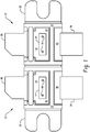
- one exemplary embodiment 10 of a package manufactured according to the method of the invention includes a dual chip package 12 with a gold-tin alloy such as AuSn, die bond sheet preforms 14 attached to die bond areas 16.
- the die bond sheet preforms 14 are secured by tack welds 18 with two spaced apart welds for each die bond sheet preform 14.
- Each die bond sheet preform 14 is solder that will be used to bond a die to the package 12 in a subsequent step.
- the illustrated package 12 (sometimes called a header) has positions for mounting two dies.
- the exemplary package or header 12 is a copper-tungsten mix which is often used in headers to provide electrical conductivity, thermal conductivity, and heat resistance.
- the package 12 has horizontal members 20 which span the width of the package 12 and are electrically connected to conductive regions 22 and 24 on the ceramic.
- Two upper leads 26 and 28 are electrically and thermally connected to conductive regions 30 and 32 on the package.
- the conductive regions 30 and 32 include the die bond regions 16.
- Two lower leads 34 and 36 are electrically and thermally connected to conductive regions 38 and 40.
- One exemplary application of the current disclosure is the mounting of gallium nitride semiconductor dies to copper tungsten packages 12. Bonding of gallium nitride to copper tungsten is better as a gold, tin mixture is used as the bonding material (i.e., a preform of gold-tin).
- the thickness of the gold-tin die bond sheet preform should be thick enough for a reliable die bond of a semiconductor die to the package 12.
- the preferred thickness is 0.0005 inch (13 ⁇ m), for example.
- the gold-tin die bond sheet preform is about the same size as the die or generally only slightly larger than the bottom of the die to be mounted thus minimizing the amount of gold used.
- the amount of gold used in accordance with the present disclosure for mounting the die on the package is less.
- the present disclosure is less time consuming and less costly. Accordingly, avoiding the plating process reduces costs.
- the process described in accordance with the present disclosure is used with headers and packages which are not gold plated.
- the use of the gold-tin sheet preform provides reliable die bonding with a minimum amount of gold.
- the preforms 14 are attached to the package 12 by tack welds 18.
- the tack welds 18 should be strong enough to keep the gold-tin die bond sheet preform 14 attached to the package 12 until a die is attached to the package.
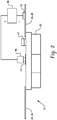
- the tack welds 18 are formed using a tack welder having welding electrodes 46 (only one is schematically shown in FIG. 2 ), an electrical power supply 48, and a work piece contact 50.
- the work piece contact 50 is pressed onto the appropriate lead 26 or 28 and the electrodes 46 are pressed onto the corresponding gold-tin die bond preform 14 at the tack weld positions 18, as shown in FIG. 2 .
- the welding electrodes 46 have working ends with a very small area of contact (e.g., 1 mm to 1.5 mm) when brought against the preform 14. This creates very small welds 18 between the preform 14 and the package 12.
- welds 18 can be very small and still hold the preform in place because two spaced apart welds are created in each preform 14. Two small, spaced welds 18 reliably hold the preform 14 in place to prevent both lateral and rotational movement of the preform 14 relative to the package 12. In one embodiment, the welds are approximately 0.3 mm to 0.5 mm.
- the gold die bond sheet preform when the die is attached, the gold die bond sheet preform must at least partially liquefy and bond to both the die and the package. Accordingly, care should be taken to minimize phase separation issues during the spot welding.
- a preheat current is applied prior to the current expected to create the weld. Applicants have found that these approaches can cause phase separation issues with a gold-tin preform.
- FIG. 3 shows the package 12 after semiconductor chips 52 and 54 have been die bonded onto the package 12.
- the chips 52 and 54 cover about 98% of the area of the die bond sheet preforms 14.
- the gold-tin die bond sheet preform shown in the drawings is rectangular, the preform will be generally shaped to the contour of the bottom of the die. Virtually any desired shape preform can be used in accordance with the present disclosure.
- FIGS. 4 and 5 show examples of packages or headers with a gold-tin preform attached.
- a gold-tin sheet is first rolled or otherwise processed to a sheet of 0.0005 inch (13 ⁇ m) thick, for example.
- the gold-tin sheet is then cut to dimensions appropriate for the die to be mounted. For instance, a die size of 20 mm x 1.2 mm might call for a preform measuring 2.1 mm x 1.3 mm.
- the thickness can remain 0.0005 inch (13 ⁇ m) for all sizes. This size preform provides adequate solder volume for this size die.
- the total amount of gold used on the package, including the gold-tin die bond sheet preform, is significantly reduced as compared to other method such as plating. Since the cost of manufacturing a custom thickness gold die bond sheet preform is much less than manufacturing a package with a custom thickness of gold plating, the cost of each of the packages for a new die type is reduced, which can become significant for small package orders by the semiconductor manufacturer.
Landscapes
- Die Bonding (AREA)
- Engineering & Computer Science (AREA)
- Manufacturing & Machinery (AREA)
- Container, Conveyance, Adherence, Positioning, Of Wafer (AREA)
Description
- This disclosure relates to the die bonding of semiconductor chips to ceramic or metals, and more particularly, to die bonding of semiconductor chips to semiconductor packages using a gold die bond sheet preform.
- Die bonding of semiconductor chips to packages or headers typically involves metalizing the semiconductor package with gold alloy and bonding of the die to the substrate. Die bonding is of critical importance for power devices, for example, that require a high quality die bond to dissipate heat from the package, and, in some cases, provide a low impedance interface between the bottom of the die and the die bond area.
- For the package manufacturer the amount of gold plated on to the semiconductor package is an important factor in the cost of the package. The thickness of the gold layer on the package must be enough to provide a secure bond surface for the die attach process. In addition, variations in die types by the same manufacturer when the die is manufactured affects die bond.
- Therefore, it can be appreciated that a package that require less gold than conventional packages while still maintaining a comparable level of performance is highly desirable.
- Further, a package in which the thickness of the gold at the die bond area can be easily adjusted to accommodate variations in die types and other features is also highly desirable.
- WIPO Patent Publication
WO 2008045779 A2 of International Application No.PCT/US2007/080552 ; applicant, Williams Advanced Materials, Inc.; Inventors Jech, David and Kothandapani, Ramesh discloses a gold-tin die bond sheet for a semiconductor package wherein the thickness of the gold plating on the package substrate is reduced and such a gold-tin die bond sheet preform is used for forming a semiconductor package. The gold-tin die preform is placed in the die bond location on the package substrate and tack welded to the package. - In accordance with the present disclosure, a method of forming a semiconductor bond site on a semiconductor package is defined according to claim 1.
- In this method, a gold-tin die bond sheet preform is used, wherein the die bond sheet preform is originally a uniform mix of gold and tin susceptible to phase separation between gold and tin by melting and resolidification.
- Yet further in accordance with the disclosure, a gold-tin die bond sheet preform may be 0.0005 inch (13 µm) thick.
- Still further in accordance with the method of claim 1, the die bond sheet preform is tack bonded by electric resistance welding to the package by means of an electric current that has a welding current waveform having only one principal current peak to minimize phase separation between gold and tin by melting and resolidification, wherein no preheat current is applied prior to the current expected to create the weld.
- The die bond sheet preform contains gold and tin. The die bond sheet preform can be 0.0005 inch (13 µm) thick. The die bond sheet preform can be rolled to a final thickness of 0.0005 inch (13 µm). The die bond sheet preform is welded to the package die bond area with an electric current resistance welding using a welding current waveform having only one principal current peak. The welding the die bond sheet preform to the package die bond area includes using a working electrode having a very small contact area (approximately 0.3 mm to 0.5 mm). The method can further include placing a die on the die bond sheet preform, and attaching the die to the package die bond area by at least partially liquefying the die bond sheet preform. The die bond sheet preform can be slightly larger than a footprint of the die. The total area of the spot welds can be approximately 0.4 mm to 0.7 mm.
- The present disclosure is described with reference to the accompanying drawings, wherein:
-
FIG. 1 is a top view of an example package ready to receive semiconductor chips or dies with a gold die bond preform manufactured according to the method of the invention; -
FIG. 2 is a combination cross section of the ceramic package ofFIG. 1 and an electrical schematic of a method of spot welding the gold die bond strip to the ceramic package; -
FIG. 3 is a top view of the ceramic package ofFIG. 1 with a semiconductor chip or die bonded to the ceramic package; -
FIG. 4 is a top view of a second example package ready to receive a semiconductor chip or die with a gold-tin preform in place; and, -
FIG. 5 is a top view of a third example package ready to receive a semiconductor chip or die with a gold-tin preform in place as manufactured according to the method of the invention. - Corresponding reference characters indicate corresponding parts throughout the several views. The elements in the drawings have not necessarily been drawn to scale in order to better illustrate the features of the disclosure. The example set out herein illustrates one embodiment of the present invention.
- Referring to
FIG. 1 , oneexemplary embodiment 10 of a package manufactured according to the method of the invention includes adual chip package 12 with a gold-tin alloy such as AuSn, diebond sheet preforms 14 attached todie bond areas 16. The diebond sheet preforms 14 are secured bytack welds 18 with two spaced apart welds for each die bond sheet preform 14. Each diebond sheet preform 14 is solder that will be used to bond a die to thepackage 12 in a subsequent step. - The illustrated package 12 (sometimes called a header) has positions for mounting two dies.
- The exemplary package or
header 12 is a copper-tungsten mix which is often used in headers to provide electrical conductivity, thermal conductivity, and heat resistance. Thepackage 12 hashorizontal members 20 which span the width of thepackage 12 and are electrically connected toconductive regions upper leads conductive regions conductive regions bond regions 16. Twolower leads conductive regions - One exemplary application of the current disclosure is the mounting of gallium nitride semiconductor dies to
copper tungsten packages 12. Bonding of gallium nitride to copper tungsten is better as a gold, tin mixture is used as the bonding material (i.e., a preform of gold-tin). - The thickness of the gold-tin die bond sheet preform should be thick enough for a reliable die bond of a semiconductor die to the
package 12. The preferred thickness is 0.0005 inch (13 µm), for example. The gold-tin die bond sheet preform is about the same size as the die or generally only slightly larger than the bottom of the die to be mounted thus minimizing the amount of gold used. - As compared to conventional techniques including gold plating applied to larger areas, the amount of gold used in accordance with the present disclosure for mounting the die on the package is less. Moreover, as compared to the plating process, the present disclosure is less time consuming and less costly. Accordingly, avoiding the plating process reduces costs. The process described in accordance with the present disclosure is used with headers and packages which are not gold plated. The use of the gold-tin sheet preform provides reliable die bonding with a minimum amount of gold.
- Turning now to
FIG. 2 , thepreforms 14 are attached to thepackage 12 bytack welds 18. It will be appreciated that thetack welds 18 should be strong enough to keep the gold-tin diebond sheet preform 14 attached to thepackage 12 until a die is attached to the package. Thetack welds 18 are formed using a tack welder having welding electrodes 46 (only one is schematically shown inFIG. 2 ), anelectrical power supply 48, and awork piece contact 50. Thework piece contact 50 is pressed onto theappropriate lead electrodes 46 are pressed onto the corresponding gold-tin die bond preform 14 at thetack weld positions 18, as shown inFIG. 2 . Thewelding electrodes 46 have working ends with a very small area of contact (e.g., 1 mm to 1.5 mm) when brought against thepreform 14. This creates verysmall welds 18 between thepreform 14 and thepackage 12. - Applicants have found that the
welds 18 can be very small and still hold the preform in place because two spaced apart welds are created in eachpreform 14. Two small,spaced welds 18 reliably hold thepreform 14 in place to prevent both lateral and rotational movement of thepreform 14 relative to thepackage 12. In one embodiment, the welds are approximately 0.3 mm to 0.5 mm. - The gold-tin sheet for use in accordance with the present disclosure is originally a uniform mix of gold and tin. Gold-tin foil or sheet can be changed by melting and resolidification. For example, the gold and tin can separate in what is sometimes called phase separation. If this occurs to a large portion of the gold-tin sheet used to bond a die to a package, the bond may be compromised to the point of unreliability.
- It will be appreciated that when the die is attached, the gold die bond sheet preform must at least partially liquefy and bond to both the die and the package. Accordingly, care should be taken to minimize phase separation issues during the spot welding.
- In accordance with the present disclosure, phase separation issues are minimized by i) creating only very small weld areas (areas of melting), and ii) by applying welding current to the electrodes with a single principal current peak. Dual pulse resistance welding is performed to bond the gold-tin preforms onto the package.
- In some spot welding approaches, a preheat current is applied prior to the current expected to create the weld. Applicants have found that these approaches can cause phase separation issues with a gold-tin preform.
- In accordance with the present disclosure applicants concentrate current in one peak during the spot welding process to avoid phase separation issues that occur in other spot welding approaches.
-
FIG. 3 shows thepackage 12 after semiconductor chips 52 and 54 have been die bonded onto thepackage 12. In one particular embodiment thechips - While the gold-tin die bond sheet preform shown in the drawings is rectangular, the preform will be generally shaped to the contour of the bottom of the die. Virtually any desired shape preform can be used in accordance with the present disclosure.
-
FIGS. 4 and 5 show examples of packages or headers with a gold-tin preform attached. A gold-tin sheet is first rolled or otherwise processed to a sheet of 0.0005 inch (13 µm) thick, for example. The gold-tin sheet is then cut to dimensions appropriate for the die to be mounted. For instance, a die size of 20 mm x 1.2 mm might call for a preform measuring 2.1 mm x 1.3 mm. The thickness can remain 0.0005 inch (13 µm) for all sizes. This size preform provides adequate solder volume for this size die. - It will be appreciated that the
preforms 14 should be placed with precision in the location where the die is to be mounted to thepackage 12 so the solder (gold-tin) is where it can be used in bonding. Accordingly, very tight tolerances are used in preform attachment. This becomes very important when the die is placed for attachment. Often the die is placed on the package or header without pressure applied. If the preform on which the die is placed is not anchored, the die may move. In the illustrated embodiments, the preform is held in place by the tack welds such that the die does not move and is mounted at its intended location. - As described above, since the entire package does not have to have enough gold plating for reliably die bonding a chip to the package, the total amount of gold used on the package, including the gold-tin die bond sheet preform, is significantly reduced as compared to other method such as plating. Since the cost of manufacturing a custom thickness gold die bond sheet preform is much less than manufacturing a package with a custom thickness of gold plating, the cost of each of the packages for a new die type is reduced, which can become significant for small package orders by the semiconductor manufacturer.
- While the disclosure has been described with reference to particular embodiments, it will be understood by those skilled in the art that the invention is not limited to these embodiments, the scope being defined by the appended claims.
Claims (5)
- A method of forming a semiconductor bond site on a semiconductor package (12) comprising a copper-tungsten base, comprising the steps of:forming a die bond sheet preform (14) containing gold and tin having a width, a length and a uniform thickness;placing the die bond sheet preform (14) on a die bond area (16) on the semiconductor package (12); andwelding the die bond sheet preform (14) to the package die bond area (16) at two spaced apart spots (18), the two spaced apart spots (18) having a total area significantly smaller than the area of the sheet preform (14),characterized in thatthe semiconductor package (12) is not gold plated;the die bond sheet preform (14) is originally a uniform mix of gold and tin susceptible to phase separation between gold and tin by melting and resolidification; andthe die bond sheet preform (14) is welded to the package die bond area (16) with an electric current resistance welding using a welding current waveform having only one principal current peak to minimize said phase separation, wherein no preheat current is applied prior to the current expected to create the weld.
- The method of claim 1, wherein the die bond sheet preform (14) is 13 µm (0.0005 inch) thick.
- The method of claim 1 or 2, wherein the die bond sheet preform (14) is rolled to a final thickness.
- The method of any one of claims 1 to 3 further comprising placing a die (52, 54) on the die bond sheet preform (14).
- The method of claim 4 further comprising attaching the die (52, 54) to the package die bond area (16) by at least partially liquefying the die bond sheet preform (14).
Applications Claiming Priority (2)
| Application Number | Priority Date | Filing Date | Title |
|---|---|---|---|
| US201361793751P | 2013-03-15 | 2013-03-15 | |
| PCT/US2014/023872 WO2014150643A1 (en) | 2013-03-15 | 2014-03-12 | Gold containing die bond sheet preform spot-welded to a semiconductor bond site on a semiconductor package and corresponding manufacturing method |
Publications (2)
| Publication Number | Publication Date |
|---|---|
| EP2973672A1 EP2973672A1 (en) | 2016-01-20 |
| EP2973672B1 true EP2973672B1 (en) | 2018-07-11 |
Family
ID=50686120
Family Applications (1)
| Application Number | Title | Priority Date | Filing Date |
|---|---|---|---|
| EP14722830.8A Active EP2973672B1 (en) | 2013-03-15 | 2014-03-12 | Method of spot-welding a die bond sheet preform containing gold and tin to a die bond area on a semiconductor package |
Country Status (7)
| Country | Link |
|---|---|
| US (1) | US8975176B2 (en) |
| EP (1) | EP2973672B1 (en) |
| CN (1) | CN105122436B (en) |
| MY (1) | MY172913A (en) |
| PH (1) | PH12015502124B1 (en) |
| SG (1) | SG11201507552WA (en) |
| WO (1) | WO2014150643A1 (en) |
Families Citing this family (3)
| Publication number | Priority date | Publication date | Assignee | Title |
|---|---|---|---|---|
| US10211115B2 (en) | 2014-05-21 | 2019-02-19 | Materion Corporation | Method of making a ceramic combo lid with selective and edge metallizations |
| WO2016053390A1 (en) | 2014-10-01 | 2016-04-07 | Materion Corporation | Cover lid with selective and edge metallization |
| WO2022235914A1 (en) | 2021-05-07 | 2022-11-10 | Materion Corporation | Microelectronics package assemblies and processes for making |
Citations (1)
| Publication number | Priority date | Publication date | Assignee | Title |
|---|---|---|---|---|
| WO1991009699A1 (en) * | 1989-12-29 | 1991-07-11 | Williams Advanced Materials Inc. | Welding of solder frame to ceramic lid in semi-conductor packaging |
Family Cites Families (25)
| Publication number | Priority date | Publication date | Assignee | Title |
|---|---|---|---|---|
| GB1047390A (en) * | 1963-05-20 | 1900-01-01 | ||
| US3495322A (en) | 1967-07-20 | 1970-02-17 | Motorola Inc | Process for bonding a silicon wafer to a ceramic substrate |
| JPS553815B1 (en) | 1967-10-02 | 1980-01-26 | ||
| US3660632A (en) | 1970-06-17 | 1972-05-02 | Us Navy | Method for bonding silicon chips to a cold substrate |
| US3728090A (en) | 1970-06-30 | 1973-04-17 | Texas Instruments Inc | Semiconductor bonding alloy |
| US4181249A (en) * | 1977-08-26 | 1980-01-01 | Hughes Aircraft Company | Eutectic die attachment method for integrated circuits |
| US4620215A (en) * | 1982-04-16 | 1986-10-28 | Amdahl Corporation | Integrated circuit packaging systems with double surface heat dissipation |
| US4650922A (en) * | 1985-03-11 | 1987-03-17 | Texas Instruments Incorporated | Thermally matched mounting substrate |
| US4872047A (en) | 1986-11-07 | 1989-10-03 | Olin Corporation | Semiconductor die attach system |
| US5037778A (en) | 1989-05-12 | 1991-08-06 | Intel Corporation | Die attach using gold ribbon with gold/silicon eutectic alloy cladding |
| JP3181283B2 (en) | 1989-08-07 | 2001-07-03 | 株式会社日立製作所 | Solder-connected electronic circuit device, solder connection method, and solder for gold-plated connection terminals |
| JP2946837B2 (en) * | 1991-05-16 | 1999-09-06 | ミツミ電機株式会社 | Manufacturing method of preform for die bonding |
| JP2994510B2 (en) * | 1992-02-10 | 1999-12-27 | ローム株式会社 | Semiconductor device and manufacturing method thereof |
| JPH05226564A (en) * | 1992-02-14 | 1993-09-03 | Rohm Co Ltd | Semiconductor device |
| US5667884A (en) | 1993-04-12 | 1997-09-16 | Bolger; Justin C. | Area bonding conductive adhesive preforms |
| US5666004A (en) * | 1994-09-28 | 1997-09-09 | Intel Corporation | Use of tantalum oxide capacitor on ceramic co-fired technology |
| US5622305A (en) | 1995-05-10 | 1997-04-22 | Lucent Technologies Inc. | Bonding scheme using group VB metallic layer |
| KR100522223B1 (en) | 1997-01-24 | 2005-12-21 | 로무 가부시키가이샤 | Semiconductor device and method for manufacturing thereof |
| US5930666A (en) | 1997-10-09 | 1999-07-27 | Astralux, Incorporated | Method and apparatus for packaging high temperature solid state electronic devices |
| US20050136640A1 (en) | 2002-01-07 | 2005-06-23 | Chuan Hu | Die exhibiting an effective coefficient of thermal expansion equivalent to a substrate mounted thereon, and processes of making same |
| CN101218678A (en) * | 2005-05-04 | 2008-07-09 | Nxp股份有限公司 | Device comprising a sensor module |
| US20090052386A1 (en) | 2006-07-04 | 2009-02-26 | Masaaki Higashida | Radio communication system |
| WO2008045779A2 (en) * | 2006-10-06 | 2008-04-17 | Williams Advanced Materials, Inc. | Gold die bond sheet preform |
| US7595553B2 (en) | 2006-11-08 | 2009-09-29 | Sanyo Electric Co., Ltd. | Packaging board and manufacturing method therefor, semiconductor module and mobile apparatus |
| US8212277B2 (en) | 2008-07-29 | 2012-07-03 | Stanley Electric Co., Ltd. | Optical semiconductor device module with power supply through uneven contacts |
-
2014
- 2014-03-12 SG SG11201507552WA patent/SG11201507552WA/en unknown
- 2014-03-12 US US14/205,403 patent/US8975176B2/en active Active
- 2014-03-12 EP EP14722830.8A patent/EP2973672B1/en active Active
- 2014-03-12 CN CN201480022044.2A patent/CN105122436B/en active Active
- 2014-03-12 WO PCT/US2014/023872 patent/WO2014150643A1/en not_active Ceased
- 2014-03-12 MY MYPI2015703149A patent/MY172913A/en unknown
-
2015
- 2015-09-14 PH PH12015502124A patent/PH12015502124B1/en unknown
Patent Citations (1)
| Publication number | Priority date | Publication date | Assignee | Title |
|---|---|---|---|---|
| WO1991009699A1 (en) * | 1989-12-29 | 1991-07-11 | Williams Advanced Materials Inc. | Welding of solder frame to ceramic lid in semi-conductor packaging |
Non-Patent Citations (1)
| Title |
|---|
| -: "Dual Pulse Resistance Welders CD125DP/CD250DP/CD375DP. Professional Capacitive Discharge Spot Welding Systems", 10 November 2006 (2006-11-10), XP055427687, Retrieved from the Internet <URL:https://web.archive.org/web/20061110003448/http://www.spotweldingconsultants.com/sunstone/pdf/SunstoneDPWelderDS.pdf> [retrieved on 20171122] * |
Also Published As
| Publication number | Publication date |
|---|---|
| US20140264949A1 (en) | 2014-09-18 |
| MY172913A (en) | 2019-12-13 |
| EP2973672A1 (en) | 2016-01-20 |
| PH12015502124A1 (en) | 2016-01-25 |
| PH12015502124B1 (en) | 2016-01-25 |
| CN105122436A (en) | 2015-12-02 |
| WO2014150643A1 (en) | 2014-09-25 |
| SG11201507552WA (en) | 2015-10-29 |
| CN105122436B (en) | 2018-09-25 |
| US8975176B2 (en) | 2015-03-10 |
Similar Documents
| Publication | Publication Date | Title |
|---|---|---|
| US10147671B2 (en) | Semiconductor device and method for manufacturing same | |
| CN202454546U (en) | Semiconductor device | |
| US8975117B2 (en) | Semiconductor device using diffusion soldering | |
| CN107210289B (en) | Semiconductor device | |
| CN113808953B (en) | Batch welding of different components in power modules | |
| EP4145495A1 (en) | Method of manufacturing an electrical interconnect for a semiconductor device as well as the corresponding device having the same | |
| US20160365305A1 (en) | Lead frame with conductive clip for mounting a semiconductor die with reduced clip shifting | |
| SE512906C2 (en) | Procedure for soldering a semiconductor chip and RF power transistor for conducting it | |
| US8975176B2 (en) | Gold die bond sheet preform | |
| EP2768015A1 (en) | Gold/silicon eutectic chip soldering method and transistor | |
| JP2015144169A (en) | semiconductor module | |
| US6601752B2 (en) | Electronic part mounting method | |
| JP6619121B1 (en) | Semiconductor device manufacturing method, semiconductor device manufacturing jig, and semiconductor device | |
| US10879211B2 (en) | Method of joining a surface-mount component to a substrate with solder that has been temporarily secured | |
| US20170323801A1 (en) | Method of generating a power semiconductor module | |
| US20230040019A1 (en) | Semiconductor device and method of manufacturing the same | |
| US20250372496A1 (en) | Semiconductor device and method for manufacturing semiconductor device | |
| JP2012222316A (en) | Thermal compression bonding heater chip, and thermal compression bonding method | |
| WO2008045779A2 (en) | Gold die bond sheet preform | |
| JP6344605B2 (en) | Manufacturing method of semiconductor device | |
| WO2016182425A1 (en) | A lead frame for selective soldering | |
| JP2007123647A (en) | Heater chip thermocouple mounting structure and thermocouple mounting method | |
| CN104900602A (en) | Power module and method for controlling thickness of solder in power module manufacturing process | |
| CN119993917A (en) | Semiconductor device and method for manufacturing the same | |
| JP2006295074A (en) | Manufacturing method of package for semiconductor device |
Legal Events
| Date | Code | Title | Description |
|---|---|---|---|
| PUAI | Public reference made under article 153(3) epc to a published international application that has entered the european phase |
Free format text: ORIGINAL CODE: 0009012 |
|
| 17P | Request for examination filed |
Effective date: 20151014 |
|
| AK | Designated contracting states |
Kind code of ref document: A1 Designated state(s): AL AT BE BG CH CY CZ DE DK EE ES FI FR GB GR HR HU IE IS IT LI LT LU LV MC MK MT NL NO PL PT RO RS SE SI SK SM TR |
|
| AX | Request for extension of the european patent |
Extension state: BA ME |
|
| DAX | Request for extension of the european patent (deleted) | ||
| 17Q | First examination report despatched |
Effective date: 20160919 |
|
| STAA | Information on the status of an ep patent application or granted ep patent |
Free format text: STATUS: EXAMINATION IS IN PROGRESS |
|
| RIC1 | Information provided on ipc code assigned before grant |
Ipc: H01L 23/488 20060101ALN20171221BHEP Ipc: H01L 21/60 20060101AFI20171221BHEP |
|
| GRAP | Despatch of communication of intention to grant a patent |
Free format text: ORIGINAL CODE: EPIDOSNIGR1 |
|
| STAA | Information on the status of an ep patent application or granted ep patent |
Free format text: STATUS: GRANT OF PATENT IS INTENDED |
|
| INTG | Intention to grant announced |
Effective date: 20180201 |
|
| GRAS | Grant fee paid |
Free format text: ORIGINAL CODE: EPIDOSNIGR3 |
|
| GRAA | (expected) grant |
Free format text: ORIGINAL CODE: 0009210 |
|
| STAA | Information on the status of an ep patent application or granted ep patent |
Free format text: STATUS: THE PATENT HAS BEEN GRANTED |
|
| AK | Designated contracting states |
Kind code of ref document: B1 Designated state(s): AL AT BE BG CH CY CZ DE DK EE ES FI FR GB GR HR HU IE IS IT LI LT LU LV MC MK MT NL NO PL PT RO RS SE SI SK SM TR |
|
| REG | Reference to a national code |
Ref country code: GB Ref legal event code: FG4D |
|
| REG | Reference to a national code |
Ref country code: CH Ref legal event code: EP |
|
| REG | Reference to a national code |
Ref country code: AT Ref legal event code: REF Ref document number: 1017794 Country of ref document: AT Kind code of ref document: T Effective date: 20180715 |
|
| REG | Reference to a national code |
Ref country code: IE Ref legal event code: FG4D |
|
| REG | Reference to a national code |
Ref country code: DE Ref legal event code: R096 Ref document number: 602014028262 Country of ref document: DE |
|
| REG | Reference to a national code |
Ref country code: NL Ref legal event code: FP |
|
| REG | Reference to a national code |
Ref country code: LT Ref legal event code: MG4D |
|
| REG | Reference to a national code |
Ref country code: AT Ref legal event code: MK05 Ref document number: 1017794 Country of ref document: AT Kind code of ref document: T Effective date: 20180711 |
|
| PG25 | Lapsed in a contracting state [announced via postgrant information from national office to epo] |
Ref country code: NO Free format text: LAPSE BECAUSE OF FAILURE TO SUBMIT A TRANSLATION OF THE DESCRIPTION OR TO PAY THE FEE WITHIN THE PRESCRIBED TIME-LIMIT Effective date: 20181011 Ref country code: GR Free format text: LAPSE BECAUSE OF FAILURE TO SUBMIT A TRANSLATION OF THE DESCRIPTION OR TO PAY THE FEE WITHIN THE PRESCRIBED TIME-LIMIT Effective date: 20181012 Ref country code: BG Free format text: LAPSE BECAUSE OF FAILURE TO SUBMIT A TRANSLATION OF THE DESCRIPTION OR TO PAY THE FEE WITHIN THE PRESCRIBED TIME-LIMIT Effective date: 20181011 Ref country code: SE Free format text: LAPSE BECAUSE OF FAILURE TO SUBMIT A TRANSLATION OF THE DESCRIPTION OR TO PAY THE FEE WITHIN THE PRESCRIBED TIME-LIMIT Effective date: 20180711 Ref country code: IS Free format text: LAPSE BECAUSE OF FAILURE TO SUBMIT A TRANSLATION OF THE DESCRIPTION OR TO PAY THE FEE WITHIN THE PRESCRIBED TIME-LIMIT Effective date: 20181111 Ref country code: AT Free format text: LAPSE BECAUSE OF FAILURE TO SUBMIT A TRANSLATION OF THE DESCRIPTION OR TO PAY THE FEE WITHIN THE PRESCRIBED TIME-LIMIT Effective date: 20180711 Ref country code: LT Free format text: LAPSE BECAUSE OF FAILURE TO SUBMIT A TRANSLATION OF THE DESCRIPTION OR TO PAY THE FEE WITHIN THE PRESCRIBED TIME-LIMIT Effective date: 20180711 Ref country code: PL Free format text: LAPSE BECAUSE OF FAILURE TO SUBMIT A TRANSLATION OF THE DESCRIPTION OR TO PAY THE FEE WITHIN THE PRESCRIBED TIME-LIMIT Effective date: 20180711 Ref country code: RS Free format text: LAPSE BECAUSE OF FAILURE TO SUBMIT A TRANSLATION OF THE DESCRIPTION OR TO PAY THE FEE WITHIN THE PRESCRIBED TIME-LIMIT Effective date: 20180711 Ref country code: FI Free format text: LAPSE BECAUSE OF FAILURE TO SUBMIT A TRANSLATION OF THE DESCRIPTION OR TO PAY THE FEE WITHIN THE PRESCRIBED TIME-LIMIT Effective date: 20180711 |
|
| PG25 | Lapsed in a contracting state [announced via postgrant information from national office to epo] |
Ref country code: ES Free format text: LAPSE BECAUSE OF FAILURE TO SUBMIT A TRANSLATION OF THE DESCRIPTION OR TO PAY THE FEE WITHIN THE PRESCRIBED TIME-LIMIT Effective date: 20180711 Ref country code: HR Free format text: LAPSE BECAUSE OF FAILURE TO SUBMIT A TRANSLATION OF THE DESCRIPTION OR TO PAY THE FEE WITHIN THE PRESCRIBED TIME-LIMIT Effective date: 20180711 Ref country code: AL Free format text: LAPSE BECAUSE OF FAILURE TO SUBMIT A TRANSLATION OF THE DESCRIPTION OR TO PAY THE FEE WITHIN THE PRESCRIBED TIME-LIMIT Effective date: 20180711 Ref country code: LV Free format text: LAPSE BECAUSE OF FAILURE TO SUBMIT A TRANSLATION OF THE DESCRIPTION OR TO PAY THE FEE WITHIN THE PRESCRIBED TIME-LIMIT Effective date: 20180711 |
|
| REG | Reference to a national code |
Ref country code: DE Ref legal event code: R097 Ref document number: 602014028262 Country of ref document: DE |
|
| PG25 | Lapsed in a contracting state [announced via postgrant information from national office to epo] |
Ref country code: EE Free format text: LAPSE BECAUSE OF FAILURE TO SUBMIT A TRANSLATION OF THE DESCRIPTION OR TO PAY THE FEE WITHIN THE PRESCRIBED TIME-LIMIT Effective date: 20180711 Ref country code: IT Free format text: LAPSE BECAUSE OF FAILURE TO SUBMIT A TRANSLATION OF THE DESCRIPTION OR TO PAY THE FEE WITHIN THE PRESCRIBED TIME-LIMIT Effective date: 20180711 Ref country code: CZ Free format text: LAPSE BECAUSE OF FAILURE TO SUBMIT A TRANSLATION OF THE DESCRIPTION OR TO PAY THE FEE WITHIN THE PRESCRIBED TIME-LIMIT Effective date: 20180711 Ref country code: RO Free format text: LAPSE BECAUSE OF FAILURE TO SUBMIT A TRANSLATION OF THE DESCRIPTION OR TO PAY THE FEE WITHIN THE PRESCRIBED TIME-LIMIT Effective date: 20180711 |
|
| PLBE | No opposition filed within time limit |
Free format text: ORIGINAL CODE: 0009261 |
|
| STAA | Information on the status of an ep patent application or granted ep patent |
Free format text: STATUS: NO OPPOSITION FILED WITHIN TIME LIMIT |
|
| PG25 | Lapsed in a contracting state [announced via postgrant information from national office to epo] |
Ref country code: SK Free format text: LAPSE BECAUSE OF FAILURE TO SUBMIT A TRANSLATION OF THE DESCRIPTION OR TO PAY THE FEE WITHIN THE PRESCRIBED TIME-LIMIT Effective date: 20180711 Ref country code: DK Free format text: LAPSE BECAUSE OF FAILURE TO SUBMIT A TRANSLATION OF THE DESCRIPTION OR TO PAY THE FEE WITHIN THE PRESCRIBED TIME-LIMIT Effective date: 20180711 Ref country code: SM Free format text: LAPSE BECAUSE OF FAILURE TO SUBMIT A TRANSLATION OF THE DESCRIPTION OR TO PAY THE FEE WITHIN THE PRESCRIBED TIME-LIMIT Effective date: 20180711 |
|
| 26N | No opposition filed |
Effective date: 20190412 |
|
| PG25 | Lapsed in a contracting state [announced via postgrant information from national office to epo] |
Ref country code: SI Free format text: LAPSE BECAUSE OF FAILURE TO SUBMIT A TRANSLATION OF THE DESCRIPTION OR TO PAY THE FEE WITHIN THE PRESCRIBED TIME-LIMIT Effective date: 20180711 |
|
| PG25 | Lapsed in a contracting state [announced via postgrant information from national office to epo] |
Ref country code: MC Free format text: LAPSE BECAUSE OF FAILURE TO SUBMIT A TRANSLATION OF THE DESCRIPTION OR TO PAY THE FEE WITHIN THE PRESCRIBED TIME-LIMIT Effective date: 20180711 |
|
| REG | Reference to a national code |
Ref country code: CH Ref legal event code: PL |
|
| PG25 | Lapsed in a contracting state [announced via postgrant information from national office to epo] |
Ref country code: LU Free format text: LAPSE BECAUSE OF NON-PAYMENT OF DUE FEES Effective date: 20190312 |
|
| PG25 | Lapsed in a contracting state [announced via postgrant information from national office to epo] |
Ref country code: IE Free format text: LAPSE BECAUSE OF NON-PAYMENT OF DUE FEES Effective date: 20190312 Ref country code: CH Free format text: LAPSE BECAUSE OF NON-PAYMENT OF DUE FEES Effective date: 20190331 Ref country code: LI Free format text: LAPSE BECAUSE OF NON-PAYMENT OF DUE FEES Effective date: 20190331 |
|
| PG25 | Lapsed in a contracting state [announced via postgrant information from national office to epo] |
Ref country code: TR Free format text: LAPSE BECAUSE OF FAILURE TO SUBMIT A TRANSLATION OF THE DESCRIPTION OR TO PAY THE FEE WITHIN THE PRESCRIBED TIME-LIMIT Effective date: 20180711 |
|
| PG25 | Lapsed in a contracting state [announced via postgrant information from national office to epo] |
Ref country code: MT Free format text: LAPSE BECAUSE OF NON-PAYMENT OF DUE FEES Effective date: 20190312 Ref country code: PT Free format text: LAPSE BECAUSE OF FAILURE TO SUBMIT A TRANSLATION OF THE DESCRIPTION OR TO PAY THE FEE WITHIN THE PRESCRIBED TIME-LIMIT Effective date: 20181111 |
|
| PG25 | Lapsed in a contracting state [announced via postgrant information from national office to epo] |
Ref country code: CY Free format text: LAPSE BECAUSE OF FAILURE TO SUBMIT A TRANSLATION OF THE DESCRIPTION OR TO PAY THE FEE WITHIN THE PRESCRIBED TIME-LIMIT Effective date: 20180711 |
|
| PG25 | Lapsed in a contracting state [announced via postgrant information from national office to epo] |
Ref country code: HU Free format text: LAPSE BECAUSE OF FAILURE TO SUBMIT A TRANSLATION OF THE DESCRIPTION OR TO PAY THE FEE WITHIN THE PRESCRIBED TIME-LIMIT; INVALID AB INITIO Effective date: 20140312 |
|
| PG25 | Lapsed in a contracting state [announced via postgrant information from national office to epo] |
Ref country code: MK Free format text: LAPSE BECAUSE OF FAILURE TO SUBMIT A TRANSLATION OF THE DESCRIPTION OR TO PAY THE FEE WITHIN THE PRESCRIBED TIME-LIMIT Effective date: 20180711 |
|
| P01 | Opt-out of the competence of the unified patent court (upc) registered |
Effective date: 20230515 |
|
| REG | Reference to a national code |
Ref country code: DE Ref legal event code: R079 Ref document number: 602014028262 Country of ref document: DE Free format text: PREVIOUS MAIN CLASS: H01L0021600000 Ipc: H10W0070010000 |
|
| PGFP | Annual fee paid to national office [announced via postgrant information from national office to epo] |
Ref country code: NL Payment date: 20260227 Year of fee payment: 13 |
|
| PGFP | Annual fee paid to national office [announced via postgrant information from national office to epo] |
Ref country code: GB Payment date: 20260303 Year of fee payment: 13 |
|
| PGFP | Annual fee paid to national office [announced via postgrant information from national office to epo] |
Ref country code: DE Payment date: 20260225 Year of fee payment: 13 |
|
| PGFP | Annual fee paid to national office [announced via postgrant information from national office to epo] |
Ref country code: BE Payment date: 20260227 Year of fee payment: 13 |
|
| PGFP | Annual fee paid to national office [announced via postgrant information from national office to epo] |
Ref country code: FR Payment date: 20260223 Year of fee payment: 13 |