EP2966507A1 - Image forming apparatus for determining defects of light-emitting element array chips - Google Patents
Image forming apparatus for determining defects of light-emitting element array chips Download PDFInfo
- Publication number
- EP2966507A1 EP2966507A1 EP15168497.4A EP15168497A EP2966507A1 EP 2966507 A1 EP2966507 A1 EP 2966507A1 EP 15168497 A EP15168497 A EP 15168497A EP 2966507 A1 EP2966507 A1 EP 2966507A1
- Authority
- EP
- European Patent Office
- Prior art keywords
- light
- emitting element
- element array
- image forming
- forming apparatus
- Prior art date
- Legal status (The legal status is an assumption and is not a legal conclusion. Google has not performed a legal analysis and makes no representation as to the accuracy of the status listed.)
- Granted
Links
Images













Classifications
-
- B—PERFORMING OPERATIONS; TRANSPORTING
- B41—PRINTING; LINING MACHINES; TYPEWRITERS; STAMPS
- B41J—TYPEWRITERS; SELECTIVE PRINTING MECHANISMS, i.e. MECHANISMS PRINTING OTHERWISE THAN FROM A FORME; CORRECTION OF TYPOGRAPHICAL ERRORS
- B41J2/00—Typewriters or selective printing mechanisms characterised by the printing or marking process for which they are designed
- B41J2/435—Typewriters or selective printing mechanisms characterised by the printing or marking process for which they are designed characterised by selective application of radiation to a printing material or impression-transfer material
- B41J2/447—Typewriters or selective printing mechanisms characterised by the printing or marking process for which they are designed characterised by selective application of radiation to a printing material or impression-transfer material using arrays of radiation sources
- B41J2/45—Typewriters or selective printing mechanisms characterised by the printing or marking process for which they are designed characterised by selective application of radiation to a printing material or impression-transfer material using arrays of radiation sources using light-emitting diode [LED] or laser arrays
-
- G—PHYSICS
- G01—MEASURING; TESTING
- G01R—MEASURING ELECTRIC VARIABLES; MEASURING MAGNETIC VARIABLES
- G01R31/00—Arrangements for testing electric properties; Arrangements for locating electric faults; Arrangements for electrical testing characterised by what is being tested not provided for elsewhere
- G01R31/44—Testing lamps
-
- G—PHYSICS
- G03—PHOTOGRAPHY; CINEMATOGRAPHY; ANALOGOUS TECHNIQUES USING WAVES OTHER THAN OPTICAL WAVES; ELECTROGRAPHY; HOLOGRAPHY
- G03G—ELECTROGRAPHY; ELECTROPHOTOGRAPHY; MAGNETOGRAPHY
- G03G15/00—Apparatus for electrographic processes using a charge pattern
- G03G15/04—Apparatus for electrographic processes using a charge pattern for exposing, i.e. imagewise exposure by optically projecting the original image on a photoconductive recording material
- G03G15/04036—Details of illuminating systems, e.g. lamps, reflectors
- G03G15/04045—Details of illuminating systems, e.g. lamps, reflectors for exposing image information provided otherwise than by directly projecting the original image onto the photoconductive recording material, e.g. digital copiers
- G03G15/04054—Details of illuminating systems, e.g. lamps, reflectors for exposing image information provided otherwise than by directly projecting the original image onto the photoconductive recording material, e.g. digital copiers by LED arrays
-
- H—ELECTRICITY
- H04—ELECTRIC COMMUNICATION TECHNIQUE
- H04N—PICTORIAL COMMUNICATION, e.g. TELEVISION
- H04N1/00—Scanning, transmission or reproduction of documents or the like, e.g. facsimile transmission; Details thereof
- H04N1/024—Details of scanning heads ; Means for illuminating the original
- H04N1/032—Details of scanning heads ; Means for illuminating the original for picture information reproduction
-
- H—ELECTRICITY
- H04—ELECTRIC COMMUNICATION TECHNIQUE
- H04N—PICTORIAL COMMUNICATION, e.g. TELEVISION
- H04N1/00—Scanning, transmission or reproduction of documents or the like, e.g. facsimile transmission; Details thereof
- H04N1/024—Details of scanning heads ; Means for illuminating the original
- H04N1/032—Details of scanning heads ; Means for illuminating the original for picture information reproduction
- H04N1/036—Details of scanning heads ; Means for illuminating the original for picture information reproduction for optical reproduction
Definitions
- the present invention relates to an image forming apparatus, particularly to an image forming apparatus capable of determining whether any of light-emitting element array chips are defective.
- An image forming apparatus using light-emitting element array chips receives print data from a personal computer (PC) and forms an image by using light-emitting elements.
- PC personal computer
- an electrostatic latent image is formed on a photoconductor drum in the image forming apparatus. Thereafter, a print image is output through development, transfer, and fusing processes.
- a light-emitting element array chip included among the light-emitting element array chips may be defective. Light-emitting elements of a defective light-emitting element array chip may not emit light, thus causing an error. That is, printing data not being printed on paper.
- One or more exemplary embodiments include an image forming apparatus capable of determining whether any of light-emitting element array chips are defective.
- an image forming apparatus includes a plurality of light-emitting element array chips including a light-emitting element array and a transfer element array; and a control driver applying a signal to the plurality of light-emitting element array chips.
- the control driver includes a check terminal that measures signals output from the plurality of light-emitting element array chips, and the control driver determines whether any of the plurality of light-emitting element array chips are defective by analyzing the signals measured at the check terminal.
- an image forming apparatus includes a plurality light-emitting element array chips including a light-emitting element array and a transfer element array, and a control driver applying a signal to the light-emitting element array chips.
- Light-emitting element arrays included in the plurality of light-emitting element array chips are connected in parallel, and the control driver determines whether any of the light-emitting element arrays are defective by analyzing signals output from the light-emitting element arrays that are connected in parallel.
- an image forming apparatus may perform operations for outputting an image.
- the image forming apparatus may form an electrostatic latent image on a photoconductor drum 300 by using light-emitting elements and output an image through development, transfer, and fusing processes including electrification 1, exposure 2, development 3, transfer 4, fusing 5.
- the image forming apparatus may include a control driver 110, a chip array 120, a lens array 200, and the photoconductor drum 300.
- the control driver 110 may control the chip array 120 according to the print data received from the PC 50.
- the chip array 120 may include a plurality of light-emitting element array chips.
- the control driver 110 may separately control the light-emitting element array chips.
- the lens array 200 may be arranged in an axial direction (i.e., a main scanning direction) of the photoconductor drum 300. Light having passed through the lens array 200 may form an image on a surface of the photoconductor drum 300.
- the photoconductor drum 300 may be exposed to light to form an electrostatic latent image.
- a developer (not shown) may develop the electrostatic latent image formed on the photoconductor drum 300.
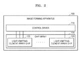
- FIG. 2 is a diagram illustrating an image forming apparatus 100 according to an exemplary embodiment.
- the image forming apparatus 100 includes a control driver 110 and a plurality of light-emitting element array chips 125.
- the control driver 110 determines whether any of the light-emitting element array chips 125 are defective. The control driver 110 determines whether any of the light-emitting element array chips 125 are defective, determines which of the light-emitting element array chips 125 are defective, and determines which light-emitting elements or which transfer elements are defective in the light-emitting element array chips 125.
- the control driver 110 includes a check terminal that measures signals output from the light-emitting element array chips 125, analyzes the signals measured at the check terminal, and determines whether any of the light-emitting element array chips 125 are defective. A method of determining whether any of the light-emitting element array chips 125 are defective, which may be performed by the control driver 110, will be described in detail below.
- the control driver 110 includes a terminal that outputs signals and a terminal that receives signals.
- the control driver 110 includes a terminal that outputs signals for controlling a transfer element or a light-emitting element and a terminal that receives signals from the transfer element or the light-emitting element.
- the control driver 110 may include at least one check terminal for determining whether any of the light-emitting element array chips 125 are defective.
- the control driver 110 receives print data and operates according to the received print data.
- the control driver 110 receives the print data from a main board or a central processing unit (CPU) included in the image forming apparatus 100, and controls on/off of the light-emitting elements according to the received print data.
- the print data is data representing an image to be formed.
- the control driver 110 may be software that is executed by at least one processor. Alternatively, the control driver 110 may be hardware such as a control driver.
- Each of the light-emitting element array chips 125 includes a transfer element array and a light-emitting element array.
- the transfer element array includes include a plurality of transfer elements, and the light-emitting element array includes a plurality of light-emitting elements.
- the transfer elements may sequentially turn the light-emitting elements on and off.
- the transfer elements and the light-emitting elements may be one-to-one matched.
- Light emission conditions of the light-emitting elements may be determined according to states of the transfer elements. In order for a light-emitting element to emit light, a transfer element corresponding to the light-emitting element has to be in a standby state.
- the on/off of the light-emitting element may be determined according to a data signal input to the light-emitting element.
- the transfer elements may sequentially enter a standby signal according to a transfer signal.
- the light-emitting element array chips 125 receive signals from the control driver 110 and operate according to the received signals.
- the light-emitting element array chips 125 may be separately controlled by the control driver 110.
- the light-emitting element array chips 125 may be connected in parallel. Data lines of the light-emitting element array chips 125 may be connected in parallel, and gates of last transfer elements of the transfer element arrays may be connected in parallel.
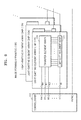
- FIG. 3 is a diagram illustrating the image forming apparatus 100 according to an exemplary embodiment.
- the image forming apparatus 100 may determine whether any of the light-emitting element array chips 125 are defective.
- the image forming apparatus 100 may separately apply data signals to the light-emitting element array chips 125, and determine whether any one of the light-emitting element array chips 125 are defective by analyzing signals measured at a check terminal ( ⁇ i(n)_chk) connected to each of the light-emitting element array chips 125.
- the light-emitting elements may be light-emitting thyristors, and the transfer elements may be transfer thyristors.
- a thyristor has a PNPN junction and includes a gate.
- each of the light-emitting element array chips 125 may include 256 thyristors.
- T1 to T256 refer to the transfer thyristors and L1 to L256 refer to the light-emitting thyristors.
- D1 to D256 refer to diodes connected to the transfer thyristors.
- G1 to G256 refer to gates of the transfer thyristors.
- the thyristors When a voltage of a predetermined level or more is applied to a gate of a thyristor, since a breakdown voltage of the thyristor is lowered, an operation voltage of the thyristor is lowered. Thus, by applying a voltage to the gate of the thyristor, the thyristors may be operated by a lower driving voltage.
- the transfer thyristors enter an operating state according to a start signal and transfer signals ( ⁇ 1 signal and ⁇ 2 signal). For example, when the start signal is applied to the gate G1 of the transfer thyristor T1 and a transfer signal ( ⁇ 1 signal) is applied to the transfer thyristor T1, the transfer thyristor T1 enters an operating state.
- the transfer thyristor T1 When the transfer thyristor T1 is in the operating state, the light-emitting thyristor L 1 enters a light-emitting state.
- the gate G1 of the transfer thyristor T1 is equal to a gate of the light-emitting thyristor L1. Therefore, when the transfer thyristor T1 enters the operating state, the light-emitting thyristor L1 also enters the operating state.
- the light-emitting thyristor L1 When the light-emitting thyristor L1 is in the operating state, the light-emitting thyristor L1 emits light according to a data signal input to a terminal ⁇ i.
- the transfer thyristors T1 to T256 sequentially enter the operating state
- the light-emitting thyristors L1 to L256 also enter the operating state
- the light-emitting thyristors L1 to L256 sequentially emit or not emit light.
- Terminals of the image forming apparatus 100 illustrated in FIG. 3 will be described below.
- ⁇ 1 refers to a terminal that outputs signals for controlling odd-numbered transfer elements
- ⁇ 2 refers to a terminal that outputs signals for controlling even-numbered transfer elements.
- ⁇ s refers to a terminal that outputs signals for controlling an operation start time of the transfer elements.
- ⁇ i(n) refers to a terminal that is connected to an n-th light-emitting element array chip 125 and outputs data signals.
- the control driver 110 includes n terminals ⁇ i(n).
- ⁇ i(n)_chk refers to a check terminal that is connected to the n-th light-emitting element array chip among light-emitting element array chips 125 and data lines of the light-emitting elements.
- the control driver 110 includes n check terminals ⁇ i(n)_chk.
- the ⁇ i(n)_chk and the ⁇ i(n) are connected in parallel.
- ⁇ i_(n) refers to a node connected to a cathode of an n-th light-emitting element.
- Vga refers to ground.
- the image forming apparatus 100 includes a buffer 320 and a resistor 310.
- the buffer 320 is connected between the control driver 110 and the light-emitting element array chips 125, and connected between the ⁇ i(n)_chk and the data lines of the light-emitting element array chips 125.
- the resistor 310 may be provided between the ⁇ i(n) and the data line of the light-emitting element array chip 125 and connected thereto.
- the buffer 320 may be separately connected to each of the light-emitting element array chips 125.
- the buffer 320 may output a voltage of a data line to the check terminal.
- the resistor 310 formed in a loop circuit may drop voltages when current flows.
- the voltage of the data line may change based on whether or not a loop circuit is formed
- the check terminal may measure the voltage of the data line
- the control driver 110 may determine whether any of the light-emitting element array chips 125 are defective by analyzing the voltage measured at the check terminal.
- Each of the light-emitting element array chips 125 is connected to the control driver 110.
- ⁇ i(n) refers a terminal that is connected to the n-th light-emitting element array chip 125
- ⁇ i_(n) refers to a data line of the n-th light-emitting element array chip 125.
- the control driver 110 determines whether any of the light-emitting element array chips 125 are defective by analyzing a signal measured at the check terminal ( ⁇ i(n)_chk). In detail, the control driver 110 may analyze a voltage measured at ⁇ i(n)_chk, and thus determine whether any of the light-emitting element array chips 125 are defective.
- the defective light-emitting element array chip refers to a light-emitting element array chip having at least one light-emitting element that does not emit light. There may be two cases in which a light-emitting element is unable to emit light. First, the light-emitting element may be unable to emit light because the light-emitting element itself is defective.
- the light-emitting element may be unable to emit light because a transfer element connected to the light-emitting element is defective.
- the transfer element is defective, voltage is not supplied to a gate of the light-emitting element, and thus, the light-emitting element does not operate even when a data signal is applied to the light-emitting element.
- the control driver 110 determines whether any of the light-emitting element array chips 125 are defective by analyzing a voltage level measured at the check terminal. For example, when all of the light-emitting element array chips 125 are normal, the voltage level measured at the check terminal is high. When at least one of the light-emitting element array chips 125 is defective, some voltage levels measured at the check terminal ⁇ i(n)_chk are low.
- the control driver 110 may measure a voltage via the check terminal as a data signal is applied, and when a low level signal is detected, the control driver 110 may determine that at least one of the light-emitting element array chips 125 is defective. Also, the control driver 110 may determine a time point when the low level signal is detected, and thereby determine a defective light-emitting element or a defective transfer element.
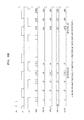
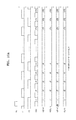
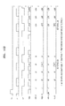
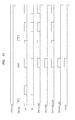
- FIGS. 4A and 4B are timing diagrams illustrating signals output from or measured by the control driver 110.
- the image forming apparatus 100 may determine whether any of the light-emitting element array chips 125 are defective according to a voltage measured at the check terminal.
- FIG. 4A is a timing diagram of an example in which all of the light-emitting element array chips 125 are normal
- FIG. 4B is a timing diagram of an example in which some of the light-emitting element array chips 125 are defective.
- the control driver 110 may output a transfer signal via the ⁇ 1 and ⁇ 2 .
- the control driver 110 may output a start signal via the ⁇ s.
- the control driver 110 may output a data signal via the ⁇ i(n).
- the start signal that is output via the terminal ⁇ s is applied once to start operations of the light-emitting element array chips 125.
- the transfer signal may have two alternate potentials. When a first voltage is a high level voltage, a second voltage is a low level voltage. A first transfer signal that is output via the ⁇ 1 is a signal applied to the odd-numbered transfer elements, and a second transfer signal that is output via the ⁇ 2 is a signal applied to the even-numbered transfer elements.
- the first and second transfer signals have two alternate potentials (i.e., a high level and a low level), and alternate between having a high level and a low level.
- the first and second transfer signals overlap for a predetermined time.
- the first and second transfer signals overlap for a predetermined time so that a transfer element may enter a standby state before operations of a previous transfer element finish.
- the control driver 110 In order to determine the defect of the light-emitting element array chips 125, the control driver 110 outputs a signal causing all of the light-emitting elements to emit light.
- the control driver 110 may output the data signal via the ⁇ i(n) so that all light-emitting elements emit light.
- the control driver 110 detects that check signals related to the light-emitting elements are high. In other words, check signals measured at the ⁇ i(n)_chk are high. Therefore, the control driver 110 may determine that the light-emitting element array chips 125 are normal.
- the control driver 110 may detect that check signals of some of the light-emitting elements are low. In other words, the control driver 110 may detect that voltage measured at the ⁇ i(n)_chk is low.
- FIG. 4B illustrates an example in which a fourth light-emitting element or a fourth transfer element is defective. Since a signal measured at the ⁇ i(n)_chk at a time point when the fourth light-emitting element would have emitted light is low, the control driver 110 may determine that the fourth light-emitting element or the fourth transfer element is defective.
- the operations of the light-emitting element array chips 125 will be described with reference to a first light-emitting element L1.
- a voltage of a data signal output from the ⁇ i(n) is high (3.3V) and a voltage applied to an anode of the first light-emitting element L1 is 3.3V, equal voltages are applied to both sides of the first light-emitting element L 1 , and thus current does not flow. In other words, a loop circuit from the ⁇ i(n) to the anode of the first-lighting element L1 is not formed.
- a voltage of the data line ( ⁇ i_(n)) is equal to the signal (3.3V) applied from the ⁇ i(n), and a voltage (3.3V) equal to that of the data line ( ⁇ i_(n)) is applied to the check terminal ( ⁇ i(n)_chk).
- the control driver 110 detects that the voltage applied to the check terminal ( ⁇ (n)_chk) is 3.3V, the control driver 110 may determine the voltage as a high level voltage.
- a voltage of a data signal output from the ⁇ i(n) is low (oV) and a voltage applied to the anode of the first light-emitting element L1 is 3.3V, current flows through the first light-emitting element L1.
- a loop circuit is formed from the ⁇ i(n) to the anode of the first light-emitting element L1. Therefore a voltage of the data line ( ⁇ i_(n)) is about 1.8V, which is about 1.5V less than the voltage (3.3V) applied from the ⁇ i(n) to the anode of the first light-emitting element L1. Therefore, a voltage (about 1.8V) equal to that of the data line is applied to the check terminal ⁇ i(n)_chk).
- control driver 110 When the control driver 110 detects that the voltage applied to the check terminal ( ⁇ i(n)_chk) is 1.8V, the control driver 110 may determine the voltage as a high level voltage, and may thereby determine that a light-emitting element or a transfer element is normal.
- a voltage of a data signal output from the ⁇ i(n) is low (oV)
- a voltage applied to the anode of the first light-emitting element L1 is 3.3V, and thus current does not flow through the first light-emitting element L1.
- a loop circuit is not formed from the ⁇ i(n) to the anode of the first light-emitting element L1.
- the voltage of the data line ( ⁇ i_(n)) is equal to the voltage (oV) of a signal applied from the ⁇ i(n), and a voltage (oV) equal to that of the ⁇ i(n) is applied to the check terminal ( ⁇ i(n)_chk).
- the control driver 110 detects that the voltage applied to the check terminal ( ⁇ i(n)_chk) is oV, the control driver 110 may determine the voltage as a low level voltage, and determine that the light-emitting element or the transfer element is defective.
- the image forming apparatus 100 may not only determine whether any of the light-emitting element array chips 125 are defective, but also determine a defective light-emitting element or a defective transfer element.
- FIG. 5 is a diagram illustrating the image forming apparatus 100 according to an exemplary embodiment.
- the image forming apparatus 100 includes a comparing unit 520 instead of the buffer 320.
- Operations of the image forming apparatus 100 of FIG. 5 are the same as those of FIG. 3 except for operations of the comparing unit 520.
- a resistor 510 may be provided between the ⁇ i(n) and the data line of the light-emitting element array chips 125 and connected thereto.
- the comparing unit 520 may output a comparison result obtained by comparing a voltage of a data line and a threshold value to a check terminal of the control driver 110.
- the threshold value may be determined with regard to a voltage applied to a cathode of a light-emitting element and voltage drop of the light-emitting element. For example, when a voltage of 3.3V is applied to the cathode of the light-emitting element and the voltage drop of the light-emitting element is 1.5V, the threshold value may be determined as 1.8V or less.
- the comparing unit 520 may output the comparison result as a 1 or o. For example, if the voltage of the data line is greater than the threshold value, the comparing unit 520 may output a 1 to the control driver 110, and if not, may output a o to the control driver 110.
- FIG. 6 is a diagram illustrating a structure of the image forming apparatus 100 according to an exemplary embodiment.
- light-emitting element arrays 127 may be connected in parallel and connected to the check terminal ( ⁇ chk).
- the image forming apparatus 100 may determine whether any of the light-emitting element array chips 125 are defective by analyzing a voltage output via the check terminal. In detail, the image forming apparatus 100 may separately determine whether any of the light-emitting element array chips 125 are defective by applying a signal such that only a light-emitting element array chip to be checked operates among the light-emitting element array chips 125.
- FIG. 7 is a diagram illustrating the image forming apparatus 100 according to an exemplary embodiment.
- each of the light-emitting element array chips 125 includes a transistor 710.
- the image forming apparatus 100 includes a pull-down resistor 720 connected to cathodes of light-emitting elements.
- a base of the transistor 710 may be connected to the cathodes of the light-emitting elements, and emitters of the transistors 710 are connected to the check terminal ( ⁇ i_chk) in parallel.
- the pull-down resistor 720 may be connected to a node 730.
- the pull-down resistor 720 may function in the same way as the OR gate.
- a single check terminal ( ⁇ i_chk) is included in the control driver 110.
- the control driver 110 may analyze a voltage measured at the check terminal to determine whether any of the light-emitting element array chips 125 are defective and determine which transfer element or which light-emitting element is defective.
- the control driver 110 may apply a signal such that only the light-emitting element array chip to be checked among the light-emitting element array chips 125 operates.
- the control driver 110 may apply signals only to the light-emitting element array chip to be checked from among the light-emitting element array chips 125. Therefore, the control driver 110 may monitor a voltage of a data line of the light-emitting element array chip 125 to be checked via the check terminal ⁇ i_chk.
- the transistor 710 may only operate when the light-emitting elements are normal. Since the base of the transistor 710 is connected to the data line, the transistor 710 may operate only when a voltage of the data line is high. The voltage of the data line maintains a high level when all of the light-emitting elements are normal, but maintains a low level when any of the light-emitting elements are defective. For example, when a light-emitting element is defective, a data signal is low, and thus a loop circuit is not formed. As a result, a voltage of a data line also maintains a low level.
- control driver 110 may determine that a light-emitting element array chip is defective when the voltage of a data line corresponding thereto is low, and determine that a light-emitting element is defective based on a time point when the voltage of the data line is measured as low.
- FIGS. 8A and 8B are timing diagrams illustrating operations of the image forming apparatus 100 of FIG. 7 .
- FIG. 8A is a timing diagram of an example in which a third light-emitting element array chip among the light-emitting element array chips 125 is normal
- FIG. 8B is a timing diagram of an example in which fourth and 254th light-emitting elements included in the third light-emitting element array chip among the light-emitting element array chips 125 are defective.
- the control driver 110 checks operations of the third light-emitting element array chip among the light-emitting element array chips 125.
- the control driver 110 may apply a signal such that only the third light-emitting element array chip operates.
- the control driver 110 applies a low level data signal to the light-emitting element array chips 125 except for the third light-emitting element array chip. Therefore, light-emitting elements of the light-emitting element array chips 125 except for the third light-emitting element array chip do not operate.
- the control driver 110 outputs a start signal via the ⁇ s and output transfer signals via the ⁇ 1 and the ⁇ 2.
- the control driver 110 applies a data signal via a ⁇ i(3) such that light-emitting elements included in the third light-emitting element array chip all emit light.
- the control driver 110 applies a low level data signal to ⁇ i(1) to ⁇ i(n) except for the ⁇ i(3). Therefore, a high level voltage is measured at a ⁇ i( 3 )_chk, and a low level voltage is measured at ⁇ (1)_chk to ⁇ i(n)_chk except for the (Di( 3 )_chk.
- the transistors 710 connected in parallel and the pull-down resistor 720 function in the same way as the OR gate. When signals of the ⁇ (1)_chk to ⁇ i(n)_chk are applied to each of the transistors 710, a high level voltage is measured at the Ci_chk because of the high level voltage of the ⁇ i(3)_chk.
- the control driver 110 may apply the same signal as in FIG. 8A .
- FIG. 8B illustrates an example including a defective light-emitting element
- a level of a signal measured at the check terminal is different from that of FIG. 8A .
- a low level voltage is measured at the ⁇ i(3)_chk and low level voltages are measured at the ⁇ (1)_chk to ⁇ i(n)_chk except for the (Di(3)_chk.
- a low level voltage may also be measured at the ⁇ i_chk.
- the control driver 110 may determine that a light-emitting element at a time point when a low level voltage is measured at the Ci_chk is defective.
- FIG. 9 is a diagram illustrating the image forming apparatus 100 according to an exemplary embodiment.
- each of the light-emitting element array chips 125 includes a transistor 910.
- the image forming apparatus 100 includes a pull-up resistor 920 connected to the cathodes of the light-emitting elements.
- a base of the transistor 910 is connected to the cathodes of the light-emitting elements, and collectors of the transistors 910 are connected in parallel.
- ⁇ i(n)_chk indicates a collector of the transistor 910 of an n-th light-emitting element array chip among the light-emitting element array chips 125.
- the collectors of the transistors 910 are connected to the check terminal ( ⁇ i_chk) and the pull-up resistor 920 is connected to a node 930.
- the transistors 910 and the pull-up resistor 920 function in the same way as the AND gate.
- the control driver 110 may apply a data signal to only the light-emitting element array chip 125 to be checked, and apply a low level signal to the light-emitting element array chips 125 except for the light-emitting element array chip 125 to be checked. Therefore, the transistors 910 of the light-emitting element array chips 125 except for the light-emitting element array chip 1250 to be checked do not operate, and the transistor 910 of the light-emitting element array chip 125 to be checked operates according to whether a light-emitting element and a transfer element is normal. When the light-emitting elements included in the light-emitting element array chips 125 are all normal, the transistor 910 operates and current flows from the Vcc to the transistor 910.
- a low level voltage is measured at the check terminal ( ⁇ i_chk).
- the transistor 910 does not operate, and current does not flow from the Vcc to the transistor 910. Therefore, a high level voltage is measured at the check terminal ⁇ i_chk.
- FIGS. 10A and 10B are timing diagrams illustrating operations of the image forming apparatus 100 of FIG. 9 .
- FIG. 10A is a timing diagram of an example in which the third light-emitting element array chip among the light-emitting element array chips 125 is normal
- FIG. 10B is a timing diagram of an example in which the fourth and 254th light-emitting elements included in the third light-emitting element array chip among the light-emitting element array chips 125 are defective.
- the control driver 110 checks operations of the third light-emitting element array chip.
- the control driver 110 applies a signal such that only the third light-emitting element array chip operates.
- the control driver 110 applies a high level data signal to the light-emitting element array chips 125 except for the third light-emitting element array chip.
- the control driver 110 applies the high level data signal to the ⁇ i(1) to ⁇ i(n) except for the ⁇ i(3).
- the light-emitting elements and the transistors 910 of the light-emitting element array chips 125 except for the third light-emitting element array chip do not operate, and a high level voltage is measured at the ⁇ i(1)_chk to ⁇ i(n)_chk except for the ⁇ i(3)_chk.
- the control driver 110 applies a data signal via the ⁇ i(3) such that the light-emitting elements included in the third light-emitting element array chip all emit light. Since the transistor 910 connected to the third light-emitting element array chip operates when the third light-emitting element array chip is normal, a low level voltage is measured at the ⁇ i(3)_chk. However, voltages at the ⁇ (1)_chk to ⁇ i(n)_chk except for the voltage at the ⁇ i(3)_chk have a high level. Therefore, the pull-up resistor 920 and the transistor 910, which are connected in parallel, function in the same way as the AND gate, and thus, a low level voltage is measured at the ⁇ i_chk.
- the control driver 110 may apply the same signal as in FIG. 10A .
- FIG. 10B illustrates an example including a defective light-emitting element
- a level of a signal measured at the check terminal is different from that of FIG. 10A .
- a high level voltage is measured at the ⁇ i(3)_chk and high level voltages are measured at the ⁇ i(1)_chk to ⁇ i(n)_chk except for the (Di(3)_chk.
- the control driver 110 may determine that a light-emitting element at a time point when a high level voltage is measured at the Ci_chk is defective.
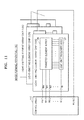
- FIG. 11 is a diagram illustrating a structure of the image forming apparatus 100 according to another exemplary embodiment.
- the image forming apparatus 100 may determine whether any of a plurality of transfer element arrays 126 are defective.
- the plurality of transfer element arrays 126 are connected to a check terminal ( ⁇ chk) in parallel.
- the transfer element arrays 126 that are connected in parallel may be connected to a pull-up resistor, a diode and a pull-up resistor, or a transistor and a pull-up resistor.
- Embodiments will be described in detail with reference to FIGS. 12 to 20 .
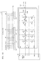
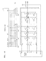
- FIG. 12 is a diagram illustrating the image forming apparatus 100 according to an exemplary embodiment.
- each of the light-emitting element array chips 125 includes a diode 1210.
- the image forming apparatus 100 includes a pull-up resistor 1220 which are connected to a last diode D256 of one of the transfer element arrays 126.
- a cathode of the diode 1210 may be connected to a cathode of the last diode D256, and an anode of the diode 1210 may be connected to the pull-up resistor 1220.
- a node 1240 may be connected to a check terminal ⁇ s_chk), the anode of the diode 1210, and the pull-up resistor 1220.
- the image forming apparatus 100 may determine whether any of the light-emitting element array chips 125 are defective by analyzing a voltage measured at a single check terminal ( ⁇ s_chk). In detail, the image forming apparatus 100 may determine that one of the light-emitting element array chips 125 is defective. That is, the image forming apparatus 100 may determine that one of the light-emitting element array chips 125 includes a defective transfer element.
- a low level signal is output from the node 1240 at a predetermined time point in an n-th light-emitting element array chip from among the light-emitting element array chips 125) that includes at least one defective transfer element. When the image forming apparatus 100 detects a low level signal, the image forming apparatus 100 may determine that one of the light-emitting element array chips 125 is defective and includes a defective transfer element.
- a ⁇ s(n)_chk 1230 represents the cathode of the last diode D256 of the n-th light-emitting element array chip 125.
- the transfer element arrays 126 are connected in parallel at the node 1240.
- the pull-up resistor 1220 connected to the node 1240 functions similarly to the AND gate. In other words, only when all signals input from ⁇ s(1)_chk to ⁇ s(n)_chk connected to the node 1240 are high level voltages, a high level voltage is measured at the check terminal. When a low level voltage is output from at least one node selected from the ⁇ s(i)_chk to the ⁇ (n)_chk, a low level voltage is measured at the check terminal.
- the control may determine that at least one light-emitting element array chip is defective from among n light-emitting element array chips 125. A method of determining whether any of the light-emitting element array chips 125 are defective will be described in detail with reference to FIG. 14 .
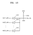
- FIG. 13 is a circuit diagram illustrating a portion of the image forming apparatus 100 of FIG. 12 .
- the ⁇ s(i)_chk represents a cathode of a last diode D256 of a first light-emitting element array chip among the light-emitting element array chips 125
- a ⁇ s(2)_chk represents a cathode of a last diode D256 of a second light-emitting element array chip 125
- the ⁇ s(n)_chk represents a cathode of a last diode D256 of the n-th light-emitting element array chip from among the light-emitting array chips 125.
- the ⁇ s(i)_chk to the ⁇ s(n)_chk are connected to respective diodes 1210, which are inverse diodes, of the light-emitting element array chips 125.
- the pull-up resistor 1220 may function in the same way as the AND gate.
- a Vcc is a high level voltage and levels of voltages of the ⁇ s(i)_chk to the ⁇ s(n)_chk are all high, voltages having the same magnitude are applied to both sides of the diode 1210, and thus current does not flow. Therefore, a high level voltage is measured at the ⁇ s_chk.
- a voltage level of at least one node selected from the ⁇ s(1)_chk to ⁇ s(n)_chk is low, current flows to a low level node. Therefore, a low level voltage is measured at the ⁇ s_chk.
- FIG. 14 is a timing diagram illustrating operations of the image forming apparatus 100 of FIG. 12 .
- FIG. 14 is a timing diagram of an example in which the light-emitting element array chips 125 are all normal.
- the control driver 110 may output a start signal to the transfer element arrays 126.
- the start signal is sequentially shifted from a diode Ds to diodes D1 to D256.
- the control driver 110 may output a transfer signal via ⁇ 1 and ⁇ 2 according to a timing of the start signal.
- FIG. 15 is a timing diagram illustrating operations of the image forming apparatus 100 of FIG. 12 .
- FIG. 15 is a timing diagram illustrating a signal applied and a signal measured to determine whether a first light-emitting element array chip from among the light-emitting array chips 125 is defective.
- the control driver 110 may maintain a start signal at a high level for second to n-th light-emitting element array chips among the light-emitting element array chips 125.
- the control driver 110 input a single pulse signal to the first light-emitting element array chip as the start signal.
- voltages of the ⁇ s(2)_chk to the ⁇ s(n)_chk also have a high level.
- a level of a voltage measured at a check terminal may vary according to a level of a voltage of the ⁇ s(1)_chk.
- the voltage level of the ⁇ s(i)_chk is high, the voltage level measured at the check terminal also is high.
- the voltage level of the ⁇ s(1)_chk is low, the voltage level measured at the check terminal also is low.
- control driver 110 may determine whether transfer elements of the first light-emitting element array chip are normal or defects according to the voltage level measured at the check terminal. In FIG. 15 , since the voltage level of the ⁇ s(1)_chk is high, the voltage level measured at the check terminal is also high.
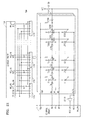
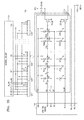
- FIG. 16 is a diagram illustrating the image forming apparatus 100 according to another exemplary embodiment.
- the image forming apparatus 100 determines whether one of the light-emitting element array chips 125 is defective by analyzing a voltage measured at a single check terminal ( ⁇ s_chk). When one of the light-emitting element array chips 125 is defective, the image forming apparatus 100 determines which one of the light-emitting element array chips 125 is defective.
- the image forming apparatus 100 may include a pull-up resistor 1610, without including an inverse diode.
- the image forming apparatus 100 of FIG. 12 includes the diode 1210 that is an inverse diode
- the image forming apparatus 100 of FIG. 16 includes only the pull-up resistor 1610.
- the image forming apparatus 100 of FIG. 16 operates in the same way as the image forming apparatus 100 of FIG. 12 . Therefore, the description of FIG. 12 is also applied to the description of FIG. 16 .
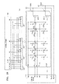
- FIG. 17 is a diagram illustrating the image forming apparatus 100 according to another exemplary embodiment.
- the image forming apparatus 100 may determine whether any of the light-emitting element array chips 125 are defective by analyzing a voltage measured at a single check terminal ( ⁇ s_chk). When one of the light-emitting element array chips 125 is defective, the image forming apparatus 100 determines which one of the light-emitting element array chips 125 is defective. In detail, the image forming apparatus 100 determines a light-emitting element array chip 125 that includes a defective transfer element.
- each of the light-emitting element array chips 125 may include a transistor 1710 connected to a light-emitting element array.
- the image forming apparatus 100 may include a pull-up resistor 1720.
- a base of each of the transistors 1710 is connected to a gate G256 of a last transfer element.
- Collectors of the transistors 1710 are connected in parallel to the pull-up resistor 1720.
- the control driver 110 may determine that a light-emitting element array chip among the light-emitting element array chips 125 includes a defective transfer element by applying a start signal to a light-emitting element array chip to be checked among the light-emitting element array chips 125. In order to determine whether a first light-emitting element array chip is defective, the control driver 110 does not apply a start signal to second to n-th light-emitting element array chips. The control driver 110 applies the start signal only to the first light-emitting element array chip. When transfer elements included in the first light-emitting element array chip are all normal, a high level voltage is transferred to the base of the transistor 1710. Therefore, the transistor 1710 operates, and current flows from a Vcc to emitters of the transistors 1710. Thus, a voltage of a node 1730 is low, and a low level voltage is detected at a check terminal.
- the transistor 1710 when at least one selected from the transfer elements included in the first light-emitting element array chip is defective, voltage is not transferred to the base of the transistor 1710, and thus, the transistor 1710 does not operate. Current does not flow from the Vcc to the transistor 1710, and thus, the voltage of the node 1730 may be a voltage of the Vcc. Therefore, a high level voltage is measured at the check terminal.
- FIGS. 18A and 18B are diagrams illustrating a method of determining whether any of the light-emitting element array chips 125 are defective.
- FIG. 18A is a table showing an example of testing a first light-emitting element array chip from among the light-emitting element array chips 125. Since a start signal is not applied to second to n-th light-emitting element array chips, transfer elements of second to n-th light-emitting element array chips do not operate.
- a voltage of a gate G256 of a last transfer element of each of second to n-th light-emitting element array chips is low, and a voltage of a gate G256 of a last transfer element of the first light-emitting element array chip also is low.
- a high level voltage is measured at the check terminal, and the first light-emitting element array chip is defective.
- the start signal is not transferred to the last transfer element, and thus, the voltage of the gate G256 of the last transfer element of the first light-emitting element array chip is low.
- the voltage of the gate G256 of the last transfer element of each of the second to n-th light-emitting element array chips is low, and the voltage of the gate G256 of the last transfer element of the first light-emitting element array chip is high.
- a low level voltage is measured at the check terminal, and the first light-emitting element array chip is normal.
- the voltage of the gate G256 of the last transfer element of the first light-emitting element array chip is high.
- FIG. 18B illustrates a connection relationship between the transistors 1710 and the pull-up resistor 1720.
- the base of each of the transistors 1710 is connected to the gate G256 of the last transfer element.
- the collectors of the transistors 1710 are connected to the node 1730 in parallel.
- the pull-up resistor 1720 and the ⁇ s_chk are connected to the node 1730.
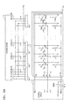
- FIG. 19 is a diagram illustrating the image forming apparatus 100 according to another exemplary embodiment.
- the image forming apparatus 100 includes a pull-down resistor 1920.
- Each of the light-emitting element array chips 125 includes a transistor 1910, and a base of each of the transistors 1910 is connected to a gate G256 of a last transfer element. Emitters of the transistors 1910 are connected in parallel and connected to the pull-down resistor 1920.
- the image forming apparatus 100 of FIG. 19 determines whether any of the light-emitting element array chips 125 are defective similarly as the image forming apparatus 100 of FIG. 17 .
- a connection form of the transistor 1910 is opposite to that of the transistor 1710 of the image forming apparatus 100 of FIG. 17 . Therefore, the method of determining whether the light-emitting element array chips 125 are normal or defective based on a level of a voltage measured at a check terminal, as performed by the image forming apparatus 100 of FIG. 19 , is opposite to that performed by the image forming apparatus 100 of FIG. 17 .
- FIGS. 20A and 20B are diagrams illustrating a method of determining whether any of the light-emitting element array chips 125 are defective.
- FIG. 20A is a table showing an example of testing a first light-emitting element array chip from among the light-emitting element array chips 125. Since a start signal is not applied to second to n-th light-emitting element array chips, transfer elements of the second to n-th light-emitting element array chips do not operate.
- a voltage of a gate G256 of a last transfer element of each of second to n-th light-emitting element array chips is low, and a voltage of a gate G256 of a last transfer element of the first light-emitting element array chip also is low.
- a low level voltage is measured at the check terminal and the first light-emitting element array chip is defective.
- the voltage of the gate G256 of the last transfer element of the first light-emitting element array chip is low.
- the voltage of the gate G256 of the last transfer element of each of second to n-th light-emitting element array chips is low, and a voltage of the gate G256 of the last transfer element of the first light-emitting element array chip is high.
- a high level voltage is measured at the check terminal, and the first light-emitting element array chip is normal.
- the voltage of the gate G256 of the last transfer element of the first light-emitting element array chip is high.
- FIG. 20B illustrates a connection relationship between the transistors 1910 and the pull-down resistor 1920.
- the base of each of the transistors 1910 is connected to the gate G256 of the last transfer element.
- the emitters of the transistors 1910 are connected to a node 1930 in parallel.
- the pull-down resistor 1920 and the ⁇ s_chk are connected to the node 1930.
- FIG. 21 is a diagram illustrating the image forming apparatus 100 according to an exemplary embodiment.
- the image forming apparatus 100 includes a buffer 2110 connected to the light-emitting element arrays 127. Also, the image forming apparatus 100 includes a pull-up resistor 2120 connected to the transfer element arrays 126.
- each of the light-emitting element array chips 125 includes a diode 2130 connected to . Therefore, the image forming apparatus 100 may determine whether a defect is present in the light-emitting elements and the transfer elements.
- the defect is determined by using the same method as described with reference to FIGS. 3 and 12 .
- FIG. 22 is a diagram illustrating the image forming apparatus 100 according to an exemplary embodiment.
- the image forming apparatus 100 includes a buffer 2210 connected to the light-emitting element arrays 127, and each of the transfer element arrays 126 includes a pull-down resistor 2220.
- the transfer element arrays 126 are connected in parallel. Since the pull-down resistors 2220 are connected to a Vga, the pull-down resistors 2220 function in the same way as the OR gate.
- the control driver 110 may apply a signal to only a light-emitting element array chip to be checked from among the light-emitting element array chips 125, and measure a voltage via a check terminal when a 256th transfer element T256 operates. If a high level voltage is measured at the check terminal, the light-emitting element array chips 125 to which the signal is applied are normal, and if not, the light-emitting element array chips 125 to which the signal is applied are defective.
- the method of determining the defect of the light-emitting elements is the same as the method described with reference to FIG. 3 .
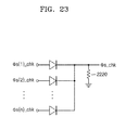
- FIG. 23 is a diagram illustrating a connection relationship between diodes and the pull-down resistor 2220.
- the diodes are connected between the check terminal ⁇ _chk) and a last transfer element of each of the light-emitting element array chips 125.
- the pull-down resistor 2220 is connected between the diodes that are connected to the check terminal in parallel.
- a high level voltage is applied to n terminals ⁇ s(1)_chk to ⁇ s(n)_chk when the transfer element arrays 126 are normal.
- the start signal is transferred from the first to 256th transfer elements, and a high level voltage is applied to the terminal ⁇ s(1)_chk when the start signal is transferred to the 256th transfer element.
- a high level voltage is applied to the terminal ⁇ s(1)_chk, current flows to the pull-down resistor 2220 through a diode connected to the ⁇ s(1)_chk. Therefore, a high level voltage is measured at the ⁇ s_chk.
- the transfer element arrays 126 of the first light-emitting element array chip are defective, the transfer of the start signal is stopped at a defective transfer element, and thus, a low level voltage is transferred to the ⁇ s(i)_chk at a time point when the start signal would have been transferred to the 256th transfer element (that is, voltage is not applied).
- the ⁇ s(i)_chk receives a low level voltage, current does not flow from the ⁇ s(i)_chk to the pull-down resistor 2220. Therefore, a low level voltage is measured at the ⁇ s_chk.
- FIG. 24 is a diagram illustrating the image forming apparatus 100 according to an exemplary embodiment.
- each of the light-emitting element array chips 125 includes a transistor 2410 connected to light-emitting element arrays and a diode 2430 connected to transfer element arrays.
- a pull-down resistor 2420 is connected to the respective transistors 2410 of the light-emitting element array chips 125, and a pull-up resistor 2440 is connected to the respective diodes 2430 of the light-emitting element array chips 125.
- the image forming apparatus 100 of FIG. 24 is a combination of the image forming apparatuses 100 shown in FIGS. 7 and 12 , defects are determined by using the same method as described with reference to FIGS. 7 and 12 .
- FIG. 25 is a diagram illustrating the image forming apparatus 100 according to an exemplary embodiment.
- each of the light-emitting element array chips 125 includes a transistor 2510 connected to light-emitting element arrays and a transistor 2530 connected to transfer element arrays.
- a pull-down resistor 2520 is connected to the respective transistors 2510 of the light-emitting element array chips 125, and a pull-up resistor 2540 is connected to the respective transistors 2530 of the light-emitting element array chips 125.
- the image forming apparatus 100 of FIG. 25 is a combination of the image forming apparatuses 100 shown in FIGS. 7 and 17 , defects are determined by using the same method as described with reference to FIGS. 7 and 17 .
- FIG. 26 is a diagram illustrating the image forming apparatus 100 according to an exemplary embodiment.
- each of the light-emitting element array chips 125 includes a transistor 2610 connected to light-emitting element arrays and a transistor 2630 connected to transfer element arrays.
- a pull-down resistor 2620 is connected to the respective transistors 2610 of the light-emitting element array chips 125, and a pull-down resistor 2640 is connected to the respective transistors 2630 of the light-emitting element array chips 125.
- the image forming apparatus 100 of FIG. 26 is a combination of the image forming apparatuses 100 shown in FIGS. 7 and 19 , defects are determined by using the same method as described with reference to FIGS. 7 and 19 .
- FIG. 27 is a diagram illustrating the image forming apparatus 100 according to an exemplary embodiment.
- each of the light-emitting element array chips 125 includes a transistor 2710 connected to light-emitting element arrays and a diode 2730 connected to transfer element arrays.
- a pull-up resistor 2720 is connected to the respective transistors 2710 of the light-emitting element array chips 125, and a pull-up resistor 2740 is connected to respective diodes 2730 of the light-emitting element array chips 125.
- the image forming apparatus 100 of FIG. 27 is a combination of the image forming apparatuses 100 shown in FIGS. 9 and 12 , defects are determined by using the same method as described with reference to FIGS. 9 and 12 .
- FIG. 28 is a diagram illustrating the image forming apparatus 100 according to an exemplary embodiment.
- each of the light-emitting element array chips 125 includes a transistor 2810 connected to light-emitting element arrays and a transistor 2830 connected to transfer element arrays.
- a pull-up resistor 2820 is connected to the respective transistors 2810 of the light-emitting element array chips 125, and a pull-up resistor 2840 is connected to the respective transistors 2830 of the light-emitting element array chips 125.
- the image forming apparatus 100 of FIG. 28 is a combination of the image forming apparatuses 100 shown in FIGS. 9 and 17 , defects are determined by using the same method as described with reference to FIGS. 9 and 17 .
- FIG. 29 is a diagram illustrating the image forming apparatus 100 according to another exemplary embodiment.
- the control driver 110 may include a buffer 2920 and a resistor 2910.
- FIG. 3 illustrates that the buffer 320 and the resistor 310 of the image forming apparatus 100 are connected between the control driver 110 and the light-emitting element array chips 125
- FIG. 29 illustrates that the buffer 2920 and the resistor 2910 of the image forming apparatus 100 are included in the control driver 110.
- the image forming apparatus 100 of FIG. 29 is the same as the image forming apparatus 100 of FIG. 3 except that the control driver 110 includes the buffer 2920 and the resistor 2910.
- control driver 110 may include not only the buffer 2910, but also, a comparing unit, a transistor, a diode, a pull-up resistor, or a pull-down resistor.
- an image forming apparatus may determine a defective light-emitting element array chip from a plurality of light-emitting element array chips.
- the image forming apparatus may determine whether a transfer element or a light-emitting element is defective.
- the image forming apparatus may apply a signal to the transfer element or the light-emitting element, analyze an amplitude of a signal output from the transfer element or the light-emitting element, and thus determine the defective light-emitting element array chip.
- the device described herein may include a processor, a memory for storing program data and executing it, a permanent storage unit such as a disk drive, a communication port for handling communications with external devices, and user interface devices, including a touch panel, keys, buttons, etc.
- these software modules may be stored as program instructions or computer readable codes executable on a processor on a computer-readable medium.
- the computer readable recording medium include magnetic storage media (e.g., ROM, floppy disks, or hard disks), and optical recording media (e.g., CD-ROMs or DVDs).
- the computer readable recording medium can also be distributed over network coupled computer systems so that the computer readable code is stored and executed in a distributive manner. This media can be read by the computer, stored in the memory, and executed by the processor.
- inventive concept may be described in terms of functional block components and various processing steps. Such functional blocks may be realized by any number of hardware and/or software components configured to perform the specified functions.
- inventive concept may employ various integrated circuit (IC) components, e.g., memory elements, processing elements, logic elements, look-up tables, and the like, which may carry out a variety of functions under the control of one or more microprocessors or other control devices.
- IC integrated circuit
- the inventive concept may be implemented with any programming or scripting language such as C, C++, Java, assembler language, or the like, with the various algorithms being implemented with any combination of data structures, objects, processes, routines or other programming elements.
- Functional aspects may be implemented in algorithms that are executed on one or more processors.
- inventive concept could employ any number of conventional techniques for electronics configuration, signal processing and/or control, data processing and the like.
- the words “mechanism,” “element,” “means,” and “configuration” are used broadly and are not limited to mechanical or physical embodiments, but can include software routines in conjunction with processors, etc.
Landscapes
- Physics & Mathematics (AREA)
- General Physics & Mathematics (AREA)
- Engineering & Computer Science (AREA)
- Multimedia (AREA)
- Signal Processing (AREA)
- Optics & Photonics (AREA)
- Health & Medical Sciences (AREA)
- General Health & Medical Sciences (AREA)
- Toxicology (AREA)
- Printers Or Recording Devices Using Electromagnetic And Radiation Means (AREA)
- Led Devices (AREA)
- Control Of Indicators Other Than Cathode Ray Tubes (AREA)
Abstract
Description
- The present invention relates to an image forming apparatus, particularly to an image forming apparatus capable of determining whether any of light-emitting element array chips are defective.
- An image forming apparatus using light-emitting element array chips receives print data from a personal computer (PC) and forms an image by using light-emitting elements. When the light-emitting elements emit light, an electrostatic latent image is formed on a photoconductor drum in the image forming apparatus. Thereafter, a print image is output through development, transfer, and fusing processes.
- A light-emitting element array chip included among the light-emitting element array chips may be defective. Light-emitting elements of a defective light-emitting element array chip may not emit light, thus causing an error. That is, printing data not being printed on paper.
- One or more exemplary embodiments include an image forming apparatus capable of determining whether any of light-emitting element array chips are defective.
- Additional aspects will be set forth in part in the description which follows and, in part, will be apparent from the description, or may be learned by practice of the presented exemplary embodiments.
- According to one or more exemplary embodiments, an image forming apparatus includes a plurality of light-emitting element array chips including a light-emitting element array and a transfer element array; and a control driver applying a signal to the plurality of light-emitting element array chips. The control driver includes a check terminal that measures signals output from the plurality of light-emitting element array chips, and the control driver determines whether any of the plurality of light-emitting element array chips are defective by analyzing the signals measured at the check terminal.
- According to one or more exemplary embodiments, an image forming apparatus includes a plurality light-emitting element array chips including a light-emitting element array and a transfer element array, and a control driver applying a signal to the light-emitting element array chips. Light-emitting element arrays included in the plurality of light-emitting element array chips are connected in parallel, and the control driver determines whether any of the light-emitting element arrays are defective by analyzing signals output from the light-emitting element arrays that are connected in parallel.
- These and/or other aspects will become apparent and more readily appreciated from the following description of the exemplary embodiments, taken in conjunction with the accompanying drawings in which:
-
FIG. 1 is a diagram illustrating an exemplary process of outputting an image by using light-emitting element array chips; -
FIGS. 2 and3 are diagrams illustrating image forming apparatuses according to exemplary embodiments; -
FIGS. 4A and4B are timing diagrams illustrating signals output from or measured by a control driver; -
FIGS. 5 to 7 are diagrams illustrating image forming apparatuses according to exemplary embodiments; -
FIGS. 8A and8B are timing diagrams illustrating operations of the image forming apparatus ofFIG. 7 ; -
FIG. 9 is a diagram illustrating an image forming apparatus according to an exemplary embodiment; -
FIGS. 10A and10B are timing diagrams illustrating operations of the image forming apparatus ofFIG. 9 ; -
FIG. 11 is a diagram illustrating a structure of an image forming apparatus according to another exemplary embodiment; -
FIG. 12 is a diagram illustrating an image forming apparatus according to an exemplary embodiment; -
FIG. 13 is a circuit diagram illustrating a portion of the image forming apparatus ofFIG. 12 ; -
FIGS. 14 and15 are timing diagrams illustrating operations of the image forming apparatus ofFIG. 12 ; -
FIGS. 16 and17 are diagrams illustrating an image forming apparatus according to further exemplary embodiments; -
FIGS. 18A and 18B are diagrams illustrating a method of determining whether any of light-emitting element array chips are defective; -
FIG. 19 is a diagram illustrating an image forming apparatus according to another exemplary embodiment; -
FIGS. 20A and 20B are diagrams illustrating a method of determining whether any of light-emitting element array chips are defective; -
FIGS. 21 and22 are diagrams illustrating image forming apparatuses according to exemplary embodiments; -
FIG. 23 is a diagram illustrating a connection relationship between diodes and a pull-down resistor; -
FIGS. 24 to 29 are diagrams illustrating image forming apparatuses according to various exemplary embodiments. - Referring to
FIG. 1 , upon receiving print data from a personal computer (PC) 50, an image forming apparatus may perform operations for outputting an image. - The image forming apparatus may form an electrostatic latent image on a
photoconductor drum 300 by using light-emitting elements and output an image through development, transfer, and fusingprocesses including electrification 1,exposure 2,development 3,transfer 4, fusing 5. - The image forming apparatus may include a
control driver 110, achip array 120, alens array 200, and thephotoconductor drum 300. - The
control driver 110 may control thechip array 120 according to the print data received from the PC 50. Thechip array 120 may include a plurality of light-emitting element array chips. Thecontrol driver 110 may separately control the light-emitting element array chips. - The
lens array 200 may be arranged in an axial direction (i.e., a main scanning direction) of thephotoconductor drum 300. Light having passed through thelens array 200 may form an image on a surface of thephotoconductor drum 300. - The
photoconductor drum 300 may be exposed to light to form an electrostatic latent image. A developer (not shown) may develop the electrostatic latent image formed on thephotoconductor drum 300. -
FIG. 2 is a diagram illustrating animage forming apparatus 100 according to an exemplary embodiment. Referring toFIG. 2 , theimage forming apparatus 100 includes acontrol driver 110 and a plurality of light-emittingelement array chips 125. - The
control driver 110 determines whether any of the light-emittingelement array chips 125 are defective. Thecontrol driver 110 determines whether any of the light-emittingelement array chips 125 are defective, determines which of the light-emittingelement array chips 125 are defective, and determines which light-emitting elements or which transfer elements are defective in the light-emittingelement array chips 125. - The
control driver 110 includes a check terminal that measures signals output from the light-emittingelement array chips 125, analyzes the signals measured at the check terminal, and determines whether any of the light-emittingelement array chips 125 are defective. A method of determining whether any of the light-emittingelement array chips 125 are defective, which may be performed by thecontrol driver 110, will be described in detail below. - The
control driver 110 includes a terminal that outputs signals and a terminal that receives signals. In other words, thecontrol driver 110 includes a terminal that outputs signals for controlling a transfer element or a light-emitting element and a terminal that receives signals from the transfer element or the light-emitting element. Thecontrol driver 110 may include at least one check terminal for determining whether any of the light-emittingelement array chips 125 are defective. - The
control driver 110 receives print data and operates according to the received print data. Thecontrol driver 110 receives the print data from a main board or a central processing unit (CPU) included in theimage forming apparatus 100, and controls on/off of the light-emitting elements according to the received print data. The print data is data representing an image to be formed. - The
control driver 110 may be software that is executed by at least one processor. Alternatively, thecontrol driver 110 may be hardware such as a control driver. - Each of the light-emitting
element array chips 125 includes a transfer element array and a light-emitting element array. The transfer element array includes include a plurality of transfer elements, and the light-emitting element array includes a plurality of light-emitting elements. The transfer elements may sequentially turn the light-emitting elements on and off. The transfer elements and the light-emitting elements may be one-to-one matched. Light emission conditions of the light-emitting elements may be determined according to states of the transfer elements. In order for a light-emitting element to emit light, a transfer element corresponding to the light-emitting element has to be in a standby state. When the transfer element is in a standby state, the on/off of the light-emitting element may be determined according to a data signal input to the light-emitting element. When a start signal is input to the transfer elements, the transfer elements may sequentially enter a standby signal according to a transfer signal. - The light-emitting element array chips 125 receive signals from the
control driver 110 and operate according to the received signals. The light-emitting element array chips 125 may be separately controlled by thecontrol driver 110. - The light-emitting element array chips 125 may be connected in parallel. Data lines of the light-emitting element array chips 125 may be connected in parallel, and gates of last transfer elements of the transfer element arrays may be connected in parallel.
-
FIG. 3 is a diagram illustrating theimage forming apparatus 100 according to an exemplary embodiment. Referring toFIG. 3 , theimage forming apparatus 100 may determine whether any of the light-emitting element array chips 125 are defective. Theimage forming apparatus 100 may separately apply data signals to the light-emitting element array chips 125, and determine whether any one of the light-emitting element array chips 125 are defective by analyzing signals measured at a check terminal (Φi(n)_chk) connected to each of the light-emitting element array chips 125. - The light-emitting elements may be light-emitting thyristors, and the transfer elements may be transfer thyristors. A thyristor has a PNPN junction and includes a gate. For example, each of the light-emitting element array chips 125 may include 256 thyristors. T1 to T256 refer to the transfer thyristors and L1 to L256 refer to the light-emitting thyristors. D1 to D256 refer to diodes connected to the transfer thyristors. G1 to G256 refer to gates of the transfer thyristors. When a voltage of a predetermined level or more is applied to a gate of a thyristor, since a breakdown voltage of the thyristor is lowered, an operation voltage of the thyristor is lowered. Thus, by applying a voltage to the gate of the thyristor, the thyristors may be operated by a lower driving voltage.
- The transfer thyristors enter an operating state according to a start signal and transfer signals (Φ1 signal and Φ2 signal). For example, when the start signal is applied to the gate G1 of the transfer thyristor T1 and a transfer signal (Φ1 signal) is applied to the transfer thyristor T1, the transfer thyristor T1 enters an operating state.
- When the transfer thyristor T1 is in the operating state, the light-emitting thyristor L1 enters a light-emitting state. The gate G1 of the transfer thyristor T1 is equal to a gate of the light-emitting thyristor L1. Therefore, when the transfer thyristor T1 enters the operating state, the light-emitting thyristor L1 also enters the operating state. When the light-emitting thyristor L1 is in the operating state, the light-emitting thyristor L1 emits light according to a data signal input to a terminal Φi.
- By repetition of the process above, the transfer thyristors T1 to T256 sequentially enter the operating state, the light-emitting thyristors L1 to L256 also enter the operating state, and the light-emitting thyristors L1 to L256 sequentially emit or not emit light.
- Terminals of the
image forming apparatus 100 illustrated inFIG. 3 will be described below. Φ1 refers to a terminal that outputs signals for controlling odd-numbered transfer elements, and Φ2 refers to a terminal that outputs signals for controlling even-numbered transfer elements. Φs refers to a terminal that outputs signals for controlling an operation start time of the transfer elements. Φi(n) refers to a terminal that is connected to an n-th light-emittingelement array chip 125 and outputs data signals. Thecontrol driver 110 includes n terminals Φi(n). Φi(n)_chk refers to a check terminal that is connected to the n-th light-emitting element array chip among light-emitting element array chips 125 and data lines of the light-emitting elements. Thecontrol driver 110 includes n check terminals Φi(n)_chk. The Φi(n)_chk and the Φi(n) are connected in parallel. Φi_(n) refers to a node connected to a cathode of an n-th light-emitting element. Vga refers to ground. - The
image forming apparatus 100 includes abuffer 320 and aresistor 310. Thebuffer 320 is connected between thecontrol driver 110 and the light-emitting element array chips 125, and connected between the Φi(n)_chk and the data lines of the light-emitting element array chips 125. Also, theresistor 310 may be provided between the Φi(n) and the data line of the light-emittingelement array chip 125 and connected thereto. Thebuffer 320 may be separately connected to each of the light-emitting element array chips 125. Thebuffer 320 may output a voltage of a data line to the check terminal. Theresistor 310 formed in a loop circuit may drop voltages when current flows. Accordingly, the voltage of the data line may change based on whether or not a loop circuit is formed, the check terminal may measure the voltage of the data line, and thecontrol driver 110 may determine whether any of the light-emitting element array chips 125 are defective by analyzing the voltage measured at the check terminal. - Each of the light-emitting element array chips 125 is connected to the
control driver 110. Φi(n) refers a terminal that is connected to the n-th light-emittingelement array chip 125, and Φi_(n) refers to a data line of the n-th light-emittingelement array chip 125. - The
control driver 110 determines whether any of the light-emitting element array chips 125 are defective by analyzing a signal measured at the check terminal (Φi(n)_chk). In detail, thecontrol driver 110 may analyze a voltage measured at Φi(n)_chk, and thus determine whether any of the light-emitting element array chips 125 are defective. The defective light-emitting element array chip refers to a light-emitting element array chip having at least one light-emitting element that does not emit light. There may be two cases in which a light-emitting element is unable to emit light. First, the light-emitting element may be unable to emit light because the light-emitting element itself is defective. Second, the light-emitting element may be unable to emit light because a transfer element connected to the light-emitting element is defective. When the transfer element is defective, voltage is not supplied to a gate of the light-emitting element, and thus, the light-emitting element does not operate even when a data signal is applied to the light-emitting element. - The
control driver 110 determines whether any of the light-emitting element array chips 125 are defective by analyzing a voltage level measured at the check terminal. For example, when all of the light-emitting element array chips 125 are normal, the voltage level measured at the check terminal is high. When at least one of the light-emitting element array chips 125 is defective, some voltage levels measured at the check terminal Φi(n)_chk are low. - The
control driver 110 may measure a voltage via the check terminal as a data signal is applied, and when a low level signal is detected, thecontrol driver 110 may determine that at least one of the light-emitting element array chips 125 is defective. Also, thecontrol driver 110 may determine a time point when the low level signal is detected, and thereby determine a defective light-emitting element or a defective transfer element. -
FIGS. 4A and4B are timing diagrams illustrating signals output from or measured by thecontrol driver 110. Referring toFIGS. 4A and4B , theimage forming apparatus 100 may determine whether any of the light-emitting element array chips 125 are defective according to a voltage measured at the check terminal.FIG. 4A is a timing diagram of an example in which all of the light-emitting element array chips 125 are normal, andFIG. 4B is a timing diagram of an example in which some of the light-emitting element array chips 125 are defective. - The
control driver 110 may output a transfer signal via the Φ1 and Φ2. Thecontrol driver 110 may output a start signal via the Φs. Thecontrol driver 110 may output a data signal via the Φi(n). - The start signal that is output via the terminal Φs is applied once to start operations of the light-emitting element array chips 125.
- The transfer signal may have two alternate potentials. When a first voltage is a high level voltage, a second voltage is a low level voltage. A first transfer signal that is output via the Φ1 is a signal applied to the odd-numbered transfer elements, and a second transfer signal that is output via the Φ2 is a signal applied to the even-numbered transfer elements. The first and second transfer signals have two alternate potentials (i.e., a high level and a low level), and alternate between having a high level and a low level. The first and second transfer signals overlap for a predetermined time. The first and second transfer signals overlap for a predetermined time so that a transfer element may enter a standby state before operations of a previous transfer element finish.
- In order to determine the defect of the light-emitting element array chips 125, the
control driver 110 outputs a signal causing all of the light-emitting elements to emit light. In detail, thecontrol driver 110 may output the data signal via the Φi(n) so that all light-emitting elements emit light. - In
FIG. 4A , thecontrol driver 110 detects that check signals related to the light-emitting elements are high. In other words, check signals measured at the Φi(n)_chk are high. Therefore, thecontrol driver 110 may determine that the light-emitting element array chips 125 are normal. - In
FIG. 4B , thecontrol driver 110 may detect that check signals of some of the light-emitting elements are low. In other words, thecontrol driver 110 may detect that voltage measured at the Φi(n)_chk is low.FIG. 4B illustrates an example in which a fourth light-emitting element or a fourth transfer element is defective. Since a signal measured at the Φi(n)_chk at a time point when the fourth light-emitting element would have emitted light is low, thecontrol driver 110 may determine that the fourth light-emitting element or the fourth transfer element is defective. - The operations of the light-emitting element array chips 125 will be described with reference to a first light-emitting element L1. When a voltage of a data signal output from the Φi(n) is high (3.3V) and a voltage applied to an anode of the first light-emitting element L1 is 3.3V, equal voltages are applied to both sides of the first light-emitting element L1, and thus current does not flow. In other words, a loop circuit from the Φi(n) to the anode of the first-lighting element L1 is not formed. Therefore, a voltage of the data line (Φi_(n)) is equal to the signal (3.3V) applied from the Φi(n), and a voltage (3.3V) equal to that of the data line (Φi_(n)) is applied to the check terminal (Φi(n)_chk). When the
control driver 110 detects that the voltage applied to the check terminal (Φ(n)_chk) is 3.3V, thecontrol driver 110 may determine the voltage as a high level voltage. - When a voltage of a data signal output from the Φi(n) is low (oV) and a voltage applied to the anode of the first light-emitting element L1 is 3.3V, current flows through the first light-emitting element L1. In other words, a loop circuit is formed from the Φi(n) to the anode of the first light-emitting element L1. Therefore a voltage of the data line (Φi_(n)) is about 1.8V, which is about 1.5V less than the voltage (3.3V) applied from the Φi(n) to the anode of the first light-emitting element L1. Therefore, a voltage (about 1.8V) equal to that of the data line is applied to the check terminal Φi(n)_chk). When the
control driver 110 detects that the voltage applied to the check terminal (Φi(n)_chk) is 1.8V, thecontrol driver 110 may determine the voltage as a high level voltage, and may thereby determine that a light-emitting element or a transfer element is normal. - When a light-emitting element (L1) or a transfer element (T1) is defective, a voltage of a data signal output from the Φi(n) is low (oV), and a voltage applied to the anode of the first light-emitting element L1 is 3.3V, and thus current does not flow through the first light-emitting element L1. In other words, a loop circuit is not formed from the Φi(n) to the anode of the first light-emitting element L1. Therefore, the voltage of the data line (Φi_(n)) is equal to the voltage (oV) of a signal applied from the Φi(n), and a voltage (oV) equal to that of the Φi(n) is applied to the check terminal (Φi(n)_chk). When the
control driver 110 detects that the voltage applied to the check terminal (Φi(n)_chk) is oV, thecontrol driver 110 may determine the voltage as a low level voltage, and determine that the light-emitting element or the transfer element is defective. - According to the method above, the
image forming apparatus 100 may not only determine whether any of the light-emitting element array chips 125 are defective, but also determine a defective light-emitting element or a defective transfer element. -
FIG. 5 is a diagram illustrating theimage forming apparatus 100 according to an exemplary embodiment. Referring toFIG. 5 , theimage forming apparatus 100 includes a comparingunit 520 instead of thebuffer 320. Operations of theimage forming apparatus 100 ofFIG. 5 are the same as those ofFIG. 3 except for operations of the comparingunit 520. Aresistor 510 may be provided between the Φi(n) and the data line of the light-emitting element array chips 125 and connected thereto. - The comparing
unit 520 may output a comparison result obtained by comparing a voltage of a data line and a threshold value to a check terminal of thecontrol driver 110. The threshold value may be determined with regard to a voltage applied to a cathode of a light-emitting element and voltage drop of the light-emitting element. For example, when a voltage of 3.3V is applied to the cathode of the light-emitting element and the voltage drop of the light-emitting element is 1.5V, the threshold value may be determined as 1.8V or less. - The comparing
unit 520 may output the comparison result as a 1 or o. For example, if the voltage of the data line is greater than the threshold value, the comparingunit 520 may output a 1 to thecontrol driver 110, and if not, may output a o to thecontrol driver 110. -
FIG. 6 is a diagram illustrating a structure of theimage forming apparatus 100 according to an exemplary embodiment. Referring toFIG. 6 , light-emittingelement arrays 127 may be connected in parallel and connected to the check terminal (Φchk). Theimage forming apparatus 100 may determine whether any of the light-emitting element array chips 125 are defective by analyzing a voltage output via the check terminal. In detail, theimage forming apparatus 100 may separately determine whether any of the light-emitting element array chips 125 are defective by applying a signal such that only a light-emitting element array chip to be checked operates among the light-emitting element array chips 125. -
FIG. 7 is a diagram illustrating theimage forming apparatus 100 according to an exemplary embodiment. Referring toFIG. 7 , in theimage forming apparatus 100, each of the light-emitting element array chips 125 includes atransistor 710. Theimage forming apparatus 100 includes a pull-down resistor 720 connected to cathodes of light-emitting elements. A base of thetransistor 710 may be connected to the cathodes of the light-emitting elements, and emitters of thetransistors 710 are connected to the check terminal (Φi_chk) in parallel. The pull-down resistor 720 may be connected to anode 730. The pull-down resistor 720 may function in the same way as the OR gate. Therefore, when a high level signal is output from the light-emitting element array chip to be checked among the light-emitting element array chips 125 and low level signals are output from the remaining ones of the light-emitting element array chips 125, the signal measured at the check terminal is high. - A single check terminal (Φi_chk) is included in the
control driver 110. Thecontrol driver 110 may analyze a voltage measured at the check terminal to determine whether any of the light-emitting element array chips 125 are defective and determine which transfer element or which light-emitting element is defective. - The
control driver 110 may apply a signal such that only the light-emitting element array chip to be checked among the light-emitting element array chips 125 operates. Thecontrol driver 110 may apply signals only to the light-emitting element array chip to be checked from among the light-emitting element array chips 125. Therefore, thecontrol driver 110 may monitor a voltage of a data line of the light-emittingelement array chip 125 to be checked via the check terminal Φi_chk. - The
transistor 710 may only operate when the light-emitting elements are normal. Since the base of thetransistor 710 is connected to the data line, thetransistor 710 may operate only when a voltage of the data line is high. The voltage of the data line maintains a high level when all of the light-emitting elements are normal, but maintains a low level when any of the light-emitting elements are defective. For example, when a light-emitting element is defective, a data signal is low, and thus a loop circuit is not formed. As a result, a voltage of a data line also maintains a low level. Therefore, thecontrol driver 110 may determine that a light-emitting element array chip is defective when the voltage of a data line corresponding thereto is low, and determine that a light-emitting element is defective based on a time point when the voltage of the data line is measured as low. -
FIGS. 8A and8B are timing diagrams illustrating operations of theimage forming apparatus 100 ofFIG. 7 .FIG. 8A is a timing diagram of an example in which a third light-emitting element array chip among the light-emitting element array chips 125 is normal, andFIG. 8B is a timing diagram of an example in which fourth and 254th light-emitting elements included in the third light-emitting element array chip among the light-emitting element array chips 125 are defective. - Referring to
FIG. 8A , thecontrol driver 110 checks operations of the third light-emitting element array chip among the light-emitting element array chips 125. Thecontrol driver 110 may apply a signal such that only the third light-emitting element array chip operates. Thecontrol driver 110 applies a low level data signal to the light-emitting element array chips 125 except for the third light-emitting element array chip. Therefore, light-emitting elements of the light-emitting element array chips 125 except for the third light-emitting element array chip do not operate. Thecontrol driver 110 outputs a start signal via the Φs and output transfer signals via the Φ1 and the Φ2. Since the third light-emitting element array chip will be checked, thecontrol driver 110 applies a data signal via a Φi(3) such that light-emitting elements included in the third light-emitting element array chip all emit light. Thecontrol driver 110 applies a low level data signal to Φi(1) to Φi(n) except for the Φi(3). Therefore, a high level voltage is measured at a Φi(3)_chk, and a low level voltage is measured at Φ(1)_chk to Φi(n)_chk except for the (Di(3)_chk. Thetransistors 710 connected in parallel and the pull-down resistor 720 function in the same way as the OR gate. When signals of the Φ(1)_chk to Φi(n)_chk are applied to each of thetransistors 710, a high level voltage is measured at the Ci_chk because of the high level voltage of the Φi(3)_chk. - Referring to
FIG. 8B , thecontrol driver 110 may apply the same signal as inFIG. 8A . However, sinceFIG. 8B illustrates an example including a defective light-emitting element, a level of a signal measured at the check terminal is different from that ofFIG. 8A . At a time point when the fourth and 254th light-emitting elements of the third light-emitting element array chip emit light, a low level voltage is measured at the Φi(3)_chk and low level voltages are measured at the Φ(1)_chk to Φi(n)_chk except for the (Di(3)_chk. Therefore, since the voltages of the Φ(1)_chk to Φi(n)_chk are all low, a low level voltage may also be measured at the Φi_chk.Thecontrol driver 110 may determine that a light-emitting element at a time point when a low level voltage is measured at the Ci_chk is defective. -
FIG. 9 is a diagram illustrating theimage forming apparatus 100 according to an exemplary embodiment. Referring toFIG. 9 , in theimage forming apparatus 100, each of the light-emitting element array chips 125 includes atransistor 910. Theimage forming apparatus 100 includes a pull-upresistor 920 connected to the cathodes of the light-emitting elements. A base of thetransistor 910 is connected to the cathodes of the light-emitting elements, and collectors of thetransistors 910 are connected in parallel. Φi(n)_chk indicates a collector of thetransistor 910 of an n-th light-emitting element array chip among the light-emitting element array chips 125. The collectors of thetransistors 910 are connected to the check terminal (Φi_chk) and the pull-upresistor 920 is connected to anode 930. Thetransistors 910 and the pull-upresistor 920 function in the same way as the AND gate. - The
control driver 110 may apply a data signal to only the light-emittingelement array chip 125 to be checked, and apply a low level signal to the light-emitting element array chips 125 except for the light-emittingelement array chip 125 to be checked. Therefore, thetransistors 910 of the light-emitting element array chips 125 except for the light-emitting element array chip 1250 to be checked do not operate, and thetransistor 910 of the light-emittingelement array chip 125 to be checked operates according to whether a light-emitting element and a transfer element is normal. When the light-emitting elements included in the light-emitting element array chips 125 are all normal, thetransistor 910 operates and current flows from the Vcc to thetransistor 910. Therefore, a low level voltage is measured at the check terminal (Φi_chk). Alternatively, when at least one light-emitting element included in the light-emittingelement array chip 125 to be checked is defective, thetransistor 910 does not operate, and current does not flow from the Vcc to thetransistor 910. Therefore, a high level voltage is measured at the check terminal Φi_chk. -
FIGS. 10A and10B are timing diagrams illustrating operations of theimage forming apparatus 100 ofFIG. 9 .FIG. 10A is a timing diagram of an example in which the third light-emitting element array chip among the light-emitting element array chips 125 is normal, andFIG. 10B is a timing diagram of an example in which the fourth and 254th light-emitting elements included in the third light-emitting element array chip among the light-emitting element array chips 125 are defective. - Referring to
FIG. 10A , thecontrol driver 110 checks operations of the third light-emitting element array chip. Thecontrol driver 110 applies a signal such that only the third light-emitting element array chip operates. Thecontrol driver 110 applies a high level data signal to the light-emitting element array chips 125 except for the third light-emitting element array chip. In detail, thecontrol driver 110 applies the high level data signal to the Φi(1) to Φi(n) except for the Φi(3). Therefore, the light-emitting elements and thetransistors 910 of the light-emitting element array chips 125 except for the third light-emitting element array chip do not operate, and a high level voltage is measured at the Φi(1)_chk to Φi(n)_chk except for the Φi(3)_chk. - Since the third light-emitting element array chip will be checked, the
control driver 110 applies a data signal via the Φi(3) such that the light-emitting elements included in the third light-emitting element array chip all emit light. Since thetransistor 910 connected to the third light-emitting element array chip operates when the third light-emitting element array chip is normal, a low level voltage is measured at the Φi(3)_chk. However, voltages at the Φ(1)_chk to Φi(n)_chk except for the voltage at the Φi(3)_chk have a high level. Therefore, the pull-upresistor 920 and thetransistor 910, which are connected in parallel, function in the same way as the AND gate, and thus, a low level voltage is measured at the Φi_chk. - Referring to
FIG. 10B , thecontrol driver 110 may apply the same signal as inFIG. 10A . However, sinceFIG. 10B illustrates an example including a defective light-emitting element, a level of a signal measured at the check terminal is different from that ofFIG. 10A . At a time point when the fourth and 254th light-emitting elements of the third light-emitting element array chip emit light, a high level voltage is measured at the Φi(3)_chk and high level voltages are measured at the Φi(1)_chk to Φi(n)_chk except for the (Di(3)_chk. Therefore, since the voltages of the Φ(1)_chk to Φi(n)_chk all have a high level, a high level voltage is also measured at the Φi_chk.Thecontrol driver 110 may determine that a light-emitting element at a time point when a high level voltage is measured at the Ci_chk is defective. -
FIG. 11 is a diagram illustrating a structure of theimage forming apparatus 100 according to another exemplary embodiment. Referring toFIG. 11 , theimage forming apparatus 100 may determine whether any of a plurality oftransfer element arrays 126 are defective. In theimage forming apparatus 100 according to the embodiment illustrated inFIG. 11 , the plurality oftransfer element arrays 126 are connected to a check terminal (Φchk) in parallel. Thetransfer element arrays 126 that are connected in parallel may be connected to a pull-up resistor, a diode and a pull-up resistor, or a transistor and a pull-up resistor. Embodiments will be described in detail with reference toFIGS. 12 to 20 . -
FIG. 12 is a diagram illustrating theimage forming apparatus 100 according to an exemplary embodiment. Referring toFIG. 12 , in theimage forming apparatus 100, each of the light-emitting element array chips 125 includes adiode 1210. Theimage forming apparatus 100 includes a pull-upresistor 1220 which are connected to a last diode D256 of one of thetransfer element arrays 126. A cathode of thediode 1210 may be connected to a cathode of the last diode D256, and an anode of thediode 1210 may be connected to the pull-upresistor 1220. Anode 1240 may be connected to a check terminal Φs_chk), the anode of thediode 1210, and the pull-upresistor 1220. - The
image forming apparatus 100 may determine whether any of the light-emitting element array chips 125 are defective by analyzing a voltage measured at a single check terminal (Φs_chk). In detail, theimage forming apparatus 100 may determine that one of the light-emitting element array chips 125 is defective. That is, theimage forming apparatus 100 may determine that one of the light-emitting element array chips 125 includes a defective transfer element. A low level signal is output from thenode 1240 at a predetermined time point in an n-th light-emitting element array chip from among the light-emitting element array chips 125) that includes at least one defective transfer element. When theimage forming apparatus 100 detects a low level signal, theimage forming apparatus 100 may determine that one of the light-emitting element array chips 125 is defective and includes a defective transfer element. - A Φs(n)_chk 1230 represents the cathode of the last diode D256 of the n-th light-emitting
element array chip 125. Thetransfer element arrays 126 are connected in parallel at thenode 1240. The pull-upresistor 1220 connected to thenode 1240 functions similarly to the AND gate. In other words, only when all signals input from Φs(1)_chk to Φs(n)_chk connected to thenode 1240 are high level voltages, a high level voltage is measured at the check terminal. When a low level voltage is output from at least one node selected from the Φs(i)_chk to the Φ(n)_chk, a low level voltage is measured at the check terminal. - When a low level voltage is measured at the check terminal, the control may determine that at least one light-emitting element array chip is defective from among n light-emitting element array chips 125. A method of determining whether any of the light-emitting element array chips 125 are defective will be described in detail with reference to
FIG. 14 . -
FIG. 13 is a circuit diagram illustrating a portion of theimage forming apparatus 100 ofFIG. 12 . Referring toFIG. 13 , the Φs(i)_chk represents a cathode of a last diode D256 of a first light-emitting element array chip among the light-emitting element array chips 125, a Φs(2)_chk represents a cathode of a last diode D256 of a second light-emittingelement array chip 125, and the Φs(n)_chk represents a cathode of a last diode D256 of the n-th light-emitting element array chip from among the light-emitting array chips 125. The Φs(i)_chk to the Φs(n)_chk are connected torespective diodes 1210, which are inverse diodes, of the light-emitting element array chips 125. - The pull-up
resistor 1220 may function in the same way as the AND gate. When a Vcc is a high level voltage and levels of voltages of the Φs(i)_chk to the Φs(n)_chk are all high, voltages having the same magnitude are applied to both sides of thediode 1210, and thus current does not flow. Therefore, a high level voltage is measured at the Φs_chk. However, when a voltage level of at least one node selected from the Φs(1)_chk to Φs(n)_chk is low, current flows to a low level node. Therefore, a low level voltage is measured at the Φs_chk. -
FIG. 14 is a timing diagram illustrating operations of theimage forming apparatus 100 ofFIG. 12 .FIG. 14 is a timing diagram of an example in which the light-emitting element array chips 125 are all normal. Thecontrol driver 110 may output a start signal to thetransfer element arrays 126. The start signal is sequentially shifted from a diode Ds to diodes D1 to D256. Thecontrol driver 110 may output a transfer signal via Φ1 and Φ2 according to a timing of the start signal. - Since all of the light-emitting element array chips 125 are normal, voltages of each Φs(n)_chk is high at a time point when a start signal is applied to a 256th diode D256. Therefore, a high level voltage is also measured at the Φs_chk, and the
control driver 110 determines that all of the light-emitting element array chips 125 are normal. -
FIG. 15 is a timing diagram illustrating operations of theimage forming apparatus 100 ofFIG. 12 . In detail,FIG. 15 is a timing diagram illustrating a signal applied and a signal measured to determine whether a first light-emitting element array chip from among the light-emitting array chips 125 is defective. - In order to check a first light-emitting element array chip, the
control driver 110 may maintain a start signal at a high level for second to n-th light-emitting element array chips among the light-emitting element array chips 125. Thecontrol driver 110 input a single pulse signal to the first light-emitting element array chip as the start signal. - When a high level voltage is applied to a 256th diode of each of the second to n-th light-emitting element array chips, voltages of the Φs(2)_chk to the Φs(n)_chk also have a high level. A level of a voltage measured at a check terminal may vary according to a level of a voltage of the Φs(1)_chk. When the voltage level of the Φs(i)_chk is high, the voltage level measured at the check terminal also is high. When the voltage level of the Φs(1)_chk is low, the voltage level measured at the check terminal also is low. Therefore, the
control driver 110 may determine whether transfer elements of the first light-emitting element array chip are normal or defects according to the voltage level measured at the check terminal. InFIG. 15 , since the voltage level of the Φs(1)_chk is high, the voltage level measured at the check terminal is also high. -
FIG. 16 is a diagram illustrating theimage forming apparatus 100 according to another exemplary embodiment. Theimage forming apparatus 100 determines whether one of the light-emitting element array chips 125 is defective by analyzing a voltage measured at a single check terminal (Φs_chk). When one of the light-emitting element array chips 125 is defective, theimage forming apparatus 100 determines which one of the light-emitting element array chips 125 is defective. - Referring to
FIG. 16 , theimage forming apparatus 100 may include a pull-upresistor 1610, without including an inverse diode. Although theimage forming apparatus 100 ofFIG. 12 includes thediode 1210 that is an inverse diode, theimage forming apparatus 100 ofFIG. 16 includes only the pull-upresistor 1610. Although only the pull-upresistor 1610 is included, theimage forming apparatus 100 ofFIG. 16 operates in the same way as theimage forming apparatus 100 ofFIG. 12 . Therefore, the description ofFIG. 12 is also applied to the description ofFIG. 16 . -
FIG. 17 is a diagram illustrating theimage forming apparatus 100 according to another exemplary embodiment. Theimage forming apparatus 100 may determine whether any of the light-emitting element array chips 125 are defective by analyzing a voltage measured at a single check terminal (Φs_chk). When one of the light-emitting element array chips 125 is defective, theimage forming apparatus 100 determines which one of the light-emitting element array chips 125 is defective. In detail, theimage forming apparatus 100 determines a light-emittingelement array chip 125 that includes a defective transfer element. - Referring to
FIG. 17 , in theimage forming apparatus 100, each of the light-emitting element array chips 125 may include atransistor 1710 connected to a light-emitting element array. Theimage forming apparatus 100 may include a pull-upresistor 1720. A base of each of thetransistors 1710 is connected to a gate G256 of a last transfer element. Collectors of thetransistors 1710 are connected in parallel to the pull-upresistor 1720. - The
control driver 110 may determine that a light-emitting element array chip among the light-emitting element array chips 125 includes a defective transfer element by applying a start signal to a light-emitting element array chip to be checked among the light-emitting element array chips 125. In order to determine whether a first light-emitting element array chip is defective, thecontrol driver 110 does not apply a start signal to second to n-th light-emitting element array chips. Thecontrol driver 110 applies the start signal only to the first light-emitting element array chip. When transfer elements included in the first light-emitting element array chip are all normal, a high level voltage is transferred to the base of thetransistor 1710. Therefore, thetransistor 1710 operates, and current flows from a Vcc to emitters of thetransistors 1710. Thus, a voltage of anode 1730 is low, and a low level voltage is detected at a check terminal. - Alternatively, when at least one selected from the transfer elements included in the first light-emitting element array chip is defective, voltage is not transferred to the base of the
transistor 1710, and thus, thetransistor 1710 does not operate. Current does not flow from the Vcc to thetransistor 1710, and thus, the voltage of thenode 1730 may be a voltage of the Vcc. Therefore, a high level voltage is measured at the check terminal. -
FIGS. 18A and 18B are diagrams illustrating a method of determining whether any of the light-emitting element array chips 125 are defective. -
FIG. 18A is a table showing an example of testing a first light-emitting element array chip from among the light-emitting element array chips 125. Since a start signal is not applied to second to n-th light-emitting element array chips, transfer elements of second to n-th light-emitting element array chips do not operate. - In one case, a voltage of a gate G256 of a last transfer element of each of second to n-th light-emitting element array chips is low, and a voltage of a gate G256 of a last transfer element of the first light-emitting element array chip also is low. In this case, a high level voltage is measured at the check terminal, and the first light-emitting element array chip is defective. When at least one selected from the transfer elements included in the first light-emitting element array chip is defective, the start signal is not transferred to the last transfer element, and thus, the voltage of the gate G256 of the last transfer element of the first light-emitting element array chip is low.
- In another case, the voltage of the gate G256 of the last transfer element of each of the second to n-th light-emitting element array chips is low, and the voltage of the gate G256 of the last transfer element of the first light-emitting element array chip is high. In this case, a low level voltage is measured at the check terminal, and the first light-emitting element array chip is normal. When the transfer elements of the first light-emitting element array chip are all normal, the voltage of the gate G256 of the last transfer element of the first light-emitting element array chip is high.
-
FIG. 18B illustrates a connection relationship between thetransistors 1710 and the pull-upresistor 1720. The base of each of thetransistors 1710 is connected to the gate G256 of the last transfer element. The collectors of thetransistors 1710 are connected to thenode 1730 in parallel. The pull-upresistor 1720 and the Φs_chk are connected to thenode 1730. -
FIG. 19 is a diagram illustrating theimage forming apparatus 100 according to another exemplary embodiment. Theimage forming apparatus 100 includes a pull-down resistor 1920. Each of the light-emitting element array chips 125 includes atransistor 1910, and a base of each of thetransistors 1910 is connected to a gate G256 of a last transfer element. Emitters of thetransistors 1910 are connected in parallel and connected to the pull-down resistor 1920. - The
image forming apparatus 100 ofFIG. 19 determines whether any of the light-emitting element array chips 125 are defective similarly as theimage forming apparatus 100 ofFIG. 17 . However, a connection form of thetransistor 1910 is opposite to that of thetransistor 1710 of theimage forming apparatus 100 ofFIG. 17 . Therefore, the method of determining whether the light-emitting element array chips 125 are normal or defective based on a level of a voltage measured at a check terminal, as performed by theimage forming apparatus 100 ofFIG. 19 , is opposite to that performed by theimage forming apparatus 100 ofFIG. 17 . -
FIGS. 20A and 20B are diagrams illustrating a method of determining whether any of the light-emitting element array chips 125 are defective. -
FIG. 20A is a table showing an example of testing a first light-emitting element array chip from among the light-emitting element array chips 125. Since a start signal is not applied to second to n-th light-emitting element array chips, transfer elements of the second to n-th light-emitting element array chips do not operate. - Suppose that a voltage of a gate G256 of a last transfer element of each of second to n-th light-emitting element array chips is low, and a voltage of a gate G256 of a last transfer element of the first light-emitting element array chip also is low. In this case, a low level voltage is measured at the check terminal and the first light-emitting element array chip is defective. When at least one selected from the transfer elements included in the first light-emitting element array chip is defective, the voltage of the gate G256 of the last transfer element of the first light-emitting element array chip is low.
- In one case, the voltage of the gate G256 of the last transfer element of each of second to n-th light-emitting element array chips is low, and a voltage of the gate G256 of the last transfer element of the first light-emitting element array chip is high. In this case, a high level voltage is measured at the check terminal, and the first light-emitting element array chip is normal. When the transfer elements included in the first light-emitting element array chip are all normal, the voltage of the gate G256 of the last transfer element of the first light-emitting element array chip is high.
-
FIG. 20B illustrates a connection relationship between thetransistors 1910 and the pull-down resistor 1920. The base of each of thetransistors 1910 is connected to the gate G256 of the last transfer element. The emitters of thetransistors 1910 are connected to anode 1930 in parallel. The pull-down resistor 1920 and the Φs_chk are connected to thenode 1930. -
FIG. 21 is a diagram illustrating theimage forming apparatus 100 according to an exemplary embodiment. Referring toFIG. 21 , theimage forming apparatus 100 includes abuffer 2110 connected to the light-emittingelement arrays 127. Also, theimage forming apparatus 100 includes a pull-upresistor 2120 connected to thetransfer element arrays 126. In theimage forming apparatus 100, each of the light-emitting element array chips 125 includes adiode 2130 connected to . Therefore, theimage forming apparatus 100 may determine whether a defect is present in the light-emitting elements and the transfer elements. - Since the
image forming apparatus 100 ofFIG. 21 is a combination of theimage forming apparatuses 100 shown inFIGS. 3 and12 , the defect is determined by using the same method as described with reference toFIGS. 3 and12 . -
FIG. 22 is a diagram illustrating theimage forming apparatus 100 according to an exemplary embodiment. Referring toFIG. 22 , theimage forming apparatus 100 includes abuffer 2210 connected to the light-emittingelement arrays 127, and each of thetransfer element arrays 126 includes a pull-down resistor 2220. Thetransfer element arrays 126 are connected in parallel. Since the pull-down resistors 2220 are connected to a Vga, the pull-down resistors 2220 function in the same way as the OR gate. Thecontrol driver 110 may apply a signal to only a light-emitting element array chip to be checked from among the light-emitting element array chips 125, and measure a voltage via a check terminal when a 256th transfer element T256 operates. If a high level voltage is measured at the check terminal, the light-emitting element array chips 125 to which the signal is applied are normal, and if not, the light-emitting element array chips 125 to which the signal is applied are defective. - The method of determining the defect of the light-emitting elements is the same as the method described with reference to
FIG. 3 . -
FIG. 23 is a diagram illustrating a connection relationship between diodes and the pull-down resistor 2220. The diodes are connected between the check terminal Φ_chk) and a last transfer element of each of the light-emitting element array chips 125. The pull-down resistor 2220 is connected between the diodes that are connected to the check terminal in parallel. A high level voltage is applied to n terminals Φs(1)_chk to Φs(n)_chk when thetransfer element arrays 126 are normal. For example, when thetransfer element arrays 126 of the first light-emitting element array chip are normal, the start signal is transferred from the first to 256th transfer elements, and a high level voltage is applied to the terminal Φs(1)_chk when the start signal is transferred to the 256th transfer element. When the high level voltage is applied to the terminal Φs(1)_chk, current flows to the pull-down resistor 2220 through a diode connected to the Φs(1)_chk. Therefore, a high level voltage is measured at the Φs_chk. - Alternatively, when the
transfer element arrays 126 of the first light-emitting element array chip are defective, the transfer of the start signal is stopped at a defective transfer element, and thus, a low level voltage is transferred to the Φs(i)_chk at a time point when the start signal would have been transferred to the 256th transfer element (that is, voltage is not applied). When the Φs(i)_chk receives a low level voltage, current does not flow from the Φs(i)_chk to the pull-down resistor 2220. Therefore, a low level voltage is measured at the Φs_chk. -
FIG. 24 is a diagram illustrating theimage forming apparatus 100 according to an exemplary embodiment. Referring toFIG. 24 , in theimage forming apparatus 100, each of the light-emitting element array chips 125 includes atransistor 2410 connected to light-emitting element arrays and adiode 2430 connected to transfer element arrays. A pull-down resistor 2420 is connected to therespective transistors 2410 of the light-emitting element array chips 125, and a pull-upresistor 2440 is connected to therespective diodes 2430 of the light-emitting element array chips 125. - Since the
image forming apparatus 100 ofFIG. 24 is a combination of theimage forming apparatuses 100 shown inFIGS. 7 and12 , defects are determined by using the same method as described with reference toFIGS. 7 and12 . -
FIG. 25 is a diagram illustrating theimage forming apparatus 100 according to an exemplary embodiment. Referring toFIG. 25 , in theimage forming apparatus 100, each of the light-emitting element array chips 125 includes atransistor 2510 connected to light-emitting element arrays and atransistor 2530 connected to transfer element arrays. A pull-down resistor 2520 is connected to therespective transistors 2510 of the light-emitting element array chips 125, and a pull-upresistor 2540 is connected to therespective transistors 2530 of the light-emitting element array chips 125. - Since the
image forming apparatus 100 ofFIG. 25 is a combination of theimage forming apparatuses 100 shown inFIGS. 7 and17 , defects are determined by using the same method as described with reference toFIGS. 7 and17 . -
FIG. 26 is a diagram illustrating theimage forming apparatus 100 according to an exemplary embodiment. Referring toFIG. 26 , in theimage forming apparatus 100, each of the light-emitting element array chips 125 includes atransistor 2610 connected to light-emitting element arrays and atransistor 2630 connected to transfer element arrays. A pull-down resistor 2620 is connected to therespective transistors 2610 of the light-emitting element array chips 125, and a pull-down resistor 2640 is connected to therespective transistors 2630 of the light-emitting element array chips 125. - Since the
image forming apparatus 100 ofFIG. 26 is a combination of theimage forming apparatuses 100 shown inFIGS. 7 and19 , defects are determined by using the same method as described with reference toFIGS. 7 and19 . -
FIG. 27 is a diagram illustrating theimage forming apparatus 100 according to an exemplary embodiment. Referring toFIG. 27 , in theimage forming apparatus 100, each of the light-emitting element array chips 125 includes atransistor 2710 connected to light-emitting element arrays and adiode 2730 connected to transfer element arrays. A pull-up resistor 2720 is connected to therespective transistors 2710 of the light-emitting element array chips 125, and a pull-upresistor 2740 is connected torespective diodes 2730 of the light-emitting element array chips 125. - Since the
image forming apparatus 100 ofFIG. 27 is a combination of theimage forming apparatuses 100 shown inFIGS. 9 and12 , defects are determined by using the same method as described with reference toFIGS. 9 and12 . -
FIG. 28 is a diagram illustrating theimage forming apparatus 100 according to an exemplary embodiment. Referring toFIG. 28 , in theimage forming apparatus 100, each of the light-emitting element array chips 125 includes atransistor 2810 connected to light-emitting element arrays and atransistor 2830 connected to transfer element arrays. A pull-upresistor 2820 is connected to therespective transistors 2810 of the light-emitting element array chips 125, and a pull-upresistor 2840 is connected to therespective transistors 2830 of the light-emitting element array chips 125. - Since the
image forming apparatus 100 ofFIG. 28 is a combination of theimage forming apparatuses 100 shown inFIGS. 9 and17 , defects are determined by using the same method as described with reference toFIGS. 9 and17 . - Although not described above, various combinations of the method of detecting whether a transfer element is defective and the method of detecting whether a light-emitting element is defective may be construed.
-
FIG. 29 is a diagram illustrating theimage forming apparatus 100 according to another exemplary embodiment. Referring toFIG. 29 , thecontrol driver 110 may include abuffer 2920 and aresistor 2910. AlthoughFIG. 3 illustrates that thebuffer 320 and theresistor 310 of theimage forming apparatus 100 are connected between thecontrol driver 110 and the light-emitting element array chips 125,FIG. 29 illustrates that thebuffer 2920 and theresistor 2910 of theimage forming apparatus 100 are included in thecontrol driver 110. Theimage forming apparatus 100 ofFIG. 29 is the same as theimage forming apparatus 100 ofFIG. 3 except that thecontrol driver 110 includes thebuffer 2920 and theresistor 2910. - Although not illustrated in
FIG. 29 , thecontrol driver 110 may include not only thebuffer 2910, but also, a comparing unit, a transistor, a diode, a pull-up resistor, or a pull-down resistor. - As described above, according to the one or more of the above exemplary embodiments, an image forming apparatus may determine a defective light-emitting element array chip from a plurality of light-emitting element array chips. The image forming apparatus may determine whether a transfer element or a light-emitting element is defective. The image forming apparatus may apply a signal to the transfer element or the light-emitting element, analyze an amplitude of a signal output from the transfer element or the light-emitting element, and thus determine the defective light-emitting element array chip.
- The device described herein may include a processor, a memory for storing program data and executing it, a permanent storage unit such as a disk drive, a communication port for handling communications with external devices, and user interface devices, including a touch panel, keys, buttons, etc. When software modules or algorithms are involved, these software modules may be stored as program instructions or computer readable codes executable on a processor on a computer-readable medium. Examples of the computer readable recording medium include magnetic storage media (e.g., ROM, floppy disks, or hard disks), and optical recording media (e.g., CD-ROMs or DVDs). The computer readable recording medium can also be distributed over network coupled computer systems so that the computer readable code is stored and executed in a distributive manner. This media can be read by the computer, stored in the memory, and executed by the processor.
- The inventive concept may be described in terms of functional block components and various processing steps. Such functional blocks may be realized by any number of hardware and/or software components configured to perform the specified functions. For example, the inventive concept may employ various integrated circuit (IC) components, e.g., memory elements, processing elements, logic elements, look-up tables, and the like, which may carry out a variety of functions under the control of one or more microprocessors or other control devices. Similarly, where the elements are implemented using software programming or software elements, the inventive concept may be implemented with any programming or scripting language such as C, C++, Java, assembler language, or the like, with the various algorithms being implemented with any combination of data structures, objects, processes, routines or other programming elements. Functional aspects may be implemented in algorithms that are executed on one or more processors. Furthermore, the inventive concept could employ any number of conventional techniques for electronics configuration, signal processing and/or control, data processing and the like. The words "mechanism," "element," "means," and "configuration" are used broadly and are not limited to mechanical or physical embodiments, but can include software routines in conjunction with processors, etc.
- For the sake of brevity, conventional electronics, control systems, software development and other functional aspects of the systems may not be described in detail. Furthermore, the connecting lines, or connectors shown in the various figures presented are intended to represent exemplary functional relationships and/or physical or logical couplings between the various elements. It should be noted that many alternative or additional functional relationships, physical connections or logical connections may be present in a practical device.
- Numerous modifications and adaptations of the described embodiments will be readily apparent to one of ordinary skill in the art without departing from the scope of the invention as defined by the claims.
Claims (13)
- An image forming apparatus comprising:a plurality of light-emitting element array chips comprising a light-emitting element array and a transfer element array; anda control driver applying a signal to the plurality of light-emitting element array chips,wherein the control driver comprises a check terminal that measures signals output from the plurality of light-emitting element array chips, andthe control driver determines whether any of the plurality of light-emitting element array chips are defective by analyzing the signals measured at the check terminal.
- The image forming apparatus of claim 1, wherein a resistor is connected between a data signal input terminal of the light-emitting element array and a data line of the light-emitting element array, and
a buffer is connected between the check terminal and the data line of the light-emitting element array. - The image forming apparatus of claim 2, wherein the control driver applies a data signal to the data line such that all light-emitting elements comprised in the light-emitting element array emit light, and determines that one of the light-emitting element array chips is defective when a signal measured at the check terminal in response to the applied data signal is low.
- The image forming apparatus of claim 1, 2 or 3, wherein a resistor is connected between a data signal input terminal of the light-emitting element array and a data line of the light-emitting element array, and
a comparing unit is connected between the check terminal and the data line of the light-emitting element array. - The image forming apparatus of claim 4, wherein the comparing unit compares a threshold value with a voltage measured from the data line, and outputs a result of the comparison to the check terminal.
- The image forming apparatus of any one of the preceding claims, wherein each of the plurality of light-emitting element array chips comprises a transistor connected to a data line of the light-emitting element array, and
emitters of the transistors are connected in parallel, and each of the emitters is connected to the check terminal and a pull-down resistor. - The image forming apparatus of claim 6, wherein the control driver applies a data signal such that all light-emitting elements comprised in a first light-emitting element array chip emit light, and applies a data signal such that light-emitting element array chips other than the first light-emitting element array chip do not operate, and
determines that the first light-emitting element array chip is defective when a signal measured at the check terminal in response to the data signals is low. - The image forming apparatus of any one of claims 1 to 5, wherein each of the plurality of light-emitting element array chips comprises a transistor connected to a data line of the light-emitting element array, and
collectors of the transistors are connected in parallel, and each of the collectors is connected to the check terminal and a pull-up resistor. - The image forming apparatus of claim 8, wherein the control driver applies a data signal such that all light-emitting elements comprised in a first light-emitting element array chip emit light, and applies a data signal such that light-emitting element array chips other than the first light-emitting element array chip do not operate, and
determines that the first light-emitting element array chip is defective when a signal measured at the check terminal in response to the data signals is high. - The image forming apparatus of any one of the preceding claims, wherein gates of last transfer elements comprised in the transfer element arrays are connected in parallel, and
the image forming apparatus further comprises a pull-up resistor connected between the check terminal and the gates. - The image forming apparatus of any one of the preceding claims, wherein each of the transfer element arrays comprises a diode,
a cathode of the diode is connected to a cathode of a last diode of the transfer element arrays, and
an anode of the diode is connected to the check terminal and a pull-up resistor. - The image forming apparatus of any one of the preceding claims, wherein each of the transfer element arrays comprises a transistor,
a base of the transistor is connected to a gate of a last transfer element of the transfer element arrays, and
a collector of the transistor is connected to the check terminal and a pull-up resistor. - The image forming apparatus of any one of claims 1 to 11, wherein each of the transfer element arrays comprises a transistor,
a base of the transistor is connected to a gate of a last transfer element of the transfer element array, and
an emitter of the transistor is connected to the check terminal and a pull-down resistor.
Applications Claiming Priority (1)
| Application Number | Priority Date | Filing Date | Title |
|---|---|---|---|
| KR1020140084620A KR20160005551A (en) | 2014-07-07 | 2014-07-07 | Image forming apparatus for determining the failure of Light-emitting element array chips |
Publications (2)
| Publication Number | Publication Date |
|---|---|
| EP2966507A1 true EP2966507A1 (en) | 2016-01-13 |
| EP2966507B1 EP2966507B1 (en) | 2019-07-03 |
Family
ID=53275990
Family Applications (1)
| Application Number | Title | Priority Date | Filing Date |
|---|---|---|---|
| EP15168497.4A Active EP2966507B1 (en) | 2014-07-07 | 2015-05-20 | Image forming apparatus for determining defects of light-emitting element array chips |
Country Status (5)
| Country | Link |
|---|---|
| US (1) | US9844952B2 (en) |
| EP (1) | EP2966507B1 (en) |
| KR (1) | KR20160005551A (en) |
| CN (1) | CN105269979B (en) |
| WO (1) | WO2016006813A1 (en) |
Families Citing this family (2)
| Publication number | Priority date | Publication date | Assignee | Title |
|---|---|---|---|---|
| TWI632666B (en) * | 2017-12-11 | 2018-08-11 | Asti Global Inc., Taiwan | Semiconductor wafer repairing method and semiconductor wafer repairing device |
| JP7447604B2 (en) * | 2020-03-25 | 2024-03-12 | 富士フイルムビジネスイノベーション株式会社 | Light emitting devices, optical devices, measuring devices, and information processing devices |
Citations (2)
| Publication number | Priority date | Publication date | Assignee | Title |
|---|---|---|---|---|
| JP2000255101A (en) * | 1999-03-09 | 2000-09-19 | Fuji Xerox Co Ltd | Image-forming system and image formation method |
| CN202695393U (en) * | 2012-08-01 | 2013-01-23 | 全友电脑股份有限公司 | Detection device |
Family Cites Families (11)
| Publication number | Priority date | Publication date | Assignee | Title |
|---|---|---|---|---|
| US4204130A (en) * | 1978-03-29 | 1980-05-20 | International Business Machines Corporation | Multicollector transistor logic circuit |
| US4524320A (en) * | 1983-06-17 | 1985-06-18 | Gary A. Harrelson | Conductor identifying probe and voltage supply device |
| JP2004296782A (en) * | 2003-03-27 | 2004-10-21 | Kyocera Corp | LED light emitting device |
| JP2005329659A (en) * | 2004-05-21 | 2005-12-02 | Seiko Epson Corp | Line head and image forming apparatus using the same |
| EP1598200A3 (en) | 2004-05-21 | 2009-05-06 | Seiko Epson Corporation | Line head and image forming apparatus incorporating the same |
| KR100648669B1 (en) * | 2004-05-25 | 2006-11-23 | 삼성에스디아이 주식회사 | Pixel inspection method of light emitting display panel array |
| JP4655111B2 (en) * | 2008-05-20 | 2011-03-23 | 日本テキサス・インスツルメンツ株式会社 | LED device and LED drive circuit |
| US8098271B2 (en) * | 2008-08-22 | 2012-01-17 | Fuji Xerox Co., Ltd. | Exposure device, light-emitting device, image forming apparatus and failure diagnosing method |
| JP4780212B2 (en) | 2009-03-24 | 2011-09-28 | 富士ゼロックス株式会社 | Image forming apparatus and abnormality determination program |
| JP5572341B2 (en) | 2009-07-16 | 2014-08-13 | 株式会社沖データ | Optical print head and image forming apparatus |
| KR20120020481A (en) * | 2010-08-30 | 2012-03-08 | 삼성전자주식회사 | Luminescence driving apparatus, display apparatus and driving method thereof |
-
2014
- 2014-07-07 KR KR1020140084620A patent/KR20160005551A/en not_active Withdrawn
-
2015
- 2015-04-08 US US14/681,405 patent/US9844952B2/en not_active Expired - Fee Related
- 2015-05-04 WO PCT/KR2015/004458 patent/WO2016006813A1/en not_active Ceased
- 2015-05-20 EP EP15168497.4A patent/EP2966507B1/en active Active
- 2015-07-07 CN CN201510395275.4A patent/CN105269979B/en active Active
Patent Citations (2)
| Publication number | Priority date | Publication date | Assignee | Title |
|---|---|---|---|---|
| JP2000255101A (en) * | 1999-03-09 | 2000-09-19 | Fuji Xerox Co Ltd | Image-forming system and image formation method |
| CN202695393U (en) * | 2012-08-01 | 2013-01-23 | 全友电脑股份有限公司 | Detection device |
Also Published As
| Publication number | Publication date |
|---|---|
| CN105269979A (en) | 2016-01-27 |
| WO2016006813A1 (en) | 2016-01-14 |
| KR20160005551A (en) | 2016-01-15 |
| US20160001575A1 (en) | 2016-01-07 |
| EP2966507B1 (en) | 2019-07-03 |
| US9844952B2 (en) | 2017-12-19 |
| CN105269979B (en) | 2018-06-08 |
Similar Documents
| Publication | Publication Date | Title |
|---|---|---|
| US9417552B2 (en) | Light-emitting element array module and method of controlling light-emitting element array chips | |
| US7793177B2 (en) | Chip testing device and system | |
| US20170322608A1 (en) | Display device | |
| US9918367B1 (en) | Current source regulation | |
| CN109545119B (en) | Operational amplifier circuit, data driver circuit and method of operation thereof | |
| CN113629049A (en) | Electrostatic discharge device and method of operating the same | |
| CN111063308B (en) | Display apparatus | |
| JPH08211843A (en) | Circuit and method for driving of automatic bidirectional display device | |
| US20250116951A1 (en) | Image forming apparatus | |
| EP2966507B1 (en) | Image forming apparatus for determining defects of light-emitting element array chips | |
| US20240393712A1 (en) | Light-emitting device and image forming apparatus | |
| CN105989892B (en) | Regulator circuit and semiconductor memory device having the same | |
| US11165914B2 (en) | Information processing apparatus and control method thereof | |
| JPH05501684A (en) | LED array printer | |
| US9365050B2 (en) | Light-emitting element array module and method of controlling light-emitting element array chips | |
| US10843484B2 (en) | Shift circuit operating by using a capacitor, a printing head and printing device thereof | |
| US20090244798A1 (en) | Power status notification method and power status notification circuit | |
| JP2001339285A (en) | Power off detection circuit | |
| US9507361B2 (en) | Initialization signal generation circuits and semiconductor devices including the same | |
| US20250065643A1 (en) | Led control apparatus, image printing apparatus, and led control method | |
| JP5322457B2 (en) | Voltage comparison device, electronic system | |
| CN105323909B (en) | The method of light-emitting device array module and control light-emitting device array chip | |
| TW202611930A (en) | Memory storage apparatus and method for reading memory storage apparatus | |
| JPH02105589A (en) | Led driver | |
| JP2018061089A (en) | Drive circuit, optical print head, and image forming apparatus |
Legal Events
| Date | Code | Title | Description |
|---|---|---|---|
| PUAI | Public reference made under article 153(3) epc to a published international application that has entered the european phase |
Free format text: ORIGINAL CODE: 0009012 |
|
| AK | Designated contracting states |
Kind code of ref document: A1 Designated state(s): AL AT BE BG CH CY CZ DE DK EE ES FI FR GB GR HR HU IE IS IT LI LT LU LV MC MK MT NL NO PL PT RO RS SE SI SK SM TR |
|
| AX | Request for extension of the european patent |
Extension state: BA ME |
|
| 17P | Request for examination filed |
Effective date: 20160629 |
|
| RBV | Designated contracting states (corrected) |
Designated state(s): AL AT BE BG CH CY CZ DE DK EE ES FI FR GB GR HR HU IE IS IT LI LT LU LV MC MK MT NL NO PL PT RO RS SE SI SK SM TR |
|
| RAP1 | Party data changed (applicant data changed or rights of an application transferred) |
Owner name: S-PRINTING SOLUTION CO., LTD. |
|
| RAP1 | Party data changed (applicant data changed or rights of an application transferred) |
Owner name: HP PRINTING KOREA CO., LTD. |
|
| STAA | Information on the status of an ep patent application or granted ep patent |
Free format text: STATUS: EXAMINATION IS IN PROGRESS |
|
| 17Q | First examination report despatched |
Effective date: 20180620 |
|
| GRAP | Despatch of communication of intention to grant a patent |
Free format text: ORIGINAL CODE: EPIDOSNIGR1 |
|
| STAA | Information on the status of an ep patent application or granted ep patent |
Free format text: STATUS: GRANT OF PATENT IS INTENDED |
|
| INTG | Intention to grant announced |
Effective date: 20190326 |
|
| GRAS | Grant fee paid |
Free format text: ORIGINAL CODE: EPIDOSNIGR3 |
|
| RIN1 | Information on inventor provided before grant (corrected) |
Inventor name: KIM, SU-WHAN |
|
| GRAA | (expected) grant |
Free format text: ORIGINAL CODE: 0009210 |
|
| STAA | Information on the status of an ep patent application or granted ep patent |
Free format text: STATUS: THE PATENT HAS BEEN GRANTED |
|
| AK | Designated contracting states |
Kind code of ref document: B1 Designated state(s): AL AT BE BG CH CY CZ DE DK EE ES FI FR GB GR HR HU IE IS IT LI LT LU LV MC MK MT NL NO PL PT RO RS SE SI SK SM TR |
|
| REG | Reference to a national code |
Ref country code: GB Ref legal event code: FG4D |
|
| REG | Reference to a national code |
Ref country code: CH Ref legal event code: EP Ref country code: AT Ref legal event code: REF Ref document number: 1151717 Country of ref document: AT Kind code of ref document: T Effective date: 20190715 |
|
| REG | Reference to a national code |
Ref country code: IE Ref legal event code: FG4D |
|
| REG | Reference to a national code |
Ref country code: DE Ref legal event code: R096 Ref document number: 602015032991 Country of ref document: DE |
|
| REG | Reference to a national code |
Ref country code: NL Ref legal event code: MP Effective date: 20190703 |
|
| REG | Reference to a national code |
Ref country code: LT Ref legal event code: MG4D |
|
| RAP2 | Party data changed (patent owner data changed or rights of a patent transferred) |
Owner name: HEWLETT-PACKARD DEVELOPMENT COMPANY, L.P. |
|
| REG | Reference to a national code |
Ref country code: AT Ref legal event code: MK05 Ref document number: 1151717 Country of ref document: AT Kind code of ref document: T Effective date: 20190703 |
|
| PG25 | Lapsed in a contracting state [announced via postgrant information from national office to epo] |
Ref country code: CZ Free format text: LAPSE BECAUSE OF FAILURE TO SUBMIT A TRANSLATION OF THE DESCRIPTION OR TO PAY THE FEE WITHIN THE PRESCRIBED TIME-LIMIT Effective date: 20190703 Ref country code: FI Free format text: LAPSE BECAUSE OF FAILURE TO SUBMIT A TRANSLATION OF THE DESCRIPTION OR TO PAY THE FEE WITHIN THE PRESCRIBED TIME-LIMIT Effective date: 20190703 Ref country code: NO Free format text: LAPSE BECAUSE OF FAILURE TO SUBMIT A TRANSLATION OF THE DESCRIPTION OR TO PAY THE FEE WITHIN THE PRESCRIBED TIME-LIMIT Effective date: 20191003 Ref country code: NL Free format text: LAPSE BECAUSE OF FAILURE TO SUBMIT A TRANSLATION OF THE DESCRIPTION OR TO PAY THE FEE WITHIN THE PRESCRIBED TIME-LIMIT Effective date: 20190703 Ref country code: AT Free format text: LAPSE BECAUSE OF FAILURE TO SUBMIT A TRANSLATION OF THE DESCRIPTION OR TO PAY THE FEE WITHIN THE PRESCRIBED TIME-LIMIT Effective date: 20190703 Ref country code: BG Free format text: LAPSE BECAUSE OF FAILURE TO SUBMIT A TRANSLATION OF THE DESCRIPTION OR TO PAY THE FEE WITHIN THE PRESCRIBED TIME-LIMIT Effective date: 20191003 Ref country code: PT Free format text: LAPSE BECAUSE OF FAILURE TO SUBMIT A TRANSLATION OF THE DESCRIPTION OR TO PAY THE FEE WITHIN THE PRESCRIBED TIME-LIMIT Effective date: 20191104 Ref country code: HR Free format text: LAPSE BECAUSE OF FAILURE TO SUBMIT A TRANSLATION OF THE DESCRIPTION OR TO PAY THE FEE WITHIN THE PRESCRIBED TIME-LIMIT Effective date: 20190703 Ref country code: SE Free format text: LAPSE BECAUSE OF FAILURE TO SUBMIT A TRANSLATION OF THE DESCRIPTION OR TO PAY THE FEE WITHIN THE PRESCRIBED TIME-LIMIT Effective date: 20190703 Ref country code: LT Free format text: LAPSE BECAUSE OF FAILURE TO SUBMIT A TRANSLATION OF THE DESCRIPTION OR TO PAY THE FEE WITHIN THE PRESCRIBED TIME-LIMIT Effective date: 20190703 |
|
| PG25 | Lapsed in a contracting state [announced via postgrant information from national office to epo] |
Ref country code: AL Free format text: LAPSE BECAUSE OF FAILURE TO SUBMIT A TRANSLATION OF THE DESCRIPTION OR TO PAY THE FEE WITHIN THE PRESCRIBED TIME-LIMIT Effective date: 20190703 Ref country code: LV Free format text: LAPSE BECAUSE OF FAILURE TO SUBMIT A TRANSLATION OF THE DESCRIPTION OR TO PAY THE FEE WITHIN THE PRESCRIBED TIME-LIMIT Effective date: 20190703 Ref country code: IS Free format text: LAPSE BECAUSE OF FAILURE TO SUBMIT A TRANSLATION OF THE DESCRIPTION OR TO PAY THE FEE WITHIN THE PRESCRIBED TIME-LIMIT Effective date: 20191103 Ref country code: GR Free format text: LAPSE BECAUSE OF FAILURE TO SUBMIT A TRANSLATION OF THE DESCRIPTION OR TO PAY THE FEE WITHIN THE PRESCRIBED TIME-LIMIT Effective date: 20191004 Ref country code: RS Free format text: LAPSE BECAUSE OF FAILURE TO SUBMIT A TRANSLATION OF THE DESCRIPTION OR TO PAY THE FEE WITHIN THE PRESCRIBED TIME-LIMIT Effective date: 20190703 Ref country code: ES Free format text: LAPSE BECAUSE OF FAILURE TO SUBMIT A TRANSLATION OF THE DESCRIPTION OR TO PAY THE FEE WITHIN THE PRESCRIBED TIME-LIMIT Effective date: 20190703 |
|
| PG25 | Lapsed in a contracting state [announced via postgrant information from national office to epo] |
Ref country code: TR Free format text: LAPSE BECAUSE OF FAILURE TO SUBMIT A TRANSLATION OF THE DESCRIPTION OR TO PAY THE FEE WITHIN THE PRESCRIBED TIME-LIMIT Effective date: 20190703 |
|
| REG | Reference to a national code |
Ref country code: GB Ref legal event code: 732E Free format text: REGISTERED BETWEEN 20200319 AND 20200325 |
|
| PG25 | Lapsed in a contracting state [announced via postgrant information from national office to epo] |
Ref country code: RO Free format text: LAPSE BECAUSE OF FAILURE TO SUBMIT A TRANSLATION OF THE DESCRIPTION OR TO PAY THE FEE WITHIN THE PRESCRIBED TIME-LIMIT Effective date: 20190703 Ref country code: PL Free format text: LAPSE BECAUSE OF FAILURE TO SUBMIT A TRANSLATION OF THE DESCRIPTION OR TO PAY THE FEE WITHIN THE PRESCRIBED TIME-LIMIT Effective date: 20190703 Ref country code: DK Free format text: LAPSE BECAUSE OF FAILURE TO SUBMIT A TRANSLATION OF THE DESCRIPTION OR TO PAY THE FEE WITHIN THE PRESCRIBED TIME-LIMIT Effective date: 20190703 Ref country code: IT Free format text: LAPSE BECAUSE OF FAILURE TO SUBMIT A TRANSLATION OF THE DESCRIPTION OR TO PAY THE FEE WITHIN THE PRESCRIBED TIME-LIMIT Effective date: 20190703 Ref country code: EE Free format text: LAPSE BECAUSE OF FAILURE TO SUBMIT A TRANSLATION OF THE DESCRIPTION OR TO PAY THE FEE WITHIN THE PRESCRIBED TIME-LIMIT Effective date: 20190703 |
|
| PG25 | Lapsed in a contracting state [announced via postgrant information from national office to epo] |
Ref country code: IS Free format text: LAPSE BECAUSE OF FAILURE TO SUBMIT A TRANSLATION OF THE DESCRIPTION OR TO PAY THE FEE WITHIN THE PRESCRIBED TIME-LIMIT Effective date: 20200224 Ref country code: SM Free format text: LAPSE BECAUSE OF FAILURE TO SUBMIT A TRANSLATION OF THE DESCRIPTION OR TO PAY THE FEE WITHIN THE PRESCRIBED TIME-LIMIT Effective date: 20190703 Ref country code: SK Free format text: LAPSE BECAUSE OF FAILURE TO SUBMIT A TRANSLATION OF THE DESCRIPTION OR TO PAY THE FEE WITHIN THE PRESCRIBED TIME-LIMIT Effective date: 20190703 |
|
| REG | Reference to a national code |
Ref country code: DE Ref legal event code: R097 Ref document number: 602015032991 Country of ref document: DE |
|
| REG | Reference to a national code |
Ref country code: DE Ref legal event code: R082 Ref document number: 602015032991 Country of ref document: DE Representative=s name: SCHOPPE, ZIMMERMANN, STOECKELER, ZINKLER, SCHE, DE Ref country code: DE Ref legal event code: R081 Ref document number: 602015032991 Country of ref document: DE Owner name: HEWLETT-PACKARD DEVELOPMENT COMPANY, L.P., SPR, US Free format text: FORMER OWNER: HP PRINTING KOREA CO., LTD., SUWON-SI, GYEONGGI-DO, KR |
|
| PLBE | No opposition filed within time limit |
Free format text: ORIGINAL CODE: 0009261 |
|
| STAA | Information on the status of an ep patent application or granted ep patent |
Free format text: STATUS: NO OPPOSITION FILED WITHIN TIME LIMIT |
|
| PG2D | Information on lapse in contracting state deleted |
Ref country code: IS |
|
| 26N | No opposition filed |
Effective date: 20200603 |
|
| PG25 | Lapsed in a contracting state [announced via postgrant information from national office to epo] |
Ref country code: SI Free format text: LAPSE BECAUSE OF FAILURE TO SUBMIT A TRANSLATION OF THE DESCRIPTION OR TO PAY THE FEE WITHIN THE PRESCRIBED TIME-LIMIT Effective date: 20190703 |
|
| PG25 | Lapsed in a contracting state [announced via postgrant information from national office to epo] |
Ref country code: CH Free format text: LAPSE BECAUSE OF NON-PAYMENT OF DUE FEES Effective date: 20200531 Ref country code: MC Free format text: LAPSE BECAUSE OF FAILURE TO SUBMIT A TRANSLATION OF THE DESCRIPTION OR TO PAY THE FEE WITHIN THE PRESCRIBED TIME-LIMIT Effective date: 20190703 Ref country code: LI Free format text: LAPSE BECAUSE OF NON-PAYMENT OF DUE FEES Effective date: 20200531 |
|
| REG | Reference to a national code |
Ref country code: BE Ref legal event code: MM Effective date: 20200531 |
|
| PG25 | Lapsed in a contracting state [announced via postgrant information from national office to epo] |
Ref country code: LU Free format text: LAPSE BECAUSE OF NON-PAYMENT OF DUE FEES Effective date: 20200520 |
|
| PG25 | Lapsed in a contracting state [announced via postgrant information from national office to epo] |
Ref country code: IE Free format text: LAPSE BECAUSE OF NON-PAYMENT OF DUE FEES Effective date: 20200520 |
|
| PG25 | Lapsed in a contracting state [announced via postgrant information from national office to epo] |
Ref country code: BE Free format text: LAPSE BECAUSE OF NON-PAYMENT OF DUE FEES Effective date: 20200531 |
|
| PG25 | Lapsed in a contracting state [announced via postgrant information from national office to epo] |
Ref country code: MT Free format text: LAPSE BECAUSE OF FAILURE TO SUBMIT A TRANSLATION OF THE DESCRIPTION OR TO PAY THE FEE WITHIN THE PRESCRIBED TIME-LIMIT Effective date: 20190703 Ref country code: CY Free format text: LAPSE BECAUSE OF FAILURE TO SUBMIT A TRANSLATION OF THE DESCRIPTION OR TO PAY THE FEE WITHIN THE PRESCRIBED TIME-LIMIT Effective date: 20190703 |
|
| PG25 | Lapsed in a contracting state [announced via postgrant information from national office to epo] |
Ref country code: MK Free format text: LAPSE BECAUSE OF FAILURE TO SUBMIT A TRANSLATION OF THE DESCRIPTION OR TO PAY THE FEE WITHIN THE PRESCRIBED TIME-LIMIT Effective date: 20190703 |
|
| PGFP | Annual fee paid to national office [announced via postgrant information from national office to epo] |
Ref country code: GB Payment date: 20240419 Year of fee payment: 10 |
|
| PGFP | Annual fee paid to national office [announced via postgrant information from national office to epo] |
Ref country code: DE Payment date: 20240418 Year of fee payment: 10 |
|
| PGFP | Annual fee paid to national office [announced via postgrant information from national office to epo] |
Ref country code: FR Payment date: 20240418 Year of fee payment: 10 |
|
| REG | Reference to a national code |
Ref country code: DE Ref legal event code: R082 Ref document number: 602015032991 Country of ref document: DE Representative=s name: NOVAGRAAF BREVETS, FR |
|
| REG | Reference to a national code |
Ref country code: DE Ref legal event code: R119 Ref document number: 602015032991 Country of ref document: DE |
|
| GBPC | Gb: european patent ceased through non-payment of renewal fee |
Effective date: 20250520 |
|
| PG25 | Lapsed in a contracting state [announced via postgrant information from national office to epo] |
Ref country code: GB Free format text: LAPSE BECAUSE OF NON-PAYMENT OF DUE FEES Effective date: 20250520 |
|
| PG25 | Lapsed in a contracting state [announced via postgrant information from national office to epo] |
Ref country code: DE Free format text: LAPSE BECAUSE OF NON-PAYMENT OF DUE FEES Effective date: 20251202 |
|
| PG25 | Lapsed in a contracting state [announced via postgrant information from national office to epo] |
Ref country code: FR Free format text: LAPSE BECAUSE OF NON-PAYMENT OF DUE FEES Effective date: 20250531 |