EP2965136B1 - Electronic device with shared light guide - Google Patents
Electronic device with shared light guide Download PDFInfo
- Publication number
- EP2965136B1 EP2965136B1 EP14708293.7A EP14708293A EP2965136B1 EP 2965136 B1 EP2965136 B1 EP 2965136B1 EP 14708293 A EP14708293 A EP 14708293A EP 2965136 B1 EP2965136 B1 EP 2965136B1
- Authority
- EP
- European Patent Office
- Prior art keywords
- light
- cabinet
- detector
- light signals
- light guide
- Prior art date
- Legal status (The legal status is an assumption and is not a legal conclusion. Google has not performed a legal analysis and makes no representation as to the accuracy of the status listed.)
- Not-in-force
Links
- 230000003287 optical effect Effects 0.000 claims description 15
- 238000001514 detection method Methods 0.000 claims description 8
- 230000003213 activating effect Effects 0.000 claims description 2
- 238000001914 filtration Methods 0.000 claims description 2
- 230000001678 irradiating effect Effects 0.000 claims 1
- 238000005259 measurement Methods 0.000 description 4
- 230000002452 interceptive effect Effects 0.000 description 3
- 229920003229 poly(methyl methacrylate) Polymers 0.000 description 2
- 239000004926 polymethyl methacrylate Substances 0.000 description 2
- 230000011664 signaling Effects 0.000 description 2
- 230000009286 beneficial effect Effects 0.000 description 1
- 230000008878 coupling Effects 0.000 description 1
- 238000010168 coupling process Methods 0.000 description 1
- 238000005859 coupling reaction Methods 0.000 description 1
- 230000000694 effects Effects 0.000 description 1
- 230000002349 favourable effect Effects 0.000 description 1
- 239000011521 glass Substances 0.000 description 1
- 238000005286 illumination Methods 0.000 description 1
- 230000010354 integration Effects 0.000 description 1
- 239000013307 optical fiber Substances 0.000 description 1
- 239000004033 plastic Substances 0.000 description 1
- 229920003023 plastic Polymers 0.000 description 1
- 230000010287 polarization Effects 0.000 description 1
- 239000011343 solid material Substances 0.000 description 1
Images


Classifications
-
- G—PHYSICS
- G08—SIGNALLING
- G08C—TRANSMISSION SYSTEMS FOR MEASURED VALUES, CONTROL OR SIMILAR SIGNALS
- G08C23/00—Non-electrical signal transmission systems, e.g. optical systems
- G08C23/04—Non-electrical signal transmission systems, e.g. optical systems using light waves, e.g. infrared
-
- G—PHYSICS
- G02—OPTICS
- G02B—OPTICAL ELEMENTS, SYSTEMS OR APPARATUS
- G02B6/00—Light guides; Structural details of arrangements comprising light guides and other optical elements, e.g. couplings
- G02B6/24—Coupling light guides
- G02B6/42—Coupling light guides with opto-electronic elements
- G02B6/4201—Packages, e.g. shape, construction, internal or external details
- G02B6/4246—Bidirectionally operating package structures
-
- G—PHYSICS
- G02—OPTICS
- G02B—OPTICAL ELEMENTS, SYSTEMS OR APPARATUS
- G02B6/00—Light guides; Structural details of arrangements comprising light guides and other optical elements, e.g. couplings
- G02B6/24—Coupling light guides
- G02B6/42—Coupling light guides with opto-electronic elements
- G02B6/4298—Coupling light guides with opto-electronic elements coupling with non-coherent light sources and/or radiation detectors, e.g. lamps, incandescent bulbs, scintillation chambers
-
- G—PHYSICS
- G08—SIGNALLING
- G08C—TRANSMISSION SYSTEMS FOR MEASURED VALUES, CONTROL OR SIMILAR SIGNALS
- G08C2201/00—Transmission systems of control signals via wireless link
- G08C2201/50—Receiving or transmitting feedback, e.g. replies, status updates, acknowledgements, from the controlled devices
-
- H—ELECTRICITY
- H04—ELECTRIC COMMUNICATION TECHNIQUE
- H04N—PICTORIAL COMMUNICATION, e.g. TELEVISION
- H04N5/00—Details of television systems
- H04N5/64—Constructional details of receivers, e.g. cabinets or dust covers
Definitions
- the present invention relates to electronic audio and video devices that emit and receive light signals, and in particular, but not exclusively, to display devices and televisions.
- Many electronic consumer devices emit and/or receive light signals during their operation for signaling and control purposes.
- many DVD and Blu-ray players are controlled using an infrared light based remote control. They often contain LED indicators that serve, for example, to signal the standby status of the device to the user.
- a television In televisions these same functions of infrared remote control and status LEDs are commonly present.
- a television In addition a television is often equipped with a light sensor that measures the ambient illumination level in the environment so that the brightness of the television display may be adapted to the environment. More and different light signals may be received or emitted by other devices.
- the light received or emitted for signaling and control purposes commonly travels through holes in the front of the device's cabinet, or through parts of the cabinet that are optically transparent.
- the electronics related to the optical functions, such as LEDs, sensors and driving electronics are commonly placed on a printed circuit board placed behind these holes.
- Patent document US2009/0237910 discloses a light indicator fixed to a front panel of an electronic device, such as an audio/video device, by means of an LED coupled to a light conducting lens.
- an audio/video device comprises an enclosing cabinet and an electronic circuitry comprising at least two interface components, said circuitry being located within the cabinet capable of using at least two light signals, each associated with one of the interface components, and being received as a control signal or emitted as a feedback signal, where the audio/video device comprises a single light guide for transporting the light signals inside the cabinet between a hole or transparent part in the exterior of the enclosing cabinet and the respective interface components.
- At least one interface component comprises a light source for emitting a first one of the light signals and at least one interface component comprises a light detector for detection of a second one of the light signals, the device comprising a control circuit for activating the detector and light source in a time multiplexed mode to prevent interference between the detection and the emission.
- a further embodiment of the device comprises an optical filter for shielding at least one interface component, comprising a detector, from light not intended for said detector by filtering out optical wavelengths different from the optical wavelengths of the light signals that are intended for said detector.
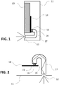
- Figure 1 illustrates a display device such as a flat television, shown in cross section.
- An enclosing cabinet 11 contains a display 13.
- This display may for example be an LCD display or an OLED display.
- the light sources 15 may be LEDs or other light sources. These light sources emit light that is intended to be radiated outside the cabinet of the television.
- a light source may include an LED that is used to indicate the power state of the device to the users. This LED may switch on or off, or change colour, to indicate that the television is in standby, or is starting up, or is operational.
- Another example of a light source is an infra-red LED that may send signals to other devices in order to control them.
- the detectors 16 may for example be photodiodes, or photoconductive devices. They serve to receive light signals that control the operation of the device.
- an infra-red detector may be used to receive infra-red signals emitted by a remote control operated by the user in order to control the device.
- a visible light detector may be used to measure the level of ambient light outside the device cabinet, so the brightness of the display 13 can be adjusted to the environment.
- an image sensor such as a CCD, that capture images used for video communication.
- the light emitted from the light sources 15 or to be detected by the detectors 16 has to travel through a hole or transparent section 12 located in the exterior of the enclosing cabinet 11 of the device.
- a light guide 17 is used to transport the light between the hole or transparent section 12 and the respective light sources 15 and detectors 16.
- This light guide has to be transparent for the wavelengths of light that is to travel through it, commonly visible light or infra-red light. Glass may be used or colorless plastics such as PMMA (polymethylmethacrylate).
- the light guide may consist of one or more pieces of solid material, fitted together. It may also consist of a bundle of optical fibers, possibly with optical coupling elements at the ends.
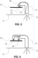
- FIG. 2 illustrates a basic shape of a light guide 17.
- the light guide consists of an elongated tube, in which light propagates through total internal reflection. This principle is well known from light guides used in LCD backlights for example.
- One end of the light guide is positioned over the interface components (15,16) mounted closely together on the circuit board 14.
- the other end of the light guide is positioned over the hole or transparent section 12 in the enclosing cabinet 11.
- Light emitted by a light source 15 enters the light guide at one end and exits the light guide at the other end, leaving the cabinet through the hole or transparent section 12.
- Light from outside the cabinet enters through the hole or transparent section 12, travels through the light guide and is detected by the detectors 16.
- Figure 3 illustrates another embodiment of the light guide.
- the light guide 17 is now equipped with a reflecting surface 18 placed under an angle, such that the light travelling through the light guide may be reflected towards the detectors 16 while the light guide itself is positioned essentially in parallel to the circuit board 14.
- light emitted from a light source 15 is reflected into the light guide 17 by the reflecting surface 18.
- the placement of the light guide in parallel to the circuit board saves space in the cabinet, which is beneficial in devices such as flat televisions, where it is desirable to keep the overall depth of the device to a minimum.
- the light guide is illustrated as a single part, but the end with the reflecting surface may well be added as a separate optical element.
- Figure 4 illustrates yet another embodiment of the light guide.
- the light guide 17 is forked at the end of the interface components (15,16), which enables these to be positioned more apart on the circuit board 14.
- the loss of light may be higher than in the above embodiments, but in many cases this may be affordable.
- a reflective surface under an angle may be used at the light guide's end closest to the cabinet hole.
- the forked ends of the light guide shown in Figure 4 may each be equipped with reflecting surfaces under an angle.
- Light signals traveling through the light guides for different purposes may interfere with each other or hamper each other's detection.
- An effective way of reducing such interference is the use of an optical filter over a detector to filter out any light not intended for that detector.
- a detector used to detect infra-red remote control signals may operate better when shielded from visible light.
- Figure 2 and Figure 3 both show an optical filter 19 positioned close to detector 16 in such a way that the filter blocks light from reaching the detector unintentionally. This only works if the interfering light signals have different properties, for example different wavelengths or polarization, so they can be separated by an optical filter.
- FIG. 5 illustrates how the two interfering light signals can be time multiplexed.
- the graph shows how a light source is alternatingly switched between an ON state and an OFF state, indicated by trace 21.
- a detector may be alternatingly switched between and OFF state and an ON state, indicated by trace 22.
- the synchronization is such that the light source is always OFF while the detector is ON, and vice versa.
- the switching is done sufficiently fast so as to not be visible to the human eye as flicker, typically at more than 100Hz.
- the off state of a detector as described above could mean literally that the detector is off. It can also mean that the detector is on, but that measurement results of the detector are not used during intervals in which the interfering light source is switched on.
- FIG. 6 illustrates how the above switching may be controlled.
- a controller 31 controls both light emission and light detection.
- the controller 31 switches an LED driver 33 on and off at the right moments. This results in light being emitted by an LED 35 at the right moments.
- the controller 31 sends on and off signals to a sample and hold circuit 32, which takes measurements from the detector 34. The synchronization is such that measurement values are only obtained while the LED is off, and the measure values are returned to the controller 31.
- Different control circuits could be devised, depending on the nature of the interface components, and on the integration with other functions of the device.
- Figure 7 shows a front view of a display device such as a television. This illustrates how the hole or transparent section 12 can be placed in the front side of the cabinet 11 that commonly surrounds the display 13 only as a narrow border or rim. The hole could of course be positioned in the top, bottom, left or right border of the cabinet, depending on the detailed design of the device.
Landscapes
- Physics & Mathematics (AREA)
- General Physics & Mathematics (AREA)
- Optics & Photonics (AREA)
- Devices For Indicating Variable Information By Combining Individual Elements (AREA)
- Details Of Television Systems (AREA)
- Optical Communication System (AREA)
- Selective Calling Equipment (AREA)
- Engineering & Computer Science (AREA)
- Multimedia (AREA)
- Signal Processing (AREA)
Description
- The present invention relates to electronic audio and video devices that emit and receive light signals, and in particular, but not exclusively, to display devices and televisions.
- Many electronic consumer devices emit and/or receive light signals during their operation for signaling and control purposes. For example, many DVD and Blu-ray players are controlled using an infrared light based remote control. They often contain LED indicators that serve, for example, to signal the standby status of the device to the user.
- In televisions these same functions of infrared remote control and status LEDs are commonly present. In addition a television is often equipped with a light sensor that measures the ambient illumination level in the environment so that the brightness of the television display may be adapted to the environment. More and different light signals may be received or emitted by other devices.
- The light received or emitted for signaling and control purposes commonly travels through holes in the front of the device's cabinet, or through parts of the cabinet that are optically transparent. The electronics related to the optical functions, such as LEDs, sensors and driving electronics are commonly placed on a printed circuit board placed behind these holes.
- In modern flat screen television there is a trend to minimize the cabinet size, leaving as much as possible only a narrow rim around the display as seen from the front. This conflicts with the need for the optical elements and related electronics mentioned above. A possible solution is to use a light guide to transport the light for the remote control as described in
US 5,036,188 A . This allows the infrared sensor and related electronics to be located behind the display instead of behind the optical hole in the cabinet. - Patent document
US2009/0237910 discloses a light indicator fixed to a front panel of an electronic device, such as an audio/video device, by means of an LED coupled to a light conducting lens. - It is an object of the invention to provide a low-cost solution for electronic audio and video devices to handle multiple light signals while requiring a limited amount of space in the enclosing cabinet of the device.
- For this purpose, according to a first aspect of the invention, an audio/video device comprises an enclosing cabinet and an electronic circuitry comprising at least two interface components, said circuitry being located within the cabinet capable of using at least two light signals, each associated with one of the interface components, and being received as a control signal or emitted as a feedback signal, where the audio/video device comprises a single light guide for transporting the light signals inside the cabinet between a hole or transparent part in the exterior of the enclosing cabinet and the respective interface components.
- These measures have the effect that in an audio/video device multiple detectors and light sources can be mounted on the main circuit board while being optically connected to the outside environment as their function requires. This saves the cost of an extra circuit board, while the additional cost introduced is limited to only a single light guide. Also it saves space in parts of the enclosing cabinet, which may be favorable to the design, for example in narrow-rimmed flat televisions.
- In an embodiment of the device at least one interface component comprises a light source for emitting a first one of the light signals and at least one interface component comprises a light detector for detection of a second one of the light signals, the device comprising a control circuit for activating the detector and light source in a time multiplexed mode to prevent interference between the detection and the emission.
- A further embodiment of the device comprises an optical filter for shielding at least one interface component, comprising a detector, from light not intended for said detector by filtering out optical wavelengths different from the optical wavelengths of the light signals that are intended for said detector.
- These and other aspects of the invention will be apparent from and elucidated further with reference to the embodiments described by way of example in the following description and with reference to the accompanying drawings, in which
-
Fig. 1 shows a display device with a circuit board, LEDs and detectors, a light guide and a hole in the device cabinet; -
Fig. 2 shows a circuit board with detectors and LEDs with a light guide; -
Fig. 3 shows a circuit board with detectors and LEDs with a light guide with a reflective surface; -
Fig. 4 shows a circuit board with detectors and LEDs with a forked light guide; -
Fig. 5 shows how a detector and an LED are alternatingly switched between ON and OFF states; -
Fig. 6 shows a circuit to control the switching of a detector and an LED; -
Fig. 7 shows a front view of a display device with a hole in a narrow cabinet border. - The following description focusses on embodiments of the invention applied in a flat television. However, it must be appreciated that the invention is not limited to televisions only but may be applied in other audio/video devices such as, for example, computer monitors, DVD players, Blu-ray Disk players or Home Theater Systems.
-
Figure 1 illustrates a display device such as a flat television, shown in cross section. An enclosingcabinet 11 contains adisplay 13. This display may for example be an LCD display or an OLED display. Behind the display, as seen from the front of the device, acircuit board 14 is located, containing the main electronic circuitry of the television. -
Light sources 15 anddetectors 16, together referred to as interface components, form part of this circuitry. Thelight sources 15 may be LEDs or other light sources. These light sources emit light that is intended to be radiated outside the cabinet of the television. For example, a light source may include an LED that is used to indicate the power state of the device to the users. This LED may switch on or off, or change colour, to indicate that the television is in standby, or is starting up, or is operational. Another example of a light source is an infra-red LED that may send signals to other devices in order to control them. - The
detectors 16 may for example be photodiodes, or photoconductive devices. They serve to receive light signals that control the operation of the device. For example, an infra-red detector may be used to receive infra-red signals emitted by a remote control operated by the user in order to control the device. As another example, a visible light detector may be used to measure the level of ambient light outside the device cabinet, so the brightness of thedisplay 13 can be adjusted to the environment. Yet another example is an image sensor such as a CCD, that capture images used for video communication. - The light emitted from the
light sources 15 or to be detected by thedetectors 16 has to travel through a hole ortransparent section 12 located in the exterior of the enclosingcabinet 11 of the device. To transport the light between the hole ortransparent section 12 and therespective light sources 15 anddetectors 16, alight guide 17 is used. This light guide has to be transparent for the wavelengths of light that is to travel through it, commonly visible light or infra-red light. Glass may be used or colorless plastics such as PMMA (polymethylmethacrylate). The light guide may consist of one or more pieces of solid material, fitted together. It may also consist of a bundle of optical fibers, possibly with optical coupling elements at the ends. -
Figure 2 illustrates a basic shape of alight guide 17. In this embodiment a simple single light guide is used. The light guide consists of an elongated tube, in which light propagates through total internal reflection. This principle is well known from light guides used in LCD backlights for example. One end of the light guide is positioned over the interface components (15,16) mounted closely together on thecircuit board 14. The other end of the light guide is positioned over the hole ortransparent section 12 in the enclosingcabinet 11. Light emitted by alight source 15 enters the light guide at one end and exits the light guide at the other end, leaving the cabinet through the hole ortransparent section 12. Light from outside the cabinet enters through the hole ortransparent section 12, travels through the light guide and is detected by thedetectors 16. -
Figure 3 illustrates another embodiment of the light guide. Thelight guide 17 is now equipped with a reflectingsurface 18 placed under an angle, such that the light travelling through the light guide may be reflected towards thedetectors 16 while the light guide itself is positioned essentially in parallel to thecircuit board 14. Similarly, light emitted from alight source 15 is reflected into thelight guide 17 by the reflectingsurface 18. The placement of the light guide in parallel to the circuit board saves space in the cabinet, which is beneficial in devices such as flat televisions, where it is desirable to keep the overall depth of the device to a minimum. InFigure 3 the light guide is illustrated as a single part, but the end with the reflecting surface may well be added as a separate optical element. -
Figure 4 illustrates yet another embodiment of the light guide. In this case thelight guide 17 is forked at the end of the interface components (15,16), which enables these to be positioned more apart on thecircuit board 14. In this embodiment the loss of light may be higher than in the above embodiments, but in many cases this may be affordable. - It is clear that many other embodiments of the light guide are possible, and that features of the embodiments presented here can be combined in different ways. For example, a reflective surface under an angle may be used at the light guide's end closest to the cabinet hole. As another example, the forked ends of the light guide shown in
Figure 4 may each be equipped with reflecting surfaces under an angle. - Light signals traveling through the light guides for different purposes may interfere with each other or hamper each other's detection. An effective way of reducing such interference is the use of an optical filter over a detector to filter out any light not intended for that detector. For example, a detector used to detect infra-red remote control signals may operate better when shielded from visible light.
Figure 2 andFigure 3 both show anoptical filter 19 positioned close todetector 16 in such a way that the filter blocks light from reaching the detector unintentionally. This only works if the interfering light signals have different properties, for example different wavelengths or polarization, so they can be separated by an optical filter. - If light signals interfere with each other that are of the same wavelength, they may be operated in a time multiplexed mode to avoid interference. For example, light emitted by a power indicator LED could hamper the correct measurement of ambient light levels.
Figure 5 illustrates how the two interfering light signals can be time multiplexed. The graph shows how a light source is alternatingly switched between an ON state and an OFF state, indicated bytrace 21. At the same time a detector may be alternatingly switched between and OFF state and an ON state, indicated bytrace 22. The synchronization is such that the light source is always OFF while the detector is ON, and vice versa. Thus the light emitted by the light source will not interfere with the detection of other light in the same region of wavelengths. The switching is done sufficiently fast so as to not be visible to the human eye as flicker, typically at more than 100Hz. - The off state of a detector as described above could mean literally that the detector is off. It can also mean that the detector is on, but that measurement results of the detector are not used during intervals in which the interfering light source is switched on.
-
Figure 6 illustrates how the above switching may be controlled. Acontroller 31 controls both light emission and light detection. To control light emission, thecontroller 31 switches anLED driver 33 on and off at the right moments. This results in light being emitted by anLED 35 at the right moments. To control the light detection, thecontroller 31 sends on and off signals to a sample and holdcircuit 32, which takes measurements from thedetector 34. The synchronization is such that measurement values are only obtained while the LED is off, and the measure values are returned to thecontroller 31. Different control circuits could be devised, depending on the nature of the interface components, and on the integration with other functions of the device. -
Figure 7 shows a front view of a display device such as a television. This illustrates how the hole ortransparent section 12 can be placed in the front side of thecabinet 11 that commonly surrounds thedisplay 13 only as a narrow border or rim. The hole could of course be positioned in the top, bottom, left or right border of the cabinet, depending on the detailed design of the device. - In non-display audio/video devices there is more freedom in choosing the location of the hole or transparent section in the enclosing cabinet. It will commonly be located in the front of the cabinet, which is most convenient for receiving remote control light signals, and for sending optical feedback signals to a user.
Claims (9)
- An audio/video device comprising an enclosing cabinet (11) and an electronic circuitry (14) comprising at least two interface components (15, 16), said circuitry being located within the cabinet capable of using at least two light signals, each associated with one of the interface components, and being received as a control signal formed by light irradiating the outside of the cabinet, or being emitted as a feedback signal to be radiated outside the cabinet, where the audio/video device comprises a single light guide (17) for transporting the light signals inside the cabinet between a hole or transparent part (12) in the exterior of the enclosing cabinet and the respective interface components.
- A device according to claim 1 where at least one interface component comprises a light source (15) for emitting a first one of the light signals and at least one interface component comprises a light detector (16) for detection of a second one of the light signals, the device comprising a control circuit (31) for activating the detector (34) and light source (35) in a time multiplexed mode to prevent interference between the detection and the emission.
- A device according to claim 2 comprising an optical filter (19) for shielding at least the interface component comprising the detector (16), from light not intended for said detector by filtering out optical wavelengths different from the optical wavelengths of the light signals that are intended for said detector.
- A device according to any of the previous claims where the device is a display device.
- A display device according to claim 4, where the display area is substantially enclosed with a narrow cabinet border, and the hole or transparent section (12) of the enclosing cabinet (11) is located within said border.
- A device according to claims 2 or 3 where the detector is arranged to detect light signals of a remote control device.
- A device according to claim 2 where the light source is arranged to emit light signals indicating a status of the device to a user.
- A device according to claims 2 or 3 where the detector is arranged to measure ambient light levels to control one or more functions of the device.
- A device according to claim 8 where the controlled functions include a display brightness.
Priority Applications (1)
| Application Number | Priority Date | Filing Date | Title |
|---|---|---|---|
| EP14708293.7A EP2965136B1 (en) | 2013-03-07 | 2014-03-07 | Electronic device with shared light guide |
Applications Claiming Priority (3)
| Application Number | Priority Date | Filing Date | Title |
|---|---|---|---|
| EP20130158158 EP2775333A1 (en) | 2013-03-07 | 2013-03-07 | Electronic device with shared light guide |
| PCT/EP2014/054446 WO2014135679A1 (en) | 2013-03-07 | 2014-03-07 | Electronic device with shared light guide |
| EP14708293.7A EP2965136B1 (en) | 2013-03-07 | 2014-03-07 | Electronic device with shared light guide |
Publications (2)
| Publication Number | Publication Date |
|---|---|
| EP2965136A1 EP2965136A1 (en) | 2016-01-13 |
| EP2965136B1 true EP2965136B1 (en) | 2017-01-25 |
Family
ID=47900665
Family Applications (2)
| Application Number | Title | Priority Date | Filing Date |
|---|---|---|---|
| EP20130158158 Withdrawn EP2775333A1 (en) | 2013-03-07 | 2013-03-07 | Electronic device with shared light guide |
| EP14708293.7A Not-in-force EP2965136B1 (en) | 2013-03-07 | 2014-03-07 | Electronic device with shared light guide |
Family Applications Before (1)
| Application Number | Title | Priority Date | Filing Date |
|---|---|---|---|
| EP20130158158 Withdrawn EP2775333A1 (en) | 2013-03-07 | 2013-03-07 | Electronic device with shared light guide |
Country Status (4)
| Country | Link |
|---|---|
| EP (2) | EP2775333A1 (en) |
| KR (1) | KR20150119488A (en) |
| CN (1) | CN105164561A (en) |
| WO (1) | WO2014135679A1 (en) |
Families Citing this family (3)
| Publication number | Priority date | Publication date | Assignee | Title |
|---|---|---|---|---|
| JP2020095061A (en) | 2016-03-08 | 2020-06-18 | パナソニック Avc ネットワークス クアラルンプール マレーシア スンディリアン ブルハドPanasonic Avc Networks Kuala Lumpur Malaysia Sdn. Bhd. | Video display device |
| FR3050541B1 (en) * | 2016-04-26 | 2019-07-12 | Valeo Comfort And Driving Assistance | DISPLAY |
| EP3642813B1 (en) | 2017-06-19 | 2021-06-02 | Signify Holding B.V. | A sensor assembly and a device comprising such sensor assembly |
Family Cites Families (6)
| Publication number | Priority date | Publication date | Assignee | Title |
|---|---|---|---|---|
| JPH0325121U (en) | 1989-07-24 | 1991-03-14 | ||
| KR970009824B1 (en) * | 1994-02-28 | 1997-06-18 | 현대전자산업 주식회사 | Barrel Photoreceptor Removal Device |
| US7452098B2 (en) * | 2001-06-15 | 2008-11-18 | Apple Inc. | Active enclosure for computing device |
| JP2007184191A (en) * | 2006-01-10 | 2007-07-19 | Funai Electric Co Ltd | Indicator device |
| JP4888429B2 (en) * | 2008-03-18 | 2012-02-29 | 株式会社Jvcケンウッド | Indicator device |
| US8651750B2 (en) * | 2009-11-19 | 2014-02-18 | Apple Inc. | Audio connectors with optical structures and electrical contacts |
-
2013
- 2013-03-07 EP EP20130158158 patent/EP2775333A1/en not_active Withdrawn
-
2014
- 2014-03-07 EP EP14708293.7A patent/EP2965136B1/en not_active Not-in-force
- 2014-03-07 KR KR1020157027780A patent/KR20150119488A/en not_active Ceased
- 2014-03-07 WO PCT/EP2014/054446 patent/WO2014135679A1/en not_active Ceased
- 2014-03-07 CN CN201480025119.2A patent/CN105164561A/en active Pending
Non-Patent Citations (1)
| Title |
|---|
| None * |
Also Published As
| Publication number | Publication date |
|---|---|
| EP2775333A1 (en) | 2014-09-10 |
| EP2965136A1 (en) | 2016-01-13 |
| KR20150119488A (en) | 2015-10-23 |
| CN105164561A (en) | 2015-12-16 |
| WO2014135679A1 (en) | 2014-09-12 |
Similar Documents
| Publication | Publication Date | Title |
|---|---|---|
| KR101573490B1 (en) | Light Signal Transmitting and Receiving Apparatus using Light Guide | |
| CN101042499B (en) | Liquid crystal display apparatus and backlight unit used in liquid crystal display apparatus | |
| US20190004668A1 (en) | Display device | |
| US20080283770A1 (en) | Illumination light detecting optical system and optical apparatus and endoscope apparatus provided with the same | |
| TWI352848B (en) | Optical display device | |
| JP2009032005A (en) | Input display device and input display panel | |
| EP2829794A1 (en) | Solid illumination device | |
| KR20080044017A (en) | touch screen | |
| US10712775B2 (en) | Dichroic combiner backlight used in a head mounted display | |
| WO2020059420A1 (en) | Light-source driving device and light emission device | |
| EP2775333A1 (en) | Electronic device with shared light guide | |
| JP2010231503A (en) | Position detecting device and electro-optical device | |
| US8013949B2 (en) | Liquid crystal display device with optoelectronic component and method for controlling backlighting of such a display device | |
| WO2017155000A1 (en) | Image display device | |
| US8217354B2 (en) | Remote sensing system and electronic apparatus having same | |
| US20140263973A1 (en) | Integrated module having multiple light emitters or sensors for televisions and other appliances | |
| JP6581670B2 (en) | Light curing device | |
| KR102211153B1 (en) | Camera module type sensor apparatus and camera module | |
| US20140184986A1 (en) | Display device | |
| US20170319055A1 (en) | Endoscopic illumination system | |
| JP2008298834A (en) | Liquid crystal display | |
| JPH1137930A (en) | Spectrophotometer | |
| JP4947080B2 (en) | Position detecting device and electro-optical device | |
| KR20200028385A (en) | Display device with integrated, optically operated proximity sensor system | |
| US9000355B2 (en) | Optical sensor |
Legal Events
| Date | Code | Title | Description |
|---|---|---|---|
| PUAI | Public reference made under article 153(3) epc to a published international application that has entered the european phase |
Free format text: ORIGINAL CODE: 0009012 |
|
| 17P | Request for examination filed |
Effective date: 20150928 |
|
| AK | Designated contracting states |
Kind code of ref document: A1 Designated state(s): AL AT BE BG CH CY CZ DE DK EE ES FI FR GB GR HR HU IE IS IT LI LT LU LV MC MK MT NL NO PL PT RO RS SE SI SK SM TR |
|
| AX | Request for extension of the european patent |
Extension state: BA ME |
|
| DAX | Request for extension of the european patent (deleted) | ||
| GRAP | Despatch of communication of intention to grant a patent |
Free format text: ORIGINAL CODE: EPIDOSNIGR1 |
|
| RIC1 | Information provided on ipc code assigned before grant |
Ipc: H04N 5/64 20060101ALI20160701BHEP Ipc: G02B 6/42 20060101AFI20160701BHEP Ipc: G08C 23/04 20060101ALI20160701BHEP |
|
| INTG | Intention to grant announced |
Effective date: 20160803 |
|
| GRAS | Grant fee paid |
Free format text: ORIGINAL CODE: EPIDOSNIGR3 |
|
| GRAA | (expected) grant |
Free format text: ORIGINAL CODE: 0009210 |
|
| AK | Designated contracting states |
Kind code of ref document: B1 Designated state(s): AL AT BE BG CH CY CZ DE DK EE ES FI FR GB GR HR HU IE IS IT LI LT LU LV MC MK MT NL NO PL PT RO RS SE SI SK SM TR |
|
| REG | Reference to a national code |
Ref country code: GB Ref legal event code: FG4D |
|
| REG | Reference to a national code |
Ref country code: CH Ref legal event code: EP |
|
| REG | Reference to a national code |
Ref country code: AT Ref legal event code: REF Ref document number: 864463 Country of ref document: AT Kind code of ref document: T Effective date: 20170215 |
|
| REG | Reference to a national code |
Ref country code: FR Ref legal event code: PLFP Year of fee payment: 4 |
|
| REG | Reference to a national code |
Ref country code: IE Ref legal event code: FG4D |
|
| REG | Reference to a national code |
Ref country code: DE Ref legal event code: R096 Ref document number: 602014006363 Country of ref document: DE |
|
| REG | Reference to a national code |
Ref country code: LT Ref legal event code: MG4D |
|
| REG | Reference to a national code |
Ref country code: NL Ref legal event code: MP Effective date: 20170125 |
|
| REG | Reference to a national code |
Ref country code: AT Ref legal event code: MK05 Ref document number: 864463 Country of ref document: AT Kind code of ref document: T Effective date: 20170125 |
|
| PG25 | Lapsed in a contracting state [announced via postgrant information from national office to epo] |
Ref country code: NL Free format text: LAPSE BECAUSE OF FAILURE TO SUBMIT A TRANSLATION OF THE DESCRIPTION OR TO PAY THE FEE WITHIN THE PRESCRIBED TIME-LIMIT Effective date: 20170125 |
|
| PG25 | Lapsed in a contracting state [announced via postgrant information from national office to epo] |
Ref country code: FI Free format text: LAPSE BECAUSE OF FAILURE TO SUBMIT A TRANSLATION OF THE DESCRIPTION OR TO PAY THE FEE WITHIN THE PRESCRIBED TIME-LIMIT Effective date: 20170125 Ref country code: NO Free format text: LAPSE BECAUSE OF FAILURE TO SUBMIT A TRANSLATION OF THE DESCRIPTION OR TO PAY THE FEE WITHIN THE PRESCRIBED TIME-LIMIT Effective date: 20170425 Ref country code: GR Free format text: LAPSE BECAUSE OF FAILURE TO SUBMIT A TRANSLATION OF THE DESCRIPTION OR TO PAY THE FEE WITHIN THE PRESCRIBED TIME-LIMIT Effective date: 20170426 Ref country code: HR Free format text: LAPSE BECAUSE OF FAILURE TO SUBMIT A TRANSLATION OF THE DESCRIPTION OR TO PAY THE FEE WITHIN THE PRESCRIBED TIME-LIMIT Effective date: 20170125 Ref country code: LT Free format text: LAPSE BECAUSE OF FAILURE TO SUBMIT A TRANSLATION OF THE DESCRIPTION OR TO PAY THE FEE WITHIN THE PRESCRIBED TIME-LIMIT Effective date: 20170125 Ref country code: IS Free format text: LAPSE BECAUSE OF FAILURE TO SUBMIT A TRANSLATION OF THE DESCRIPTION OR TO PAY THE FEE WITHIN THE PRESCRIBED TIME-LIMIT Effective date: 20170525 |
|
| PG25 | Lapsed in a contracting state [announced via postgrant information from national office to epo] |
Ref country code: ES Free format text: LAPSE BECAUSE OF FAILURE TO SUBMIT A TRANSLATION OF THE DESCRIPTION OR TO PAY THE FEE WITHIN THE PRESCRIBED TIME-LIMIT Effective date: 20170125 Ref country code: AT Free format text: LAPSE BECAUSE OF FAILURE TO SUBMIT A TRANSLATION OF THE DESCRIPTION OR TO PAY THE FEE WITHIN THE PRESCRIBED TIME-LIMIT Effective date: 20170125 Ref country code: LV Free format text: LAPSE BECAUSE OF FAILURE TO SUBMIT A TRANSLATION OF THE DESCRIPTION OR TO PAY THE FEE WITHIN THE PRESCRIBED TIME-LIMIT Effective date: 20170125 Ref country code: SE Free format text: LAPSE BECAUSE OF FAILURE TO SUBMIT A TRANSLATION OF THE DESCRIPTION OR TO PAY THE FEE WITHIN THE PRESCRIBED TIME-LIMIT Effective date: 20170125 Ref country code: BG Free format text: LAPSE BECAUSE OF FAILURE TO SUBMIT A TRANSLATION OF THE DESCRIPTION OR TO PAY THE FEE WITHIN THE PRESCRIBED TIME-LIMIT Effective date: 20170425 Ref country code: PT Free format text: LAPSE BECAUSE OF FAILURE TO SUBMIT A TRANSLATION OF THE DESCRIPTION OR TO PAY THE FEE WITHIN THE PRESCRIBED TIME-LIMIT Effective date: 20170525 Ref country code: PL Free format text: LAPSE BECAUSE OF FAILURE TO SUBMIT A TRANSLATION OF THE DESCRIPTION OR TO PAY THE FEE WITHIN THE PRESCRIBED TIME-LIMIT Effective date: 20170125 Ref country code: RS Free format text: LAPSE BECAUSE OF FAILURE TO SUBMIT A TRANSLATION OF THE DESCRIPTION OR TO PAY THE FEE WITHIN THE PRESCRIBED TIME-LIMIT Effective date: 20170125 |
|
| REG | Reference to a national code |
Ref country code: DE Ref legal event code: R097 Ref document number: 602014006363 Country of ref document: DE |
|
| PG25 | Lapsed in a contracting state [announced via postgrant information from national office to epo] |
Ref country code: SK Free format text: LAPSE BECAUSE OF FAILURE TO SUBMIT A TRANSLATION OF THE DESCRIPTION OR TO PAY THE FEE WITHIN THE PRESCRIBED TIME-LIMIT Effective date: 20170125 Ref country code: EE Free format text: LAPSE BECAUSE OF FAILURE TO SUBMIT A TRANSLATION OF THE DESCRIPTION OR TO PAY THE FEE WITHIN THE PRESCRIBED TIME-LIMIT Effective date: 20170125 Ref country code: RO Free format text: LAPSE BECAUSE OF FAILURE TO SUBMIT A TRANSLATION OF THE DESCRIPTION OR TO PAY THE FEE WITHIN THE PRESCRIBED TIME-LIMIT Effective date: 20170125 Ref country code: CZ Free format text: LAPSE BECAUSE OF FAILURE TO SUBMIT A TRANSLATION OF THE DESCRIPTION OR TO PAY THE FEE WITHIN THE PRESCRIBED TIME-LIMIT Effective date: 20170125 |
|
| REG | Reference to a national code |
Ref country code: CH Ref legal event code: PL |
|
| PG25 | Lapsed in a contracting state [announced via postgrant information from national office to epo] |
Ref country code: SM Free format text: LAPSE BECAUSE OF FAILURE TO SUBMIT A TRANSLATION OF THE DESCRIPTION OR TO PAY THE FEE WITHIN THE PRESCRIBED TIME-LIMIT Effective date: 20170125 Ref country code: DK Free format text: LAPSE BECAUSE OF FAILURE TO SUBMIT A TRANSLATION OF THE DESCRIPTION OR TO PAY THE FEE WITHIN THE PRESCRIBED TIME-LIMIT Effective date: 20170125 Ref country code: MC Free format text: LAPSE BECAUSE OF FAILURE TO SUBMIT A TRANSLATION OF THE DESCRIPTION OR TO PAY THE FEE WITHIN THE PRESCRIBED TIME-LIMIT Effective date: 20170125 |
|
| PLBE | No opposition filed within time limit |
Free format text: ORIGINAL CODE: 0009261 |
|
| STAA | Information on the status of an ep patent application or granted ep patent |
Free format text: STATUS: NO OPPOSITION FILED WITHIN TIME LIMIT |
|
| REG | Reference to a national code |
Ref country code: IE Ref legal event code: MM4A |
|
| 26N | No opposition filed |
Effective date: 20171026 |
|
| PG25 | Lapsed in a contracting state [announced via postgrant information from national office to epo] |
Ref country code: LU Free format text: LAPSE BECAUSE OF NON-PAYMENT OF DUE FEES Effective date: 20170307 |
|
| REG | Reference to a national code |
Ref country code: FR Ref legal event code: PLFP Year of fee payment: 5 |
|
| PG25 | Lapsed in a contracting state [announced via postgrant information from national office to epo] |
Ref country code: SI Free format text: LAPSE BECAUSE OF FAILURE TO SUBMIT A TRANSLATION OF THE DESCRIPTION OR TO PAY THE FEE WITHIN THE PRESCRIBED TIME-LIMIT Effective date: 20170125 Ref country code: CH Free format text: LAPSE BECAUSE OF NON-PAYMENT OF DUE FEES Effective date: 20170331 Ref country code: IE Free format text: LAPSE BECAUSE OF NON-PAYMENT OF DUE FEES Effective date: 20170307 Ref country code: LI Free format text: LAPSE BECAUSE OF NON-PAYMENT OF DUE FEES Effective date: 20170331 |
|
| REG | Reference to a national code |
Ref country code: BE Ref legal event code: MM Effective date: 20170331 |
|
| PG25 | Lapsed in a contracting state [announced via postgrant information from national office to epo] |
Ref country code: BE Free format text: LAPSE BECAUSE OF NON-PAYMENT OF DUE FEES Effective date: 20170331 |
|
| PG25 | Lapsed in a contracting state [announced via postgrant information from national office to epo] |
Ref country code: MT Free format text: LAPSE BECAUSE OF NON-PAYMENT OF DUE FEES Effective date: 20170307 |
|
| GBPC | Gb: european patent ceased through non-payment of renewal fee |
Effective date: 20180307 |
|
| PG25 | Lapsed in a contracting state [announced via postgrant information from national office to epo] |
Ref country code: GB Free format text: LAPSE BECAUSE OF NON-PAYMENT OF DUE FEES Effective date: 20180307 |
|
| PGFP | Annual fee paid to national office [announced via postgrant information from national office to epo] |
Ref country code: IT Payment date: 20190321 Year of fee payment: 6 Ref country code: DE Payment date: 20190225 Year of fee payment: 6 |
|
| PGFP | Annual fee paid to national office [announced via postgrant information from national office to epo] |
Ref country code: FR Payment date: 20190220 Year of fee payment: 6 |
|
| PG25 | Lapsed in a contracting state [announced via postgrant information from national office to epo] |
Ref country code: HU Free format text: LAPSE BECAUSE OF FAILURE TO SUBMIT A TRANSLATION OF THE DESCRIPTION OR TO PAY THE FEE WITHIN THE PRESCRIBED TIME-LIMIT; INVALID AB INITIO Effective date: 20140307 |
|
| PG25 | Lapsed in a contracting state [announced via postgrant information from national office to epo] |
Ref country code: CY Free format text: LAPSE BECAUSE OF FAILURE TO SUBMIT A TRANSLATION OF THE DESCRIPTION OR TO PAY THE FEE WITHIN THE PRESCRIBED TIME-LIMIT Effective date: 20170125 |
|
| PG25 | Lapsed in a contracting state [announced via postgrant information from national office to epo] |
Ref country code: MK Free format text: LAPSE BECAUSE OF FAILURE TO SUBMIT A TRANSLATION OF THE DESCRIPTION OR TO PAY THE FEE WITHIN THE PRESCRIBED TIME-LIMIT Effective date: 20170125 |
|
| PG25 | Lapsed in a contracting state [announced via postgrant information from national office to epo] |
Ref country code: TR Free format text: LAPSE BECAUSE OF FAILURE TO SUBMIT A TRANSLATION OF THE DESCRIPTION OR TO PAY THE FEE WITHIN THE PRESCRIBED TIME-LIMIT Effective date: 20170125 |
|
| PG25 | Lapsed in a contracting state [announced via postgrant information from national office to epo] |
Ref country code: AL Free format text: LAPSE BECAUSE OF FAILURE TO SUBMIT A TRANSLATION OF THE DESCRIPTION OR TO PAY THE FEE WITHIN THE PRESCRIBED TIME-LIMIT Effective date: 20170125 |
|
| REG | Reference to a national code |
Ref country code: DE Ref legal event code: R119 Ref document number: 602014006363 Country of ref document: DE |
|
| PG25 | Lapsed in a contracting state [announced via postgrant information from national office to epo] |
Ref country code: FR Free format text: LAPSE BECAUSE OF NON-PAYMENT OF DUE FEES Effective date: 20200331 Ref country code: DE Free format text: LAPSE BECAUSE OF NON-PAYMENT OF DUE FEES Effective date: 20201001 |
|
| PG25 | Lapsed in a contracting state [announced via postgrant information from national office to epo] |
Ref country code: IT Free format text: LAPSE BECAUSE OF NON-PAYMENT OF DUE FEES Effective date: 20200307 |