EP2965054B1 - Superconducting thermal detector of terahertz radiation - Google Patents
Superconducting thermal detector of terahertz radiation Download PDFInfo
- Publication number
- EP2965054B1 EP2965054B1 EP14719807.1A EP14719807A EP2965054B1 EP 2965054 B1 EP2965054 B1 EP 2965054B1 EP 14719807 A EP14719807 A EP 14719807A EP 2965054 B1 EP2965054 B1 EP 2965054B1
- Authority
- EP
- European Patent Office
- Prior art keywords
- superconducting
- bolometer
- thz
- inductance
- thermal
- Prior art date
- Legal status (The legal status is an assumption and is not a legal conclusion. Google has not performed a legal analysis and makes no representation as to the accuracy of the status listed.)
- Active
Links
Images

Classifications
-
- G—PHYSICS
- G01—MEASURING; TESTING
- G01J—MEASUREMENT OF INTENSITY, VELOCITY, SPECTRAL CONTENT, POLARISATION, PHASE OR PULSE CHARACTERISTICS OF INFRARED, VISIBLE OR ULTRAVIOLET LIGHT; COLORIMETRY; RADIATION PYROMETRY
- G01J5/00—Radiation pyrometry, e.g. infrared or optical thermometry
- G01J5/10—Radiation pyrometry, e.g. infrared or optical thermometry using electric radiation detectors
- G01J5/20—Radiation pyrometry, e.g. infrared or optical thermometry using electric radiation detectors using resistors, thermistors or semiconductors sensitive to radiation, e.g. photoconductive devices
-
- G—PHYSICS
- G01—MEASURING; TESTING
- G01J—MEASUREMENT OF INTENSITY, VELOCITY, SPECTRAL CONTENT, POLARISATION, PHASE OR PULSE CHARACTERISTICS OF INFRARED, VISIBLE OR ULTRAVIOLET LIGHT; COLORIMETRY; RADIATION PYROMETRY
- G01J5/00—Radiation pyrometry, e.g. infrared or optical thermometry
- G01J5/02—Constructional details
- G01J5/0225—Shape of the cavity itself or of elements contained in or suspended over the cavity
- G01J5/024—Special manufacturing steps or sacrificial layers or layer structures
-
- H—ELECTRICITY
- H10—SEMICONDUCTOR DEVICES; ELECTRIC SOLID-STATE DEVICES NOT OTHERWISE PROVIDED FOR
- H10N—ELECTRIC SOLID-STATE DEVICES NOT OTHERWISE PROVIDED FOR
- H10N15/00—Thermoelectric devices without a junction of dissimilar materials; Thermomagnetic devices, e.g. using the Nernst-Ettingshausen effect
-
- G—PHYSICS
- G01—MEASURING; TESTING
- G01J—MEASUREMENT OF INTENSITY, VELOCITY, SPECTRAL CONTENT, POLARISATION, PHASE OR PULSE CHARACTERISTICS OF INFRARED, VISIBLE OR ULTRAVIOLET LIGHT; COLORIMETRY; RADIATION PYROMETRY
- G01J5/00—Radiation pyrometry, e.g. infrared or optical thermometry
- G01J5/10—Radiation pyrometry, e.g. infrared or optical thermometry using electric radiation detectors
- G01J2005/106—Arrays
-
- G—PHYSICS
- G01—MEASURING; TESTING
- G01J—MEASUREMENT OF INTENSITY, VELOCITY, SPECTRAL CONTENT, POLARISATION, PHASE OR PULSE CHARACTERISTICS OF INFRARED, VISIBLE OR ULTRAVIOLET LIGHT; COLORIMETRY; RADIATION PYROMETRY
- G01J5/00—Radiation pyrometry, e.g. infrared or optical thermometry
- G01J5/10—Radiation pyrometry, e.g. infrared or optical thermometry using electric radiation detectors
- G01J5/20—Radiation pyrometry, e.g. infrared or optical thermometry using electric radiation detectors using resistors, thermistors or semiconductors sensitive to radiation, e.g. photoconductive devices
- G01J2005/208—Radiation pyrometry, e.g. infrared or optical thermometry using electric radiation detectors using resistors, thermistors or semiconductors sensitive to radiation, e.g. photoconductive devices superconductive
Definitions
- the present invention relates to a superconducting thermal detector according to Claim 1.
- the disclosure relates also to design, fabrication, readout techniques of a superconducting thermal detector and design and methods of microwave multiplexed read-out of the arrays of superconducting thermal detectors.
- the present disclosure relates also to a detector which detects electromagnetic waves at Terahertz (THz) frequencies, and more particularly to a superconducting bolometer type Terahertz wave detector.
- THz Terahertz
- Thermal detectors have been first introduced by S. P. Langley back in 1880.
- the operating principle of the bolometer is based on detection a small temperature change with a sensitive thermometer, whereby the said temperature change is caused due to a heat into which the absorbed radiation is transformed in the bolometer absorbing element ( Fig. 1 ).
- the thermometer is isolated from the thermal reservoir through a thermal link with a thermal conductance G .
- Thermal detectors with superconducting materials TES's
- TES's transition edge sensors
- the device based on utilizing said sensor to receive said temperature indicative output (claim 7); the device utilizing said sensor used as a variable inductance for electronic circuit means (claim 13); the device with electronic circuit means including oscillation means providing an output frequency varying due to temperature dependent inductance, whereby the output frequency of said oscillations means is temperature dependent (claim 14); the device of claim 1 including means for connecting said sensor with monitoring means capable of monitoring at least one of power and radiation whereby said device produces a temperature-indicative output that is indicative of at least one of power and radiation monitored by said monitor means (claim 15); superconductor-based detection devices comprising absorbing elements of at least one of power and radiation (claims 19 - 25).
- microwave kinetic inductance detectors opened possibility to build multipixel superconducting THz imaging arrays with hundreds of pixel readout out only with a single pair of coaxial lines. Below in the text we give a brief overview of these detectors.
- the demonstrated by P.K. Day et al KID detector represents a superconducting quarterwavelength transmission line resonator made out of 220 nm thick aluminium film.
- the readout method of KID is based on microwave measurement of the complex impedance of a thin superconducting film.
- Its equivalent circuit represents a LC resonant circuit which is capacitively coupled to a transmission line.
- the resonant circuit consists of a capacitance and an alternated by the incident radiation inductance.
- the microwave current distribution is nonuniform in a KID device: it is mainly sensitive to the photon absorption in the centre of a superconducting strip, with maximal optical response at the shorted end of the quarterwavelength resonator (and having zero response at the coupling end) [P.K. Day].
- the optical absorber has to be coupled to the resonator's shorted end.
- resonator-bolometer is an interesting option when quasiparticle recombination is too rapid, e.g., at higher temperatures.
- the thermally suspended island provides an opportunity to spread the absorbed photon energy uniformly across the inductor, which maximizes responsivity.
- the quasiparticle noise may be greatly reduced.
- the noise performance of available transistor amplifiers is considerably better than is needed to reach the fundamental sensitivity limits for bolometers (e.g., photon or phonon noise)."
- Imaging in the submillirnetre-wave to THz spectral regions of the electromagnetic spectrum has attracted a lot of interest for various applications.
- cameras operating in this wavelength range can be used for mapping the Cosmic Microwave Background, interstellar gas clouds, protoplanetary disks;
- imagery in the spectral range can be used for accurate mapping of atmospheric water vapour which is of great relevance to e.g. the greenhouse effect and also cloud formation, rainfall prediction and agriculture.
- terrestrial applications the most notable so far has been the imaging of concealed items under clothing, for instance hidden weapons, explosives, drugs and other contraband.
- This application benefits from i) the relative good penetration of the radiation in the said wavelength range and ii) the wavelengths in general which are short enough that image forming instruments can be developed which possess an aperture diameter less than one meter.
- Planck black body emission formula indicates the signal power at 94 GHz corresponding to a 1 K level of sensitivity at an ambient temperature of 300 K is ⁇ 260 fW (in single mode, 20 % relative bandwidth). Compare this with the single-mode power available in the LWIR (8 - 12 ⁇ m) of ⁇ 30 pW, i.e. some 2 orders of magnitude more signal power is present in the thermal infrared.
- Another push present both in passive and active systems is the desire to operate at higher frequencies: The angular resolution of an imaging system in proportional to the ratio of the operating wavelength to the diameter of the aperture, ⁇ / D ap .
- the primary detector architectures employed at present for terrestrial passive THz imaging are a) Heterodyne down conversion receivers, b) pre-amplified direct detection receivers, or c) unamplified direct detection receivers.
- a) and c) can in principle operate up to several THz, whilst b) is limited by the poor availability of Low Noise Amplifiers (LNAs) above 300 GHz.
- LNAs Low Noise Amplifiers
- Cost is a major issue for a) and b), while c) can be cheaper it tends to lag behind in sensitivity (at least if operated at room temperature).
- Recent developments are focused on pushing the LNA technology deep into the submm-wave range, but it may take some time before novel submmw LNAs become affordable.
- Packaging and assembly of MMIC's plays a major role here, not to mention device testing costs.
- cryogenic imaging systems In passive imaging mode, the simultaneous requirements for sensitivity, large pixel count, large FoV and operation in the submm-wave range has motivated the development of cryogenic imaging systems. With cooling it is possible to substantially increase the sensitivity of bolometers to the point where they outperform any room temperature (even pre-amplified) detector technology. While the introduction of a closed-cycle cooling adds cost, weight, power draw and footprint to the camera back-end, the front-end is in fact less complicated than with e.g. heterodyne or preamplified direct detection architectures. Cooled systems also can leverage from the rapid development of compact cryocoolers which are now in widespread use in medical MRI machines.
- cryogenic passive THz video-rate imager is the system demonstrator developed by VTT in 2010-2012.
- the system employs a linear array (128) of cryogenic antennacoupled hot-spot micro bolometers, each one of which is connected to a dedicated feedback preamplifier circuit.
- a 2D image is formed through the use of a conical scanning optical element which essentially causes the projection of each detector at the target plane to rotate a circle.
- a linear array of 128 detectors then draw 128 circles each slightly offset from each other in the vertical dimension.
- An image is generated through a software routine which interpolates the data points from the scan space to Cartesian space.
- a passive imager would greatly benefit from a 2D focal plane array (FPA):
- FPA focal plane array
- N ip N ip / N det scan positions for each frame.
- An application typically dictates a required frame-rate f frame .
- t int 1/( n f frame )
- the signal-to-noise ratio of a detector is proportional to t int (assuming white noise).
- the total parasitic conductive heat load to a 2D array with N det detectors is N det / 2 L 0 T h 2 ⁇ T c 2 / R , which is typically much more than the cooling overhead supplied by the cryocooler.
- the invention is intended to eliminate the defects of the prior art described above and for this purpose create an entirely new type of superconducting thermal detector.
- the object of the invention is a detector and readout method which allows for the construction of large format FPAs for the THz range that operate at temperatures that are readily accessible with 2-stage closed cycle cryocoolers. Similar detector arrays have been constructed for deep-cryogenic operation (T ⁇ 300 mK) (NIKA [8], MAKO [8], MUSICA [10], [11]) for astrophysical applications, but due to the prohibitive cost and complexity of the associated cryogenics such systems are unusable for most terrestrial (security) applications.
- the invention is based on a superconducting thermal detector (bolometer) where the thermometry is carried out by sensing the change in the amplitude or phase of a resonator circuit, consisting of a capacitor and a superconducting inductor where the said inductor is thermally isolated from the heat bath of the system (from the chip substrate).
- a superconducting thermal detector bolometer
- the bolometer according to the invention is defined by the features of Claim 1.
- the superconducting thermal detector (bolometer) in accordance with the invention operates in a temperature range from 1 Kelvin to 10 Kelvin enabling much cheaper infrastructure than the deep-cryogenic devices.
- the performance of the present invention is superior to the passive (non-cryogenic) THz detectors.
- This invention provides a superconducting thermal detector (bolometer) to detect THz (0.1-1 THz bandwidth) radiation.
- the temperature sensitive superconducting meander is thermally isolated from the thermal bath by micro-suspensions.
- superconducting THz superconducting thermal detector (bolometer) and arrays of these detectors are to be used as THz radiation sensing elements (detectors) in cryogenic THz radiation passive cameras operating in two-stage cryocooling systems.
- the detector and readout system are based on a fundamental property of superconductors: kinetic inductance. Arising from the inertia of the superconducting charge carriers (Cooper pairs), superconductors exhibit inductance in excess of the geometric inductance associated with normal metals. Also normal metals do exhibit kinetic inductance, but the wavelengths where kinetic inductance in normal metals becomes relevant lies in the IR and optical wavelengths, whereas in superconductors the relevant frequency scale is in the THz region.
- kinetic inductance Arising from the inertia of the superconducting charge carriers (Cooper pairs), superconductors exhibit inductance in excess of the geometric inductance associated with normal metals. Also normal metals do exhibit kinetic inductance, but the wavelengths where kinetic inductance in normal metals becomes relevant lies in the IR and optical wavelengths, whereas in superconductors the relevant frequency scale is in the THz region.
- L k L k (0)/(1 - ( T / T C ) 4 ), where T C is the transition temperature of a superconductor, L k 0 ⁇ ⁇ 0 ⁇ L 0 2 l / wd for a narrow thin superconducting strip, with magnetic penetration depth ⁇ L 0 2 , having a geometry of length l , width w and thickness d.
- a kinetic inductor can be used as a thermometer to sense its physical temperature. The temperature dependent kinetic inductance is associated with the excess quasiparticle density present within the superconductor.
- the excess quasiparticles can be generated by either incident photons (with energy greater than twice the superconducting energy gap) or through thermal excitation. In the former case the phenomenon is commonly referred to as “non-equilibrium kinetic inductance”, whereas the latter is “equilibrium kinetic inductance”.
- the superconducting thermal detector is thermally isolated from the bath enabling its efficient operation in an equilibrium regime, meaning that the incident THz radiation is absorbed by the electrons of a superconductor which are in a thermal equilibrium with its phonons at temperature T .
- Typical temperature operation regime of such a detector lies between ⁇ 0.3 T C and T C .
- the noise equivalent power background-limited performance NEP BLIP for the detector at 350 GHz is about ⁇ 10 -15 W/Hz 1/2 for a single mode assuming quantum efficiency of unity for the 300 K black-body object emitting radiation in a 100 GHz bandwidth.
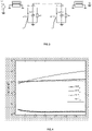
- the NEP contributions with dissipative readout for a superconducting thermal detector (bolometer) are plotted in FIG. 4 with detector parameters as explained in the description of FIG. 4 .
- the superconducting meander line with temperature dependent inductance L ( T ) is connected to the shunting capacitor C sh to form a resonant tank circuit, which is in turn coupled to the readout superconducting transmission line through the coupling capacitor C c ( Fig. 3 ).
- the detector responsivity then yields dV / dP ⁇ 10 5 V/W.
- a low noise amplifier is used to readout bolometer signal.
- the multiplexed arrays of superconducting thermal detectors represent a 2D matrix of resonant tank circuits (pixels) with alternated values of shunting capacitances in each of the resonant tank circuit (in each pixel), so that each resonant frequency is in one-toone correspondence to a single pixel.
- the pixels are capacitively coupled to a superconducting transmission line for a multiplexed microwave readout of a 2D bolometer pixel array.
- the optimal geometry design of the said bolometer arrays is implemented to eliminate electrical cross-talk between the pixels.
- a superconducting thermal detector comprises the micro- structure consisting of the following parts:
- the superconducting thermal detectors (bolometers) and arrays of those have been successfully fabricated and tested.
- FIG. 6 The measured temperature dependence of the resonant frequency is shown in FIG. 6 .
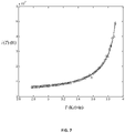
- FIG. 7 we show temperature dependence of kinetic inductance the deduced from data in FIG. 6 (circles).
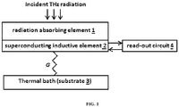
- Figure 1 shows general principle scheme of THz radiation detection with a superconducting thermal detector using the superconducting inductance.
- the incoming radiation is absorbed by the absorbing element 1 which is in a tight thermal contact with a superconducting inductor 2.
- the superconducting inductor is thermally isolated from the thermal bath (substrate) by micro-suspension legs, whose total thermal conductance is denoted by G.
- the signal is detected by the read-out circuit 4.
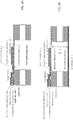
- Figure 2A shows a schematic cross-section of multi-layer structure of a superconducting thermal detector (bolometer).
- the detector is micro-machined using standard thin film deposition and micro-lithography methods.
- the substrate 3 represents a silicon wafer. Deposited thin films on top of the silicon substrate are: 1 st layer is a silicon etch-stop layer (optional in the process), 2 nd layer is a membrane layer 5, 3 rd layer is a superconducting inductor layer 2 and 1 st , 4 th layer is an insulating layer (dielectric) 7, 5 th layer is a superconducting layer 8 (optional in the process).
- the perforations 21 (optional in the process) in the membrane layer 5 are applied to form narrow micro-suspension legs for thermal insulation.
- the deep silicon etch through the substrate 3 is applied to form resonant optical ⁇ /4 cavity 9.
- Figure 2B shows the superconducting thermal detector (bolometer) as in FIG. 1 with an etched resonant optical ⁇ /4 cavity 9 and a back reflector 10 to enhance optical absorptivity.
- FIG. 3 shows an equivalent electrical circuit of an array of N superconducting thermal detectors (bolometers) capacitively coupled to a superconducting transmission line.
- Each pixel represents an inductance Li(T) embedded into a resonant circuit with the shunting capacitor Csh_i, where "i" denotes the number of the i th bolometer pixel.
- the microwave losses of each inductor are depicted with resistor R.
- the quality factor of the resonators is about 300.
- Figure 6 shows measured temperature dependence of the lowest frequency resonance in the 8-pixel array of superconducting thermal detectors (bolometers).
- Figure 7 shows deduced from data in FIG. 5 temperature dependence of magnetic penetration length of the superconducting inductor of the superconducting thermal detector (bolometer).
- the typical manufacturing process of a superconducting thermal detector includes the following micro-fabrication steps of thin film depositions and microlithography patterning methods:
Landscapes
- Physics & Mathematics (AREA)
- General Physics & Mathematics (AREA)
- Spectroscopy & Molecular Physics (AREA)
- Engineering & Computer Science (AREA)
- Manufacturing & Machinery (AREA)
- Photometry And Measurement Of Optical Pulse Characteristics (AREA)
- Superconductor Devices And Manufacturing Methods Thereof (AREA)
Description
- The present invention relates to a superconducting thermal detector according to
Claim 1. - The disclosure relates also to design, fabrication, readout techniques of a superconducting thermal detector and design and methods of microwave multiplexed read-out of the arrays of superconducting thermal detectors.
- The present disclosure relates also to a detector which detects electromagnetic waves at Terahertz (THz) frequencies, and more particularly to a superconducting bolometer type Terahertz wave detector.
- Thermal detectors (bolometers) have been first introduced by S. P. Langley back in 1880. The operating principle of the bolometer is based on detection a small temperature change with a sensitive thermometer, whereby the said temperature change is caused due to a heat into which the absorbed radiation is transformed in the bolometer absorbing element (
Fig. 1 ). For sensitivity, the thermometer is isolated from the thermal reservoir through a thermal link with a thermal conductance G. Thermal detectors with superconducting materials (transition edge sensors (TES's)) based on sharp temperature dependence of the resistance within the superconducting transition have been first proposed in late 1930's [D.H. Andrews, Yearbook - Am. Philos. Soc. (1938), 132; A. Goetz, Phys. Rev. 55, 1270, 1939] and demonstrated in early 1940's [D.H. Andrews et al., Phys. Rev. 59, 1045, 1941]. In late 1980's D.G. McDonald proposed [Applied Physics Letters, Vol. 50, p. 775, 1987] and demonstrated shortly after a superconducting bolometer based on kinetic inductance of a superconducting microstrip line [IEEE Trans. on Magnetics, Vol. 25, No. 2, 1989]. Its operation is based on strong temperature T dependence of the kinetic inductance near the transition temperature T of a superconductor (T < TC ). - Also known in the prior art is
Donald G. McDonald, U.S. Patent No. 4,869,598, issued Sep. 26 1989 (which has an expired status at 2012), which is said (in its claim 1) to disclose a temperature-sensitive superconducting device comprising a sensor having a geometry with at least two operationally interacting spaced superconducting thin film layers separated by dielectric, wherein the said sensor has a temperature dependent kinetic inductance based upon a magnetic penetration depth. Among the number of disclosed devices based on the said sensor in this invention (in the claims from 1 to 25), it is said to disclose the device based on utilizing said sensor to receive said temperature indicative output (claim 7); the device utilizing said sensor used as a variable inductance for electronic circuit means (claim 13); the device with electronic circuit means including oscillation means providing an output frequency varying due to temperature dependent inductance, whereby the output frequency of said oscillations means is temperature dependent (claim 14); the device ofclaim 1 including means for connecting said sensor with monitoring means capable of monitoring at least one of power and radiation whereby said device produces a temperature-indicative output that is indicative of at least one of power and radiation monitored by said monitor means (claim 15); superconductor-based detection devices comprising absorbing elements of at least one of power and radiation (claims 19 - 25). - The first demonstration of kinetic inductance bolometers with coupled antenna absorber by using SQUID read-out scheme was carried out in 1991 by E.N. Grossman, D.G. McDonald and J. E. Sauvageau [see IEEE Trans. On Magnetics, Vol. 27, No. 2, March 1991, 2677-2680; 2757-2760].
- Recently introduced microwave kinetic inductance detectors opened possibility to build multipixel superconducting THz imaging arrays with hundreds of pixel readout out only with a single pair of coaxial lines. Below in the text we give a brief overview of these detectors.
- In 2003 P. K. Day et al [Nature, Vol. 425, p. 817, 2003, (Ref. 4)] demonstrated kinetic inductance detector (KID) operating in non-equilibrium mode at temperatures T much below the transition temperature TC (T « TC ), The microscopic physical mechanism of KID operation is based on breaking Cooper pairs into quasiparticles in a superconductor by incident photons with energies larger than twice of a superconducting gap. As a consequence, the kinetic inductance of a superconductor changes proportionally to the change of quasiparticle density caused by incident radiation. For KID, the change of kinetic inductance under irradiated optical power Popt can be written as


- The generation-recombination noise-limited noise equivalent power of non-equilibrium KID can be written as [Karasik 2002, Day, Barends]


qp of the quasiparticles in a superconductor with the response time τr . - The demonstrated by P.K. Day et al KID detector represents a superconducting quarterwavelength transmission line resonator made out of 220 nm thick aluminium film. The readout method of KID is based on microwave measurement of the complex impedance of a thin superconducting film. Its equivalent circuit represents a LC resonant circuit which is capacitively coupled to a transmission line. The resonant circuit consists of a capacitance and an alternated by the incident radiation inductance. The microwave current distribution is nonuniform in a KID device: it is mainly sensitive to the photon absorption in the centre of a superconducting strip, with maximal optical response at the shorted end of the quarterwavelength resonator (and having zero response at the coupling end) [P.K. Day]. Thus, in the said KID device the optical absorber has to be coupled to the resonator's shorted end.
- As a modification of KID, in 2007 S. Doyle demonstrated lumped element kinetic inductance detector (LEKID) device [S. Doyle et al, 32nd International Conference on Infrared and Millimeter Waves IRMMW-THz, pp. 450-451, 2007], in which the capacitance of the resonant circuit is formed by interdigital capacitor fingers. This geometrical configuration provides a uniform microwave current distribution in the resonator and the resonator itself acts both as an optical absorber and as a sensing element. The equivalent electrical circuit of LEKID device represents a series superconducting LC circuit inductively coupled to a read-out superconducting transmission line.
- It has been also pointed out by Jonas Zmuidzinas in 2012 [Annu. Rev. Condens. Matter Phys. 2012. 3:169-214] that [citation taken from the text]: "Superconducting microresonators have been successfully fabricated on thermally suspended silicon nitride micromesh [personal communications with H.G. Leduc and P.K. Day, 2010], so a frequency-multiplexed array of bolometers is straightforward to produce. In a standard MKID, quasiparticle recombination provides the bottleneck for power flow, whereas in a bolometer, the bottleneck [for power flow] is set by the geometry of the thermal suspension legs. Therefore, resonator-bolometer is an interesting option when quasiparticle recombination is too rapid, e.g., at higher temperatures. In addition the thermally suspended island provides an opportunity to spread the absorbed photon energy uniformly across the inductor, which maximizes responsivity. In addition, the quasiparticle noise may be greatly reduced. Finally, the noise performance of available transistor amplifiers is considerably better than is needed to reach the fundamental sensitivity limits for bolometers (e.g., photon or phonon noise)."
- Below, in chapter "Technical Description of Superconducting thermal detector (bolometer)", we present detailed theory and experimental data for fabricated arrays of superconducting thermal detectors (bolometers).
- Imaging in the submillirnetre-wave to THz spectral regions of the electromagnetic spectrum has attracted a lot of interest for various applications. In astronomical applications, cameras operating in this wavelength range can be used for mapping the Cosmic Microwave Background, interstellar gas clouds, protoplanetary disks; For Earth observation, imagery in the spectral range can be used for accurate mapping of atmospheric water vapour which is of great relevance to e.g. the greenhouse effect and also cloud formation, rainfall prediction and agriculture. In terrestrial applications the most notable so far has been the imaging of concealed items under clothing, for instance hidden weapons, explosives, drugs and other contraband. This application benefits from i) the relative good penetration of the radiation in the said wavelength range and ii) the wavelengths in general which are short enough that image forming instruments can be developed which possess an aperture diameter less than one meter.
- Passive imaging poses challenges with respect to the receiver sensitivity, given the weakness of the (thermal) signatures. For passive systems the Planck black body emission formula indicates the signal power at 94 GHz corresponding to a 1 K level of sensitivity at an ambient temperature of 300 K is ~ 260 fW (in single mode, 20 % relative bandwidth). Compare this with the single-mode power available in the LWIR (8 - 12 µm) of ~30 pW, i.e. some 2 orders of magnitude more signal power is present in the thermal infrared. Another push present both in passive and active systems is the desire to operate at higher frequencies: The angular resolution of an imaging system in proportional to the ratio of the operating wavelength to the diameter of the aperture, λ/D ap. Given that end-users typically want to minimize the aperture size (and the system volume), operation at higher frequencies facilitates better angular resolution. In addition, many imaging applications including security, requires relatively large Field-of-View (FoV). Covering a large FoV with good angular resolution requires either large number of receivers (hundreds to thousands), or the combination of scanning with a smaller FPA. Due to cost, latter is often unavoidable.
- The primary detector architectures employed at present for terrestrial passive THz imaging are a) Heterodyne down conversion receivers, b) pre-amplified direct detection receivers, or c) unamplified direct detection receivers. Of these a) and c) can in principle operate up to several THz, whilst b) is limited by the poor availability of Low Noise Amplifiers (LNAs) above 300 GHz. Cost is a major issue for a) and b), while c) can be cheaper it tends to lag behind in sensitivity (at least if operated at room temperature). Recent developments are focused on pushing the LNA technology deep into the submm-wave range, but it may take some time before novel submmw LNAs become affordable. Packaging and assembly of MMIC's plays a major role here, not to mention device testing costs.
- In passive imaging mode, the simultaneous requirements for sensitivity, large pixel count, large FoV and operation in the submm-wave range has motivated the development of cryogenic imaging systems. With cooling it is possible to substantially increase the sensitivity of bolometers to the point where they outperform any room temperature (even pre-amplified) detector technology. While the introduction of a closed-cycle cooling adds cost, weight, power draw and footprint to the camera back-end, the front-end is in fact less complicated than with e.g. heterodyne or preamplified direct detection architectures. Cooled systems also can leverage from the rapid development of compact cryocoolers which are now in widespread use in medical MRI machines.
- An example of a cryogenic passive THz video-rate imager is the system demonstrator developed by VTT in 2010-2012. The system employs a linear array (128) of cryogenic antennacoupled hot-spot micro bolometers, each one of which is connected to a dedicated feedback preamplifier circuit. A 2D image is formed through the use of a conical scanning optical element which essentially causes the projection of each detector at the target plane to rotate a circle. A linear array of 128 detectors then draw 128 circles each slightly offset from each other in the vertical dimension. An image is generated through a software routine which interpolates the data points from the scan space to Cartesian space.
- Whilst this approach can be used to build a camera as has successfully been demonstrated the approach suffers from several shortcomings: i) A linear array necessitates a (large) optomechanical scanner which increases system complexity and rises maintenance and reliability issues, ii) the dynamic range of the image is reduced due to the short dwell time per image pixel, increasing the noise bandwidth (while the information bandwidth is not increased).
- A passive imager would greatly benefit from a 2D focal plane array (FPA): In order to generate an image with Nip image pixels with Ndet detectors (Nip > Ndet ), there has to be n = Nip /Ndet scan positions for each frame. An application typically dictates a required frame-rate fframe. Thus the per-pixel integration time is given by tint = 1/(n fframe ) The signal-to-noise ratio of a detector is proportional to

- Whilst large format FPAs are prevalent in spectral ranges beyond THz (IR, visible etc.), the THz range has yet to see the advent of large 2D FPAs. This is due to the aforementioned high costs of room-temperature detectors (primarily preamplified submm-wave direct detection receivers utilizing InP LNAs), and the unavailability of cryogenic multiplexing methods and detectors operating in the temperature range 1 K < T < 10 K. The approach detailed above (parallel readout of 128 channels) does not scale to 2D arrays if using multiplexing at room temperature: each detector element in the array requires at least 2 low-impedance signal lines from the cryogenic FPA to room temperature. The conducted thermal heat load per signal wire is approximately


- The invention is intended to eliminate the defects of the prior art described above and for this purpose create an entirely new type of superconducting thermal detector.
- The object of the invention is a detector and readout method which allows for the construction of large format FPAs for the THz range that operate at temperatures that are readily accessible with 2-stage closed cycle cryocoolers. Similar detector arrays have been constructed for deep-cryogenic operation (T < 300 mK) (NIKA [8], MAKO [8], MUSICA [10], [11]) for astrophysical applications, but due to the prohibitive cost and complexity of the associated cryogenics such systems are unusable for most terrestrial (security) applications.
- The invention is based on a superconducting thermal detector (bolometer) where the thermometry is carried out by sensing the change in the amplitude or phase of a resonator circuit, consisting of a capacitor and a superconducting inductor where the said inductor is thermally isolated from the heat bath of the system (from the chip substrate).
- More specifically, the bolometer according to the invention is defined by the features of
Claim 1. - Considerable advantages are gained with the aid of the invention.
- The superconducting thermal detector (bolometer) in accordance with the invention operates in a temperature range from 1 Kelvin to 10 Kelvin enabling much cheaper infrastructure than the deep-cryogenic devices. On the other hand the performance of the present invention is superior to the passive (non-cryogenic) THz detectors.
- This invention provides a superconducting thermal detector (bolometer) to detect THz (0.1-1 THz bandwidth) radiation. In this device, the temperature sensitive superconducting meander is thermally isolated from the thermal bath by micro-suspensions. Described in this invention superconducting THz superconducting thermal detector (bolometer) and arrays of these detectors are to be used as THz radiation sensing elements (detectors) in cryogenic THz radiation passive cameras operating in two-stage cryocooling systems.
- The detector and readout system are based on a fundamental property of superconductors: kinetic inductance. Arising from the inertia of the superconducting charge carriers (Cooper pairs), superconductors exhibit inductance in excess of the geometric inductance associated with normal metals. Also normal metals do exhibit kinetic inductance, but the wavelengths where kinetic inductance in normal metals becomes relevant lies in the IR and optical wavelengths, whereas in superconductors the relevant frequency scale is in the THz region. An important feature of the kinetic inductance Lk is that it is strongly temperature T dependent: Lk = Lk (0)/(1 - (T/TC )4), where TC is the transition temperature of a superconductor,

depth 
- In the present invention the superconducting thermal detector is thermally isolated from the bath enabling its efficient operation in an equilibrium regime, meaning that the incident THz radiation is absorbed by the electrons of a superconductor which are in a thermal equilibrium with its phonons at temperature T. Typical temperature operation regime of such a detector lies between ~ 0.3TC and TC. The number of quasiparticles Nqp in a superconductor with a total number of electrons N depends on temperature (T~TC ) according to a two-fluid model as:

- For a superconducting thermal detector with kinetic inductance Lk, which has thermal isolations (micro-suspensions) with thermal conductance G, the variations of the kinetic inductance under the incident optical power can be written as


- With typical numbers for G ~ 100 nW/K at T = 5 K for SiN microsuspensions, τr < ~1 ns, Nqp ~ N(0) x EF x Vol ~ 1015 quasiparticles in the superconductor with length l~10-2 m, width l~10-6 m, and thickness d~10-7 m, yielding the volume Vol = lwd~10-15 m3, and with the values (of the order of magnitude) for the density of electron states N(0) ~ 1047 m-3J-1 and Fermi energy EF ~ 10-18 J in metals, we have for



FIG. 4 with detector parameters as explained in the description ofFIG. 4 . - For a microwave read-out of a superconducting thermal detector (bolometer), the superconducting meander line with temperature dependent inductance L(T) is connected to the shunting capacitor Csh to form a resonant tank circuit, which is in turn coupled to the readout superconducting transmission line through the coupling capacitor Cc (
Fig. 3 ). With typical value for thermal conductance of micro-suspensions G ~ 100 nW/K and linear dimensions of a superconducting inductor said above, the detector responsivity then yields dV/dP ~105 V/W. A low noise amplifier is used to readout bolometer signal. - The multiplexed arrays of superconducting thermal detectors (multiplexed pixels) represent a 2D matrix of resonant tank circuits (pixels) with alternated values of shunting capacitances in each of the resonant tank circuit (in each pixel), so that each resonant frequency is in one-toone correspondence to a single pixel. The pixels are capacitively coupled to a superconducting transmission line for a multiplexed microwave readout of a 2D bolometer pixel array. The optimal geometry design of the said bolometer arrays is implemented to eliminate electrical cross-talk between the pixels.
- As shown in
FIG. 2A - 2B a superconducting thermal detector (bolometer) comprises the micro- structure consisting of the following parts: - 1) An absorption part consisting of a
resistive film 1 which absorbs THz radiation. - 2) A temperature detecting part consisting of a superconducting thin film forming the
inductor 2. - 3) A resonant circuit consisting of the
inductor 2 formed by the said superconducting film and a shunting thin film capacitor Csh, coupled to a superconducting transmission line. - 4) A
back reflector 10 attached at the bottom of the Si chip and forming λ/4optical cavity 9 for enhanced THz absorption (Figure 2B ). - The superconducting thermal detectors (bolometers) and arrays of those have been successfully fabricated and tested. The experimental data shown in
FIG. 5 demonstrates a multiplexed 8-pixel bolometer array measured at a reduced temperature T/TC = 0.9 with TC ~ 4 K. - The measured temperature dependence of the resonant frequency is shown in
FIG. 6 . InFIG. 7 we show temperature dependence of kinetic inductance the deduced from data inFIG. 6 (circles). The solid lines are the fits according to two-fluid model Lk = Lk (0)/(1 - (T/TC )4) with critical temperature TC = 4.03 K and magnetic penetration depth λ(0) = 626 nm. - The following reference numbers will be used in connection with the following terms:
- 1
- absorbing element
- 2
- superconducting inductor
- 3
- substrate
- 4
- read-out circuit
- 5
- membrane layer
- 6
- superconducting inductor layer (1st superconducting electrode)
- 7
- insulator layer
- 8
- 2nd superconducting layer (2nd superconducting electrode)
- 9
- optical cavity
- 10
- back reflector
- 11
- micro-suspensions
- 21
- membrane perforations
- Csh
- shunting thin film capacitor
- The features of the invention can be understood with reference to the drawings and the graphs described below, and the claims. The drawings are not necessarily to scale, emphasizing instead the principles and key features of the invention. In the drawings, numerals are used to indicate throughout the views.
- In the following, the invention is examined with the aid of examples and with reference to the accompanying drawings.
-
Figure 1 shows a general principle scheme of THz radiation detection with a superconducting thermal detector using the inductance in accordance with the invention. -
Figures 2A - 2B show a schematic cross-section of thin film multi-layered structure of a superconducting thermal detector (bolometer) in accordance with the invention. -
Figure 3 shows an equivalent electrical circuit of an array of N superconducting thermal detectors (bolometers) capacitively coupled to a superconducting transmission line in accordance with the invention. -
Figure 4 shows a graph of calculated noise-equivalent power (NEP) contributions with optical efficiency of unity for a superconducting thermal detector (bolometer) in accordance with the invention at reduced temperatures T/TC = 0.3 ... 1. -
Figure 5 shows a graph of measured transmission S21 parameter in decibels for 8-pixel array of superconducting thermal detectors (bolometers) in accordance with the invention at a reduced temperature T/TC = 0.9. -
Figure 6 shows a graph of measured temperature dependence of the lowest frequency resonance in the 8-pixel array of superconducting thermal detectors (bolometers) in accordance with the invention. -
Figure 7 shows a graph of deduced from data inFIG. 6 temperature dependence of magnetic penetration length of the superconducting inductor of the superconducting thermal detector (bolometer) in accordance with the invention. -
Figure 1 shows general principle scheme of THz radiation detection with a superconducting thermal detector using the superconducting inductance. The incoming radiation is absorbed by the absorbingelement 1 which is in a tight thermal contact with asuperconducting inductor 2. The superconducting inductor is thermally isolated from the thermal bath (substrate) by micro-suspension legs, whose total thermal conductance is denoted by G. The signal is detected by the read-out circuit 4. -
Figure 2A shows a schematic cross-section of multi-layer structure of a superconducting thermal detector (bolometer). The detector is micro-machined using standard thin film deposition and micro-lithography methods. Thesubstrate 3 represents a silicon wafer. Deposited thin films on top of the silicon substrate are: 1st layer is a silicon etch-stop layer (optional in the process), 2nd layer is amembrane layer superconducting inductor layer membrane layer 5 are applied to form narrow micro-suspension legs for thermal insulation. The deep silicon etch through thesubstrate 3 is applied to form resonant optical λ/4cavity 9. -
Figure 2B shows the superconducting thermal detector (bolometer) as inFIG. 1 with an etched resonant optical λ/4cavity 9 and aback reflector 10 to enhance optical absorptivity. -
Figure 3 shows an equivalent electrical circuit of an array of N superconducting thermal detectors (bolometers) capacitively coupled to a superconducting transmission line. Each pixel represents an inductance Li(T) embedded into a resonant circuit with the shunting capacitor Csh_i, where "i" denotes the number of the ith bolometer pixel. The microwave losses of each inductor are depicted with resistor R. -
Figure 4 shows a calculated noise-equivalent power (NEP) contributions for a superconducting thermal detector (bolometer) at reduced temperatures T/TC = 0,3 ... 1 assuming unity for optical efficiency: NEP of phonon noise (solid line), thermal noise (circles), generation-recombination noise (triangles), and the background limited noise level of a blackbody with temperature 300 K in an optical bandwidth 100 GHz (dash-dotted line). The thermal conductance of micro-suspensions is assumed to be temperature dependent as G(T) = 50 nW/K ∗ (T/TC ) 3 assuming temperature dependent lattice thermal isolation ~T 3 of an insulating material of microsuspensions [Ref. 12]. -
Figure 5 shows measured transmission S21 parameter in decibels for 8-pixel array of superconducting thermal detectors (bolometers) at a reduced temperature T/TC = 0.9. The quality factor of the resonators is about 300. -
Figure 6 shows measured temperature dependence of the lowest frequency resonance in the 8-pixel array of superconducting thermal detectors (bolometers). -
Figure 7 shows deduced from data inFIG. 5 temperature dependence of magnetic penetration length of the superconducting inductor of the superconducting thermal detector (bolometer). - In the following, manufacturing method of a superconducting thermal detector (bolometer) of the present invention is explained with reference to
FIG. 2A - 2B with the same reference numerals as earlier. - The typical manufacturing process of a superconducting thermal detector (bolometer) includes the following micro-fabrication steps of thin film depositions and microlithography patterning methods:
- 1. Deposition of etch-stop layer such as silicon oxide or onto a silicon substrate 3 (optional step).
- 2. Deposition of the
membrane layer 5 onto thesilicon substrate 3. The membrane layer comprises a 100 nm to 1 µm thick film of a material such as a silicon nitride (SiN, Si3N4), a silicon oxide (SiO, SiO2), or other-like materials used to form membranes. - 3. Deposition of
superconducting inductor layer 6 is done by sputtering method in argon atmosphere. The superconducting inductor comprises a 3 nm to 500 nm thick film of a superconducting material such as niobium (Nb), niobium nitride (NbN) or niobium titanium nitride (NbTiN). The material ofsuperconducting inductor layer 6 is not limited to Nb, NbN, or NbTiN, and other superconducting materials such as aluminium (Al), vanadium (V), vanadium nitride (VN), tungsten silicide (WSi), magnesium diboride (MgB2) and other-like can be used. Thesuperconducting inductor layer 6 is patterned by micro-lithography and by wet etching or by plasma etching. - 4. Deposition of
insulator layer 7. Theinsulator layer 7 material comprises a 10 nm to 1 µm thick film of silicon nitride (SiN, Si3N4), a silicon oxide (SiO, SiO2), aluminium oxide (AlO, Al2O3), or other-like insulator materials. Theinsulator layer 7 is patterned by micro-lithography and by wet etching or by plasma etching. - 5. (Optional step) Deposition of 2nd
superconducting layer 8 comprising a 3 nm to 1 µm thick film comprising any of superconducting materials listed in thestep 3 of deposition ofsuperconducting inductor layer 6. The 2ndsuperconducting layer 8 is patterned by micro-lithography and by wet etching or by plasma etching. - 6. Deposition of absorber layer followed by wet etching or by dry etching to form absorbing
element 1. The material of anabsorbing element 1 comprises a normal metal 100 nm thick film of titanium tungsten (TiW). The material of absorbingelement 1 is not limited to TiW, and other metallic materials such as Mo, Ti and the like can be used to form the absorbingelement 1. - 7. (Optional step). Forming
membrane perforations 21 and micro-suspension legs 11 to enhance thermal isolation of asuperconducting inductor 2 or/and absorbingelement 1. Theperforations 21 in themembrane layer 5 are patterned by micro-lithography and by wet etching or by plasma etching. - 8. Deep etching of silicon to release the
membrane layer 5 by anisotropic silicon ICP etching or by wet etching. To enhance absorption of THz radiation, anoptical cavity 9 of a gap of λ/4 or odd multiples of λ/4: (2n + 1)λ/4, (n = 1,2,...) can be formed between anabsorbing element 1 and the attached backreflector 10. To form λ/4 ~ 214 µm or 3λ/4 ~ 643 µm or optical cavity (the wavelength λ ~ 857 µm for incoming 350 GHz radiation) thesilicon wafer substrates 3 with corresponding approximate thicknesses of λ/4 and 3λ/4 are used in the microfabrication process of a superconducting thermal detector (bolometer). Aback reflector 10 can comprise a reflective surface or a reflective film deposited onto another substrate, which are attached to thesubstrate 3. - 9. (Optional step). Removing etch-stop silicon oxide layer in a buffered HF solution or in a dry HF vapour etcher.
- Although the theoretical description described herein is thought to be correct, the operation of the devices/detectors described here does not depend upon the accuracy or validity of the theoretical description. That is, latter theoretical developments that may explain the observed results on a basis different from the theory presented herein will not detract from the inventions described herein.
- While the present invention has been particularly shown and described with reference to the preferred mode as illustrated in the drawing, it will be understood by one skilled in the art that various changes in detail may be affected therein. The invention is defined by the claims.
-
-
- [1] D.H. Andrews, Yearbook - Am. Philos. Soc. (1938), 132. A. Goetz, Phys. Rev. 55, 1270, 1939. D.H. Andrews et al., Phys. Rev. 59, 1045, 1941.
- [2] D.G. McDonald, Applied Physics Letters, Vol. 50, p. 775, 1987. D.G. McDonald, IEEE Trans. on Magnetics, Vol. 25, No. 2, 1989.
- [3] E.N. Grossman, D.G. McDonald and J. E. Sauvageau, IEEE Trans. On Magnetics, Vol. 27, No. 2, March 1991, 2677-2680; 2757-2760.
- [4] P.K. Day et al., Nature, Vol. 425, p. 817, 2003.
- [5] R. Barends, Ph.D. thesis, Delft University of Technology, 2009.
- [6] S. Doyle et al, 32nd International Conference on Infrared and Millimeter Waves IRMMW-THz, pp. 450-451, 2007.
- [7] Jonas Zmuidzinas, Ann. Rev. Condens. Matter Phys. 2012. 3:169-214.
- [8] NIKA: A millimeter-wave kinetic inductance camera, A. Monfardini et al., Astronomy and Physics, Vol 521, Oct 2010.
- [9] MAKO: a pathfinder instrument for on-sky demonstration of low-cost 350 micron imaging arrays, Loren J. Swenson et al, Proc. SPIE 8452, Millimeter, Submillimeter, and Far-Infrared Detectors and Instrumentation for Astronomy VI, 84520P (September 24, 2012); doi:10.1117/12.926223.
- [10] MUSICA: (MUltiband Submillimeter Inductance Camera), http://microdevices.ipl.nasa.gov/capabilities/superconducting-devices/MUSIC.php .
- [11] Dual-polarization sensitive MKIDs for far-infrared astrophysics, J. Hubmayr et al, ASC 2012 Conference on Applied Superconductivity, talk 5EB-06.
- [12] F. Giazotto et al. "Opportunities for mesoscopics in thermometry and refrigeration: physics and applications", Rev. Mod. Phys. 78, 217-274 (2006).
- [13] N. Vercruyssen et al., Appl. Phys. Lett. 99, 062509 (2011).
Claims (7)
- A bolometer includinga. a radiation absorbing element (1) for absorbing electromagnetic THz radiation,b. a membrane layer (5) on a silicon substrate (3),c. a superconducting inductive element (2) in thermal contact with the radiation absorbing element (1), wherein the superconducting inductive element (2) is thermally isolated from the substrate (3), andd. a read-out circuit (4) for indicating the absorbed electromagnetic THz radiation, whereine. the superconducting inductive element (2) is thermally isolated from the substrate (3) by micro-suspension legs (11) by perforations in the membrane layer (5),f. the superconducting inductive element (2) is electrically connected to a capacitor (Csh) in order to form a resonator circuit (Csh, 2), andg. the read-out circuit (4) is implemented by sensing the change in amplitude or phase or both changes in amplitude and in phase of the resonator circuit (Csh, 2).
- A bolometer in accordance with claim 1), wherein the said superconducting inductor comprises as a superconducting material Aluminium (Al), Niobium (Nb), Vanadium (V), Tungsten silicide (WSi), Magnesium diboride (MgB2) or other superconducting material having superconducting transition temperatures in temperature range 1 Kelvin - 20 Kelvin.
- A bolometer in accordance with claims 1), wherein _the said superconducting inductor comprises a superconducting material comprising nitrogen (N) and a metal selected from the group consisting of Niobium (Nb), Titanium (Ti) and Vanadium (V).
- A bolometer in accordance with any of previous claims, comprising means for utilizing kinetic inductance thermometry which is read out by a scattering parameter measurement which can be used to determine the amplitude or phase change in the resonator induced by impinging optical THz power.
- A bolometer in accordance with any of previous claims, comprising means for utilizing kinetic inductance thermometry and incorporation of at least one of an impedance matching surface for efficient absorption of incident optical THz power,
an antenna and an antenna termination which dissipates the incident optical THz power and translates it to heat to be sensed by the kinetic inductance thermometer. - A bolometer according to any preceding claim, wherein the read-out circuit (4) of incident THz radiation signal is implemented by sensing microwave transmission/reflection parameters via a superconducting transmission line to which the bolometer is coupled either via a capacitance or via an inductance or via a circuit containing both inductive and capacitive elements.
- A bolometer array in accordance with any of previous claims, comprising linear or 2-dimensional matrix of the bolometer comprising individual bolometer resonant circuits with different resonant frequencies coupled to a superconducting transmission line by either via a capacitance or via an inductance or via a circuit containing both inductive and capacitive elements.
Applications Claiming Priority (2)
| Application Number | Priority Date | Filing Date | Title |
|---|---|---|---|
| FI20135212 | 2013-03-05 | ||
| PCT/FI2014/050158 WO2014135749A1 (en) | 2013-03-05 | 2014-03-04 | Superconducting thermal detector (bolometer) of terahertz (sub-millimeter wave) radiation |
Publications (2)
| Publication Number | Publication Date |
|---|---|
| EP2965054A1 EP2965054A1 (en) | 2016-01-13 |
| EP2965054B1 true EP2965054B1 (en) | 2022-07-20 |
Family
ID=50588728
Family Applications (1)
| Application Number | Title | Priority Date | Filing Date |
|---|---|---|---|
| EP14719807.1A Active EP2965054B1 (en) | 2013-03-05 | 2014-03-04 | Superconducting thermal detector of terahertz radiation |
Country Status (3)
| Country | Link |
|---|---|
| US (1) | US10145743B2 (en) |
| EP (1) | EP2965054B1 (en) |
| WO (1) | WO2014135749A1 (en) |
Families Citing this family (41)
| Publication number | Priority date | Publication date | Assignee | Title |
|---|---|---|---|---|
| US7533068B2 (en) | 2004-12-23 | 2009-05-12 | D-Wave Systems, Inc. | Analog processor comprising quantum devices |
| US8593141B1 (en) | 2009-11-24 | 2013-11-26 | Hypres, Inc. | Magnetic resonance system and method employing a digital squid |
| US8970217B1 (en) | 2010-04-14 | 2015-03-03 | Hypres, Inc. | System and method for noise reduction in magnetic resonance imaging |
| WO2014135749A1 (en) * | 2013-03-05 | 2014-09-12 | Teknologian Tutkimuskeskus Vtt | Superconducting thermal detector (bolometer) of terahertz (sub-millimeter wave) radiation |
| EP3266063B1 (en) | 2015-05-14 | 2020-03-18 | D-Wave Systems Inc. | Frequency multiplexed resonator input and/or output for a superconducting device |
| CN105157854A (en) * | 2015-08-17 | 2015-12-16 | 电子科技大学 | Terahertz micro bolometer and manufacture method thereof |
| US10847706B2 (en) | 2015-09-01 | 2020-11-24 | Massachusetts Institute Of Technology | Systems and methods for hybrid superconducting medium comprising first and second layers with different superconductor to induce a proximity effect between thereof |
| US10224363B2 (en) | 2016-07-28 | 2019-03-05 | Neteera Technologies Ltd. | Terahertz CMOS sensor |
| US9891112B1 (en) | 2016-10-19 | 2018-02-13 | International Business Machines Corporation | Radiation detector |
| CN110023728B (en) * | 2016-12-14 | 2021-06-11 | 芬兰国家技术研究中心股份公司 | Method and apparatus for reading detector arrays |
| DE102017201035A1 (en) * | 2017-01-23 | 2018-07-26 | Bruker Eas Gmbh | Method for producing an at least two-part structure, in particular a semifinished product for a superconducting wire |
| FR3064060B1 (en) * | 2017-03-15 | 2021-06-25 | Commissariat Energie Atomique | RADIATION SENSOR EQUIPPED WITH ANTI-GLARE PROTECTION |
| US10483610B2 (en) * | 2017-08-23 | 2019-11-19 | United States Of America As Represented By The Administrator Of Nasa | Waveguide mount for microstrip circuit and material characterization |
| US10466108B2 (en) * | 2017-08-24 | 2019-11-05 | United States Of America As Represented By The Administrator Of Nasa | Molybdenum nitride absorber coating for a detector |
| CA3075078C (en) * | 2017-09-07 | 2023-02-14 | Amherst College | Loop-gap resonators for spin resonance spectroscopy |
| CN111095306B (en) | 2017-09-13 | 2024-07-05 | 谷歌有限责任公司 | Hybrid dynamic inductor device for superconducting quantum computing |
| US10458853B2 (en) * | 2017-09-15 | 2019-10-29 | United States Of America As Represented By The Administrator Of Nasa | Niobium titanium nitride thin film coatings for far-infared absorption and filtering |
| IT201700107007A1 (en) * | 2017-09-25 | 2019-03-25 | Univ Del Pais Vasco / Euskal Herriko Uniber | Electromagnetic sensor |
| US10725361B1 (en) * | 2017-10-02 | 2020-07-28 | SeeQC Inc. | Superconducting optical-to-digital converter |
| US10446736B2 (en) | 2017-11-27 | 2019-10-15 | International Business Machines Corporation | Backside coupling with superconducting partial TSV for transmon qubits |
| US10983047B2 (en) | 2017-12-08 | 2021-04-20 | Duke University | Imaging devices including dielectric metamaterial absorbers and related methods |
| US10601096B2 (en) | 2018-02-12 | 2020-03-24 | International Business Machines Corporation | Reduced thermal resistance attenuator on high-thermal conductivity substrates for quantum applications |
| WO2019168721A1 (en) | 2018-02-27 | 2019-09-06 | D-Wave Systems Inc. | Systems and methods for coupling a superconducting transmission line to an array of resonators |
| CN112424800B (en) | 2018-05-11 | 2024-06-18 | D-波系统公司 | Single-flux quantum source for projection measurements |
| US10687000B1 (en) * | 2018-06-15 | 2020-06-16 | Rockwell Collins, Inc. | Cross-eyed sensor mosaic |
| FR3093255B1 (en) * | 2019-02-21 | 2021-02-12 | Centre Nat Rech Scient | Low characteristic impedance traveling wave parametric amplifier and method of manufacture thereof |
| EP3938747A2 (en) | 2019-03-11 | 2022-01-19 | Flir Commercial Systems, Inc. | Microbolometer systems and methods |
| US11422958B2 (en) | 2019-05-22 | 2022-08-23 | D-Wave Systems Inc. | Systems and methods for efficient input and output to quantum processors |
| CN110118604B (en) * | 2019-05-30 | 2020-03-13 | 中国科学院长春光学精密机械与物理研究所 | Wide-spectrum microbolometer based on mixed resonance mode and preparation method thereof |
| WO2020252157A1 (en) | 2019-06-11 | 2020-12-17 | D-Wave Systems Inc. | Input/output systems and methods for superconducting devices |
| US11879789B2 (en) * | 2019-07-02 | 2024-01-23 | International Business Machines Corporation | On-chip thermometer for superconducting quantum computing devices |
| US11674854B2 (en) | 2019-07-02 | 2023-06-13 | International Business Machines Corporation | Mapping temperature distribution in superconducting devices |
| CN110455410B (en) * | 2019-08-28 | 2021-10-26 | 南京大学 | Array resonant terahertz receiver and terahertz spectrometer device thereof |
| EP3819950B1 (en) * | 2019-11-08 | 2023-08-02 | Fundació Institut de Ciències Fotòniques | A superconducting transition-edge thermal sensor |
| US12142842B2 (en) | 2021-03-18 | 2024-11-12 | Skyworks Solutions, Inc. | Antenna arrays with separate resonances and termination networks for multiple millimeter wave frequency bands |
| US11788893B1 (en) * | 2021-04-22 | 2023-10-17 | National Technology & Engineering Solutions Of Sandia, Llc | Nanoscale bolometer operating near the thermodynamic limit |
| CN113299819B (en) * | 2021-05-21 | 2023-02-28 | 上海科技大学 | Superconducting transition edge detector and preparation method thereof |
| CN115771882B (en) * | 2022-11-03 | 2023-05-02 | 江苏光微半导体有限公司 | Preparation method of quantum voiceprint probe and quantum voiceprint probe |
| CN116222763B (en) * | 2022-12-12 | 2025-08-05 | 北京中科太赫兹科技有限公司 | A KID chip with layered capacitor and inductor arrangement and its preparation method |
| CN116878666B (en) * | 2023-06-26 | 2025-09-05 | 之江实验室 | Terahertz dynamic inductive thermal radiometer, preparation method thereof, and terahertz detection system |
| CN119584847B (en) * | 2024-11-22 | 2025-12-05 | 南京大学 | Terahertz superconducting dynamic inductive detector based on silicon nitride thin film and its fabrication method |
Family Cites Families (16)
| Publication number | Priority date | Publication date | Assignee | Title |
|---|---|---|---|---|
| US4869598A (en) | 1988-03-11 | 1989-09-26 | Mcdonald Donald G | Temperature-sensitive multiple-layer thin film superconducting device |
| US6335622B1 (en) * | 1992-08-25 | 2002-01-01 | Superconductor Technologies, Inc. | Superconducting control elements for RF antennas |
| US5604375A (en) * | 1994-02-28 | 1997-02-18 | Sumitomo Electric Industries, Ltd. | Superconducting active lumped component for microwave device application |
| US5634718A (en) | 1994-07-27 | 1997-06-03 | The United States Of America As Represented By The Secretary Of Commerce | Particle calorimeter with normal metal base layer |
| FR2788129B1 (en) | 1998-12-30 | 2001-02-16 | Commissariat Energie Atomique | BOLOMETRIC DETECTOR WITH ANTENNA |
| US6292140B1 (en) | 1999-11-03 | 2001-09-18 | Hypres, Inc. | Antenna for millimeter-wave imaging and bolometer employing the antenna |
| US7132655B2 (en) | 2002-12-02 | 2006-11-07 | Raytheon Company | Passive millimeter wave sensor using high temperature superconducting leads |
| TW200628768A (en) | 2004-10-01 | 2006-08-16 | Northrop Grumman Corp | Focal plane antenna to sensor interface for an ultra-sensitive silicon sensor |
| DE102006028435A1 (en) | 2006-06-21 | 2007-12-27 | Robert Bosch Gmbh | Sensor and method for its production |
| US8967859B2 (en) * | 2009-04-20 | 2015-03-03 | Eric S. Harmon | Microbolometer and pixel exploiting avalanche breakdown |
| CN101881668A (en) | 2009-05-08 | 2010-11-10 | 世纪晶源科技有限公司 | Infrared temperature sensor of bridge structure |
| WO2011156037A2 (en) | 2010-03-16 | 2011-12-15 | The Penn State Research Foundation | Methods and apparatus for ultra-sensitive temperature detection using resonant devices |
| WO2014135749A1 (en) * | 2013-03-05 | 2014-09-12 | Teknologian Tutkimuskeskus Vtt | Superconducting thermal detector (bolometer) of terahertz (sub-millimeter wave) radiation |
| GB2520032A (en) * | 2013-11-06 | 2015-05-13 | Univ Warwick | Bolometer |
| US9523777B2 (en) * | 2014-04-10 | 2016-12-20 | Uchicago Argonne, Llc | Thermal kinetic inductance detector |
| US10318880B2 (en) * | 2015-05-13 | 2019-06-11 | Lawrence Livermore National Security, Llc | Ultra low noise materials and devices for cryogenic superconductors and quantum bits |
-
2014
- 2014-03-04 WO PCT/FI2014/050158 patent/WO2014135749A1/en not_active Ceased
- 2014-03-04 US US14/773,359 patent/US10145743B2/en active Active
- 2014-03-04 EP EP14719807.1A patent/EP2965054B1/en active Active
Also Published As
| Publication number | Publication date |
|---|---|
| US10145743B2 (en) | 2018-12-04 |
| US20160018267A1 (en) | 2016-01-21 |
| EP2965054A1 (en) | 2016-01-13 |
| WO2014135749A1 (en) | 2014-09-12 |
Similar Documents
| Publication | Publication Date | Title |
|---|---|---|
| US10145743B2 (en) | Superconducting thermal detector (bolometer) of terahertz (sub-millimeter wave) radiation | |
| Dober et al. | A microwave SQUID multiplexer optimized for bolometric applications | |
| US8354642B2 (en) | Monolithic passive THz detector with energy concentration on sub-pixel suspended MEMS thermal sensor | |
| Kraus | Superconductive bolometers and calorimeters | |
| Mazin | Superconducting materials for microwave kinetic inductance detectors | |
| Wandui et al. | Thermal kinetic inductance detectors for millimeter-wave detection | |
| Simoens | THz bolometer detectors | |
| US9383254B1 (en) | Symmetric absorber-coupled far-infrared microwave kinetic inductance detector | |
| US12540858B2 (en) | Terahertz kinetic inductance bolometer, preparation method thereof and terahertz detection system | |
| US9523777B2 (en) | Thermal kinetic inductance detector | |
| JP2016070935A (en) | Bolometric detector having mim structure of different dimensions | |
| Luomahaara et al. | A passive, fully staring THz video camera based on kinetic inductance bolometer arrays | |
| CN112781736A (en) | Superconducting transition edge thermal sensor | |
| Lindeman et al. | Arrays of membrane isolated yttrium-barium-copper-oxide kinetic inductance bolometers | |
| Varpula et al. | Uncooled nano-thermoelectric bolometers for infrared imaging and sensing | |
| Nones et al. | High-impedance NbSi TES sensors for studying the cosmic microwave background radiation | |
| Svetlitza et al. | CMOS-SOI-MEMS thermal antenna and sensor for uncooled THz imaging | |
| Mehl et al. | TES bolometer array for the APEX-SZ camera | |
| Hassel et al. | Bolometric kinetic inductance detector technology for sub-millimeter radiometric imaging | |
| Luukanen et al. | A superconducting antenna-coupled microbolometer for THz applications | |
| May et al. | Design, realization, and characteristics of a transition edge bolometer for sub-millimeter wave astronomy | |
| Cibella et al. | Wide dynamic range terahertz detector pixel for active spectroscopic imaging with quantum cascade lasers | |
| Duan et al. | KID Based Submillimeter Instrument for Eurasian Submillimeter Telescopes | |
| Smith et al. | Enhanced performance of VOx-based bolometer using patterned gold black absorber | |
| Arndt et al. | Novel detection scheme for cryogenic bolometers with high sensitivity and scalability |
Legal Events
| Date | Code | Title | Description |
|---|---|---|---|
| PUAI | Public reference made under article 153(3) epc to a published international application that has entered the european phase |
Free format text: ORIGINAL CODE: 0009012 |
|
| 17P | Request for examination filed |
Effective date: 20150922 |
|
| AK | Designated contracting states |
Kind code of ref document: A1 Designated state(s): AL AT BE BG CH CY CZ DE DK EE ES FI FR GB GR HR HU IE IS IT LI LT LU LV MC MK MT NL NO PL PT RO RS SE SI SK SM TR |
|
| AX | Request for extension of the european patent |
Extension state: BA ME |
|
| DAX | Request for extension of the european patent (deleted) | ||
| STAA | Information on the status of an ep patent application or granted ep patent |
Free format text: STATUS: EXAMINATION IS IN PROGRESS |
|
| 17Q | First examination report despatched |
Effective date: 20191106 |
|
| GRAP | Despatch of communication of intention to grant a patent |
Free format text: ORIGINAL CODE: EPIDOSNIGR1 |
|
| STAA | Information on the status of an ep patent application or granted ep patent |
Free format text: STATUS: GRANT OF PATENT IS INTENDED |
|
| INTG | Intention to grant announced |
Effective date: 20220301 |
|
| RIN1 | Information on inventor provided before grant (corrected) |
Inventor name: GROENBERG, LEIF Inventor name: HELISTOE, PANU Inventor name: LUUKANEN, ARTTU Inventor name: HASSEL, JUHA Inventor name: TIMOFEEV, ANDREY |
|
| RAP3 | Party data changed (applicant data changed or rights of an application transferred) |
Owner name: TEKNOLOGIAN TUTKIMUSKESKUS VTT OY |
|
| GRAS | Grant fee paid |
Free format text: ORIGINAL CODE: EPIDOSNIGR3 |
|
| GRAA | (expected) grant |
Free format text: ORIGINAL CODE: 0009210 |
|
| STAA | Information on the status of an ep patent application or granted ep patent |
Free format text: STATUS: THE PATENT HAS BEEN GRANTED |
|
| AK | Designated contracting states |
Kind code of ref document: B1 Designated state(s): AL AT BE BG CH CY CZ DE DK EE ES FI FR GB GR HR HU IE IS IT LI LT LU LV MC MK MT NL NO PL PT RO RS SE SI SK SM TR |
|
| REG | Reference to a national code |
Ref country code: GB Ref legal event code: FG4D |
|
| REG | Reference to a national code |
Ref country code: CH Ref legal event code: EP |
|
| REG | Reference to a national code |
Ref country code: DE Ref legal event code: R096 Ref document number: 602014084334 Country of ref document: DE |
|
| REG | Reference to a national code |
Ref country code: AT Ref legal event code: REF Ref document number: 1505808 Country of ref document: AT Kind code of ref document: T Effective date: 20220815 |
|
| REG | Reference to a national code |
Ref country code: IE Ref legal event code: FG4D |
|
| REG | Reference to a national code |
Ref country code: LT Ref legal event code: MG9D |
|
| REG | Reference to a national code |
Ref country code: NL Ref legal event code: MP Effective date: 20220720 |
|
| PG25 | Lapsed in a contracting state [announced via postgrant information from national office to epo] |
Ref country code: SE Free format text: LAPSE BECAUSE OF FAILURE TO SUBMIT A TRANSLATION OF THE DESCRIPTION OR TO PAY THE FEE WITHIN THE PRESCRIBED TIME-LIMIT Effective date: 20220720 Ref country code: RS Free format text: LAPSE BECAUSE OF FAILURE TO SUBMIT A TRANSLATION OF THE DESCRIPTION OR TO PAY THE FEE WITHIN THE PRESCRIBED TIME-LIMIT Effective date: 20220720 Ref country code: PT Free format text: LAPSE BECAUSE OF FAILURE TO SUBMIT A TRANSLATION OF THE DESCRIPTION OR TO PAY THE FEE WITHIN THE PRESCRIBED TIME-LIMIT Effective date: 20221121 Ref country code: NO Free format text: LAPSE BECAUSE OF FAILURE TO SUBMIT A TRANSLATION OF THE DESCRIPTION OR TO PAY THE FEE WITHIN THE PRESCRIBED TIME-LIMIT Effective date: 20221020 Ref country code: NL Free format text: LAPSE BECAUSE OF FAILURE TO SUBMIT A TRANSLATION OF THE DESCRIPTION OR TO PAY THE FEE WITHIN THE PRESCRIBED TIME-LIMIT Effective date: 20220720 Ref country code: LV Free format text: LAPSE BECAUSE OF FAILURE TO SUBMIT A TRANSLATION OF THE DESCRIPTION OR TO PAY THE FEE WITHIN THE PRESCRIBED TIME-LIMIT Effective date: 20220720 Ref country code: LT Free format text: LAPSE BECAUSE OF FAILURE TO SUBMIT A TRANSLATION OF THE DESCRIPTION OR TO PAY THE FEE WITHIN THE PRESCRIBED TIME-LIMIT Effective date: 20220720 Ref country code: FI Free format text: LAPSE BECAUSE OF FAILURE TO SUBMIT A TRANSLATION OF THE DESCRIPTION OR TO PAY THE FEE WITHIN THE PRESCRIBED TIME-LIMIT Effective date: 20220720 Ref country code: ES Free format text: LAPSE BECAUSE OF FAILURE TO SUBMIT A TRANSLATION OF THE DESCRIPTION OR TO PAY THE FEE WITHIN THE PRESCRIBED TIME-LIMIT Effective date: 20220720 |
|
| REG | Reference to a national code |
Ref country code: AT Ref legal event code: MK05 Ref document number: 1505808 Country of ref document: AT Kind code of ref document: T Effective date: 20220720 |
|
| PG25 | Lapsed in a contracting state [announced via postgrant information from national office to epo] |
Ref country code: PL Free format text: LAPSE BECAUSE OF FAILURE TO SUBMIT A TRANSLATION OF THE DESCRIPTION OR TO PAY THE FEE WITHIN THE PRESCRIBED TIME-LIMIT Effective date: 20220720 Ref country code: IS Free format text: LAPSE BECAUSE OF FAILURE TO SUBMIT A TRANSLATION OF THE DESCRIPTION OR TO PAY THE FEE WITHIN THE PRESCRIBED TIME-LIMIT Effective date: 20221120 Ref country code: HR Free format text: LAPSE BECAUSE OF FAILURE TO SUBMIT A TRANSLATION OF THE DESCRIPTION OR TO PAY THE FEE WITHIN THE PRESCRIBED TIME-LIMIT Effective date: 20220720 Ref country code: GR Free format text: LAPSE BECAUSE OF FAILURE TO SUBMIT A TRANSLATION OF THE DESCRIPTION OR TO PAY THE FEE WITHIN THE PRESCRIBED TIME-LIMIT Effective date: 20221021 |
|
| REG | Reference to a national code |
Ref country code: DE Ref legal event code: R097 Ref document number: 602014084334 Country of ref document: DE |
|
| PG25 | Lapsed in a contracting state [announced via postgrant information from national office to epo] |
Ref country code: SM Free format text: LAPSE BECAUSE OF FAILURE TO SUBMIT A TRANSLATION OF THE DESCRIPTION OR TO PAY THE FEE WITHIN THE PRESCRIBED TIME-LIMIT Effective date: 20220720 Ref country code: RO Free format text: LAPSE BECAUSE OF FAILURE TO SUBMIT A TRANSLATION OF THE DESCRIPTION OR TO PAY THE FEE WITHIN THE PRESCRIBED TIME-LIMIT Effective date: 20220720 Ref country code: DK Free format text: LAPSE BECAUSE OF FAILURE TO SUBMIT A TRANSLATION OF THE DESCRIPTION OR TO PAY THE FEE WITHIN THE PRESCRIBED TIME-LIMIT Effective date: 20220720 Ref country code: CZ Free format text: LAPSE BECAUSE OF FAILURE TO SUBMIT A TRANSLATION OF THE DESCRIPTION OR TO PAY THE FEE WITHIN THE PRESCRIBED TIME-LIMIT Effective date: 20220720 Ref country code: AT Free format text: LAPSE BECAUSE OF FAILURE TO SUBMIT A TRANSLATION OF THE DESCRIPTION OR TO PAY THE FEE WITHIN THE PRESCRIBED TIME-LIMIT Effective date: 20220720 |
|
| PLBE | No opposition filed within time limit |
Free format text: ORIGINAL CODE: 0009261 |
|
| STAA | Information on the status of an ep patent application or granted ep patent |
Free format text: STATUS: NO OPPOSITION FILED WITHIN TIME LIMIT |
|
| PG25 | Lapsed in a contracting state [announced via postgrant information from national office to epo] |
Ref country code: SK Free format text: LAPSE BECAUSE OF FAILURE TO SUBMIT A TRANSLATION OF THE DESCRIPTION OR TO PAY THE FEE WITHIN THE PRESCRIBED TIME-LIMIT Effective date: 20220720 Ref country code: EE Free format text: LAPSE BECAUSE OF FAILURE TO SUBMIT A TRANSLATION OF THE DESCRIPTION OR TO PAY THE FEE WITHIN THE PRESCRIBED TIME-LIMIT Effective date: 20220720 |
|
| 26N | No opposition filed |
Effective date: 20230421 |
|
| PG25 | Lapsed in a contracting state [announced via postgrant information from national office to epo] |
Ref country code: AL Free format text: LAPSE BECAUSE OF FAILURE TO SUBMIT A TRANSLATION OF THE DESCRIPTION OR TO PAY THE FEE WITHIN THE PRESCRIBED TIME-LIMIT Effective date: 20220720 |
|
| PG25 | Lapsed in a contracting state [announced via postgrant information from national office to epo] |
Ref country code: SI Free format text: LAPSE BECAUSE OF FAILURE TO SUBMIT A TRANSLATION OF THE DESCRIPTION OR TO PAY THE FEE WITHIN THE PRESCRIBED TIME-LIMIT Effective date: 20220720 |
|
| PG25 | Lapsed in a contracting state [announced via postgrant information from national office to epo] |
Ref country code: MC Free format text: LAPSE BECAUSE OF FAILURE TO SUBMIT A TRANSLATION OF THE DESCRIPTION OR TO PAY THE FEE WITHIN THE PRESCRIBED TIME-LIMIT Effective date: 20220720 |
|
| REG | Reference to a national code |
Ref country code: CH Ref legal event code: PL |
|
| REG | Reference to a national code |
Ref country code: BE Ref legal event code: MM Effective date: 20230331 |
|
| PG25 | Lapsed in a contracting state [announced via postgrant information from national office to epo] |
Ref country code: LU Free format text: LAPSE BECAUSE OF NON-PAYMENT OF DUE FEES Effective date: 20230304 |
|
| REG | Reference to a national code |
Ref country code: IE Ref legal event code: MM4A |
|
| PG25 | Lapsed in a contracting state [announced via postgrant information from national office to epo] |
Ref country code: LI Free format text: LAPSE BECAUSE OF NON-PAYMENT OF DUE FEES Effective date: 20230331 Ref country code: IE Free format text: LAPSE BECAUSE OF NON-PAYMENT OF DUE FEES Effective date: 20230304 Ref country code: CH Free format text: LAPSE BECAUSE OF NON-PAYMENT OF DUE FEES Effective date: 20230331 |
|
| PG25 | Lapsed in a contracting state [announced via postgrant information from national office to epo] |
Ref country code: BE Free format text: LAPSE BECAUSE OF NON-PAYMENT OF DUE FEES Effective date: 20230331 |
|
| PG25 | Lapsed in a contracting state [announced via postgrant information from national office to epo] |
Ref country code: IT Free format text: LAPSE BECAUSE OF FAILURE TO SUBMIT A TRANSLATION OF THE DESCRIPTION OR TO PAY THE FEE WITHIN THE PRESCRIBED TIME-LIMIT Effective date: 20220720 |
|
| PG25 | Lapsed in a contracting state [announced via postgrant information from national office to epo] |
Ref country code: BG Free format text: LAPSE BECAUSE OF FAILURE TO SUBMIT A TRANSLATION OF THE DESCRIPTION OR TO PAY THE FEE WITHIN THE PRESCRIBED TIME-LIMIT Effective date: 20220720 |
|
| PG25 | Lapsed in a contracting state [announced via postgrant information from national office to epo] |
Ref country code: BG Free format text: LAPSE BECAUSE OF FAILURE TO SUBMIT A TRANSLATION OF THE DESCRIPTION OR TO PAY THE FEE WITHIN THE PRESCRIBED TIME-LIMIT Effective date: 20220720 |
|
| PG25 | Lapsed in a contracting state [announced via postgrant information from national office to epo] |
Ref country code: CY Free format text: LAPSE BECAUSE OF FAILURE TO SUBMIT A TRANSLATION OF THE DESCRIPTION OR TO PAY THE FEE WITHIN THE PRESCRIBED TIME-LIMIT; INVALID AB INITIO Effective date: 20140304 |
|
| PG25 | Lapsed in a contracting state [announced via postgrant information from national office to epo] |
Ref country code: HU Free format text: LAPSE BECAUSE OF FAILURE TO SUBMIT A TRANSLATION OF THE DESCRIPTION OR TO PAY THE FEE WITHIN THE PRESCRIBED TIME-LIMIT; INVALID AB INITIO Effective date: 20140304 |
|
| PG25 | Lapsed in a contracting state [announced via postgrant information from national office to epo] |
Ref country code: TR Free format text: LAPSE BECAUSE OF FAILURE TO SUBMIT A TRANSLATION OF THE DESCRIPTION OR TO PAY THE FEE WITHIN THE PRESCRIBED TIME-LIMIT Effective date: 20220720 |
|
| PGFP | Annual fee paid to national office [announced via postgrant information from national office to epo] |
Ref country code: GB Payment date: 20260324 Year of fee payment: 13 |
|
| PGFP | Annual fee paid to national office [announced via postgrant information from national office to epo] |
Ref country code: DE Payment date: 20260319 Year of fee payment: 13 |
|
| PGFP | Annual fee paid to national office [announced via postgrant information from national office to epo] |
Ref country code: FR Payment date: 20260320 Year of fee payment: 13 |