EP2963686A1 - Semiconductor photodetection device - Google Patents
Semiconductor photodetection device Download PDFInfo
- Publication number
- EP2963686A1 EP2963686A1 EP13876185.3A EP13876185A EP2963686A1 EP 2963686 A1 EP2963686 A1 EP 2963686A1 EP 13876185 A EP13876185 A EP 13876185A EP 2963686 A1 EP2963686 A1 EP 2963686A1
- Authority
- EP
- European Patent Office
- Prior art keywords
- semiconductor photodetecting
- sides
- disposed
- lie
- pair
- Prior art date
- Legal status (The legal status is an assumption and is not a legal conclusion. Google has not performed a legal analysis and makes no representation as to the accuracy of the status listed.)
- Granted
Links
Images




Classifications
-
- H—ELECTRICITY
- H10—SEMICONDUCTOR DEVICES; ELECTRIC SOLID-STATE DEVICES NOT OTHERWISE PROVIDED FOR
- H10F—INORGANIC SEMICONDUCTOR DEVICES SENSITIVE TO INFRARED RADIATION, LIGHT, ELECTROMAGNETIC RADIATION OF SHORTER WAVELENGTH OR CORPUSCULAR RADIATION
- H10F39/00—Integrated devices, or assemblies of multiple devices, comprising at least one element covered by group H10F30/00, e.g. radiation detectors comprising photodiode arrays
- H10F39/80—Constructional details of image sensors
- H10F39/811—Interconnections
-
- H—ELECTRICITY
- H10—SEMICONDUCTOR DEVICES; ELECTRIC SOLID-STATE DEVICES NOT OTHERWISE PROVIDED FOR
- H10F—INORGANIC SEMICONDUCTOR DEVICES SENSITIVE TO INFRARED RADIATION, LIGHT, ELECTROMAGNETIC RADIATION OF SHORTER WAVELENGTH OR CORPUSCULAR RADIATION
- H10F39/00—Integrated devices, or assemblies of multiple devices, comprising at least one element covered by group H10F30/00, e.g. radiation detectors comprising photodiode arrays
- H10F39/80—Constructional details of image sensors
-
- H—ELECTRICITY
- H10—SEMICONDUCTOR DEVICES; ELECTRIC SOLID-STATE DEVICES NOT OTHERWISE PROVIDED FOR
- H10W—GENERIC PACKAGES, INTERCONNECTIONS, CONNECTORS OR OTHER CONSTRUCTIONAL DETAILS OF DEVICES COVERED BY CLASS H10
- H10W72/00—Interconnections or connectors in packages
- H10W72/20—Bump connectors, e.g. solder bumps or copper pillars; Dummy bumps; Thermal bumps
-
- H—ELECTRICITY
- H10—SEMICONDUCTOR DEVICES; ELECTRIC SOLID-STATE DEVICES NOT OTHERWISE PROVIDED FOR
- H10W—GENERIC PACKAGES, INTERCONNECTIONS, CONNECTORS OR OTHER CONSTRUCTIONAL DETAILS OF DEVICES COVERED BY CLASS H10
- H10W70/00—Package substrates; Interposers; Redistribution layers [RDL]
- H10W70/60—Insulating or insulated package substrates; Interposers; Redistribution layers
- H10W70/62—Insulating or insulated package substrates; Interposers; Redistribution layers characterised by their interconnections
- H10W70/65—Shapes or dispositions of interconnections
Definitions
- the present invention relates to a semiconductor photodetecting device including a plurality of semiconductor photodetecting elements.
- the plurality of semiconductor photodetecting elements have a planar shape having a pair of first sides opposed to each other in a first direction and a pair of second sides opposed to each other in a second direction perpendicular to the first direction.
- the plurality of semiconductor photodetecting elements are disposed on the base so as to be adjacent to each other in juxtaposition.
- Patent Literature 1 Japanese Patent Application Laid-open Publication No. 2000-022120 (Paragraph [0146])
- Patent Literature 1 may have the problem as described below.
- the base and the plurality of semiconductor photodetecting elements are mechanically connected to each other when the bump electrodes become hardened. At this time, each semiconductor photodetecting element may suffer positional deviation due to a factor such as contraction of the bump electrodes occurring during the hardening process of the bump electrodes.
- a plurality of contact pads to which the corresponding bump electrodes are connected are disposed on the sides where the pair of first sides lie, in order to reduce the wiring capacity by use of shorter wires to the contact pads.
- the plurality of contact pads are disposed at positions relatively distant from the second sides, when viewed in the second direction, in some cases.
- the positional deviation of the semiconductor photodetecting element may increase on the sides where the second sides lie, during the contraction of these bump electrodes.
- a semiconductor photodetecting device includes a base; a plurality of semiconductor photodetecting elements that have a planar shape having a pair of first sides opposed to each other in a first direction and a pair of second sides being shorter than the pair of first sides and opposed to each other in a second direction perpendicular to the first direction, and that are disposed on the base so as to be adjacent to each other in juxtaposition; a plurality of bump electrodes each disposed on sides where the pair of first sides lie in each semiconductor photodetecting element, to electrically and mechanically connect the base and each semiconductor photodetecting element; and a plurality of dummy bumps disposed so that at least one dummy bump is disposed on each of sides where the pair of second sides lie in each semiconductor photodetecting element, to mechanically connect the base and each semiconductor photodetecting element.
- At least one dummy bump is disposed on each of the sides where the pair of second sides lie in each semiconductor photodetecting element. Even if each semiconductor photodetecting element comes close to undergoing the positional deviation due to the factor such as the contraction of the plurality of bump electrodes, each semiconductor photodetecting element will be prevented from suffering the positional deviation, because the dummy bumps are disposed one on each of the sides where the pair of second sides lie. Therefore, the plurality of semiconductor photodetecting elements are disposed with high position accuracy.
- Each semiconductor photodetecting element may be adjacent to another in juxtaposition in the first direction.
- each semiconductor photodetecting element When each semiconductor photodetecting element is disposed so as to be adjacent to another in juxtaposition in the first direction, it can undergo positional deviation due to a factor such as interference between the semiconductor photodetecting elements.
- the dummy bumps are disposed one on each of the sides where the pair of second sides lie, even if each semiconductor photodetecting element comes close to undergoing the positional deviation due to the factor such as the interference between the semiconductor photodetecting elements in the configuration wherein each semiconductor photodetecting element is disposed so as to be adjacent to another in juxtaposition in the first direction, occurrence of the positional deviation can be securely prevented.
- the plurality of dummy bumps may be disposed so as to lie on the plurality of adjacent semiconductor photodetecting elements.
- the plurality of dummy bumps are shared among the adjacent semiconductor photodetecting elements.
- the number of dummy bumps can be made relatively small and thus increase in cost can be suppressed.
- the semiconductor photodetecting device may further include at least one dummy bump that is disposed so as to lie on each semiconductor photodetecting element on a side where sides adjacent to each other lie in the plurality of adjacent semiconductor photodetecting elements, out of the first sides and the second sides, to mechanically connect the base and each semiconductor photodetecting element.
- each semiconductor photodetecting element is further prevented from suffering the positional deviation and thus the plurality of semiconductor photodetecting elements are disposed with higher position accuracy.
- a semiconductor photodetecting device includes a base; a plurality of semiconductor photodetecting elements that have a planar shape having a pair of first sides opposed to each other in a first direction and a pair of second sides opposed to each other in a second direction perpendicular to the first direction, and that are disposed on the base so as to be adjacent to each other in juxtaposition in the first direction; a plurality of bump electrodes each disposed on sides where the pair of first sides lie in each semiconductor photodetecting element, to electrically and mechanically connect the base and each semiconductor photodetecting element; and a plurality of dummy bumps disposed so as to lie on each semiconductor photodetecting element on sides where the first sides adjacent to each other lie in the plurality of adjacent semiconductor photodetecting elements, to mechanically connect the base and each semiconductor photodetecting element.
- the plurality of dummy bumps are disposed so as to lie on each semiconductor photodetecting element on the sides where the first sides adjacent to each other lie in the plurality of adjacent semiconductor photodetecting elements. Even if each semiconductor photodetecting element comes close to undergoing the positional deviation due to the factor such as the contraction of the plurality of bump electrodes, each semiconductor photodetecting element will be prevented from suffering the positional deviation, because the dummy bumps are disposed each so as to lie on each semiconductor photodetecting element on the sides where the first sides lie. Therefore, the plurality of semiconductor photodetecting elements are disposed with high position accuracy.
- a plurality of contact pads that are formed by the same manufacturing process and to which the plurality of bump electrodes and the plurality of dummy bumps are connected may be disposed on the plurality of semiconductor photodetecting elements.
- position accuracy is kept extremely high for the contact pads to which the bump electrodes are connected and for the contact pads to which the dummy bumps are connected. Therefore, the plurality of semiconductor photodetecting elements can be disposed with higher position accuracy.
- the plurality of bump electrodes may be solder bumps, and the plurality of dummy bumps may be solder bumps with a melting point lower than that of the plurality of bump electrodes.
- the bump electrodes start hardening earlier than the dummy bumps, but the bump electrodes become hardened with each semiconductor photodetecting element being in alignment because the dummy bumps are still in a molten state. Therefore, each semiconductor photodetecting element can be further prevented from suffering the positional deviation.
- the plurality of dummy bumps may be smaller than the plurality of bump electrodes. Not only the bump electrodes but also the dummy bumps contract during the hardening process. However, since the dummy bumps are smaller than the bump electrodes, a contraction percentage of the dummy bumps is smaller and a force imposed on the semiconductor photodetecting elements during the contraction is very small. Therefore, each semiconductor photodetecting element can be securely prevented from suffering the positional deviation.
- Each semiconductor photodetecting element may be a solid-state imaging device capable of acquiring a two-dimensional image with a longitudinal direction along the second direction and being driven by TDI driving.
- the present invention has successfully provided the semiconductor photodetecting device in which the plurality of semiconductor photodetecting elements were disposed with high position accuracy.
- FIG. 1 is a plan view showing the semiconductor photodetecting device according to the first embodiment.
- Fig. 2 is a drawing for explaining a cross-sectional configuration of the semiconductor photodetecting device according to the first embodiment.
- the semiconductor photodetecting device 1 has a base 3, and a plurality of semiconductor photodetecting elements 10, as shown in Figs. 1 and 2 . In the present embodiment, the semiconductor photodetecting device 1 has two semiconductor photodetecting elements 10.
- the base 3 is a substrate that has principal surfaces 3a, 3b opposed to each other. A plurality of contact pads 5 and contact pads 7 are disposed on the principal surface 3 a.
- the principal surface 3 a is a surface for each semiconductor photodetecting element 10 to be disposed thereon. Namely, each semiconductor photodetecting element 10 is disposed on the principal surface 3 a of the base 3.
- Each semiconductor photodetecting element 10 has a principal surface 10a and a principal surface 10b opposed to each other. Each semiconductor photodetecting element 10 is provided with a photosensitive region 11 on the principal surface 10a side. The photosensitive region 11 generates an electric charge according to incident light.
- Each semiconductor photodetecting element 10 has a planar shape having a pair of first sides 13 opposed to each other in a first direction and a pair of second sides 15 being shorter than the pair of first sides 13 and opposed to each other in a second direction perpendicular to the first direction.
- the present embodiment is configured by adopting a rectangle shape as the foregoing planar shape. Namely, each first side 13 corresponds to a long side and each second side 15 to a short side. Therefore, the first direction is a direction parallel to the short sides and the second direction a direction parallel to the long sides.
- the semiconductor photodetecting elements 10 used are BT (Back-illuminated Thinning)-CCDs (Charge Coupled Devices). Electric charges generated are transferred as signal charges by a shift register and are converted into voltages corresponding to the signal charges to be output.
- the semiconductor photodetecting elements 10 are driven by the TDI (Time Delay Integration) mode to implement the charge transfer in the first direction.
- the semiconductor photodetecting elements 10 are solid-state imaging devices capable of acquiring a two-dimensional image with the longitudinal direction along the second direction and being driven by the TDI driving.
- the semiconductor photodetecting device 1 semiconductor photodetecting elements 10) images a subject relatively moving in the first direction.
- Each semiconductor photodetecting element 10 is disposed on the base 3 so that a light entrance plane lies on the principal surface 10b side.
- the principal surfaces 10a of the semiconductor photodetecting elements 10 and the principal surface 3a of the base 3 are opposed to each other.
- Each semiconductor photodetecting element 10 is located so as to be adjacent to another in juxtaposition in the first direction on the principal surface 3 a of the base 3.
- Each semiconductor photodetecting element 10 has a plurality of contact pads 25 and contact pads 27.
- Each contact pad 25, 27 is disposed on the principal surface 10a side of the semiconductor photodetecting element 10.
- Each contact pad 25 is a contact pad for input/output of signal into or from the semiconductor photodetecting element 10.
- Each contact pad 27 is a contact pad that does not contribute to the input/output of signal into or from the semiconductor photodetecting element 10.
- the contact pads 27 are so-called dummy pads.
- Each contact pad 25, 27 is formed on the principal surface 10a side of the semiconductor photodetecting element 10 by the same manufacturing process.
- the plurality of contact pads 25 are disposed each on the sides where the pair of first sides 13 lie in each semiconductor photodetecting element 10.
- the contact pads 25 are placed side by side along the first side 13 on each of the sides where the first sides 13 lie.
- the contact pads 25 are disposed at positions relatively distant from the second sides 15, when viewed in the second direction.
- eighteen (6 ⁇ 3) contact pads 25 are provided on each of the sides where the first sides 13 lie.
- the plurality of contact pads 27 are disposed each on the sides where the pair of second sides 15 lie in each semiconductor photodetecting element 10. In the present embodiment, they are placed side by side along the second side 15 on each of the sides where the second sides 15 lie. Each contact pad 27 is disposed at a position corresponding to a corner of the rectangle shape. In the present embodiment, two contact pads 27 are provided on each of the sides where the second sides 15 lie.
- the plurality of contact pads 5 disposed on the base 3 are provided so that their positions are defined so as to correspond to the plurality of contact pads 25 on the semiconductor photodetecting elements 10.
- Each contact pad 5 is a contact pad for the input/output of signal into or from the semiconductor photodetecting element 10.
- seventy two (18 ⁇ 4) contact pads 5 are provided on the base 3.
- the plurality of contact pads 7 disposed on the base 3 are provided so that their positions are defined so as to correspond to the plurality of contact pads 27 on the semiconductor photodetecting elements 10.
- Each contact pad 7 is a contact pad that does not contribute to the input/output of signal into or from the semiconductor photodetecting element 10.
- the contact pads 7 are so-called dummy pads as the contact pads 27 are.
- eight (4 ⁇ 2) contact pads 7 are provided on the base 3.
- the semiconductor photodetecting device 1 has a plurality of bump electrodes 35 and a plurality of dummy bumps 37.
- Each semiconductor photodetecting element 10 is mounted on the base 3 by the plurality of bump electrodes 35 and dummy bumps 37. Namely, each semiconductor photodetecting element 10 is mounted on the base 3 by flip-chip bonding.
- Each bump electrode 35 electrically and mechanically connects the base 3 and each semiconductor photodetecting element 10.
- Each dummy bump 37 mechanically connects the base 3 and each semiconductor photodetecting element 10.
- solder bumps are used as the bump electrodes 35 and the plurality of dummy pumps 37.
- a tin-silver-copper alloy (Sn-Ag-Cu) solder can be used for the solder bumps.
- the bump electrodes 35 and the plurality of dummy bumps 37 can also be made using bumps such as gold bumps, nickel bumps, or copper bumps, besides the solder bumps.
- Each bump electrode 35 connects the contact pad 5 and the contact pad 25 corresponding to each other. Namely, the plurality of bump electrodes 35 are disposed each on the sides where the pair of first sides 13 lie in each semiconductor photodetecting element 10, corresponding to the contact pads 25. The bump electrodes 35 are placed side by side along the first side 13 on each of the sides where the first sides 13 lie. The number of bump electrodes 35 is the same as the number of contact pads 25 (or contact pads 5).
- Each dummy bump 37 connects the contact pad 7 and the contact pad 27 corresponding to each other. Namely, the plurality of dummy bumps 37 are disposed each on the sides where the pair of second sides 15 lie in each semiconductor photodetecting element 10, corresponding to the contact pads 27. The dummy bumps 37 are placed side by side along the second side 15 on each of the sides where the second sides 15 lie. The number of dummy bumps 37 is the same as the number of contact pads 27 (or contact pads 7). Each dummy bump 37 does not contribute to the input/output of signal into or from the semiconductor photodetecting element 10.
- the dummy bumps 37 are disposed so that two dummy bumps 37 are disposed on each of the sides where the pair of second sides 15 lie in each semiconductor photodetecting element 10. Even if each semiconductor photodetecting element 10 comes close to undergoing the positional deviation due to a factor such as contraction of the plurality of bump electrodes 35, each semiconductor photodetecting element 10 will be prevented from suffering the positional deviation, because the dummy bumps 37 are disposed each on the sides where the pair of second sides 15 lie. Therefore, the two semiconductor photodetecting elements 10 are disposed with high position accuracy.
- Each semiconductor photodetecting element 10 is adjacent to another in juxtaposition in the first direction. In this case, positional deviation can occur because of a factor such as interference between the semiconductor photodetecting elements 10. However, since the dummy bumps 37 are disposed each on the sides where the pair of second sides 15 lie, as described above, even if each semiconductor photodetecting element 10 comes close to undergoing the positional deviation due to the factor such as the interference between the semiconductor photodetecting elements 10, occurrence of the positional deviation can be securely prevented.
- each contact pad 25 and each contact pad 27 are formed by the same manufacturing process. For this reason, the position accuracy is kept extremely high for the contact pads 25 to which the bump electrodes 35 are connected and for the contact pads 27 to which the dummy bumps 37 are connected. Therefore, each semiconductor photodetecting element 10 can be disposed with higher position accuracy.
- Each semiconductor photodetecting element 10 is the solid-state imaging device capable of being driven by the TDI driving, as described above, and a specific area of a subject is imaged by the same pixel row, among the semiconductor photodetecting elements 10. In this case, if there were positional deviation of each semiconductor photodetecting element 10, the specific area of the subject would be imaged by different pixel rows, among the semiconductor photodetecting elements 10. This would result in blurring an acquired image and degrading resolution eventually. In the present embodiment, however, each semiconductor photodetecting element 10 is disposed with high position accuracy while being prevented from undergoing the positional deviation, as described above, and thus the acquired image is prevented from being blurred, without degradation of resolution.
- Figs. 3 to 7 are plan views showing the semiconductor photodetecting devices according to the modification examples of the first embodiment.
- each dummy bump 37 is disposed so that one dummy bump 37 is disposed on each of the sides where the pair of second sides 15 lie.
- each dummy bump 37 is disposed at one of positions corresponding to a pair of corners located on a diagonal of the rectangle shape.
- each dummy bump 37 is also disposed so that one dummy bump 37 is disposed on each of the sides where the pair of second sides 15 lie. In the present modification example, each dummy bump 37 is disposed at a position corresponding to a central portion of the second side 15.
- each dummy bump 37 is disposed so that one dummy bump 37 is disposed on each of the sides where the second sides 15 at one end lie and so that two dummy bumps 37 are disposed on each of the sides where the second sides 15 at the other end lie.
- the dummy bumps 37 disposed on the sides where the second sides 15 at one end lie are disposed at positions corresponding to the respective central portions of the pertinent second sides 15.
- Each dummy bump 37 disposed on each of the sides where the second sides 15 at the other end lie is disposed at one of positions corresponding to the corners of the rectangle shape on the sides where the second sides 15 at the other end lie.
- each semiconductor photodetecting element 10 is also prevented from undergoing the positional deviation and the two semiconductor photodetecting elements 10 are also disposed with high position accuracy.
- each of the contact pads 7, 27 to which each dummy bump 37 is connected is also disposed at the position corresponding to the dummy bump 37 though not shown.
- each dummy bump 37 is disposed so as to lie on the adjacent semiconductor photodetecting elements 10, on each of the sides where the pair of second sides 15 lie.
- each semiconductor photodetecting element 10 is also prevented from suffering the positional deviation and the two semiconductor photodetecting elements 10 are disposed with high position accuracy. Since the dummy bumps 37 are shared between the adjacent semiconductor photodetecting elements 10, the number of dummy bumps 37 is relatively small. This can suppress increase in cost.
- each of the contact pads 7, 27 to which each dummy bump 37 is connected is also disposed at the position corresponding to the dummy bump 37 though not shown.
- the plurality of dummy bumps 37 are also disposed on the sides where the first sides 13 lie, in addition to those on the sides where the pair of second sides 15 lie.
- the two dummy bumps 37 are disposed so as to lie on the adjacent semiconductor photodetecting elements 10, on the sides where the first sides 13 lie.
- each semiconductor photodetecting element 10 is further prevented from suffering the positional deviation and the two semiconductor photodetecting elements 10 are disposed with high position accuracy.
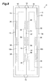
- FIG. 8 is a plan view showing the semiconductor photodetecting device according to the second embodiment.
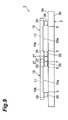
- Fig. 9 is a drawing for explaining a cross-sectional configuration of the semiconductor photodetecting device according to the second embodiment.
- the semiconductor photodetecting device 2 has a base 3, and a plurality of semiconductor photodetecting elements 10, as shown in Figs. 8 and 9 .
- the semiconductor photodetecting device 1 has two semiconductor photodetecting elements 10.
- the plurality of dummy bumps 37 are disposed so as to lie on each semiconductor photodetecting element 10 on the sides where the first sides 13 adjacent to each other lie in the adjacent semiconductor photodetecting elements 10.
- two dummy bumps 37 are disposed so as to lie on the adjacent semiconductor photodetecting elements 10, on the sides where the first sides 13 lie.
- the two dummy bumps 37 are disposed so as to lie on the adjacent semiconductor photodetecting elements 10, on the sides where the first sides 13 lie. Even if each semiconductor photodetecting element 10 comes close to undergoing the positional deviation due to the factor such as the contraction of the plurality of bump electrodes 35, each semiconductor photodetecting element 10 will be prevented from suffering the positional deviation, because the dummy bumps 37 are disposed each so as to lie on each semiconductor photodetecting element 10 on the sides where the first sides 13 lie. Therefore, the two semiconductor photodetecting elements 10 are disposed with high position accuracy.
- Each of the modification examples shown in Figs. 6 and 7 also corresponds to a modification example of the present second embodiment, in that the plurality of dummy bumps 37 are disposed so as to lie on the adjacent semiconductor photodetecting elements 10, on the sides where the first sides 13 lie.
- the bump electrodes 35 and the dummy bumps 37 may be made using the same solder bumps or using different solder bumps.
- the dummy bumps 37 may be made using solder bumps with the melting point lower than that of the bump electrodes 35.
- the bump electrodes 35 start hardening earlier than the dummy bumps 37, while the dummy bumps 37 still remain molten. Therefore, the bump electrodes 35 become hardened while each semiconductor photodetecting element 10 is in alignment by surface tension of the dummy bumps 37. As a result, each semiconductor photodetecting element 10 is further prevented from suffering the positional deviation.
- the bump electrodes 35 and the dummy bumps 37 may be different in size.
- the dummy bumps 37 may be smaller than the bump electrodes 35.
- the dummy bumps 37 undergo contraction during the hardening process.
- a contraction percentage of the dummy bumps 37 is relatively small and an extremely small force is imposed on the semiconductor photodetecting elements 10 during the contraction thereof. Therefore, each semiconductor photodetecting element 10 is securely prevented from suffering the positional deviation.
- the dummy bumps 37 are the solder bumps with the melting point lower than that of the bump electrodes 35, each semiconductor photodetecting element 10 can be more securely prevented from suffering the positional deviation.
- Each semiconductor photodetecting element 10 is located so as to be adjacent to another in juxtaposition in the first direction on the principal surface 3a of the base 3, but does not have to be limited to this.
- each semiconductor photodetecting element 10 may be located so as to be adjacent to another in juxtaposition in the second direction on the principal surface 3a of the base 3.
- the second side 15 of one semiconductor photodetecting element 10 is adjacent to the second side 15 of the other semiconductor photodetecting element 10.
- the number of semiconductor photodetecting elements 10 does not have to be limited to the number described above, but the semiconductor photodetecting device 1 or 2 may have three or more semiconductor photodetecting elements 10.
- the numbers of bump electrodes 35 and dummy bumps 37 are not limited to the above-described numbers, either.
- the present invention is applicable to the semiconductor photodetecting devices having a plurality of semiconductor photodetecting elements.
Landscapes
- Solid State Image Pick-Up Elements (AREA)
- Physics & Mathematics (AREA)
- Geometry (AREA)
- Light Receiving Elements (AREA)
Abstract
Description
- The present invention relates to a semiconductor photodetecting device including a plurality of semiconductor photodetecting elements.
- There is a known semiconductor photodetecting device including a base, a plurality of semiconductor photodetecting elements disposed on the base, and a plurality of bump electrodes electrically and mechanically connecting the base and each semiconductor photodetecting element (e.g., cf. Patent Literature 1). The plurality of semiconductor photodetecting elements have a planar shape having a pair of first sides opposed to each other in a first direction and a pair of second sides opposed to each other in a second direction perpendicular to the first direction. The plurality of semiconductor photodetecting elements are disposed on the base so as to be adjacent to each other in juxtaposition.
- Patent Literature 1:
Japanese Patent Application Laid-open Publication No. 2000-022120 - However, the semiconductor photodetecting device described in
Patent Literature 1 may have the problem as described below. The base and the plurality of semiconductor photodetecting elements are mechanically connected to each other when the bump electrodes become hardened. At this time, each semiconductor photodetecting element may suffer positional deviation due to a factor such as contraction of the bump electrodes occurring during the hardening process of the bump electrodes. - In the semiconductor photodetecting element having the planar shape with the pair of second sides shorter than the pair of first sides, a plurality of contact pads to which the corresponding bump electrodes are connected are disposed on the sides where the pair of first sides lie, in order to reduce the wiring capacity by use of shorter wires to the contact pads. At this time, in order to further reduce the wiring capacity, the plurality of contact pads are disposed at positions relatively distant from the second sides, when viewed in the second direction, in some cases. When the plurality of contact pads, i.e., the plurality of bump electrodes are disposed on the sides where the pair of first sides lie, the positional deviation of the semiconductor photodetecting element may increase on the sides where the second sides lie, during the contraction of these bump electrodes.
- It is an object of the present invention to provide a semiconductor photodetecting device in which a plurality of semiconductor photodetecting elements are disposed with high position accuracy.
- A semiconductor photodetecting device according to one aspect of the present invention includes a base; a plurality of semiconductor photodetecting elements that have a planar shape having a pair of first sides opposed to each other in a first direction and a pair of second sides being shorter than the pair of first sides and opposed to each other in a second direction perpendicular to the first direction, and that are disposed on the base so as to be adjacent to each other in juxtaposition; a plurality of bump electrodes each disposed on sides where the pair of first sides lie in each semiconductor photodetecting element, to electrically and mechanically connect the base and each semiconductor photodetecting element; and a plurality of dummy bumps disposed so that at least one dummy bump is disposed on each of sides where the pair of second sides lie in each semiconductor photodetecting element, to mechanically connect the base and each semiconductor photodetecting element.
- In the semiconductor photodetecting device according to the one aspect of the present invention, at least one dummy bump is disposed on each of the sides where the pair of second sides lie in each semiconductor photodetecting element. Even if each semiconductor photodetecting element comes close to undergoing the positional deviation due to the factor such as the contraction of the plurality of bump electrodes, each semiconductor photodetecting element will be prevented from suffering the positional deviation, because the dummy bumps are disposed one on each of the sides where the pair of second sides lie. Therefore, the plurality of semiconductor photodetecting elements are disposed with high position accuracy.
- Each semiconductor photodetecting element may be adjacent to another in juxtaposition in the first direction. When each semiconductor photodetecting element is disposed so as to be adjacent to another in juxtaposition in the first direction, it can undergo positional deviation due to a factor such as interference between the semiconductor photodetecting elements. However, since the dummy bumps are disposed one on each of the sides where the pair of second sides lie, even if each semiconductor photodetecting element comes close to undergoing the positional deviation due to the factor such as the interference between the semiconductor photodetecting elements in the configuration wherein each semiconductor photodetecting element is disposed so as to be adjacent to another in juxtaposition in the first direction, occurrence of the positional deviation can be securely prevented.
- The plurality of dummy bumps may be disposed so as to lie on the plurality of adjacent semiconductor photodetecting elements. In this case, the plurality of dummy bumps are shared among the adjacent semiconductor photodetecting elements. As a result, the number of dummy bumps can be made relatively small and thus increase in cost can be suppressed.
- The semiconductor photodetecting device may further include at least one dummy bump that is disposed so as to lie on each semiconductor photodetecting element on a side where sides adjacent to each other lie in the plurality of adjacent semiconductor photodetecting elements, out of the first sides and the second sides, to mechanically connect the base and each semiconductor photodetecting element. In this case, each semiconductor photodetecting element is further prevented from suffering the positional deviation and thus the plurality of semiconductor photodetecting elements are disposed with higher position accuracy.
- A semiconductor photodetecting device according to another aspect of the present invention includes a base; a plurality of semiconductor photodetecting elements that have a planar shape having a pair of first sides opposed to each other in a first direction and a pair of second sides opposed to each other in a second direction perpendicular to the first direction, and that are disposed on the base so as to be adjacent to each other in juxtaposition in the first direction; a plurality of bump electrodes each disposed on sides where the pair of first sides lie in each semiconductor photodetecting element, to electrically and mechanically connect the base and each semiconductor photodetecting element; and a plurality of dummy bumps disposed so as to lie on each semiconductor photodetecting element on sides where the first sides adjacent to each other lie in the plurality of adjacent semiconductor photodetecting elements, to mechanically connect the base and each semiconductor photodetecting element.
- In the semiconductor photodetecting device according to the other aspect of the present invention, the plurality of dummy bumps are disposed so as to lie on each semiconductor photodetecting element on the sides where the first sides adjacent to each other lie in the plurality of adjacent semiconductor photodetecting elements. Even if each semiconductor photodetecting element comes close to undergoing the positional deviation due to the factor such as the contraction of the plurality of bump electrodes, each semiconductor photodetecting element will be prevented from suffering the positional deviation, because the dummy bumps are disposed each so as to lie on each semiconductor photodetecting element on the sides where the first sides lie. Therefore, the plurality of semiconductor photodetecting elements are disposed with high position accuracy.
- A plurality of contact pads that are formed by the same manufacturing process and to which the plurality of bump electrodes and the plurality of dummy bumps are connected may be disposed on the plurality of semiconductor photodetecting elements. In this case, position accuracy is kept extremely high for the contact pads to which the bump electrodes are connected and for the contact pads to which the dummy bumps are connected. Therefore, the plurality of semiconductor photodetecting elements can be disposed with higher position accuracy.
- The plurality of bump electrodes may be solder bumps, and the plurality of dummy bumps may be solder bumps with a melting point lower than that of the plurality of bump electrodes. In this case, the bump electrodes start hardening earlier than the dummy bumps, but the bump electrodes become hardened with each semiconductor photodetecting element being in alignment because the dummy bumps are still in a molten state. Therefore, each semiconductor photodetecting element can be further prevented from suffering the positional deviation.
- The plurality of dummy bumps may be smaller than the plurality of bump electrodes. Not only the bump electrodes but also the dummy bumps contract during the hardening process. However, since the dummy bumps are smaller than the bump electrodes, a contraction percentage of the dummy bumps is smaller and a force imposed on the semiconductor photodetecting elements during the contraction is very small. Therefore, each semiconductor photodetecting element can be securely prevented from suffering the positional deviation.
- Each semiconductor photodetecting element may be a solid-state imaging device capable of acquiring a two-dimensional image with a longitudinal direction along the second direction and being driven by TDI driving.
- The present invention has successfully provided the semiconductor photodetecting device in which the plurality of semiconductor photodetecting elements were disposed with high position accuracy.
-
-
Fig. 1 is a plan view showing a semiconductor photodetecting device according to a first embodiment. -
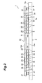
Fig. 2 is a drawing for explaining a cross-sectional configuration of the semiconductor photodetecting device according to the first embodiment. -
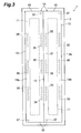
Fig. 3 is a plan view showing a semiconductor photodetecting device according to a modification example of the first embodiment. -
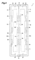
Fig. 4 is a plan view showing a semiconductor photodetecting device according to a modification example of the first embodiment. -
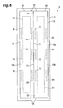
Fig. 5 is a plan view showing a semiconductor photodetecting device according to a modification example of the first embodiment. -
Fig. 6 is a plan view showing a semiconductor photodetecting device according to a modification example of the first embodiment. -
Fig. 7 is a plan view showing a semiconductor photodetecting device according to a modification example of the first embodiment. -
Fig. 8 is a plan view showing a semiconductor photodetecting device according to a second embodiment. -
Fig. 9 is a drawing for explaining a cross-sectional configuration of the semiconductor photodetecting device according to the second embodiment. -
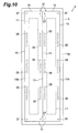
Fig. 10 is a plan view showing a semiconductor photodetecting device according to a modification example of the first embodiment. -
Fig. 11 is a plan view showing a semiconductor photodetecting device according to a modification example of the second embodiment. - Embodiments of the present invention will be described below in detail with reference to the accompanying drawings. Identical elements or elements with identical functionality will be denoted by the same reference signs in the description, without redundant description.
- A configuration of the semiconductor photodetecting
device 1 according to the first embodiment will be described with reference toFigs. 1 and2 .Fig. 1 is a plan view showing the semiconductor photodetecting device according to the first embodiment.Fig. 2 is a drawing for explaining a cross-sectional configuration of the semiconductor photodetecting device according to the first embodiment. - The
semiconductor photodetecting device 1 has abase 3, and a plurality ofsemiconductor photodetecting elements 10, as shown inFigs. 1 and2 . In the present embodiment, thesemiconductor photodetecting device 1 has twosemiconductor photodetecting elements 10. - The
base 3 is a substrate that hasprincipal surfaces contact pads 5 andcontact pads 7 are disposed on theprincipal surface 3 a. Theprincipal surface 3 a is a surface for eachsemiconductor photodetecting element 10 to be disposed thereon. Namely, eachsemiconductor photodetecting element 10 is disposed on theprincipal surface 3 a of thebase 3. - Each
semiconductor photodetecting element 10 has aprincipal surface 10a and aprincipal surface 10b opposed to each other. Eachsemiconductor photodetecting element 10 is provided with aphotosensitive region 11 on theprincipal surface 10a side. Thephotosensitive region 11 generates an electric charge according to incident light. Eachsemiconductor photodetecting element 10 has a planar shape having a pair offirst sides 13 opposed to each other in a first direction and a pair ofsecond sides 15 being shorter than the pair offirst sides 13 and opposed to each other in a second direction perpendicular to the first direction. The present embodiment is configured by adopting a rectangle shape as the foregoing planar shape. Namely, eachfirst side 13 corresponds to a long side and eachsecond side 15 to a short side. Therefore, the first direction is a direction parallel to the short sides and the second direction a direction parallel to the long sides. - In the present embodiment, the
semiconductor photodetecting elements 10 used are BT (Back-illuminated Thinning)-CCDs (Charge Coupled Devices). Electric charges generated are transferred as signal charges by a shift register and are converted into voltages corresponding to the signal charges to be output. Thesemiconductor photodetecting elements 10 are driven by the TDI (Time Delay Integration) mode to implement the charge transfer in the first direction. Namely, thesemiconductor photodetecting elements 10 are solid-state imaging devices capable of acquiring a two-dimensional image with the longitudinal direction along the second direction and being driven by the TDI driving. The semiconductor photodetecting device 1 (semiconductor photodetecting elements 10) images a subject relatively moving in the first direction. - Each
semiconductor photodetecting element 10 is disposed on thebase 3 so that a light entrance plane lies on theprincipal surface 10b side. The principal surfaces 10a of thesemiconductor photodetecting elements 10 and theprincipal surface 3a of thebase 3 are opposed to each other. Eachsemiconductor photodetecting element 10 is located so as to be adjacent to another in juxtaposition in the first direction on theprincipal surface 3 a of thebase 3. - Each
semiconductor photodetecting element 10 has a plurality ofcontact pads 25 andcontact pads 27. Eachcontact pad principal surface 10a side of thesemiconductor photodetecting element 10. Eachcontact pad 25 is a contact pad for input/output of signal into or from thesemiconductor photodetecting element 10. Eachcontact pad 27 is a contact pad that does not contribute to the input/output of signal into or from thesemiconductor photodetecting element 10. Thecontact pads 27 are so-called dummy pads. Eachcontact pad principal surface 10a side of thesemiconductor photodetecting element 10 by the same manufacturing process. - The plurality of
contact pads 25 are disposed each on the sides where the pair offirst sides 13 lie in eachsemiconductor photodetecting element 10. Thecontact pads 25 are placed side by side along thefirst side 13 on each of the sides where thefirst sides 13 lie. For making the wiring distance shorter to decrease the wiring capacity, thecontact pads 25 are disposed at positions relatively distant from thesecond sides 15, when viewed in the second direction. In the present embodiment, eighteen (6×3)contact pads 25 are provided on each of the sides where thefirst sides 13 lie. - The plurality of
contact pads 27 are disposed each on the sides where the pair ofsecond sides 15 lie in eachsemiconductor photodetecting element 10. In the present embodiment, they are placed side by side along thesecond side 15 on each of the sides where thesecond sides 15 lie. Eachcontact pad 27 is disposed at a position corresponding to a corner of the rectangle shape. In the present embodiment, twocontact pads 27 are provided on each of the sides where thesecond sides 15 lie. - The plurality of
contact pads 5 disposed on thebase 3 are provided so that their positions are defined so as to correspond to the plurality ofcontact pads 25 on thesemiconductor photodetecting elements 10. Eachcontact pad 5 is a contact pad for the input/output of signal into or from thesemiconductor photodetecting element 10. In the present embodiment, seventy two (18×4)contact pads 5 are provided on thebase 3. - The plurality of
contact pads 7 disposed on thebase 3 are provided so that their positions are defined so as to correspond to the plurality ofcontact pads 27 on thesemiconductor photodetecting elements 10. Eachcontact pad 7 is a contact pad that does not contribute to the input/output of signal into or from thesemiconductor photodetecting element 10. Thecontact pads 7 are so-called dummy pads as thecontact pads 27 are. In the present embodiment, eight (4×2)contact pads 7 are provided on thebase 3. - The
semiconductor photodetecting device 1 has a plurality ofbump electrodes 35 and a plurality of dummy bumps 37. Eachsemiconductor photodetecting element 10 is mounted on thebase 3 by the plurality ofbump electrodes 35 and dummy bumps 37. Namely, eachsemiconductor photodetecting element 10 is mounted on thebase 3 by flip-chip bonding. - Each
bump electrode 35 electrically and mechanically connects thebase 3 and eachsemiconductor photodetecting element 10. Each dummy bump 37 mechanically connects thebase 3 and eachsemiconductor photodetecting element 10. In the present embodiment, solder bumps are used as thebump electrodes 35 and the plurality of dummy pumps 37. A tin-silver-copper alloy (Sn-Ag-Cu) solder can be used for the solder bumps. Thebump electrodes 35 and the plurality of dummy bumps 37 can also be made using bumps such as gold bumps, nickel bumps, or copper bumps, besides the solder bumps. - Each
bump electrode 35 connects thecontact pad 5 and thecontact pad 25 corresponding to each other. Namely, the plurality ofbump electrodes 35 are disposed each on the sides where the pair offirst sides 13 lie in eachsemiconductor photodetecting element 10, corresponding to thecontact pads 25. Thebump electrodes 35 are placed side by side along thefirst side 13 on each of the sides where thefirst sides 13 lie. The number ofbump electrodes 35 is the same as the number of contact pads 25 (or contact pads 5). - Each
dummy bump 37 connects thecontact pad 7 and thecontact pad 27 corresponding to each other. Namely, the plurality of dummy bumps 37 are disposed each on the sides where the pair ofsecond sides 15 lie in eachsemiconductor photodetecting element 10, corresponding to thecontact pads 27. The dummy bumps 37 are placed side by side along thesecond side 15 on each of the sides where thesecond sides 15 lie. The number of dummy bumps 37 is the same as the number of contact pads 27 (or contact pads 7). Eachdummy bump 37 does not contribute to the input/output of signal into or from thesemiconductor photodetecting element 10. - In the present first embodiment, as described above, the dummy bumps 37 are disposed so that two dummy bumps 37 are disposed on each of the sides where the pair of
second sides 15 lie in eachsemiconductor photodetecting element 10. Even if eachsemiconductor photodetecting element 10 comes close to undergoing the positional deviation due to a factor such as contraction of the plurality ofbump electrodes 35, eachsemiconductor photodetecting element 10 will be prevented from suffering the positional deviation, because the dummy bumps 37 are disposed each on the sides where the pair ofsecond sides 15 lie. Therefore, the twosemiconductor photodetecting elements 10 are disposed with high position accuracy. - Each
semiconductor photodetecting element 10 is adjacent to another in juxtaposition in the first direction. In this case, positional deviation can occur because of a factor such as interference between thesemiconductor photodetecting elements 10. However, since the dummy bumps 37 are disposed each on the sides where the pair ofsecond sides 15 lie, as described above, even if eachsemiconductor photodetecting element 10 comes close to undergoing the positional deviation due to the factor such as the interference between thesemiconductor photodetecting elements 10, occurrence of the positional deviation can be securely prevented. - Each
contact pad 25 and eachcontact pad 27 are formed by the same manufacturing process. For this reason, the position accuracy is kept extremely high for thecontact pads 25 to which thebump electrodes 35 are connected and for thecontact pads 27 to which the dummy bumps 37 are connected. Therefore, eachsemiconductor photodetecting element 10 can be disposed with higher position accuracy. - Each
semiconductor photodetecting element 10 is the solid-state imaging device capable of being driven by the TDI driving, as described above, and a specific area of a subject is imaged by the same pixel row, among thesemiconductor photodetecting elements 10. In this case, if there were positional deviation of eachsemiconductor photodetecting element 10, the specific area of the subject would be imaged by different pixel rows, among thesemiconductor photodetecting elements 10. This would result in blurring an acquired image and degrading resolution eventually. In the present embodiment, however, eachsemiconductor photodetecting element 10 is disposed with high position accuracy while being prevented from undergoing the positional deviation, as described above, and thus the acquired image is prevented from being blurred, without degradation of resolution. - The below will describe configurations of the
semiconductor photodetecting devices 1 according to modification examples of the first embodiment, with reference toFigs. 3 to 7. Figs. 3 to 7 are plan views showing the semiconductor photodetecting devices according to the modification examples of the first embodiment. - In the modification example shown in
Fig. 3 , eachdummy bump 37 is disposed so that onedummy bump 37 is disposed on each of the sides where the pair ofsecond sides 15 lie. In the present modification example, eachdummy bump 37 is disposed at one of positions corresponding to a pair of corners located on a diagonal of the rectangle shape. - In the modification example shown in
Fig. 4 , eachdummy bump 37 is also disposed so that onedummy bump 37 is disposed on each of the sides where the pair ofsecond sides 15 lie. In the present modification example, eachdummy bump 37 is disposed at a position corresponding to a central portion of thesecond side 15. - In the modification example shown in
Fig. 5 , eachdummy bump 37 is disposed so that onedummy bump 37 is disposed on each of the sides where thesecond sides 15 at one end lie and so that two dummy bumps 37 are disposed on each of the sides where thesecond sides 15 at the other end lie. In the present modification example, the dummy bumps 37 disposed on the sides where thesecond sides 15 at one end lie are disposed at positions corresponding to the respective central portions of the pertinent second sides 15. Each dummy bump 37 disposed on each of the sides where thesecond sides 15 at the other end lie is disposed at one of positions corresponding to the corners of the rectangle shape on the sides where thesecond sides 15 at the other end lie. - In the modification examples shown in
Figs. 3 to 5 , just as in the aforementioned first embodiment, eachsemiconductor photodetecting element 10 is also prevented from undergoing the positional deviation and the twosemiconductor photodetecting elements 10 are also disposed with high position accuracy. In each of the modification examples, each of thecontact pads dummy bump 37 is connected is also disposed at the position corresponding to thedummy bump 37 though not shown. - In the modification example shown in
Fig. 6 , eachdummy bump 37 is disposed so as to lie on the adjacentsemiconductor photodetecting elements 10, on each of the sides where the pair ofsecond sides 15 lie. In the present modification example, just as in the aforementioned first embodiment, eachsemiconductor photodetecting element 10 is also prevented from suffering the positional deviation and the twosemiconductor photodetecting elements 10 are disposed with high position accuracy. Since the dummy bumps 37 are shared between the adjacentsemiconductor photodetecting elements 10, the number of dummy bumps 37 is relatively small. This can suppress increase in cost. In the present modification example as well, each of thecontact pads dummy bump 37 is connected is also disposed at the position corresponding to thedummy bump 37 though not shown. - In the modification example shown in
Fig. 7 , the plurality of dummy bumps 37 are also disposed on the sides where thefirst sides 13 lie, in addition to those on the sides where the pair ofsecond sides 15 lie. In the present modification example, the two dummy bumps 37 are disposed so as to lie on the adjacentsemiconductor photodetecting elements 10, on the sides where thefirst sides 13 lie. In the present modification example, eachsemiconductor photodetecting element 10 is further prevented from suffering the positional deviation and the twosemiconductor photodetecting elements 10 are disposed with high position accuracy. - A configuration of the semiconductor photodetecting device 2 according to the second embodiment will be described with reference to
Figs. 8 and9 .Fig. 8 is a plan view showing the semiconductor photodetecting device according to the second embodiment.Fig. 9 is a drawing for explaining a cross-sectional configuration of the semiconductor photodetecting device according to the second embodiment. - The semiconductor photodetecting device 2 has a
base 3, and a plurality ofsemiconductor photodetecting elements 10, as shown inFigs. 8 and9 . In the present embodiment, thesemiconductor photodetecting device 1 has twosemiconductor photodetecting elements 10. - The plurality of dummy bumps 37 are disposed so as to lie on each
semiconductor photodetecting element 10 on the sides where thefirst sides 13 adjacent to each other lie in the adjacentsemiconductor photodetecting elements 10. In the present second embodiment, two dummy bumps 37 are disposed so as to lie on the adjacentsemiconductor photodetecting elements 10, on the sides where thefirst sides 13 lie. - In the present second embodiment, as described above, the two dummy bumps 37 are disposed so as to lie on the adjacent
semiconductor photodetecting elements 10, on the sides where thefirst sides 13 lie. Even if eachsemiconductor photodetecting element 10 comes close to undergoing the positional deviation due to the factor such as the contraction of the plurality ofbump electrodes 35, eachsemiconductor photodetecting element 10 will be prevented from suffering the positional deviation, because the dummy bumps 37 are disposed each so as to lie on eachsemiconductor photodetecting element 10 on the sides where thefirst sides 13 lie. Therefore, the twosemiconductor photodetecting elements 10 are disposed with high position accuracy. - Each of the modification examples shown in
Figs. 6 and7 also corresponds to a modification example of the present second embodiment, in that the plurality of dummy bumps 37 are disposed so as to lie on the adjacentsemiconductor photodetecting elements 10, on the sides where thefirst sides 13 lie. - The above described the embodiments of the present invention but it should be noted that the present invention does not always have to be limited to the foregoing embodiments and can be modified in many ways without departing from the scope and spirit of the invention.
- The
bump electrodes 35 and the dummy bumps 37 may be made using the same solder bumps or using different solder bumps. For example, the dummy bumps 37 may be made using solder bumps with the melting point lower than that of thebump electrodes 35. In this case, thebump electrodes 35 start hardening earlier than the dummy bumps 37, while the dummy bumps 37 still remain molten. Therefore, thebump electrodes 35 become hardened while eachsemiconductor photodetecting element 10 is in alignment by surface tension of the dummy bumps 37. As a result, eachsemiconductor photodetecting element 10 is further prevented from suffering the positional deviation. - The
bump electrodes 35 and the dummy bumps 37 may be different in size. For example, as shown inFigs. 10 and11 , the dummy bumps 37 may be smaller than thebump electrodes 35. Not only thebump electrodes 35 but also the dummy bumps 37 undergo contraction during the hardening process. However, since the dummy bumps 37 are made smaller than thebump electrodes 35, a contraction percentage of the dummy bumps 37 is relatively small and an extremely small force is imposed on thesemiconductor photodetecting elements 10 during the contraction thereof. Therefore, eachsemiconductor photodetecting element 10 is securely prevented from suffering the positional deviation. When the dummy bumps 37 are the solder bumps with the melting point lower than that of thebump electrodes 35, eachsemiconductor photodetecting element 10 can be more securely prevented from suffering the positional deviation. - Each
semiconductor photodetecting element 10 is located so as to be adjacent to another in juxtaposition in the first direction on theprincipal surface 3a of thebase 3, but does not have to be limited to this. For example, eachsemiconductor photodetecting element 10 may be located so as to be adjacent to another in juxtaposition in the second direction on theprincipal surface 3a of thebase 3. In this case, thesecond side 15 of onesemiconductor photodetecting element 10 is adjacent to thesecond side 15 of the othersemiconductor photodetecting element 10. - The number of
semiconductor photodetecting elements 10 does not have to be limited to the number described above, but thesemiconductor photodetecting device 1 or 2 may have three or moresemiconductor photodetecting elements 10. The numbers ofbump electrodes 35 and dummy bumps 37 are not limited to the above-described numbers, either. - The present invention is applicable to the semiconductor photodetecting devices having a plurality of semiconductor photodetecting elements.
- 1, 2 semiconductor photodetecting devices; 3 base; 5, 7 contact pads; 10 semiconductor photodetecting elements; 13 first sides; 15 second sides; 25, 27 contact pads; 35 bump electrodes; 37 dummy bumps.
Claims (9)
- A semiconductor photodetecting device, comprising:a base;a plurality of semiconductor photodetecting elements that have a planar shape having a pair of first sides opposed to each other in a first direction and a pair of second sides being shorter than the pair of first sides and opposed to each other in a second direction perpendicular to the first direction, and that are disposed on the base so as to be adjacent to each other in juxtaposition;a plurality of bump electrodes each disposed on sides where the pair of first sides lie in each said semiconductor photodetecting element, to electrically and mechanically connect the base and each said semiconductor photodetecting element; anda plurality of dummy bumps disposed so that at least one dummy bump is disposed on each of sides where the pair of second sides lie in each said semiconductor photodetecting element, to mechanically connect the base and each said semiconductor photodetecting element.
- The semiconductor photodetecting device according to claim 1,
wherein each said semiconductor photodetecting element is adjacent to another in juxtaposition in the first direction. - The semiconductor photodetecting device according to claim 1 or 2,
wherein the plurality of dummy bumps are disposed so as to lie on the plurality of adjacent semiconductor photodetecting elements. - The semiconductor photodetecting device according to any one of claims 1 to 3, further comprising:at least one dummy bump that is disposed so as to lie on each said semiconductor photodetecting element on a side where sides adjacent to each other lie in the plurality of adjacent semiconductor photodetecting elements, out of the first sides and the second sides, to mechanically connect the base and each said semiconductor photodetecting element.
- A semiconductor photodetecting device, comprising:a base;a plurality of semiconductor photodetecting elements that have a planar shape having a pair of first sides opposed to each other in a first direction and a pair of second sides opposed to each other in a second direction perpendicular to the first direction, and that are disposed on the base so as to be adjacent to each other in juxtaposition in the first direction;a plurality of bump electrodes each disposed on sides where the pair of first sides lie in each said semiconductor photodetecting element, to electrically and mechanically connect the base and each said semiconductor photodetecting element; anda plurality of dummy bumps disposed so as to lie on each said semiconductor photodetecting element on sides where the first sides adjacent to each other lie in the plurality of adjacent semiconductor photodetecting elements, to mechanically connect the base and each said semiconductor photodetecting element.
- The semiconductor photodetecting device according to any one of claims 1 to 5,
wherein a plurality of contact pads that are formed by the same manufacturing process and to which the plurality of bump electrodes and the plurality of dummy bumps are connected are disposed on the plurality of semiconductor photodetecting elements. - The semiconductor photodetecting device according to any one of claims 1 to 6,
wherein the plurality of bump electrodes are solder bumps, and wherein the plurality of dummy bumps are solder bumps with a melting point lower than that of the plurality of bump electrodes. - The semiconductor photodetecting device according to any one of claims 1 to 7,
wherein the plurality of dummy bumps are smaller than the plurality of bump electrodes. - The semiconductor photodetecting device according to any one of claims 1 to 8,
wherein each said semiconductor photodetecting element is a solid-state imaging device capable of acquiring a two-dimensional image with a longitudinal direction along the second direction and being driven by TDI driving.
Applications Claiming Priority (2)
| Application Number | Priority Date | Filing Date | Title |
|---|---|---|---|
| JP2013039333A JP6002062B2 (en) | 2013-02-28 | 2013-02-28 | Semiconductor photodetection device |
| PCT/JP2013/078221 WO2014132482A1 (en) | 2013-02-28 | 2013-10-17 | Semiconductor photodetection device |
Publications (3)
| Publication Number | Publication Date |
|---|---|
| EP2963686A1 true EP2963686A1 (en) | 2016-01-06 |
| EP2963686A4 EP2963686A4 (en) | 2016-10-26 |
| EP2963686B1 EP2963686B1 (en) | 2021-04-21 |
Family
ID=51427776
Family Applications (1)
| Application Number | Title | Priority Date | Filing Date |
|---|---|---|---|
| EP13876185.3A Active EP2963686B1 (en) | 2013-02-28 | 2013-10-17 | Semiconductor photodetection device |
Country Status (7)
| Country | Link |
|---|---|
| US (1) | US10199418B2 (en) |
| EP (1) | EP2963686B1 (en) |
| JP (1) | JP6002062B2 (en) |
| KR (1) | KR102059233B1 (en) |
| CN (1) | CN105074925B (en) |
| TW (1) | TWI612646B (en) |
| WO (1) | WO2014132482A1 (en) |
Families Citing this family (3)
| Publication number | Priority date | Publication date | Assignee | Title |
|---|---|---|---|---|
| US10177032B2 (en) * | 2014-06-18 | 2019-01-08 | Taiwan Semiconductor Manufacturing Company, Ltd. | Devices, packaging devices, and methods of packaging semiconductor devices |
| US10748857B2 (en) * | 2018-09-11 | 2020-08-18 | Micron Technology, Inc. | Die features for self-alignment during die bonding |
| US12332490B2 (en) * | 2021-09-24 | 2025-06-17 | Hirose Electric Co., Ltd. | Media adaptor for multimode waveguide interconnects |
Family Cites Families (18)
| Publication number | Priority date | Publication date | Assignee | Title |
|---|---|---|---|---|
| JPH06112463A (en) * | 1992-09-25 | 1994-04-22 | Mitsubishi Electric Corp | Semiconductor device and mounting method thereof |
| JP2853641B2 (en) * | 1996-02-27 | 1999-02-03 | 日本電気株式会社 | Light receiving device |
| JP3545247B2 (en) | 1998-04-27 | 2004-07-21 | シャープ株式会社 | 2D image detector |
| JP2000278605A (en) * | 1999-03-29 | 2000-10-06 | Canon Inc | Imaging device and image processing system |
| JP2002026302A (en) * | 2000-07-11 | 2002-01-25 | Canon Inc | Radiation imaging apparatus and manufacturing method thereof |
| US6828541B2 (en) * | 2000-07-18 | 2004-12-07 | Nippon Sheet Glass Co., Ltd. | Light receiving element array having isolated pin photodiodes |
| US20040012684A1 (en) | 2002-07-16 | 2004-01-22 | Fairchild Imaging | Image reconstruction techniques for charge coupled devices |
| JP4264381B2 (en) * | 2004-04-30 | 2009-05-13 | 株式会社モリタ製作所 | Two-dimensional image processing method of solid-state image sensor and medical digital X-ray imaging apparatus |
| CN101010807A (en) | 2004-09-02 | 2007-08-01 | 阿帕托佩克股份有限公司 | Method of making camera module in wafer level |
| JP2006222374A (en) | 2005-02-14 | 2006-08-24 | Fuji Film Microdevices Co Ltd | Semiconductor chip |
| JP2006287640A (en) * | 2005-03-31 | 2006-10-19 | Fuji Photo Film Co Ltd | Solid-state image pickup device package, solid-state image pickup device mounting board, digital camera, and solid-state image pickup device mounting method |
| JP2007149851A (en) | 2005-11-25 | 2007-06-14 | Sony Computer Entertainment Inc | Wiring board, electronic component mounting structure, and electronic component mounting method |
| US7791016B2 (en) * | 2007-10-29 | 2010-09-07 | Hamamatsu Photonics K.K. | Photodetector |
| JP4997066B2 (en) * | 2007-10-29 | 2012-08-08 | 浜松ホトニクス株式会社 | Photodetector |
| DE102008050840A1 (en) | 2008-10-08 | 2009-10-15 | Siemens Aktiengesellschaft | Electrical module i.e. detector module, manufacturing method for X-ray measuring system of computer tomography scanner, involves soldering evaluation electronics of component with carrier substrate by low-temperature-guide |
| JP5671849B2 (en) * | 2010-06-24 | 2015-02-18 | 住友電気工業株式会社 | Light receiving element array, hybrid detection device, and optical sensor device |
| IT1402806B1 (en) * | 2010-11-29 | 2013-09-18 | St Microelectronics Srl | PHOTOMOLTIPLICATOR INCAPSULATED BY SEMICONDUCTOR MATERIAL, IN PARTICULAR FOR USE IN MACHINES FOR THE PERFORMANCE OF TOMOGRAPHY WITH POSITRON EMISSION. |
| JP5600642B2 (en) * | 2011-06-16 | 2014-10-01 | 株式会社日立製作所 | Manufacturing method of semiconductor device |
-
2013
- 2013-02-28 JP JP2013039333A patent/JP6002062B2/en active Active
- 2013-10-17 EP EP13876185.3A patent/EP2963686B1/en active Active
- 2013-10-17 CN CN201380073748.8A patent/CN105074925B/en active Active
- 2013-10-17 US US14/766,336 patent/US10199418B2/en active Active
- 2013-10-17 WO PCT/JP2013/078221 patent/WO2014132482A1/en not_active Ceased
- 2013-10-17 KR KR1020157025788A patent/KR102059233B1/en active Active
- 2013-11-06 TW TW102140330A patent/TWI612646B/en active
Also Published As
| Publication number | Publication date |
|---|---|
| CN105074925B (en) | 2018-04-13 |
| JP2014167982A (en) | 2014-09-11 |
| EP2963686B1 (en) | 2021-04-21 |
| JP6002062B2 (en) | 2016-10-05 |
| EP2963686A4 (en) | 2016-10-26 |
| WO2014132482A1 (en) | 2014-09-04 |
| KR102059233B1 (en) | 2019-12-24 |
| TWI612646B (en) | 2018-01-21 |
| US10199418B2 (en) | 2019-02-05 |
| TW201434140A (en) | 2014-09-01 |
| CN105074925A (en) | 2015-11-18 |
| US20150380455A1 (en) | 2015-12-31 |
| KR20150125970A (en) | 2015-11-10 |
Similar Documents
| Publication | Publication Date | Title |
|---|---|---|
| US20210028205A1 (en) | Solid-state imaging device and electronic apparatus | |
| US9583526B2 (en) | Solid-state image pickup element and solid-state image pickup element mounting structure | |
| US8982275B2 (en) | Imaging apparatus | |
| US9865641B2 (en) | Solid-state imaging device, manufacturing method therefor, and imaging apparatus | |
| US10199418B2 (en) | Semiconductor photodetection device | |
| JP6732043B2 (en) | TDI linear image sensor | |
| US12225304B2 (en) | Expanded image sensor pixel array | |
| CN100463206C (en) | Solid-state imaging device | |
| US10341597B2 (en) | Solid-state imaging device, method for manufacturing solid-state imaging device, and electronic apparatus | |
| CN118632142A (en) | Image sensor signal path routing | |
| JP2013175540A (en) | Solid state image pickup device and manufacturing method of the same | |
| US8334578B2 (en) | Integrated circuit having wiring structure, solid image pickup element having the wiring structure, and imaging device having the solid image pickup element | |
| JP6349089B2 (en) | Semiconductor device and imaging module | |
| JP2012009790A (en) | Solid-state imaging device |
Legal Events
| Date | Code | Title | Description |
|---|---|---|---|
| PUAI | Public reference made under article 153(3) epc to a published international application that has entered the european phase |
Free format text: ORIGINAL CODE: 0009012 |
|
| 17P | Request for examination filed |
Effective date: 20150706 |
|
| AK | Designated contracting states |
Kind code of ref document: A1 Designated state(s): AL AT BE BG CH CY CZ DE DK EE ES FI FR GB GR HR HU IE IS IT LI LT LU LV MC MK MT NL NO PL PT RO RS SE SI SK SM TR |
|
| AX | Request for extension of the european patent |
Extension state: BA ME |
|
| DAX | Request for extension of the european patent (deleted) | ||
| A4 | Supplementary search report drawn up and despatched |
Effective date: 20160926 |
|
| RIC1 | Information provided on ipc code assigned before grant |
Ipc: H01L 23/498 20060101ALN20160920BHEP Ipc: H01L 23/12 20060101ALI20160920BHEP Ipc: H01L 27/146 20060101AFI20160920BHEP Ipc: H01L 31/02 20060101ALI20160920BHEP |
|
| STAA | Information on the status of an ep patent application or granted ep patent |
Free format text: STATUS: EXAMINATION IS IN PROGRESS |
|
| 17Q | First examination report despatched |
Effective date: 20200211 |
|
| REG | Reference to a national code |
Ref country code: DE Ref legal event code: R079 Ref document number: 602013077080 Country of ref document: DE Free format text: PREVIOUS MAIN CLASS: H01L0027140000 Ipc: H01L0027146000 |
|
| GRAP | Despatch of communication of intention to grant a patent |
Free format text: ORIGINAL CODE: EPIDOSNIGR1 |
|
| STAA | Information on the status of an ep patent application or granted ep patent |
Free format text: STATUS: GRANT OF PATENT IS INTENDED |
|
| RIC1 | Information provided on ipc code assigned before grant |
Ipc: H01L 23/498 20060101ALN20201123BHEP Ipc: H01L 31/02 20060101ALI20201123BHEP Ipc: H01L 23/12 20060101ALI20201123BHEP Ipc: H01L 27/146 20060101AFI20201123BHEP |
|
| RIC1 | Information provided on ipc code assigned before grant |
Ipc: H01L 23/498 20060101ALN20201130BHEP Ipc: H01L 31/02 20060101ALI20201130BHEP Ipc: H01L 23/12 20060101ALI20201130BHEP Ipc: H01L 27/146 20060101AFI20201130BHEP |
|
| INTG | Intention to grant announced |
Effective date: 20201216 |
|
| GRAS | Grant fee paid |
Free format text: ORIGINAL CODE: EPIDOSNIGR3 |
|
| GRAA | (expected) grant |
Free format text: ORIGINAL CODE: 0009210 |
|
| STAA | Information on the status of an ep patent application or granted ep patent |
Free format text: STATUS: THE PATENT HAS BEEN GRANTED |
|
| AK | Designated contracting states |
Kind code of ref document: B1 Designated state(s): AL AT BE BG CH CY CZ DE DK EE ES FI FR GB GR HR HU IE IS IT LI LT LU LV MC MK MT NL NO PL PT RO RS SE SI SK SM TR |
|
| REG | Reference to a national code |
Ref country code: GB Ref legal event code: FG4D |
|
| REG | Reference to a national code |
Ref country code: CH Ref legal event code: EP |
|
| REG | Reference to a national code |
Ref country code: DE Ref legal event code: R096 Ref document number: 602013077080 Country of ref document: DE |
|
| REG | Reference to a national code |
Ref country code: IE Ref legal event code: FG4D |
|
| REG | Reference to a national code |
Ref country code: AT Ref legal event code: REF Ref document number: 1385547 Country of ref document: AT Kind code of ref document: T Effective date: 20210515 |
|
| REG | Reference to a national code |
Ref country code: LT Ref legal event code: MG9D |
|
| REG | Reference to a national code |
Ref country code: AT Ref legal event code: MK05 Ref document number: 1385547 Country of ref document: AT Kind code of ref document: T Effective date: 20210421 |
|
| REG | Reference to a national code |
Ref country code: NL Ref legal event code: MP Effective date: 20210421 |
|
| PG25 | Lapsed in a contracting state [announced via postgrant information from national office to epo] |
Ref country code: HR Free format text: LAPSE BECAUSE OF FAILURE TO SUBMIT A TRANSLATION OF THE DESCRIPTION OR TO PAY THE FEE WITHIN THE PRESCRIBED TIME-LIMIT Effective date: 20210421 Ref country code: BG Free format text: LAPSE BECAUSE OF FAILURE TO SUBMIT A TRANSLATION OF THE DESCRIPTION OR TO PAY THE FEE WITHIN THE PRESCRIBED TIME-LIMIT Effective date: 20210721 Ref country code: AT Free format text: LAPSE BECAUSE OF FAILURE TO SUBMIT A TRANSLATION OF THE DESCRIPTION OR TO PAY THE FEE WITHIN THE PRESCRIBED TIME-LIMIT Effective date: 20210421 Ref country code: FI Free format text: LAPSE BECAUSE OF FAILURE TO SUBMIT A TRANSLATION OF THE DESCRIPTION OR TO PAY THE FEE WITHIN THE PRESCRIBED TIME-LIMIT Effective date: 20210421 Ref country code: NL Free format text: LAPSE BECAUSE OF FAILURE TO SUBMIT A TRANSLATION OF THE DESCRIPTION OR TO PAY THE FEE WITHIN THE PRESCRIBED TIME-LIMIT Effective date: 20210421 Ref country code: LT Free format text: LAPSE BECAUSE OF FAILURE TO SUBMIT A TRANSLATION OF THE DESCRIPTION OR TO PAY THE FEE WITHIN THE PRESCRIBED TIME-LIMIT Effective date: 20210421 |
|
| PG25 | Lapsed in a contracting state [announced via postgrant information from national office to epo] |
Ref country code: GR Free format text: LAPSE BECAUSE OF FAILURE TO SUBMIT A TRANSLATION OF THE DESCRIPTION OR TO PAY THE FEE WITHIN THE PRESCRIBED TIME-LIMIT Effective date: 20210722 Ref country code: LV Free format text: LAPSE BECAUSE OF FAILURE TO SUBMIT A TRANSLATION OF THE DESCRIPTION OR TO PAY THE FEE WITHIN THE PRESCRIBED TIME-LIMIT Effective date: 20210421 Ref country code: IS Free format text: LAPSE BECAUSE OF FAILURE TO SUBMIT A TRANSLATION OF THE DESCRIPTION OR TO PAY THE FEE WITHIN THE PRESCRIBED TIME-LIMIT Effective date: 20210821 Ref country code: PL Free format text: LAPSE BECAUSE OF FAILURE TO SUBMIT A TRANSLATION OF THE DESCRIPTION OR TO PAY THE FEE WITHIN THE PRESCRIBED TIME-LIMIT Effective date: 20210421 Ref country code: PT Free format text: LAPSE BECAUSE OF FAILURE TO SUBMIT A TRANSLATION OF THE DESCRIPTION OR TO PAY THE FEE WITHIN THE PRESCRIBED TIME-LIMIT Effective date: 20210823 Ref country code: NO Free format text: LAPSE BECAUSE OF FAILURE TO SUBMIT A TRANSLATION OF THE DESCRIPTION OR TO PAY THE FEE WITHIN THE PRESCRIBED TIME-LIMIT Effective date: 20210721 Ref country code: ES Free format text: LAPSE BECAUSE OF FAILURE TO SUBMIT A TRANSLATION OF THE DESCRIPTION OR TO PAY THE FEE WITHIN THE PRESCRIBED TIME-LIMIT Effective date: 20210421 Ref country code: RS Free format text: LAPSE BECAUSE OF FAILURE TO SUBMIT A TRANSLATION OF THE DESCRIPTION OR TO PAY THE FEE WITHIN THE PRESCRIBED TIME-LIMIT Effective date: 20210421 Ref country code: SE Free format text: LAPSE BECAUSE OF FAILURE TO SUBMIT A TRANSLATION OF THE DESCRIPTION OR TO PAY THE FEE WITHIN THE PRESCRIBED TIME-LIMIT Effective date: 20210421 |
|
| REG | Reference to a national code |
Ref country code: DE Ref legal event code: R097 Ref document number: 602013077080 Country of ref document: DE |
|
| PG25 | Lapsed in a contracting state [announced via postgrant information from national office to epo] |
Ref country code: RO Free format text: LAPSE BECAUSE OF FAILURE TO SUBMIT A TRANSLATION OF THE DESCRIPTION OR TO PAY THE FEE WITHIN THE PRESCRIBED TIME-LIMIT Effective date: 20210421 Ref country code: CZ Free format text: LAPSE BECAUSE OF FAILURE TO SUBMIT A TRANSLATION OF THE DESCRIPTION OR TO PAY THE FEE WITHIN THE PRESCRIBED TIME-LIMIT Effective date: 20210421 Ref country code: EE Free format text: LAPSE BECAUSE OF FAILURE TO SUBMIT A TRANSLATION OF THE DESCRIPTION OR TO PAY THE FEE WITHIN THE PRESCRIBED TIME-LIMIT Effective date: 20210421 Ref country code: DK Free format text: LAPSE BECAUSE OF FAILURE TO SUBMIT A TRANSLATION OF THE DESCRIPTION OR TO PAY THE FEE WITHIN THE PRESCRIBED TIME-LIMIT Effective date: 20210421 Ref country code: SK Free format text: LAPSE BECAUSE OF FAILURE TO SUBMIT A TRANSLATION OF THE DESCRIPTION OR TO PAY THE FEE WITHIN THE PRESCRIBED TIME-LIMIT Effective date: 20210421 Ref country code: SM Free format text: LAPSE BECAUSE OF FAILURE TO SUBMIT A TRANSLATION OF THE DESCRIPTION OR TO PAY THE FEE WITHIN THE PRESCRIBED TIME-LIMIT Effective date: 20210421 |
|
| PLBE | No opposition filed within time limit |
Free format text: ORIGINAL CODE: 0009261 |
|
| STAA | Information on the status of an ep patent application or granted ep patent |
Free format text: STATUS: NO OPPOSITION FILED WITHIN TIME LIMIT |
|
| 26N | No opposition filed |
Effective date: 20220124 |
|
| REG | Reference to a national code |
Ref country code: CH Ref legal event code: PL |
|
| PG25 | Lapsed in a contracting state [announced via postgrant information from national office to epo] |
Ref country code: IS Free format text: LAPSE BECAUSE OF FAILURE TO SUBMIT A TRANSLATION OF THE DESCRIPTION OR TO PAY THE FEE WITHIN THE PRESCRIBED TIME-LIMIT Effective date: 20210821 Ref country code: AL Free format text: LAPSE BECAUSE OF FAILURE TO SUBMIT A TRANSLATION OF THE DESCRIPTION OR TO PAY THE FEE WITHIN THE PRESCRIBED TIME-LIMIT Effective date: 20210421 |
|
| REG | Reference to a national code |
Ref country code: BE Ref legal event code: MM Effective date: 20211031 |
|
| PG25 | Lapsed in a contracting state [announced via postgrant information from national office to epo] |
Ref country code: MC Free format text: LAPSE BECAUSE OF FAILURE TO SUBMIT A TRANSLATION OF THE DESCRIPTION OR TO PAY THE FEE WITHIN THE PRESCRIBED TIME-LIMIT Effective date: 20210421 |
|
| PG25 | Lapsed in a contracting state [announced via postgrant information from national office to epo] |
Ref country code: LU Free format text: LAPSE BECAUSE OF NON-PAYMENT OF DUE FEES Effective date: 20211017 Ref country code: IT Free format text: LAPSE BECAUSE OF FAILURE TO SUBMIT A TRANSLATION OF THE DESCRIPTION OR TO PAY THE FEE WITHIN THE PRESCRIBED TIME-LIMIT Effective date: 20210421 Ref country code: BE Free format text: LAPSE BECAUSE OF NON-PAYMENT OF DUE FEES Effective date: 20211031 |
|
| PG25 | Lapsed in a contracting state [announced via postgrant information from national office to epo] |
Ref country code: LI Free format text: LAPSE BECAUSE OF NON-PAYMENT OF DUE FEES Effective date: 20211031 Ref country code: CH Free format text: LAPSE BECAUSE OF NON-PAYMENT OF DUE FEES Effective date: 20211031 |
|
| PG25 | Lapsed in a contracting state [announced via postgrant information from national office to epo] |
Ref country code: IE Free format text: LAPSE BECAUSE OF NON-PAYMENT OF DUE FEES Effective date: 20211017 |
|
| PG25 | Lapsed in a contracting state [announced via postgrant information from national office to epo] |
Ref country code: HU Free format text: LAPSE BECAUSE OF FAILURE TO SUBMIT A TRANSLATION OF THE DESCRIPTION OR TO PAY THE FEE WITHIN THE PRESCRIBED TIME-LIMIT; INVALID AB INITIO Effective date: 20131017 |
|
| P01 | Opt-out of the competence of the unified patent court (upc) registered |
Effective date: 20230509 |
|
| PG25 | Lapsed in a contracting state [announced via postgrant information from national office to epo] |
Ref country code: CY Free format text: LAPSE BECAUSE OF FAILURE TO SUBMIT A TRANSLATION OF THE DESCRIPTION OR TO PAY THE FEE WITHIN THE PRESCRIBED TIME-LIMIT Effective date: 20210421 |
|
| PG25 | Lapsed in a contracting state [announced via postgrant information from national office to epo] |
Ref country code: MK Free format text: LAPSE BECAUSE OF FAILURE TO SUBMIT A TRANSLATION OF THE DESCRIPTION OR TO PAY THE FEE WITHIN THE PRESCRIBED TIME-LIMIT Effective date: 20210421 |
|
| PG25 | Lapsed in a contracting state [announced via postgrant information from national office to epo] |
Ref country code: TR Free format text: LAPSE BECAUSE OF FAILURE TO SUBMIT A TRANSLATION OF THE DESCRIPTION OR TO PAY THE FEE WITHIN THE PRESCRIBED TIME-LIMIT Effective date: 20210421 |
|
| PG25 | Lapsed in a contracting state [announced via postgrant information from national office to epo] |
Ref country code: MT Free format text: LAPSE BECAUSE OF FAILURE TO SUBMIT A TRANSLATION OF THE DESCRIPTION OR TO PAY THE FEE WITHIN THE PRESCRIBED TIME-LIMIT Effective date: 20210421 |
|
| REG | Reference to a national code |
Ref country code: DE Ref legal event code: R079 Ref document number: 602013077080 Country of ref document: DE Free format text: PREVIOUS MAIN CLASS: H01L0027146000 Ipc: H10F0039180000 |
|
| PGFP | Annual fee paid to national office [announced via postgrant information from national office to epo] |
Ref country code: GB Payment date: 20250828 Year of fee payment: 13 |
|
| PGFP | Annual fee paid to national office [announced via postgrant information from national office to epo] |
Ref country code: FR Payment date: 20250908 Year of fee payment: 13 |
|
| PGFP | Annual fee paid to national office [announced via postgrant information from national office to epo] |
Ref country code: DE Payment date: 20250902 Year of fee payment: 13 |