EP2962850A1 - Capacitive load driving circuit, ink jet printer, and fluid ejecting apparatus - Google Patents
Capacitive load driving circuit, ink jet printer, and fluid ejecting apparatus Download PDFInfo
- Publication number
- EP2962850A1 EP2962850A1 EP15178239.8A EP15178239A EP2962850A1 EP 2962850 A1 EP2962850 A1 EP 2962850A1 EP 15178239 A EP15178239 A EP 15178239A EP 2962850 A1 EP2962850 A1 EP 2962850A1
- Authority
- EP
- European Patent Office
- Prior art keywords
- signal
- capacitive load
- drive
- driving circuit
- attenuator
- Prior art date
- Legal status (The legal status is an assumption and is not a legal conclusion. Google has not performed a legal analysis and makes no representation as to the accuracy of the status listed.)
- Withdrawn
Links
- 239000012530 fluid Substances 0.000 title claims description 39
- 238000009499 grossing Methods 0.000 claims abstract description 30
- 239000003990 capacitor Substances 0.000 claims description 17
- 238000010586 diagram Methods 0.000 description 33
- 230000006870 function Effects 0.000 description 31
- 238000000034 method Methods 0.000 description 16
- 230000008569 process Effects 0.000 description 10
- 230000004044 response Effects 0.000 description 10
- 230000002238 attenuated effect Effects 0.000 description 9
- 230000014509 gene expression Effects 0.000 description 9
- 239000000463 material Substances 0.000 description 7
- XLYOFNOQVPJJNP-UHFFFAOYSA-N water Substances O XLYOFNOQVPJJNP-UHFFFAOYSA-N 0.000 description 7
- 239000007788 liquid Substances 0.000 description 5
- 239000000758 substrate Substances 0.000 description 3
- 230000008859 change Effects 0.000 description 2
- 238000001125 extrusion Methods 0.000 description 2
- 230000003287 optical effect Effects 0.000 description 2
- 239000002504 physiological saline solution Substances 0.000 description 2
- 239000011347 resin Substances 0.000 description 2
- 229920005989 resin Polymers 0.000 description 2
- 239000007787 solid Substances 0.000 description 2
- 241001270131 Agaricus moelleri Species 0.000 description 1
- 238000000018 DNA microarray Methods 0.000 description 1
- 208000007536 Thrombosis Diseases 0.000 description 1
- 239000002253 acid Substances 0.000 description 1
- 239000003513 alkali Substances 0.000 description 1
- 230000008901 benefit Effects 0.000 description 1
- 210000004204 blood vessel Anatomy 0.000 description 1
- 239000003086 colorant Substances 0.000 description 1
- 238000004891 communication Methods 0.000 description 1
- 238000007599 discharging Methods 0.000 description 1
- 239000007772 electrode material Substances 0.000 description 1
- 238000005401 electroluminescence Methods 0.000 description 1
- 230000010354 integration Effects 0.000 description 1
- 239000004973 liquid crystal related substance Substances 0.000 description 1
- 239000000314 lubricant Substances 0.000 description 1
- 239000012528 membrane Substances 0.000 description 1
- 239000011368 organic material Substances 0.000 description 1
- 239000002245 particle Substances 0.000 description 1
- 239000000843 powder Substances 0.000 description 1
- 230000000630 rising effect Effects 0.000 description 1
- 238000005070 sampling Methods 0.000 description 1
- 239000004065 semiconductor Substances 0.000 description 1
- 239000000243 solution Substances 0.000 description 1
- 230000008719 thickening Effects 0.000 description 1
Images







Classifications
-
- B—PERFORMING OPERATIONS; TRANSPORTING
- B41—PRINTING; LINING MACHINES; TYPEWRITERS; STAMPS
- B41J—TYPEWRITERS; SELECTIVE PRINTING MECHANISMS, i.e. MECHANISMS PRINTING OTHERWISE THAN FROM A FORME; CORRECTION OF TYPOGRAPHICAL ERRORS
- B41J2/00—Typewriters or selective printing mechanisms characterised by the printing or marking process for which they are designed
- B41J2/005—Typewriters or selective printing mechanisms characterised by the printing or marking process for which they are designed characterised by bringing liquid or particles selectively into contact with a printing material
- B41J2/01—Ink jet
- B41J2/015—Ink jet characterised by the jet generation process
- B41J2/04—Ink jet characterised by the jet generation process generating single droplets or particles on demand
- B41J2/045—Ink jet characterised by the jet generation process generating single droplets or particles on demand by pressure, e.g. electromechanical transducers
- B41J2/04501—Control methods or devices therefor, e.g. driver circuits, control circuits
- B41J2/0455—Details of switching sections of circuit, e.g. transistors
-
- A—HUMAN NECESSITIES
- A61—MEDICAL OR VETERINARY SCIENCE; HYGIENE
- A61B—DIAGNOSIS; SURGERY; IDENTIFICATION
- A61B17/00—Surgical instruments, devices or methods
- A61B17/32—Surgical cutting instruments
- A61B17/3203—Fluid jet cutting instruments
-
- B—PERFORMING OPERATIONS; TRANSPORTING
- B41—PRINTING; LINING MACHINES; TYPEWRITERS; STAMPS
- B41J—TYPEWRITERS; SELECTIVE PRINTING MECHANISMS, i.e. MECHANISMS PRINTING OTHERWISE THAN FROM A FORME; CORRECTION OF TYPOGRAPHICAL ERRORS
- B41J2/00—Typewriters or selective printing mechanisms characterised by the printing or marking process for which they are designed
- B41J2/005—Typewriters or selective printing mechanisms characterised by the printing or marking process for which they are designed characterised by bringing liquid or particles selectively into contact with a printing material
- B41J2/01—Ink jet
- B41J2/015—Ink jet characterised by the jet generation process
- B41J2/04—Ink jet characterised by the jet generation process generating single droplets or particles on demand
- B41J2/045—Ink jet characterised by the jet generation process generating single droplets or particles on demand by pressure, e.g. electromechanical transducers
- B41J2/04501—Control methods or devices therefor, e.g. driver circuits, control circuits
- B41J2/04541—Specific driving circuit
-
- B—PERFORMING OPERATIONS; TRANSPORTING
- B41—PRINTING; LINING MACHINES; TYPEWRITERS; STAMPS
- B41J—TYPEWRITERS; SELECTIVE PRINTING MECHANISMS, i.e. MECHANISMS PRINTING OTHERWISE THAN FROM A FORME; CORRECTION OF TYPOGRAPHICAL ERRORS
- B41J2/00—Typewriters or selective printing mechanisms characterised by the printing or marking process for which they are designed
- B41J2/005—Typewriters or selective printing mechanisms characterised by the printing or marking process for which they are designed characterised by bringing liquid or particles selectively into contact with a printing material
- B41J2/01—Ink jet
- B41J2/015—Ink jet characterised by the jet generation process
- B41J2/04—Ink jet characterised by the jet generation process generating single droplets or particles on demand
- B41J2/045—Ink jet characterised by the jet generation process generating single droplets or particles on demand by pressure, e.g. electromechanical transducers
- B41J2/04501—Control methods or devices therefor, e.g. driver circuits, control circuits
- B41J2/04581—Control methods or devices therefor, e.g. driver circuits, control circuits controlling heads based on piezoelectric elements
-
- B—PERFORMING OPERATIONS; TRANSPORTING
- B41—PRINTING; LINING MACHINES; TYPEWRITERS; STAMPS
- B41J—TYPEWRITERS; SELECTIVE PRINTING MECHANISMS, i.e. MECHANISMS PRINTING OTHERWISE THAN FROM A FORME; CORRECTION OF TYPOGRAPHICAL ERRORS
- B41J2/00—Typewriters or selective printing mechanisms characterised by the printing or marking process for which they are designed
- B41J2/005—Typewriters or selective printing mechanisms characterised by the printing or marking process for which they are designed characterised by bringing liquid or particles selectively into contact with a printing material
- B41J2/01—Ink jet
- B41J2/015—Ink jet characterised by the jet generation process
- B41J2/04—Ink jet characterised by the jet generation process generating single droplets or particles on demand
- B41J2/045—Ink jet characterised by the jet generation process generating single droplets or particles on demand by pressure, e.g. electromechanical transducers
- B41J2/04501—Control methods or devices therefor, e.g. driver circuits, control circuits
- B41J2/04588—Control methods or devices therefor, e.g. driver circuits, control circuits using a specific waveform
-
- B—PERFORMING OPERATIONS; TRANSPORTING
- B41—PRINTING; LINING MACHINES; TYPEWRITERS; STAMPS
- B41J—TYPEWRITERS; SELECTIVE PRINTING MECHANISMS, i.e. MECHANISMS PRINTING OTHERWISE THAN FROM A FORME; CORRECTION OF TYPOGRAPHICAL ERRORS
- B41J2/00—Typewriters or selective printing mechanisms characterised by the printing or marking process for which they are designed
- B41J2/005—Typewriters or selective printing mechanisms characterised by the printing or marking process for which they are designed characterised by bringing liquid or particles selectively into contact with a printing material
- B41J2/01—Ink jet
- B41J2/015—Ink jet characterised by the jet generation process
- B41J2/04—Ink jet characterised by the jet generation process generating single droplets or particles on demand
- B41J2/045—Ink jet characterised by the jet generation process generating single droplets or particles on demand by pressure, e.g. electromechanical transducers
- B41J2/04501—Control methods or devices therefor, e.g. driver circuits, control circuits
- B41J2/04593—Dot-size modulation by changing the size of the drop
-
- B—PERFORMING OPERATIONS; TRANSPORTING
- B41—PRINTING; LINING MACHINES; TYPEWRITERS; STAMPS
- B41J—TYPEWRITERS; SELECTIVE PRINTING MECHANISMS, i.e. MECHANISMS PRINTING OTHERWISE THAN FROM A FORME; CORRECTION OF TYPOGRAPHICAL ERRORS
- B41J2/00—Typewriters or selective printing mechanisms characterised by the printing or marking process for which they are designed
- B41J2/005—Typewriters or selective printing mechanisms characterised by the printing or marking process for which they are designed characterised by bringing liquid or particles selectively into contact with a printing material
- B41J2/01—Ink jet
- B41J2/015—Ink jet characterised by the jet generation process
- B41J2/04—Ink jet characterised by the jet generation process generating single droplets or particles on demand
- B41J2/045—Ink jet characterised by the jet generation process generating single droplets or particles on demand by pressure, e.g. electromechanical transducers
- B41J2/04501—Control methods or devices therefor, e.g. driver circuits, control circuits
- B41J2/04596—Non-ejecting pulses
Definitions
- the present invention relates to a capacitive load driving circuit that supplies a drive signal to a capacitive load such as a piezoelectric element so as to drive the capacitive load, and more particularly, to an ink jet printer that includes an actuator as a capacitive load and that performs a printing operation by supplying a drive signal to the actuator so as to eject ink or a fluid ejecting apparatus that includes an actuator such as a capacitive load connected to a diaphragm and supplies a drive signal to the actuator so as to eject fluid.
- a drive waveform signal having a predetermined voltage waveform is amplified by a digital power amplifier and is used as a drive signal of an actuator which is a capacitive load
- the drive waveform signal is pulse-modulated into a modulated signal by the use of a modulator
- the modulated signal is amplified in power into a power-amplified modulated signal by the use of the digital power amplifier
- the power-amplified modulated signal is smoothed into a drive signal by the use of a smoothing filter.
- the drive signal may be made to precede in phase into a feedback signal and a differential value between the feedback signal and the drive waveform signal obtained from a subtractor may be input to the modulator.
- a phase-preceding compensator into a feedback circuit of a drive signal, it is tried to compensate for the waveform of the drive signal without inserting a dumping resistor before or after a smoothing filter.
- the pulse-modulated frequency in the modulator is referred to as a modulation frequency or a carrier frequency.
- An advantage of some aspects of the invention is that it provides a capacitive load driving circuit, an ink jet printer, and a fluid ejecting apparatus, which can prevent signal amplitude in a modulation frequency band exceeding an operating range of a subtractor or a modulator from remaining in a feedback signal.
- a capacitive load driving circuit including: a drive waveform signal generator that generates a drive waveform signal; a subtractor that outputs a differential signal between the drive waveform signal and a feedback signal; a modulator that pulse-modulates the differential signal and outputs a modulated signal; a digital power amplifier that amplifies the power of the modulated signal and outputs a power-amplified modulated signal; a smoothing filter that is constructed by connecting an inductor and a capacitive load with a wire, smoothes the power-amplified modulated signal, and outputs a drive signal of the capacitive load; a compensator that causes a phase to precede the drive signal; and an attenuator that attenuates signal amplitude in a band at least including a modulation frequency of the modulated signal.
- a signal output from a connecting point between the inductor and the wire is made to pass through the compensator and the attenuator and is then used as a feedback signal
- this capacitive load driving circuit for example, when a wire is necessarily disposed between the capacitive load of the actuator and the digital power amplifier, the inductor and the capacitive load are connected with the wire to form a smoothing filter and the signal output from the connecting point between the inductor and the wire is made to pass through the compensator and the attenuator and is then used as a feedback signal to the subtractor. Accordingly, it is possible to attenuate the signal amplitude in a modulation frequency band of the feed back signal by the use of the attenuator while removing the resonance peak from a transfer function characteristic of the drive signal. As a result, it is possible to prevent the signal amplitude in the modulation frequency band exceeding the operating range of the subtractor or the modulator from remaining in the feedback signal while compensating for the waveform of the drive signal, and to guarantee the precision of the drive signal.
- the compensator may include a capacitor and a resistor, and the attenuator may be configured to include the resistor of the compensator.
- the attenuator may attenuate the signal amplitude so as not to exceed an allowable operating range of at least one of the subtractor and the modulator.
- this capacitive load driving circuit it is possible to more satisfactorily prevent the signal amplitude in the modulation frequency band exceeding the operating range of the subtractor or the modulator from remaining in the feedback signal.
- the attenuator may have a phase-lag characteristic.
- this capacitive load driving circuit it is possible to remove the distortion of the feedback signal by the use of an integration function based on the phase-lag characteristic.
- the attenuator may include one or more resistors.
- the attenuator may include a plurality of attenuators.
- an ink jet printer having a plurality of actuators as a capacitive load in an ink jet head, applying a drive signal to the actuators so as to reduce a volume of a pressure chamber and to eject ink in the pressure chamber, performing a printing operation on a printing medium with the ejected ink
- the ink jet printer including: a drive waveform signal generator that generates a drive waveform signal; a subtractor that outputs a differential signal between the drive waveform signal and a feedback signal; a modulator that modulates the differential signal and outputs a modulated signal; a digital power amplifier that amplifies the power of the modulated signal and outputs a power-amplified modulated signal; a smoothing filter that is constructed by connecting an inductor and the actuators with a wire, smoothes the power-amplified modulated signal, and outputs the drive signal; a compensator that causes a phase to precede the drive signal; and an attenuator that attenuates
- the volume of the pressure chamber of the ink jet head is reduced to eject ink in the pressure chamber and a printing operation is performed on a printing medium with the ejected ink.
- the inductor and the actuator as the capacitive load are connected with the wire to form the smoothing filter and the signal output from the connecting point between the inductor and the wire is made to pass through the compensator and the attenuator and is then used as a feedback signal to the subtractor.
- a fluid ejecting apparatus having a plurality of actuators as a capacitive load connected to a diaphragm and applying a drive signal to the actuators so as to reduce a volume of a fluid chamber by means of the diaphragm and to eject fluid in the fluid chamber
- the fluid ejecting apparatus including: a drive waveform signal generator that generates a drive waveform signal; a subtractor that outputs a differential signal between the drive waveform signal and a feedback signal; a modulator that modulates the differential signal and outputs a modulated signal; a digital power amplifier that amplifies the power of the modulated signal and outputs a power-amplified modulated signal; a smoothing filter that is constructed by connecting an inductor and the actuators with a wire, smoothes the power-amplified modulated signal, and outputs the drive signal; a compensator that causes a phase to precede the drive signal; and an attenuator that attenuates signal
- this fluid ejecting apparatus when the drive signal is applied to the actuator as a capacitive load, the volume of the fluid chamber is reduced by means of the diaphragm to eject fluid in the fluid chamber.
- the inductor and the actuator as the capacitive load are connected with the wire to form the smoothing filter and the signal output from the connecting point between the inductor and the wire is made to pass through the compensator and the attenuator and is then used as a feedback signal to the subtractor. Accordingly, it is possible to attenuate the signal amplitude in a modulation frequency band of the feed back signal by the use of the attenuator while removing the resonance peak from a transfer function characteristic of the drive signal.
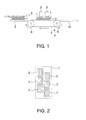
- Fig. 1 is a diagram schematically illustrating the configuration of an ink jet printer according to this embodiment.
- the ink jet printer shown in Fig. 1 is a line head type ink jet printer in which a printing medium 1 is transported in the arrow direction from the left to the right in the drawing and is subjected to a printing operation in a print area of a transport line.
- reference numeral 2 represents plural ink jet heads disposed above the transport line of the printing medium 1.
- the ink jet heads are arranged along a direction intersecting the printing medium transport direction so as to form two lines in the printing medium transport direction, and are fixed to a head fixing plate 7.
- Plural nozzles are formed in the bottom surface of each ink jet head 2 and thus the bottom surface is called a nozzle surface.
- the nozzles are arranged in a line in the direction intersecting the printing medium transport direction for each color of ink to be ejected, and thus the line is called a nozzle line or the line direction is called a nozzle line direction.
- the nozzle lines of the ink jet heads 2 arranged in the direction intersecting the printing medium transport direction form a line head covering the entire width in the direction intersecting the transport direction of the printing medium 1.
- the ink jet heads 2 are supplied with four colors of ink of yellow (Y), magenta (M), cyan (C), and black (K) from ink tanks not shown via ink supply tubes.
- the ink is simultaneously ejected to a predetermined position by a necessary amount from the nozzles formed in the ink jet heads 2, thereby forming a fine dot on the printing medium 1.
- a one-pass printing operation can be performed by passing the printing medium 1 transported by a transport unit 4 only once.
- a piezoelectric method is used as a method of ejecting ink from the nozzles of the ink jet heads 2.
- the piezoelectric method when a drive signal is applied to a piezoelectric element as an actuator, a vibration membrane in a pressure chamber is displaced to vary the volume of the pressure chamber and ink in the pressure chamber is ejected from the nozzles by means of the variation in pressure resulting therefrom.
- the amount of ink to be ejected can be adjusted by adjusting the crest value of the drive signal or the voltage change slope.
- the invention can be similarly applied to an ink ejecting method other than the piezoelectric method.
- a transport unit 4 transporting the printing medium 1 in a transport direction is disposed below the ink jet heads 2.
- a transport belt 6 is wound on a driving roller 8 and a driven roller 9 and an electric motor not shown is connected to the driving roller 8.
- a suction unit (not shown) suctioning the printing medium 1 onto the surface of the transport belt 6 is disposed on the inside of the transport belt 6. Examples of the suction unit include a vacuum suction unit suctioning the printing medium 1 onto the transport belt 6 using a negative pressure and an electrostatic suction unit suctioning the printing medium 1 onto the transport belt 6 using an electrostatic force.
- the transport belt 6 rotates in the printing medium transport direction and the printing medium 1 is suctioned onto the transport belt 6 by the suction unit and is then transported.
- ink is ejected from the ink jet heads 2 to perform a printing operation.
- the printing medium 1 having been subjected to the printing operation is discharged to a sheet discharge unit 10 downstream in the transport direction.
- a print reference signal output unit including, for example, a linear encoder is disposed in the transport belt 6, and ink of a predetermined color is ejected to a predetermined position on the printing medium 1 to form a dot by outputting a drive signal to the actuator from a driver to be described later on the basis of a pulse signal corresponding to a requested resolution and being output from the print reference signal output unit, whereby a predetermined image is drawn on the printing medium 1 by the use of the dots.
- a print reference signal output unit including, for example, a linear encoder is disposed in the transport belt 6, and ink of a predetermined color is ejected to a predetermined position on the printing medium 1 to form a dot by outputting a drive signal to the actuator from a driver to be described later on the basis of a pulse signal corresponding to a requested resolution and being output from the print reference signal output unit, whereby a predetermined image is drawn on the printing medium 1 by the use of the dots.
- the ink jet printer is provided with a control unit 11 controlling the ink jet printer.
- the configuration of the control unit 11 is shown in Fig. 3 .
- print data input from a host computer 12 is read.
- the control unit includes a controller 13 constructed by a computer system performing various processes such as a printing process on the basis of the print data, a feed roller motor driver 15 controlling the driving of a feed roller motor 14 connected to the feed roller 5, a head driver 16 controlling the driving of the ink jet heads 2, and an electric motor driver 18 controlling the driving of the electric motor 17 connected to the driving roller 8.
- the controller 13 includes a CPU (Central Processing Unit) 13a, a Ram (Random Access Memory) 13b, and a ROM (Read Only Memory) 13c.
- the CPU 13a performs various processes such as a printing process
- the RAM 13b temporarily stores the input print data or various data used to perform the print data printing process or temporarily develops programs of the printing process and the like.
- the ROM 13c includes a nonvolatile semiconductor memory storing a control program to be executed by the CPU 13a.
- the controller 13 When the controller 13 receives print data (image data) from the host computer 12, the CPU 13a performs a predetermined process on the print data and calculates nozzle selection data (drive pulse selection data) indicating which nozzles are to eject ink or and what amount of ink is to be ejected.
- the controller outputs a control signal and a drive signal to the feed roller motor driver 15, the head driver 16, and the electric motor driver 18 on the basis of the print data, the drive pulse selection data, and input data from various sensors.
- the feed roller motor 14, the electric motor 17, and the actuators in the ink jet heads 2 work, whereby the processes of feeding, transporting, and discharging the printing medium 1 and the process of performing a printing process on the printing medium 1 are carried out.
- the elements of the controller 13 are electrically connected to each other via a bus not shown.
- Fig. 4 shows an example of a drive signal COM being supplied to the ink jet heads 2 from the head driver 16 of the control unit 11 and being used to drive the actuators including piezoelectric elements.
- the drive signal is a signal in which a voltage varies about a middle voltage.
- the drive signal COM is formed by connecting drive pulses PCOM as a unit drive signal used to drive the actuators to eject ink in time series. At the rising edge of each drive pulse PCOM, the volume of the pressure chamber communicating with the nozzles is enlarged to intrude the ink therein. At the falling edge of each drive pulse PCOM, the volume of the pressure chamber is reduced to extrude the ink therefrom. By extruding the ink, the ink is ejected from the nozzles.
- the drive pulse PCOM1 on the leftmost side in Fig. 4 only intrudes the ink therein but does not extrude the ink. This is called micro vibration, which is used not to eject ink but to suppress or prevent thickening of the nozzles.
- drive pulse selection data SI In addition to the drive signal COM, drive pulse selection data SI, a latch signal LAT, a channel signal CH, and a clock signal SCK used to transmit the drive pulse selection data SI as a serial signal to the ink jet heads 2 are input as the control signal to the ink jet heads 2 from the control unit shown in Fig. 3 .
- the drive pulse selection data SI is data indicating what drive pulse PCOM to select from the drive pulses PCOM on the basis of the print data.
- the latch signal LAT and the channel signal CH connect the drive signal COM to the actuators of the ink jet heads 2 on the basis of the drive pulse selection data SI after inputting the nozzle selection data to all the nozzles.
- the minimum unit of the drive signal for driving the actuators 19 is referred to as the drive pulse PCOM and the signal in which the drive pulses PCOM are connected in time series is referred to as the drive signal COM. That is, a series of drive signals COM is output in response to the latch signal LAT and the drive pulse PCOM is output for each channel signal CH.
- Fig. 5 shows the specific configuration of a switching controller built in the ink jet heads 2 so as to supply the drive signal COM (drive pulses PCOM) to the actuators 19.
- the switching controller includes a register 20, a latch circuit 21 temporarily storing data of the register 20, and a level shifter 22 connecting the drive signal COM (drive pulses PCOM) to the actuators 19 including a piezoelectric element by converting the level of the output of the latch circuit 21 and supplying the converted signal to a selection switch 23.
- the register 20 stores the drive pulse selection data SI for selecting the actuator 19 of a piezoelectric element corresponding to the nozzle ejecting the ink.
- the level shifter 22 converts the output of the latch circuit into a voltage level capable of turning on or off the selection switch 23. This is because the drive signal COM (drive pulses PCOM) is higher than the output voltage of the latch circuit 21 and thus the operation voltage range of the selection switch 23 is set to be high. Therefore, the actuators 19 of which the selection switch 23 is turned on by the level shifter 22 is connected to the drive signal COM (drive pulses PCOM) at a predetermined connection time on the basis of the drive pulse selection data SI. After the drive pulse selection data SI of the register 20 is stored in the latch circuit 21, next print information is input to the register 20 and the data stored in the latch circuit 21 is sequentially updated at the time of ejecting ink.
- drive pulse selection data SI of the register 20 is stored in the latch circuit 21
- next print information is input to the register 20 and the data stored in the latch circuit 21 is sequentially updated at the time of ejecting ink.
- Reference sign HGND in the drawing represents a ground terminal of the actuators 19 including a piezoelectric element. Even after the actuator 19 of a piezoelectric element is disconnected from the drive signal COM (drive pulses PCOM) by the selection switch 23 (after the selection switch 23 is turned off), the input voltage of the corresponding actuator 19 is maintained at the voltage just before the disconnection. That is, the actuators 19 including a piezoelectric element are capacitive loads.
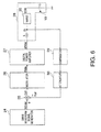
- Fig. 6 schematically shows the configuration of a driving circuit of the actuators 19.
- the driving circuit of the actuators is constructed in the head driver 16 of the control unit 11.
- the driving circuit includes a drive waveform signal generator 24, a subtractor 25, a modulator 26, a digital power amplifier 27, a smoothing filter 28, and a compensator 29 and an attenuator 30 inserted into a feedback circuit to the subtractor 25.
- the drive waveform signal generator 24 generates a drive waveform signal WCOM serving as a source of the drive signal COM (drive pulses PCOM), that is, a reference of a signal used to control the driving of the actuator 19, on the basis of drive waveform data DWCOM stored in advance.
- WCOM drive pulses PCOM
- the subtractor 25 subtracts a feedback signal Ref from the drive waveform signal WCOM generated by the drive waveform signal generator 24 and outputs a differential signal Diff.
- the modulator 26 pulse-modulates the differential signal Diff output from the subtractor 25.
- the digital power amplifier 27 power-amplifies the modulated signal PWM modulated by the modulator 26.
- the smoothing filter 28 smoothes the power-amplified modulated signal APWM power-amplified by the digital power amplifier 27 and outputs the smoothed signal as a drive signal COM to the actuators 19 including a piezoelectric element.
- the drive waveform signal generator 24 converts drive waveform data DWCOM including digital data into voltage signals and outputs the voltage signals after holding the resultant signals for a predetermined number of sampling periods.
- the subtractor 25 is a known analog subtraction circuit into which a resistor for a proportional constant is inserted.
- the modulator 26 employs a known pulse-width modulation (PWM) circuit.
- PWM pulse-width modulation
- the pulse-width modulation circuit includes a triangular wave oscillator 31 outputting a triangular-wave signal of a predetermined frequency and a comparator 32 comparing the triangular-wave signal with the differential signal Diff and outputting a modulated signal PWM with a pulse duty which is in an ON-duty state, for example, when the differential signal Diff is greater than the triangular-wave signal.
- the modulator 26 may employ a known pulse-modulation circuit such as a pulse density modulation (PDM) circuit.
- PDM pulse density modulation
- the operating voltage range of the subtractor 25 employing the analog subtraction circuit is 0 to 5 V.
- the digital power amplifier 27 includes a half-bridge output terminal 33 including a high-side switching element Q1 and a low-side switching element Q2 so as to actually amplify power and a gate drive circuit 34 adjusting gate-source signals GH and GL of the high-side switching element Q1 and the low-side switching element Q2 on the basis of the modulated signal PWM from the modulator 26.
- the gate-source signal GH of the high-side switching element Q1 and the gate-source signal GL of the low-side switching element Q2 when the modulated signal is at a high level. Accordingly, the high-side switching element Q1 is turned on and the low-side switching element Q2 is turned off.
- the output voltage Va of the half-bridge output terminal 33 is equal to a supply voltage VDD.
- the modulated signal is at a low level
- the gate-source signal GH of the high-side switching element Q1 becomes the low level
- the gate-source signal GL of the low-side switching element Q2 becomes the high level. Accordingly, the high-side switching element Q1 is turned off and the low-side switching element Q2 is turned on. As a result, the output voltage Va of the half-bridge output terminal 33 becomes 0.
- the loss itself of the digital power amplifier 27 is very small and can employ a switching element such as a small-sized MOSFET.
- the smoothing filter 28 includes an inductor L, an actuator 19 including a piezoelectric element as a capacitive load, and a wire 35 to form a secondary low-pass filter.
- the wire 35 including board interconnections is necessary between the control unit 11 and the ink jet heads 2.
- the smoothing filter 28 since the wire 35 generally has a resistance component and an inductance component, the smoothing filter 28 according to this embodiment constitutes a secondary low-pass filter including the inductance component of the inductor L, the resistance component and the inductance component of the wire, and the capacitance component of the actuator 19.
- the signal amplitude of the modulation frequency, that is, the pulse-modulation frequency, generated in the modulator 26 is attenuated and removed by the smoothing filter 28 and the drive signal COM (drive pulses PCOM) is output to the actuator 19.
- the drive signal to finally be output is ideally fed back.
- individually wires are necessary for feeding back the drive signal COM (drive pulses PCOM) to the actuator 19, which is not realistic. Therefore, in this embodiment, an inductor output signal SL is extracted from the connecting point between the inductor L of the smoothing filter 28 and the wire 35 and is fed back to the feedback circuit.
- the compensator 29 and the attenuator 30 are inserted into the feedback circuit. In this embodiment, as shown in Fig.
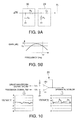
- a primary high-pass filter including a capacitor C 1 and a resistor R 1 is employed as the compensator 29, and a primary low-pass filter including a resistor R 2 and a capacitor C 2 is employed as the attenuator 30.
- the high-pass filter has a phase-preceding characteristic and thus can compensate for the feedback signal by causing the phase of the feedback signal Ref to precede using this characteristic.
- the phase-preceding characteristic is also referred to as a differential characteristic.
- the low-pass filter has a phase-lag characteristic.
- the phase-lag characteristic is also referred to as an integral characteristic.
- the feedback circuit including the combination of the compensator 29 employing the high-pass filter and the attenuator 30 employing the low-pass filter has the frequency characteristic shown in Fig. 9B . Particularly, a predetermined negative gain -y A is obtained in the modulation frequency or the modulation frequency band f car by the attenuator 30.
- Fig. 10 shows an example of the feedback signal Ref input to the subtractor 25 and the differential signal Diff output from the subtractor 25 (a typical drive waveform signal, not the drive waveform signal including the above-mentioned trapezoidal voltage signal, is shown in the drawing).
- the signal amplitude of a high frequency corresponding to the modulation frequency or the modulation frequency band f car of the feedback signal Ref is attenuated well.
- the differential signal Diff does not exceed the operating voltage range of 0 to 5 V of the subtractor 25.
- the differential signal Diff does not exceed the operating voltage range of the subtractor 25, it does not exceed the operating voltage range of the modulator 26 and thus the power-amplified modulated signal APWM which is the output signal of the digital power amplifier 27 and the drive signal COM (drive waveform signal PCOM) applied to the actuator 19 are also corrected, whereby the compensation using the feedback circuit is established.
- the power-amplified modulated signal APWM which is the output signal of the digital power amplifier 27 and the drive signal COM (drive waveform signal PCOM) applied to the actuator 19 are also corrected, whereby the compensation using the feedback circuit is established.
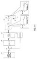
- Fig. 11 shows an example of a drive circuit and a feedback circuit according to the related art in which only the compensator 29 is inserted in to the feedback circuit, as described in JP-A-2007-96364 .
- a secondary low-pass filter including the inductance component of an inductor and the capacitance component of a capacitor is necessary as the smoothing filter 28, it is ideal in consideration of the stability of a system that the capacitor on the output side of the inductor L in the drawing is grounded and a dumping resistor is inserted before and after the inductor.
- the dumping resistor can be made to be unnecessary by feeding back the output signal using the capacitance component C of the actuator 19 instead of the capacitor.
- the driving circuit and the feedback circuit shown in Fig. 11 can be considered.
- the drive signal COM drive pulses PCOM
- the frequency characteristic in the connecting point between the actuator 19 and the wire 35 should be a predetermined negative gain -y in the modulation frequency or the modulation frequency band f car .
- the function of the smoothing filter 28 is not satisfactorily exhibited in the connecting point between the inductor L of the smoothing filter 28 and the wire 35 and the predetermined negative gain -y is not obtained in the modulation frequency or the modulation frequency band f car . Accordingly, the signal amplitude of the modulation frequency or the modulation frequency band f car may remain in the inductor output signal SL.
- Fig. 12A shows the feedback circuit of Fig. 11 .
- the frequency characteristic (which is the same as the frequency characteristic of the compensator 29 in this case) of the feedback circuit is that the gain in the modulation frequency or the modulation frequency band f car is 0, that is, is not attenuated at all. Accordingly, the signal amplitude of the modulation frequency or the modulation frequency band f car remains in the feedback signal Ref. For example, as shown in Fig.
- the differential signal Diff output from the subtractor 25 exceeds the operating voltage range of 0 to 5 V of the subtractor 25 and the differential signal Diff which should be inherently indicated by the two-dot chained line is cut off by the upper limit 5V of the operating voltage as indicated by the solid line and is thus distorted.
- the differential signal Diff is distorted, the modulated signal PWM and the power-amplified modulated signal APWM are also distorted and the drive signal COM (drive pulses PCOM) is thus distorted, whereby the compensation by the feedback circuit is not established.
- the compensation can be established by the combination of the compensator 29 causing the phase to precede and the attenuator 30 attenuating the signal amplitude of the modulation frequency or the modulation frequency band f car and the precision of the drive signal COM (drive pulses PCOM) can be guaranteed.
- the high-pass filter has a phase-preceding characteristic and the low-pass filter has a phase-lag characteristic.
- the high-pass filter is employed as the compensator 29 and the low-pass filter is employed as the attenuator 30, it is possible to set both transfer characteristics by setting constants and thus to finely adjust the frequency characteristic.
- Fig. 14A shows an equivalent circuit of the actuator driving circuit shown in Fig. 6 .
- an input signal x corresponds to the drive waveform signal WCOM and the output signal y 1 corresponds to the drive signal COM (drive pulses PCOM).
- An output signal y 2 corresponds to the inductor output signal SL and an output signal y 3 corresponds to the feedback signal Ref.
- the transfer function of the smoothing filter 28 is H 2
- the gain from the modulator 26 to the digital power amplifier 27 is A
- the transfer function of the compensator 29 is ⁇
- the transfer function of the attenuator 30 is ⁇ .
- Fig. 14B shows an equivalent circuit of from the wire 35 to the actuator 19, where the transfer function of the equivalent circuit is H 1 .
- Expression (5) can be obtained by expressing the output signal y 2 by the transfer function Gy 2 , and the output signal y 3 in response to the input signal x, that is, the transfer function Gy 3 of the feedback signal Ref, is expressed by Expression (6).
- y 3 ⁇ ⁇ ⁇ ⁇ y 2 ... 4
- Expression (8) can be obtained from Expression (7).
- the transfer function Gy 2 of the output signal y 2 in response to the input signal x is expressed by Expression (9).
- y 2 A ⁇ H 2 ⁇ x - ⁇ ⁇ ⁇ ⁇ y 2 ... 7
- y 3 1 ⁇ ⁇ ⁇ + 1 A ⁇ H 2 ⁇ x ... 8
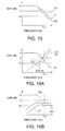
- Fig. 15 shows an example of the output signal y 1 the in response to the input signal x, that is, transfer function Gy 1 of the drive signal COM (drive pulses PCOM), and the transfer function H 1 from the wire 35 to the actuator 19.
- the transfer function Gy 1 is a target value and also a designed value.
- the transfer function H 1 is a predetermined value. Accordingly, the output signal y 2 in response to the input signal x, that is, the transfer function Gy 2 of the inductor output signal SL, is the same as indicated by the broken line in the drawing.
- the feedback from the smoothing filter 28 employing the secondary low-pass filter is performed to remove the resonance peak from the characteristic of the output signal y 1 in response to the input signal x, that is, the transfer function Gy 1 of the drive signal COM (drive pulses PCOM).
- the transfer characteristic (gain) ⁇ of the compensator 29 is set to remove the resonance peak from the characteristic of the transfer function Gy 1 .
- the transfer characteristic (gain) ⁇ of the attenuator 30 can be first set to 1.
- the transfer characteristic (gain) ⁇ of the compensator 29 is set by adding ⁇ /H 1 to the transfer function of the reciprocal of A ⁇ H 1 ⁇ H 2 having the resonance characteristic to cancel the resonance peak of 1/Gy 1 , as shown in Fig. 16A .
- the amount of attenuated amplitude of the modulation frequency component is considered with reference to the output of the digital power amplifier.
- the gain of the modulation frequency component as viewed from the input x is the output A (dB) of the digital power amplifier and the gain of the modulation frequency component after the attenuator 30 as viewed from the input x is -y s (dB). That is, the gain of the modulation frequency component varies from A (dB) to -y s (dB) and the amount of attenuated amplitude of the modulation frequency or the modulation frequency band f car is A+y s (dB).
- the amount of attenuated amplitude A+y s (dB) of the modulation frequency or the modulation frequency band f car in the feedback signal Ref is set so as not to exceed the operating voltage range (the range of 0 to 5 V in this embodiment) of a so-called analog signal system such as the subtractor 25 or the modulator 26.
- the transfer characteristic (gain) ⁇ of the attenuator 30 is set so that the amount of attenuated signal amplitude of the modulation frequency or the modulation frequency band f car in the output signal y 3 in response to the input signal x, that is, the transfer function Gy 3 of the feedback signal Ref, is equal to or less than A+y s (dB).
- the drive signal COM drive pulses PCOM
- the volume of the pressure chamber of each ink jet head 2 is reduced to eject ink in the pressure chamber.
- the inductor L is connected to the actuator 19 employing a capacitive load with the wire 35 to constitute the smoothing filter 28, and the inductor output signal SL output from the connecting point between the inductor L and the wire 35 is made to pass through the compensator 29 and the attenuator 30 and is then used as the feedback signal Ref to the subtractor 25.
- the attenuator 30 By setting the attenuator 30 to attenuate the feedback signal Ref so that the signal amplitude do not exceed the operating voltage range of at least one of the subtractor 25 and the modulator 26, it is possible to satisfactorily prevent the signal amplitude of the modulation frequency band f car exceeding the operating voltage range of the subtractor 25 or the modulator 26 from remaining in the feedback signal Ref.
- the attenuator 30 having a phase-lag characteristic, it is possible to remove the distortion of the feedback signal Ref by the use of the integrating function of the phase-lag characteristic.
- the phase-lag characteristic of the attenuator 30 By adjusting the phase-lag characteristic of the attenuator 30 to adjust the frequency characteristic of the feedback circuit, it is possible to adjust the frequency characteristic of the drive signal COM (drive pulses PCOM).
- the capacitive load driving circuit according to the invention is applied to a line head type ink jet printer
- the capacitive load driving circuit according to the invention may be similarly applied to a multi-pass type ink jet printer.
- a capacitive load driving circuit according to a second embodiment of the invention will be described below.
- the same elements as described in the first embodiment are referenced by the same reference numerals and signs as described in the first embodiment and detailed description thereof will not be repeated.
- Fig. 17A is a block diagram illustrating an example of the compensator 29 and the attenuator 30 disposed in the feedback circuit according to this embodiment.
- the compensator 29 shown in this example employs a primary high-pass filter including a capacitor C 1 and a resistor R 1
- the attenuator 30 employs a voltage divider including a resistor R 3 inserted into the circuit and a resistor R 4 grounded on the output side thereof. Accordingly, the frequency characteristic of the feedback circuit shown in Fig.
- FIG. 17A can be illustrated as shown in Fig. 17B .
- Fig. 18A is a block diagram illustrating another example of the compensator 29 and the attenuator 30 disposed in the feedback circuit according to this embodiment.
- the compensator 29 shown in this example employs a primary high-pass filter including a capacitor C 1 and a resistor R 1
- the attenuator 30 employs a voltage divider including a resistor R 5 inserted into the circuit and a grounded resistor R 1 in the compensator 29. That is, the attenuator 30 is constructed by the combination with the compensator 29.
- the frequency characteristic of the feedback circuit shown in Fig. 18A can be illustrated as shown in Fig. 18B . In this embodiment, similarly to the Figs.
- Fig. 19 shows an example of the feedback signal Ref input to the subtractor 25 and the differential signal Diff output from the subtractor 25 according to this embodiment (a typical drive waveform signal, not the drive waveform signal including the above-mentioned trapezoidal voltage signal, is shown in the drawing).
- a typical drive waveform signal not the drive waveform signal including the above-mentioned trapezoidal voltage signal, is shown in the drawing.
- the signal amplitude of a high frequency corresponding to the modulation frequency or the modulation frequency band f car of the feedback signal Ref is attenuated well.
- the differential signal Diff does not exceed the operating voltage range of 0 to 5 V of the subtractor 25.
- the differential signal Diff does not exceed the operating voltage range of the subtractor 25, it does not exceed the operating voltage range of the modulator 26 and thus the power-amplified modulated signal APWM which is the output signal of the digital power amplifier 27 and the drive signal COM (drive waveform signal PCOM) applied to the actuator 19 are also corrected, whereby the compensation using the feedback circuit is established.
- the power-amplified modulated signal APWM which is the output signal of the digital power amplifier 27 and the drive signal COM (drive waveform signal PCOM) applied to the actuator 19 are also corrected, whereby the compensation using the feedback circuit is established.
- the capacitive load driving circuit according to this embodiment, it is possible to attenuate the signal amplitude of the high frequency corresponding to the modulation frequency or the modulation frequency band f car of the feedback signal Ref while removing the resonance peak from the transfer function characteristic of the drive signal.
- the differential signal Diff does not exceed the operating voltage range of 0 to 5 V of the subtractor 25, it is possible to establish the compensation using the feedback circuit.
- the attenuator includes one or more resistors, it is possible to remove the distortion of the feedback signal Ref with a simpler configuration.
- a capacitive load driving circuit according to a third embodiment of the invention will be described below.
- the same elements as described in the first embodiment are referenced by the same reference numerals and signs as described in the first embodiment and detailed description thereof will not be repeated.
- This embodiment is different from the first and second embodiments, in the configuration of the feedback circuit disposed in the actuator driving circuit. Similarly to the first and second embodiments, the feedback circuit includes the compensator 29 and the attenuator 30, but the specific configuration thereof is changed.
- Fig. 20A is a block diagram illustrating an example of the compensator 29 and the attenuator 30 disposed in the feedback circuit according to this embodiment.
- the compensator 29 and the attenuator 30 shown in the drawing employ a primary high-pass filter including a capacitor C 1 and a resistor R 1 and a primary low-pass filter including a resistor R 2 and a capacitor C 2 , respectively.
- a resistor R 6 is inserted into the input side of the high-pass filter constituting the compensator 29 to constitute the attenuator 30 employing a voltage divider including the resistor R 6 and the grounded resistor R 1 of the compensator 29.
- the frequency characteristic of the feedback circuit shown in Fig. 20A can be illustrated as shown in Fig. 20B and it is thus possible to further reduce the gain in the modulation frequency or the modulation frequency band f car into a predetermined negative gain -y D , compared with the feedback circuit according to the first embodiment shown in Figs. 9A and 9B .
- the actuator driving circuit according to this embodiment it is possible to variously set the attenuation characteristic of the attenuator 30.
- Fig. 21 shows an example of the feedback signal Ref input to the subtractor 25 and the differential signal Diff output from the subtractor 25 according to this embodiment (a typical drive waveform signal, not the drive waveform signal including the above-mentioned trapezoidal voltage signal, is shown in the drawing).
- a typical drive waveform signal not the drive waveform signal including the above-mentioned trapezoidal voltage signal, is shown in the drawing.
- the signal amplitude of a high frequency corresponding to the modulation frequency or the modulation frequency band f car of the feedback signal Ref is attenuated well.
- the differential signal Diff does not exceed the operating voltage range of 0 to 5 V of the subtractor 25.
- the differential signal Diff does not exceed the operating voltage range of the subtractor 25, it does not exceed the operating voltage range of the modulator 26 and thus the power-amplified modulated signal APWM which is the output signal of the digital power amplifier 27 and the drive signal COM (drive waveform signal PCOM) applied to the actuator 19 are also corrected well, whereby the compensation using the feedback circuit is established.
- the power-amplified modulated signal APWM which is the output signal of the digital power amplifier 27 and the drive signal COM (drive waveform signal PCOM) applied to the actuator 19 are also corrected well, whereby the compensation using the feedback circuit is established.
- the capacitive load driving circuit according to the invention is applied to the driving of actuators which are capacitive loads of an ink jet printer.
- the capacitive load driving circuit according to the invention may be similarly applied to the driving of a capacitive load used in a fluid ejecting apparatus.
- the fluid ejecting apparatus employing a capacitive load include a water pulse scalpel suitably installed in a distal end of a catheter which is inserted into a blood vessel to remove blood clots and the like and a water pulse scalpel suitable for incising or excising a biological tissue.
- the fluid used as the water pulse scalpel is water or physiological saline.
- the water pulse scalpel ejects a high-pressure liquid supplied from a pump as a pulse flow.
- a piezoelectric element as a capacitive load is driven to displace a diaphragm constituting a fluid chamber to generate the pulse flow.
- the piezoelectric element as a capacitive load and a fluid ejection controller controlling the piezoelectric element are disposed separately from each other. Accordingly, by applying the capacitive load driving circuit according to the invention to the water pulse scalpel, it is possible to guarantee the precision of the drive signal of the capacitive load, thereby ejecting a fluid with high precision.
- the fluid ejecting apparatus employing the capacitive load driving circuit according to the invention may be embodied as a fluid ejecting apparatus ejecting a liquid (including a liquid-like material in which functional material particles are dispersed and a fluidic material such as gel in addition to the liquid) other than the ink or the physiological saline or a fluid (including a solid which can be ejected as a fluid) other than the liquid.
- a liquid including a liquid-like material in which functional material particles are dispersed and a fluidic material such as gel in addition to the liquid
- a fluidic material such as gel in addition to the liquid
- Examples thereof include a liquid-like material ejecting apparatus ejecting a liquid-like material with dispersed or melted electrode materials or color materials which are used to produce, for example, a liquid crystal display, an EL (Electroluminescence) display, a surf ace emission display, and a color filter, a fluid ejecting apparatus ejecting biological organic materials used to produce a bio chip, and a fluid ejecting apparatus which is used as a precision pipette ejecting a liquid as a sample.
- a liquid-like material ejecting apparatus ejecting a liquid-like material with dispersed or melted electrode materials or color materials which are used to produce, for example, a liquid crystal display, an EL (Electroluminescence) display, a surf ace emission display, and a color filter
- a fluid ejecting apparatus ejecting biological organic materials used to produce a bio chip
- a fluid ejecting apparatus which is used as a precision pipette e
- Examples thereof also include a fluid ejecting apparatus ejecting lubricant to precision machinery such as watches and cameras with a pinpoint and a fluid ejecting apparatus ejecting a transparent resin solution of an ultraviolet-curable resin or the like on a substrate so as to form micro semi-spherical lenses (optical lenses) used for optical communication devices.
- Examples thereof further include a fluid ejecting apparatus ejecting an etchant of acid or alkali so as to etch a substrate and the like, a fluidic material ejecting apparatus ejecting gel, and a fluid-ejecting recording apparatus ejecting a solid such as toner powders.
- the invention may be applied to any type of ejecting apparatus thereof.
Landscapes
- Health & Medical Sciences (AREA)
- Engineering & Computer Science (AREA)
- Surgery (AREA)
- Life Sciences & Earth Sciences (AREA)
- Molecular Biology (AREA)
- Biomedical Technology (AREA)
- Heart & Thoracic Surgery (AREA)
- Medical Informatics (AREA)
- Nuclear Medicine, Radiotherapy & Molecular Imaging (AREA)
- Animal Behavior & Ethology (AREA)
- General Health & Medical Sciences (AREA)
- Public Health (AREA)
- Veterinary Medicine (AREA)
- Microelectronics & Electronic Packaging (AREA)
- Particle Formation And Scattering Control In Inkjet Printers (AREA)
- Surgical Instruments (AREA)
Abstract
Description
- The present invention relates to a capacitive load driving circuit that supplies a drive signal to a capacitive load such as a piezoelectric element so as to drive the capacitive load, and more particularly, to an ink jet printer that includes an actuator as a capacitive load and that performs a printing operation by supplying a drive signal to the actuator so as to eject ink or a fluid ejecting apparatus that includes an actuator such as a capacitive load connected to a diaphragm and supplies a drive signal to the actuator so as to eject fluid.
- For example, when a drive waveform signal having a predetermined voltage waveform is amplified by a digital power amplifier and is used as a drive signal of an actuator which is a capacitive load, the drive waveform signal is pulse-modulated into a modulated signal by the use of a modulator, the modulated signal is amplified in power into a power-amplified modulated signal by the use of the digital power amplifier, and the power-amplified modulated signal is smoothed into a drive signal by the use of a smoothing filter.
- When the waveform of the drive signal is important, the drive signal may be made to precede in phase into a feedback signal and a differential value between the feedback signal and the drive waveform signal obtained from a subtractor may be input to the modulator. For example, in
JP-A-2007-96364 - When an actuator as a capacitive load is separated from a digital power amplifier, a wire in addition to a substrate interconnection is necessary between the actuator and the digital power amplifier. In this case, it is not realistic that the drive signal actually supplied to the actuator is fed back, because an individual wire is necessary and the like. Accordingly, for example, an inductor is disposed at an output terminal of the digital power amplifier and a signal at a connecting point between the inductor and the wire is fed back. However, when the input signal to the wire is fed back, signal amplitude in a modulation frequency band exceeding an operating range of the subtractor or the modulator may remain in a feedback signal only by inserting the phase-preceding compensator into the feedback circuit. In this case, there is a problem in that it is not possible to satisfactorily compensate for the drive signal.
- An advantage of some aspects of the invention is that it provides a capacitive load driving circuit, an ink jet printer, and a fluid ejecting apparatus, which can prevent signal amplitude in a modulation frequency band exceeding an operating range of a subtractor or a modulator from remaining in a feedback signal.
- According to an aspect of the invention, there is provided a capacitive load driving circuit including: a drive waveform signal generator that generates a drive waveform signal; a subtractor that outputs a differential signal between the drive waveform signal and a feedback signal; a modulator that pulse-modulates the differential signal and outputs a modulated signal; a digital power amplifier that amplifies the power of the modulated signal and outputs a power-amplified modulated signal; a smoothing filter that is constructed by connecting an inductor and a capacitive load with a wire, smoothes the power-amplified modulated signal, and outputs a drive signal of the capacitive load; a compensator that causes a phase to precede the drive signal; and an attenuator that attenuates signal amplitude in a band at least including a modulation frequency of the modulated signal. Here, a signal output from a connecting point between the inductor and the wire is made to pass through the compensator and the attenuator and is then used as a feedback signal to the subtractor.
- According to this capacitive load driving circuit, for example, when a wire is necessarily disposed between the capacitive load of the actuator and the digital power amplifier, the inductor and the capacitive load are connected with the wire to form a smoothing filter and the signal output from the connecting point between the inductor and the wire is made to pass through the compensator and the attenuator and is then used as a feedback signal to the subtractor. Accordingly, it is possible to attenuate the signal amplitude in a modulation frequency band of the feed back signal by the use of the attenuator while removing the resonance peak from a transfer function characteristic of the drive signal. As a result, it is possible to prevent the signal amplitude in the modulation frequency band exceeding the operating range of the subtractor or the modulator from remaining in the feedback signal while compensating for the waveform of the drive signal, and to guarantee the precision of the drive signal.
- In the capacitive load driving circuit, the compensator may include a capacitor and a resistor, and the attenuator may be configured to include the resistor of the compensator.
- According to this capacitive load driving circuit, it is possible to simplify the circuit configuration and to set the attenuation characteristic of the attenuator to various values.
- In the capacitive load driving circuit, the attenuator may attenuate the signal amplitude so as not to exceed an allowable operating range of at least one of the subtractor and the modulator.
- According to this capacitive load driving circuit, it is possible to more satisfactorily prevent the signal amplitude in the modulation frequency band exceeding the operating range of the subtractor or the modulator from remaining in the feedback signal.
- In the capacitive load driving circuit, the attenuator may have a phase-lag characteristic.
- According to this capacitive load driving circuit, it is possible to remove the distortion of the feedback signal by the use of an integration function based on the phase-lag characteristic.
- In the capacitive load driving circuit, the attenuator may include one or more resistors.
- According to this capacitive load driving circuit, it is possible to remove the distortion of the feedback signal with a simpler configuration.
- In the capacitive load driving circuit, the attenuator may include a plurality of attenuators.
- According to this capacitive load driving circuit, it is possible to more satisfactorily remove the distortion of the feedback signal.
- According to another aspect of the invention, there is provided an ink jet printer having a plurality of actuators as a capacitive load in an ink jet head, applying a drive signal to the actuators so as to reduce a volume of a pressure chamber and to eject ink in the pressure chamber, performing a printing operation on a printing medium with the ejected ink, the ink jet printer including: a drive waveform signal generator that generates a drive waveform signal; a subtractor that outputs a differential signal between the drive waveform signal and a feedback signal; a modulator that modulates the differential signal and outputs a modulated signal; a digital power amplifier that amplifies the power of the modulated signal and outputs a power-amplified modulated signal; a smoothing filter that is constructed by connecting an inductor and the actuators with a wire, smoothes the power-amplified modulated signal, and outputs the drive signal; a compensator that causes a phase to precede the drive signal; and an attenuator that attenuates signal amplitude in a band at least including a carrier frequency of the modulated signal singly or in combination with the compensator. Here, a signal output from a connecting point between the inductor and the wire is made to pass through the compensator and the attenuator and is then used as a feedback signal to the subtractor.
- According to this ink jet printer, when the drive signal is applied to the actuator as a capacitive load, the volume of the pressure chamber of the ink jet head is reduced to eject ink in the pressure chamber and a printing operation is performed on a printing medium with the ejected ink. At this time, the inductor and the actuator as the capacitive load are connected with the wire to form the smoothing filter and the signal output from the connecting point between the inductor and the wire is made to pass through the compensator and the attenuator and is then used as a feedback signal to the subtractor. Accordingly, it is possible to attenuate the signal amplitude in a modulation frequency band of the feed back signal by the use of the attenuator while removing the resonance peak from a transfer function characteristic of the drive signal. As a result, it is possible to prevent the signal amplitude in the modulation frequency band exceeding the operating range of the subtractor or the modulator from remaining in the feedback signal while compensating for the waveform of the drive signal, and to guarantee the precision of the drive signal, thereby performing a printing operation with higher precision.
- According to still another aspect of the invention, there is provided a fluid ejecting apparatus having a plurality of actuators as a capacitive load connected to a diaphragm and applying a drive signal to the actuators so as to reduce a volume of a fluid chamber by means of the diaphragm and to eject fluid in the fluid chamber, the fluid ejecting apparatus including: a drive waveform signal generator that generates a drive waveform signal; a subtractor that outputs a differential signal between the drive waveform signal and a feedback signal; a modulator that modulates the differential signal and outputs a modulated signal; a digital power amplifier that amplifies the power of the modulated signal and outputs a power-amplified modulated signal; a smoothing filter that is constructed by connecting an inductor and the actuators with a wire, smoothes the power-amplified modulated signal, and outputs the drive signal; a compensator that causes a phase to precede the drive signal; and an attenuator that attenuates signal amplitude in a band at least including a carrier frequency of the modulated signal singly or in combination with the compensator. Here, a signal output from a connecting point between the inductor and the wire is made to pass through the compensator and the attenuator and is then used as a feedback signal to the subtractor.
- According to this fluid ejecting apparatus, when the drive signal is applied to the actuator as a capacitive load, the volume of the fluid chamber is reduced by means of the diaphragm to eject fluid in the fluid chamber. At this time, the inductor and the actuator as the capacitive load are connected with the wire to form the smoothing filter and the signal output from the connecting point between the inductor and the wire is made to pass through the compensator and the attenuator and is then used as a feedback signal to the subtractor. Accordingly, it is possible to attenuate the signal amplitude in a modulation frequency band of the feed back signal by the use of the attenuator while removing the resonance peak from a transfer function characteristic of the drive signal. As a result, it is possible to prevent the signal amplitude in the modulation frequency band exceeding the operating range of the subtractor or the modulator from remaining in the feedback signal while compensating for the waveform of the drive signal, and to guarantee the precision of the drive signal, thereby ejecting the fluid with higher precision.
- The invention will be described with reference to the accompanying drawings, wherein like numbers reference like elements.
-
Fig. 1 is a front view schematically illustrating the configuration of an ink jet printer employing a capacitive load driving circuit according to a first embodiment of the invention. -
Fig. 2 is a plan view illustrating the surrounding of an ink jet head used in the ink jet printer shown inFig. 1 . -
Fig. 3 is a block diagram illustrating the configuration of a control unit of the ink jet printer shown inFig. 1 . -
Fig. 4 is a diagram illustrating a drive signal of an actuator which is a capacitive load. -
Fig. 5 is a block diagram illustrating a switching controller. -
Fig. 6 is a block diagram illustrating a driver of an actuator. -
Fig. 7 is a block diagram illustrating a modulator shown inFig. 6 . -
Fig. 8 is a block diagram illustrating a digital power amplifier shown inFig. 6 . -
Figs. 9A and 9B are diagrams illustrating a feedback circuit shown inFig. 6 , whereFig. 9A is a block diagram andFig. 9B is a diagram illustrating a frequency characteristic. -
Fig. 10 is a diagram illustrating input and output signals of a subtractor shown inFig. 6 . -
Fig. 11 is a block diagram illustrating a driver of an actuator and a feedback circuit according to the related art. -
Figs. 12A and 12B are diagrams illustrating a feedback circuit shown inFig. 11 , whereFig. 12A is a block diagram andFig. 12B is a diagram illustrating a frequency characteristic. -
Fig. 13 is a diagram illustrating input and output signals of a subtractor shown inFig. 11 . -
Figs. 14A and 14B are diagrams illustrating an equivalent circuit of the driver of the actuator shown inFig. 6 . -
Fig. 15 is a diagram illustrating a frequency characteristic of the circuit shown inFigs. 14A and 14B . -
Figs. 16A and 16B are diagrams illustrating a frequency characteristic of the circuit shown inFigs. 14A and 14B . -
Figs. 17A and 17B are diagrams illustrating an example of a feedback circuit disposed in the actuator driver show inFig. 3 , whereFig. 17A is a block diagram andFig. 17B is a diagram illustrating a frequency characteristic. -
Figs. 18A and 18B are diagrams illustrating another example of the feedback circuit disposed in the actuator driver shown inFig. 3 , whereFig. 17A is a block diagram andFig. 17B is a diagram illustrating a frequency characteristic. -
Fig. 19 is a diagram illustrating input and output signals of the subtractor disposed in the actuator driver shown inFig. 3 . -
Figs. 20A and 20B are diagrams illustrating the feedback circuit disposed in the actuator driver shown inFig. 3 , whereFig. 20A is a block diagram andFig. 20B is a diagram illustrating a frequency characteristic. -
Fig. 21 is a diagram illustrating input and output signals of the subtractor disposed in the actuator driver shown inFig. 3 . - Hereinafter, a capacitive load driving circuit according to a first embodiment of the invention which is applied to an ink jet printer will be described.
-
Fig. 1 is a diagram schematically illustrating the configuration of an ink jet printer according to this embodiment. The ink jet printer shown inFig. 1 is a line head type ink jet printer in which aprinting medium 1 is transported in the arrow direction from the left to the right in the drawing and is subjected to a printing operation in a print area of a transport line. - In
Fig. 1 ,reference numeral 2 represents plural ink jet heads disposed above the transport line of theprinting medium 1. The ink jet heads are arranged along a direction intersecting the printing medium transport direction so as to form two lines in the printing medium transport direction, and are fixed to ahead fixing plate 7. Plural nozzles are formed in the bottom surface of eachink jet head 2 and thus the bottom surface is called a nozzle surface. As shown inFig. 2 , the nozzles are arranged in a line in the direction intersecting the printing medium transport direction for each color of ink to be ejected, and thus the line is called a nozzle line or the line direction is called a nozzle line direction. The nozzle lines of the ink jet heads 2 arranged in the direction intersecting the printing medium transport direction form a line head covering the entire width in the direction intersecting the transport direction of theprinting medium 1. - The ink jet heads 2 are supplied with four colors of ink of yellow (Y), magenta (M), cyan (C), and black (K) from ink tanks not shown via ink supply tubes. The ink is simultaneously ejected to a predetermined position by a necessary amount from the nozzles formed in the ink jet heads 2, thereby forming a fine dot on the
printing medium 1. By performing this operation for each color, a one-pass printing operation can be performed by passing theprinting medium 1 transported by atransport unit 4 only once. In this embodiment, a piezoelectric method is used as a method of ejecting ink from the nozzles of the ink jet heads 2. In the piezoelectric method, when a drive signal is applied to a piezoelectric element as an actuator, a vibration membrane in a pressure chamber is displaced to vary the volume of the pressure chamber and ink in the pressure chamber is ejected from the nozzles by means of the variation in pressure resulting therefrom. The amount of ink to be ejected can be adjusted by adjusting the crest value of the drive signal or the voltage change slope. The invention can be similarly applied to an ink ejecting method other than the piezoelectric method. - A
transport unit 4 transporting theprinting medium 1 in a transport direction is disposed below the ink jet heads 2. In thetransport unit 4, atransport belt 6 is wound on a drivingroller 8 and a drivenroller 9 and an electric motor not shown is connected to the drivingroller 8. A suction unit (not shown) suctioning theprinting medium 1 onto the surface of thetransport belt 6 is disposed on the inside of thetransport belt 6. Examples of the suction unit include a vacuum suction unit suctioning theprinting medium 1 onto thetransport belt 6 using a negative pressure and an electrostatic suction unit suctioning theprinting medium 1 onto thetransport belt 6 using an electrostatic force. Accordingly, when a sheet of theprinting medium 1 is fed to thetransport belt 6 from asheet feed unit 3 by afeed roller 5 and the drivingroller 8 is rotationally driven by the electric motor, thetransport belt 6 rotates in the printing medium transport direction and theprinting medium 1 is suctioned onto thetransport belt 6 by the suction unit and is then transported. In the course of transporting theprinting medium 1, ink is ejected from the ink jet heads 2 to perform a printing operation. Theprinting medium 1 having been subjected to the printing operation is discharged to asheet discharge unit 10 downstream in the transport direction. A print reference signal output unit including, for example, a linear encoder is disposed in thetransport belt 6, and ink of a predetermined color is ejected to a predetermined position on theprinting medium 1 to form a dot by outputting a drive signal to the actuator from a driver to be described later on the basis of a pulse signal corresponding to a requested resolution and being output from the print reference signal output unit, whereby a predetermined image is drawn on theprinting medium 1 by the use of the dots. - The ink jet printer according to this embodiment is provided with a
control unit 11 controlling the ink jet printer. The configuration of thecontrol unit 11 is shown inFig. 3 . First, print data input from ahost computer 12 is read. The control unit includes acontroller 13 constructed by a computer system performing various processes such as a printing process on the basis of the print data, a feedroller motor driver 15 controlling the driving of afeed roller motor 14 connected to thefeed roller 5, ahead driver 16 controlling the driving of the ink jet heads 2, and anelectric motor driver 18 controlling the driving of theelectric motor 17 connected to the drivingroller 8. - The
controller 13 includes a CPU (Central Processing Unit) 13a, a Ram (Random Access Memory) 13b, and a ROM (Read Only Memory) 13c. When theCPU 13a performs various processes such as a printing process, theRAM 13b temporarily stores the input print data or various data used to perform the print data printing process or temporarily develops programs of the printing process and the like. TheROM 13c includes a nonvolatile semiconductor memory storing a control program to be executed by theCPU 13a. When thecontroller 13 receives print data (image data) from thehost computer 12, theCPU 13a performs a predetermined process on the print data and calculates nozzle selection data (drive pulse selection data) indicating which nozzles are to eject ink or and what amount of ink is to be ejected. The controller outputs a control signal and a drive signal to the feedroller motor driver 15, thehead driver 16, and theelectric motor driver 18 on the basis of the print data, the drive pulse selection data, and input data from various sensors. In response to the control signal or the drive signal, thefeed roller motor 14, theelectric motor 17, and the actuators in the ink jet heads 2 work, whereby the processes of feeding, transporting, and discharging theprinting medium 1 and the process of performing a printing process on theprinting medium 1 are carried out. The elements of thecontroller 13 are electrically connected to each other via a bus not shown. -
Fig. 4 shows an example of a drive signal COM being supplied to the ink jet heads 2 from thehead driver 16 of thecontrol unit 11 and being used to drive the actuators including piezoelectric elements. In this embodiment, the drive signal is a signal in which a voltage varies about a middle voltage. The drive signal COM is formed by connecting drive pulses PCOM as a unit drive signal used to drive the actuators to eject ink in time series. At the rising edge of each drive pulse PCOM, the volume of the pressure chamber communicating with the nozzles is enlarged to intrude the ink therein. At the falling edge of each drive pulse PCOM, the volume of the pressure chamber is reduced to extrude the ink therefrom. By extruding the ink, the ink is ejected from the nozzles. - By variously changing the voltage change slope or the crest value of the drive pulse PCOM having a trapezoidal voltage waveform, an intrusion amount or intrusion rate of ink or an extrusion amount or an extrusion rate of ink can be changed and the amount of ink to be ejected can be accordingly changed, whereby different sizes of dots are formed. Therefore, even when plural drive pulses PCOM are connected in time series, various sizes of dots are obtained by selecting a single drive pulse PCOM therefrom and supplying the selected drive pulse to the
actuators 19 or selecting plural drive pulses PCOM and supplying the selected drive pulses to theactuators 19 and ejecting the ink plural times. That is, when plural ink droplets are landed onto the same position before the ink is dried, it is the same as actually ejecting a large size ink droplet, whereby the size of a dot can be enlarged. By combining such techniques, multi gray scales can be realized. The drive pulse PCOM1 on the leftmost side inFig. 4 only intrudes the ink therein but does not extrude the ink. This is called micro vibration, which is used not to eject ink but to suppress or prevent thickening of the nozzles. - In addition to the drive signal COM, drive pulse selection data SI, a latch signal LAT, a channel signal CH, and a clock signal SCK used to transmit the drive pulse selection data SI as a serial signal to the ink jet heads 2 are input as the control signal to the ink jet heads 2 from the control unit shown in
Fig. 3 . The drive pulse selection data SI is data indicating what drive pulse PCOM to select from the drive pulses PCOM on the basis of the print data. The latch signal LAT and the channel signal CH connect the drive signal COM to the actuators of the ink jet heads 2 on the basis of the drive pulse selection data SI after inputting the nozzle selection data to all the nozzles. Hereinafter, the minimum unit of the drive signal for driving theactuators 19 is referred to as the drive pulse PCOM and the signal in which the drive pulses PCOM are connected in time series is referred to as the drive signal COM. That is, a series of drive signals COM is output in response to the latch signal LAT and the drive pulse PCOM is output for each channel signal CH. -
Fig. 5 shows the specific configuration of a switching controller built in the ink jet heads 2 so as to supply the drive signal COM (drive pulses PCOM) to theactuators 19. The switching controller includes aregister 20, alatch circuit 21 temporarily storing data of theregister 20, and alevel shifter 22 connecting the drive signal COM (drive pulses PCOM) to theactuators 19 including a piezoelectric element by converting the level of the output of thelatch circuit 21 and supplying the converted signal to aselection switch 23. Theregister 20 stores the drive pulse selection data SI for selecting theactuator 19 of a piezoelectric element corresponding to the nozzle ejecting the ink. - The
level shifter 22 converts the output of the latch circuit into a voltage level capable of turning on or off theselection switch 23. This is because the drive signal COM (drive pulses PCOM) is higher than the output voltage of thelatch circuit 21 and thus the operation voltage range of theselection switch 23 is set to be high. Therefore, theactuators 19 of which theselection switch 23 is turned on by thelevel shifter 22 is connected to the drive signal COM (drive pulses PCOM) at a predetermined connection time on the basis of the drive pulse selection data SI. After the drive pulse selection data SI of theregister 20 is stored in thelatch circuit 21, next print information is input to theregister 20 and the data stored in thelatch circuit 21 is sequentially updated at the time of ejecting ink. Reference sign HGND in the drawing represents a ground terminal of theactuators 19 including a piezoelectric element. Even after theactuator 19 of a piezoelectric element is disconnected from the drive signal COM (drive pulses PCOM) by the selection switch 23 (after theselection switch 23 is turned off), the input voltage of the correspondingactuator 19 is maintained at the voltage just before the disconnection. That is, theactuators 19 including a piezoelectric element are capacitive loads. -
Fig. 6 schematically shows the configuration of a driving circuit of theactuators 19. The driving circuit of the actuators is constructed in thehead driver 16 of thecontrol unit 11. In this embodiment, the driving circuit includes a drivewaveform signal generator 24, asubtractor 25, amodulator 26, adigital power amplifier 27, a smoothingfilter 28, and acompensator 29 and anattenuator 30 inserted into a feedback circuit to thesubtractor 25. Here, the drivewaveform signal generator 24 generates a drive waveform signal WCOM serving as a source of the drive signal COM (drive pulses PCOM), that is, a reference of a signal used to control the driving of theactuator 19, on the basis of drive waveform data DWCOM stored in advance. Thesubtractor 25 subtracts a feedback signal Ref from the drive waveform signal WCOM generated by the drivewaveform signal generator 24 and outputs a differential signal Diff. Themodulator 26 pulse-modulates the differential signal Diff output from thesubtractor 25. Thedigital power amplifier 27 power-amplifies the modulated signal PWM modulated by themodulator 26. The smoothingfilter 28 smoothes the power-amplified modulated signal APWM power-amplified by thedigital power amplifier 27 and outputs the smoothed signal as a drive signal COM to theactuators 19 including a piezoelectric element. - The drive
waveform signal generator 24 converts drive waveform data DWCOM including digital data into voltage signals and outputs the voltage signals after holding the resultant signals for a predetermined number of sampling periods. Thesubtractor 25 is a known analog subtraction circuit into which a resistor for a proportional constant is inserted. As shown inFig. 7 , themodulator 26 employs a known pulse-width modulation (PWM) circuit. The pulse-width modulation circuit includes atriangular wave oscillator 31 outputting a triangular-wave signal of a predetermined frequency and acomparator 32 comparing the triangular-wave signal with the differential signal Diff and outputting a modulated signal PWM with a pulse duty which is in an ON-duty state, for example, when the differential signal Diff is greater than the triangular-wave signal. Themodulator 26 may employ a known pulse-modulation circuit such as a pulse density modulation (PDM) circuit. In this embodiment, the operating voltage range of thesubtractor 25 employing the analog subtraction circuit is 0 to 5 V. - As shown in
Fig. 8 , thedigital power amplifier 27 includes a half-bridge output terminal 33 including a high-side switching element Q1 and a low-side switching element Q2 so as to actually amplify power and agate drive circuit 34 adjusting gate-source signals GH and GL of the high-side switching element Q1 and the low-side switching element Q2 on the basis of the modulated signal PWM from themodulator 26. In thedigital power amplifier 27, the gate-source signal GH of the high-side switching element Q1 and the gate-source signal GL of the low-side switching element Q2 when the modulated signal is at a high level. Accordingly, the high-side switching element Q1 is turned on and the low-side switching element Q2 is turned off. As a result, the output voltage Va of the half-bridge output terminal 33 is equal to a supply voltage VDD. On the other hand, when the modulated signal is at a low level, the gate-source signal GH of the high-side switching element Q1 becomes the low level and the gate-source signal GL of the low-side switching element Q2 becomes the high level. Accordingly, the high-side switching element Q1 is turned off and the low-side switching element Q2 is turned on. As a result, the output voltage Va of the half-bridge output terminal 33 becomes 0. - When the high-side switching element Q1 and the low-side switching element Q2 are digitally driven in this way, a current flows in the turned-on switching element, but the drain-source resistance is very small and thus loss is almost zero. Since no current flows in the turned-off switching element, the loss is not generated. Therefore, the loss itself of the
digital power amplifier 27 is very small and can employ a switching element such as a small-sized MOSFET. - As shown in
Fig. 6 , the smoothingfilter 28 includes an inductor L, anactuator 19 including a piezoelectric element as a capacitive load, and awire 35 to form a secondary low-pass filter. In this embodiment, since plural ink jet heads 2 including theactuator 19 are disposed for thesingle control unit 11 and are separated from each other, thewire 35 including board interconnections is necessary between thecontrol unit 11 and the ink jet heads 2. Since thewire 35 generally has a resistance component and an inductance component, the smoothingfilter 28 according to this embodiment constitutes a secondary low-pass filter including the inductance component of the inductor L, the resistance component and the inductance component of the wire, and the capacitance component of theactuator 19. The signal amplitude of the modulation frequency, that is, the pulse-modulation frequency, generated in themodulator 26 is attenuated and removed by the smoothingfilter 28 and the drive signal COM (drive pulses PCOM) is output to theactuator 19. - As the feedback signal, the drive signal to finally be output is ideally fed back. However, when the
wire 35 is necessary between thecontrol unit 11 and theactuator 19 as in this embodiment, individually wires are necessary for feeding back the drive signal COM (drive pulses PCOM) to theactuator 19, which is not realistic. Therefore, in this embodiment, an inductor output signal SL is extracted from the connecting point between the inductor L of the smoothingfilter 28 and thewire 35 and is fed back to the feedback circuit. As described above, thecompensator 29 and theattenuator 30 are inserted into the feedback circuit. In this embodiment, as shown inFig. 9A , a primary high-pass filter including a capacitor C1 and a resistor R1 is employed as thecompensator 29, and a primary low-pass filter including a resistor R2 and a capacitor C2 is employed as theattenuator 30. As known widely, the high-pass filter has a phase-preceding characteristic and thus can compensate for the feedback signal by causing the phase of the feedback signal Ref to precede using this characteristic. The phase-preceding characteristic is also referred to as a differential characteristic. On the other hand, the low-pass filter has a phase-lag characteristic. The phase-lag characteristic is also referred to as an integral characteristic. - The feedback circuit including the combination of the
compensator 29 employing the high-pass filter and theattenuator 30 employing the low-pass filter has the frequency characteristic shown inFig. 9B . Particularly, a predetermined negative gain -yA is obtained in the modulation frequency or the modulation frequency band fcar by theattenuator 30. -
Fig. 10 shows an example of the feedback signal Ref input to thesubtractor 25 and the differential signal Diff output from the subtractor 25 (a typical drive waveform signal, not the drive waveform signal including the above-mentioned trapezoidal voltage signal, is shown in the drawing). As can be clearly seen from the drawing, the signal amplitude of a high frequency corresponding to the modulation frequency or the modulation frequency band fcar of the feedback signal Ref is attenuated well. As a result, the differential signal Diff does not exceed the operating voltage range of 0 to 5 V of thesubtractor 25. In this way, when the differential signal Diff does not exceed the operating voltage range of thesubtractor 25, it does not exceed the operating voltage range of themodulator 26 and thus the power-amplified modulated signal APWM which is the output signal of thedigital power amplifier 27 and the drive signal COM (drive waveform signal PCOM) applied to theactuator 19 are also corrected, whereby the compensation using the feedback circuit is established. -
Fig. 11 shows an example of a drive circuit and a feedback circuit according to the related art in which only thecompensator 29 is inserted in to the feedback circuit, as described inJP-A-2007-96364 filter 28, it is ideal in consideration of the stability of a system that the capacitor on the output side of the inductor L in the drawing is grounded and a dumping resistor is inserted before and after the inductor. However, when the capacitor is grounded or the dumping resistor is inserted, the power consumption increases. Therefore, the dumping resistor can be made to be unnecessary by feeding back the output signal using the capacitance component C of theactuator 19 instead of the capacitor. In this case, the driving circuit and the feedback circuit shown inFig. 11 can be considered. - Since the drive signal COM (drive pulses PCOM) applied to the
actuator 19 is important in the smoothingfilter 28, it is designed that the frequency characteristic in the connecting point between the actuator 19 and thewire 35 should be a predetermined negative gain -y in the modulation frequency or the modulation frequency band fcar. However, the function of the smoothingfilter 28 is not satisfactorily exhibited in the connecting point between the inductor L of the smoothingfilter 28 and thewire 35 and the predetermined negative gain -y is not obtained in the modulation frequency or the modulation frequency band fcar. Accordingly, the signal amplitude of the modulation frequency or the modulation frequency band fcar may remain in the inductor output signal SL. -
Fig. 12A shows the feedback circuit ofFig. 11 . Similarly toFigs. 9A and 9B , when thecompensator 29 is a primary high-pass filter including a capacitor C1 and a resistor R1, the frequency characteristic (which is the same as the frequency characteristic of thecompensator 29 in this case) of the feedback circuit is that the gain in the modulation frequency or the modulation frequency band fcar is 0, that is, is not attenuated at all. Accordingly, the signal amplitude of the modulation frequency or the modulation frequency band fcar remains in the feedback signal Ref. For example, as shown inFig. 13 , when the signal amplitude modulation frequency or the modulation frequency band fcar remains in the feedback signal Ref, the differential signal Diff output from thesubtractor 25 exceeds the operating voltage range of 0 to 5 V of thesubtractor 25 and the differential signal Diff which should be inherently indicated by the two-dot chained line is cut off by theupper limit 5V of the operating voltage as indicated by the solid line and is thus distorted. In this way, when the differential signal Diff is distorted, the modulated signal PWM and the power-amplified modulated signal APWM are also distorted and the drive signal COM (drive pulses PCOM) is thus distorted, whereby the compensation by the feedback circuit is not established. - On the contrary, in the feedback circuit according to this embodiment, the compensation can be established by the combination of the
compensator 29 causing the phase to precede and theattenuator 30 attenuating the signal amplitude of the modulation frequency or the modulation frequency band fcar and the precision of the drive signal COM (drive pulses PCOM) can be guaranteed. As described above, the high-pass filter has a phase-preceding characteristic and the low-pass filter has a phase-lag characteristic. When the high-pass filter is employed as thecompensator 29 and the low-pass filter is employed as theattenuator 30, it is possible to set both transfer characteristics by setting constants and thus to finely adjust the frequency characteristic. -
Fig. 14A shows an equivalent circuit of the actuator driving circuit shown inFig. 6 . InFig. 14A , an input signal x corresponds to the drive waveform signal WCOM and the output signal y1 corresponds to the drive signal COM (drive pulses PCOM). An output signal y2 corresponds to the inductor output signal SL and an output signal y3 corresponds to the feedback signal Ref. It is assumed that the transfer function of the smoothingfilter 28 is H2, the gain from themodulator 26 to thedigital power amplifier 27 is A, the transfer function of thecompensator 29 is β, and the transfer function of theattenuator 30 is γ.Fig. 14B shows an equivalent circuit of from thewire 35 to theactuator 19, where the transfer function of the equivalent circuit is H1. - When the output signal y1 in response to the input signal x, that is, the transfer function of the drive signal COM (drive pulses PCOM), is Gy1 and the output signal y2 in response to the input signal x, that is, the transfer function of the inductor output signal SL, is Gy2, Expression (3) can be obtained from Expressions (1) and (2).

- Since the output signal y2 and the output signal y3 have the relationship of Expression (4), Expression (5) can be obtained by expressing the output signal y2 by the transfer function Gy2, and the output signal y3 in response to the input signal x, that is, the transfer function Gy3 of the feedback signal Ref, is expressed by Expression (6).

- Regarding the output signal y2, Expression (8) can be obtained from Expression (7). As a result, the transfer function Gy2 of the output signal y2 in response to the input signal x is expressed by Expression (9).

-
Fig. 15 shows an example of the output signal y1 the in response to the input signal x, that is, transfer function Gy1 of the drive signal COM (drive pulses PCOM), and the transfer function H1 from thewire 35 to theactuator 19. The transfer function Gy1 is a target value and also a designed value. On the other hand, the transfer function H1 is a predetermined value. Accordingly, the output signal y2 in response to the input signal x, that is, the transfer function Gy2 of the inductor output signal SL, is the same as indicated by the broken line in the drawing. - As described above, the feedback from the smoothing
filter 28 employing the secondary low-pass filter is performed to remove the resonance peak from the characteristic of the output signal y1 in response to the input signal x, that is, the transfer function Gy1 of the drive signal COM (drive pulses PCOM). Accordingly, the transfer characteristic (gain) β of thecompensator 29 is set to remove the resonance peak from the characteristic of the transfer function Gy1. In this case, the transfer characteristic (gain) γ of theattenuator 30 can be first set to 1. For example, in order to remove the resonance peak from the transfer function Gy1 expressed by Expression (3), the transfer characteristic (gain) β of thecompensator 29 is set by adding γ·β/H1 to the transfer function of the reciprocal of A·H1·H2 having the resonance characteristic to cancel the resonance peak of 1/Gy1, as shown inFig. 16A . - Since the modulation frequency component is generated from the output of the digital power amplifier, the amount of attenuated amplitude of the modulation frequency component is considered with reference to the output of the digital power amplifier. For example, in
Fig. 16B , the gain of the modulation frequency component as viewed from the input x is the output A (dB) of the digital power amplifier and the gain of the modulation frequency component after theattenuator 30 as viewed from the input x is -ys (dB). That is, the gain of the modulation frequency component varies from A (dB) to -ys (dB) and the amount of attenuated amplitude of the modulation frequency or the modulation frequency band fcar is A+ys (dB). - As shown in
Fig. 16B , the amount of attenuated amplitude A+ys (dB) of the modulation frequency or the modulation frequency band fcar in the feedback signal Ref is set so as not to exceed the operating voltage range (the range of 0 to 5 V in this embodiment) of a so-called analog signal system such as thesubtractor 25 or themodulator 26. The transfer characteristic (gain) γ of theattenuator 30 is set so that the amount of attenuated signal amplitude of the modulation frequency or the modulation frequency band fcar in the output signal y3 in response to the input signal x, that is, the transfer function Gy3 of the feedback signal Ref, is equal to or less than A+ys (dB). At this time, since the characteristic of the transfer function Gy1 of the drive signal COM (drive pulses PCOM) does not have to be greatly changed, the adjustment of the transfer function Gy3 of the feedback signal Ref due to the transfer characteristic (gain) γ of theattenuator 30 verifies the characteristic variation of the transfer function Gy1 of the drive signal COM (drive pulses PCOM). - In the capacitive load driving circuit and the ink jet printer according to this embodiment, when the drive signal COM (drive pulses PCOM) is applied to the
actuator 19 employing a capacitive load, the volume of the pressure chamber of eachink jet head 2 is reduced to eject ink in the pressure chamber. When a printing operation is performed on theprinting medium 1 using the ejected ink, the inductor L is connected to theactuator 19 employing a capacitive load with thewire 35 to constitute the smoothingfilter 28, and the inductor output signal SL output from the connecting point between the inductor L and thewire 35 is made to pass through thecompensator 29 and theattenuator 30 and is then used as the feedback signal Ref to thesubtractor 25. Accordingly, it is possible to attenuate the signal amplitude of the modulation frequency band fcar in the feedback signal Ref by the use of theattenuator 30 while removing the resonance peak from the transfer function characteristic of the drive signal. As a result, it is possible to prevent the signal amplitude of the modulation frequency band fcar exceeding the operating range of thesubtractor 25 or the modulator 26 from remaining in the feedback signal Ref while compensating for the waveform of the drive signal and thus to guarantee the precision of the drive signal, thereby performing a printing operation with high precision. - By setting the
attenuator 30 to attenuate the feedback signal Ref so that the signal amplitude do not exceed the operating voltage range of at least one of thesubtractor 25 and themodulator 26, it is possible to satisfactorily prevent the signal amplitude of the modulation frequency band fcar exceeding the operating voltage range of thesubtractor 25 or the modulator 26 from remaining in the feedback signal Ref. - By employing the
attenuator 30 having a phase-lag characteristic, it is possible to remove the distortion of the feedback signal Ref by the use of the integrating function of the phase-lag characteristic. By adjusting the phase-lag characteristic of theattenuator 30 to adjust the frequency characteristic of the feedback circuit, it is possible to adjust the frequency characteristic of the drive signal COM (drive pulses PCOM). - Although it has been described in detail in the above-mentioned embodiment that the capacitive load driving circuit according to the invention is applied to a line head type ink jet printer, the capacitive load driving circuit according to the invention may be similarly applied to a multi-pass type ink jet printer.
- A capacitive load driving circuit according to a second embodiment of the invention will be described below. In this embodiment, the same elements as described in the first embodiment are referenced by the same reference numerals and signs as described in the first embodiment and detailed description thereof will not be repeated.
- This embodiment is different from the first embodiment, in the configuration of the feedback circuit disposed in the actuator driving circuit. Similarly to the first embodiment, the feedback circuit includes the
compensator 29 and theattenuator 30, but the specific configuration thereof is changed.Fig. 17A is a block diagram illustrating an example of thecompensator 29 and theattenuator 30 disposed in the feedback circuit according to this embodiment. Similarly to the compensator of the first embodiment, thecompensator 29 shown in this example employs a primary high-pass filter including a capacitor C1 and a resistor R1, but theattenuator 30 employs a voltage divider including a resistor R3 inserted into the circuit and a resistor R4 grounded on the output side thereof. Accordingly, the frequency characteristic of the feedback circuit shown inFig. 17A can be illustrated as shown inFig. 17B . In this embodiment, it is possible to obtain a predetermined negative gain -yB in the modulation frequency or the modulation frequency band fcar with the simple configuration of the combination of two resistors, thereby expecting the attenuation in the modulation frequency band. -
Fig. 18A is a block diagram illustrating another example of thecompensator 29 and theattenuator 30 disposed in the feedback circuit according to this embodiment. Similarly to the compensator of the first embodiment, thecompensator 29 shown in this example employs a primary high-pass filter including a capacitor C1 and a resistor R1, but theattenuator 30 employs a voltage divider including a resistor R5 inserted into the circuit and a grounded resistor R1 in thecompensator 29. That is, theattenuator 30 is constructed by the combination with thecompensator 29. The frequency characteristic of the feedback circuit shown inFig. 18A can be illustrated as shown inFig. 18B . In this embodiment, similarly to theFigs. 17A and 17B , it is possible to obtain a predetermined negative gain -yc in the modulation frequency or the modulation frequency band fcar with the simple configuration of the combination of two resistors, thereby expecting the attenuation in the modulation frequency band or reducing the number of resistors used. In the actuator driving circuit according to this embodiment, it is possible to simplify the feedback circuit. -
Fig. 19 shows an example of the feedback signal Ref input to thesubtractor 25 and the differential signal Diff output from thesubtractor 25 according to this embodiment (a typical drive waveform signal, not the drive waveform signal including the above-mentioned trapezoidal voltage signal, is shown in the drawing). As can be clearly seen from the drawing, the signal amplitude of a high frequency corresponding to the modulation frequency or the modulation frequency band fcar of the feedback signal Ref is attenuated well. As a result, the differential signal Diff does not exceed the operating voltage range of 0 to 5 V of thesubtractor 25. In this way, when the differential signal Diff does not exceed the operating voltage range of thesubtractor 25, it does not exceed the operating voltage range of themodulator 26 and thus the power-amplified modulated signal APWM which is the output signal of thedigital power amplifier 27 and the drive signal COM (drive waveform signal PCOM) applied to theactuator 19 are also corrected, whereby the compensation using the feedback circuit is established. - In this way, even when the capacitive load driving circuit according to this embodiment is used, it is possible to attenuate the signal amplitude of the high frequency corresponding to the modulation frequency or the modulation frequency band fcar of the feedback signal Ref while removing the resonance peak from the transfer function characteristic of the drive signal. As a result, since the differential signal Diff does not exceed the operating voltage range of 0 to 5 V of the
subtractor 25, it is possible to establish the compensation using the feedback circuit. Since the attenuator includes one or more resistors, it is possible to remove the distortion of the feedback signal Ref with a simpler configuration. - A capacitive load driving circuit according to a third embodiment of the invention will be described below. In this embodiment, the same elements as described in the first embodiment are referenced by the same reference numerals and signs as described in the first embodiment and detailed description thereof will not be repeated.
- This embodiment is different from the first and second embodiments, in the configuration of the feedback circuit disposed in the actuator driving circuit. Similarly to the first and second embodiments, the feedback circuit includes the
compensator 29 and theattenuator 30, but the specific configuration thereof is changed. -
Fig. 20A is a block diagram illustrating an example of thecompensator 29 and theattenuator 30 disposed in the feedback circuit according to this embodiment. Similarly to the compensator and the attenuator of the first embodiment, thecompensator 29 and theattenuator 30 shown in the drawing employ a primary high-pass filter including a capacitor C1 and a resistor R1 and a primary low-pass filter including a resistor R2 and a capacitor C2, respectively. In this embodiment, a resistor R6 is inserted into the input side of the high-pass filter constituting thecompensator 29 to constitute theattenuator 30 employing a voltage divider including the resistor R6 and the grounded resistor R1 of thecompensator 29. Accordingly, the frequency characteristic of the feedback circuit shown inFig. 20A can be illustrated as shown inFig. 20B and it is thus possible to further reduce the gain in the modulation frequency or the modulation frequency band fcar into a predetermined negative gain -yD, compared with the feedback circuit according to the first embodiment shown inFigs. 9A and 9B . In the actuator driving circuit according to this embodiment, it is possible to variously set the attenuation characteristic of theattenuator 30. -
Fig. 21 shows an example of the feedback signal Ref input to thesubtractor 25 and the differential signal Diff output from thesubtractor 25 according to this embodiment (a typical drive waveform signal, not the drive waveform signal including the above-mentioned trapezoidal voltage signal, is shown in the drawing). As can be clearly seen from the drawing, the signal amplitude of a high frequency corresponding to the modulation frequency or the modulation frequency band fcar of the feedback signal Ref is attenuated well. As a result, the differential signal Diff does not exceed the operating voltage range of 0 to 5 V of thesubtractor 25. In this way, when the differential signal Diff does not exceed the operating voltage range of thesubtractor 25, it does not exceed the operating voltage range of themodulator 26 and thus the power-amplified modulated signal APWM which is the output signal of thedigital power amplifier 27 and the drive signal COM (drive waveform signal PCOM) applied to theactuator 19 are also corrected well, whereby the compensation using the feedback circuit is established. - In this way, even when the capacitive load driving circuit according to this embodiment is used, it is possible to attenuate the signal amplitude of the high frequency corresponding to the modulation frequency or the modulation frequency band fcar of the feedback signal Ref while removing the resonance peak from the transfer function characteristic of the drive signal. As a result, since the differential signal Diff does not exceed the operating voltage range of 0 to 5 V of the
subtractor 25, it is possible to establish the compensation using the feedback circuit and also to more greatly remove the distortion of the feedback signal Ref with plural attenuators. - In the above-mentioned embodiment, it has been described in detail that the capacitive load driving circuit according to the invention is applied to the driving of actuators which are capacitive loads of an ink jet printer. However, the capacitive load driving circuit according to the invention may be similarly applied to the driving of a capacitive load used in a fluid ejecting apparatus. Examples of the fluid ejecting apparatus employing a capacitive load include a water pulse scalpel suitably installed in a distal end of a catheter which is inserted into a blood vessel to remove blood clots and the like and a water pulse scalpel suitable for incising or excising a biological tissue. The fluid used as the water pulse scalpel is water or physiological saline.
- The water pulse scalpel ejects a high-pressure liquid supplied from a pump as a pulse flow. At the time of ejecting a pulse flow, a piezoelectric element as a capacitive load is driven to displace a diaphragm constituting a fluid chamber to generate the pulse flow. In the water pulse scalpel, the piezoelectric element as a capacitive load and a fluid ejection controller controlling the piezoelectric element are disposed separately from each other. Accordingly, by applying the capacitive load driving circuit according to the invention to the water pulse scalpel, it is possible to guarantee the precision of the drive signal of the capacitive load, thereby ejecting a fluid with high precision.
- The fluid ejecting apparatus employing the capacitive load driving circuit according to the invention may be embodied as a fluid ejecting apparatus ejecting a liquid (including a liquid-like material in which functional material particles are dispersed and a fluidic material such as gel in addition to the liquid) other than the ink or the physiological saline or a fluid (including a solid which can be ejected as a fluid) other than the liquid. Examples thereof include a liquid-like material ejecting apparatus ejecting a liquid-like material with dispersed or melted electrode materials or color materials which are used to produce, for example, a liquid crystal display, an EL (Electroluminescence) display, a surf ace emission display, and a color filter, a fluid ejecting apparatus ejecting biological organic materials used to produce a bio chip, and a fluid ejecting apparatus which is used as a precision pipette ejecting a liquid as a sample. Examples thereof also include a fluid ejecting apparatus ejecting lubricant to precision machinery such as watches and cameras with a pinpoint and a fluid ejecting apparatus ejecting a transparent resin solution of an ultraviolet-curable resin or the like on a substrate so as to form micro semi-spherical lenses (optical lenses) used for optical communication devices. Examples thereof further include a fluid ejecting apparatus ejecting an etchant of acid or alkali so as to etch a substrate and the like, a fluidic material ejecting apparatus ejecting gel, and a fluid-ejecting recording apparatus ejecting a solid such as toner powders. The invention may be applied to any type of ejecting apparatus thereof.
- The following points are also part of the invention:
- 1. A capacitive load driving circuit comprising:
- a drive waveform signal generator that generates a drive waveform signal;
- a subtractor that outputs a differential signal between the drive waveform signal and a feedback signal;
- a modulator that pulse-modulates the differential signal and outputs a modulated signal;
- a digital power amplifier that amplifies the power of the modulated signal and outputs a power-amplified modulated signal;
- a smoothing filter that is constructed by connecting an inductor and a capacitive load with a wire, smoothes the power-amplified modulated signal, and outputs a drive signal of the capacitive load;
- a compensator that causes a phase to precede the drive signal; and
- an attenuator that attenuates signal amplitude in a band at least including a modulation frequency of the modulated signal,
- wherein a signal output from a connecting point between the inductor and the wire is made to pass through the compensator and the attenuator and is then used as a feedback signal to the subtractor.
- 2. The capacitive load driving circuit according to 1, wherein the compensator includes a capacitor and a resistor, and
wherein the attenuator is configured to include the resistor of the compensator. - 3. The capacitive load driving circuit according to 1, wherein the attenuator attenuates the signal amplitude so as not to exceed an allowable operating range of at least one of the subtractor and the modulator.
- 4. The capacitive load driving circuit according to 1, wherein the attenuator has a phase-lag characteristic.
- 5. The capacitive load driving circuit according to 1, wherein the attenuator includes one or more resistors.
- 6. The capacitive load driving circuit according to 1, wherein the attenuator includes a plurality of attenuators.
- 7. An ink jet printer having a plurality of actuators as a capacitive load in an ink jet head, applying a drive signal to the actuators so as to reduce a volume of a pressure chamber and to eject ink in the pressure chamber, and performing a printing operation on a printing medium with the ejected ink, the ink jet printer comprising the capacitive load driving circuit according to 1 to 6, wherein
said smoothing filter is adapted to output said drive signal. - 8. A fluid ejecting apparatus having an actuator as a capacitive load connected to a diaphragm and applying a drive signal to the actuators so as to reduce a volume of a fluid chamber by means of the diaphragm and to eject fluid in the fluid chamber, the fluid ejecting apparatus comprising the capacitive load driving circuit according to 1 to 6, wherein
said smoothing filter is adapted to output said drive signal.
Claims (7)
- A capacitive load driving circuit comprising:a drive waveform signal generator that generates a drive waveform signal;a subtractor that outputs a differential signal between the drive waveform signal and a feedback signal;a modulator that pulse-modulates the differential signal and outputs a modulated signal;a digital power amplifier that amplifies the power of the modulated signal and outputs a power-amplified modulated signal; anda smoothing filter that is constructed by connecting an inductor and a capacitive load with a wire, wherein the smoothing filter outputs a drive signal of the capacitive load by smoothing the power-amplified modulated signal,characterized bya feedback circuit between the subtractor and a connecting point between the inductor and the wire, wherein a signal output from the connecting point is made to pass through a compensator and an attenuator of the feedback circuit and is then used as a feedback signal to the subtractor,the compensator including a capacitor (C1) and a first resistor (R1) connected to the capacitor (C1) and a ground; andthe attenuator including a second resistor (R5) that is directly connected to the capacitor (C1),the second resistor (R5) being arranged between the connecting point and the capacitor.
- The capacitive load driving circuit according to claim 1, wherein the compensator having a phase-preceding characteristic.
- The capacitive load driving circuit according to claim 1 or 2, wherein
the attenuator attenuates a signal amplitude of the modulation frequency or the modulation frequency band in the inductor output signal. - The capacitive load driving circuit according to at least one of claim 1 to 3, wherein
the attenuator attenuates the signal amplitude so as not to exceed an allowable operating range of at least one of the subtractor and the modulator. - The capacitive load driving circuit according to at least one of claim 1 to 4, wherein
the attenuator includes a plurality of attenuators. - An ink jet printer having a plurality of actuators as a capacitive load in an ink jet head, applying a drive signal to the actuators so as to reduce a volume of a pressure chamber and to eject ink in the pressure chamber, and performing a printing operation on a printing medium with the ejected ink, the ink jet printer comprising the capacitive load driving circuit according to claims 1 to 5, wherein
said smoothing filter is adapted to output said drive signal. - A fluid ejecting apparatus having an actuator as a capacitive load connected to a diaphragm and applying a drive signal to the actuators so as to reduce a volume of a fluid chamber by means of the diaphragm and to eject fluid in the fluid chamber, the fluid ejecting apparatus comprising the capacitive load driving circuit according to claims 1 to 5, wherein
said smoothing filter is adapted to output said drive signal.
Applications Claiming Priority (2)
| Application Number | Priority Date | Filing Date | Title |
|---|---|---|---|
| JP2010077496A JP5625437B2 (en) | 2010-03-30 | 2010-03-30 | Surgical equipment |
| EP11159971.8A EP2371544B1 (en) | 2010-03-30 | 2011-03-28 | Capacitive load driving circuit, ink jet printer, and fluid ejecting apparatus |
Related Parent Applications (2)
| Application Number | Title | Priority Date | Filing Date |
|---|---|---|---|
| EP11159971.8A Division-Into EP2371544B1 (en) | 2010-03-30 | 2011-03-28 | Capacitive load driving circuit, ink jet printer, and fluid ejecting apparatus |
| EP11159971.8A Division EP2371544B1 (en) | 2010-03-30 | 2011-03-28 | Capacitive load driving circuit, ink jet printer, and fluid ejecting apparatus |
Publications (1)
| Publication Number | Publication Date |
|---|---|
| EP2962850A1 true EP2962850A1 (en) | 2016-01-06 |
Family
ID=44246995
Family Applications (2)
| Application Number | Title | Priority Date | Filing Date |
|---|---|---|---|
| EP11159971.8A Not-in-force EP2371544B1 (en) | 2010-03-30 | 2011-03-28 | Capacitive load driving circuit, ink jet printer, and fluid ejecting apparatus |
| EP15178239.8A Withdrawn EP2962850A1 (en) | 2010-03-30 | 2011-03-28 | Capacitive load driving circuit, ink jet printer, and fluid ejecting apparatus |
Family Applications Before (1)
| Application Number | Title | Priority Date | Filing Date |
|---|---|---|---|
| EP11159971.8A Not-in-force EP2371544B1 (en) | 2010-03-30 | 2011-03-28 | Capacitive load driving circuit, ink jet printer, and fluid ejecting apparatus |
Country Status (4)
| Country | Link |
|---|---|
| US (1) | US9102141B2 (en) |
| EP (2) | EP2371544B1 (en) |
| JP (1) | JP5625437B2 (en) |
| CN (1) | CN102211474B (en) |
Families Citing this family (17)
| Publication number | Priority date | Publication date | Assignee | Title |
|---|---|---|---|---|
| JP5644399B2 (en) | 2010-11-15 | 2014-12-24 | セイコーエプソン株式会社 | Capacitive load driving circuit and liquid ejecting apparatus |
| JP2012105241A (en) | 2010-11-15 | 2012-05-31 | Seiko Epson Corp | Capacitive load drive circuit |
| JP5780049B2 (en) | 2011-08-12 | 2015-09-16 | セイコーエプソン株式会社 | Capacitive load drive circuit, control device, wiring cable, liquid ejecting section, and liquid ejecting apparatus |
| JP2014076567A (en) * | 2012-10-10 | 2014-05-01 | Seiko Epson Corp | Liquid jet device |
| US9061492B2 (en) * | 2013-03-07 | 2015-06-23 | Ricoh Company, Ltd. | Image recording apparatus, image recording method, and recording medium storing a program for recording image |
| JP6119509B2 (en) * | 2013-08-22 | 2017-04-26 | セイコーエプソン株式会社 | Liquid ejection device |
| JP6287341B2 (en) | 2014-03-03 | 2018-03-07 | セイコーエプソン株式会社 | Liquid ejecting apparatus and method for controlling liquid ejecting apparatus |
| JP6384080B2 (en) | 2014-03-25 | 2018-09-05 | セイコーエプソン株式会社 | Liquid ejecting apparatus and method for controlling liquid ejecting apparatus |
| JP6247189B2 (en) * | 2014-10-02 | 2017-12-13 | ファナック株式会社 | Motor controller having a function of discharging DC link residual energy |
| JP6421560B2 (en) * | 2014-11-25 | 2018-11-14 | セイコーエプソン株式会社 | Liquid ejection device, head unit, integrated circuit device for capacitive load driving, and capacitive load driving circuit |
| GB2540114B (en) | 2015-03-20 | 2019-11-20 | Archipelago Tech Group Ltd | Method, system, and device for supplying electrical energy through electrical conductors adjacent to electrolyte solution environments |
| WO2016181946A1 (en) * | 2015-05-13 | 2016-11-17 | コニカミノルタ株式会社 | Drive circuit of recording head and image recording apparatus |
| US10498212B2 (en) * | 2017-05-26 | 2019-12-03 | Dialog Semiconductor (Uk) Limited | Gate driver |
| CN108146076B (en) * | 2018-02-24 | 2023-09-15 | 北京博源恒芯科技股份有限公司 | A fully digital power amplifier for driving inkjet printer nozzles |
| JP7552311B2 (en) * | 2020-12-01 | 2024-09-18 | セイコーエプソン株式会社 | Driving circuit and liquid ejection device |
| US12206363B2 (en) | 2021-05-26 | 2025-01-21 | Skyworks Solutions, Inc. | Load modulated power amplifiers |
| CN115027145B (en) * | 2022-05-25 | 2023-10-13 | 合肥京东方卓印科技有限公司 | Control method of ink-jet printer, ink-jet component, device, apparatus and medium |
Citations (5)
| Publication number | Priority date | Publication date | Assignee | Title |
|---|---|---|---|---|
| US5838193A (en) * | 1996-11-26 | 1998-11-17 | Motorola, Inc. | Time-delay compensating wideband class-s modulator and method therefor |
| US20050162223A1 (en) * | 2003-10-17 | 2005-07-28 | Yamaha Corporation | Class-D amplifier |
| US7084799B1 (en) * | 2005-05-09 | 2006-08-01 | Sls International, Inc. | Sigma-delta modulated amplifier |
| JP2007096364A (en) | 2005-09-26 | 2007-04-12 | Fuji Xerox Co Ltd | Circuit and method for driving capacitive load, droplet ejector, piezoelectric speaker driver |
| US20090167798A1 (en) * | 2007-12-25 | 2009-07-02 | Seiko Epson Corporation | Liquid jet apparatus |
Family Cites Families (28)
| Publication number | Priority date | Publication date | Assignee | Title |
|---|---|---|---|---|
| US4144502A (en) * | 1976-10-30 | 1979-03-13 | Sansui Electric Co., Ltd. | Negative feedback amplifiers of PWM-type |
| US5600234A (en) * | 1995-03-01 | 1997-02-04 | Texas Instruments Incorporated | Switch mode power converter and method |
| US5963443A (en) * | 1995-12-14 | 1999-10-05 | Stmicroelectronics K.K. | Power circuit for driving a capacitive load |
| US5847602A (en) * | 1997-03-03 | 1998-12-08 | Hewlett-Packard Company | Method and apparatus for linearizing an efficient class D/E power amplifier using delta modulation |
| JPH1158735A (en) * | 1997-08-18 | 1999-03-02 | Nec Niigata Ltd | Ink jet recorder |
| JP3549042B2 (en) * | 1999-04-21 | 2004-08-04 | シャープ株式会社 | Switching amplifier using ΔΣ modulation |
| JP2002299968A (en) * | 2001-03-30 | 2002-10-11 | Pioneer Electronic Corp | D-class amplifier |
| US6690232B2 (en) * | 2001-09-27 | 2004-02-10 | Kabushiki Kaisha Toshiba | Variable gain amplifier |
| KR100435182B1 (en) * | 2002-02-05 | 2004-06-09 | 주식회사 디지털앤아날로그 | Digital pwm input d class amplifier by pwm negative feedback |
| SE0203403D0 (en) * | 2002-11-15 | 2002-11-15 | Bang & Olufsen Icepower As | Pulse modulated power converter |
| KR100496883B1 (en) * | 2003-02-04 | 2005-06-23 | 삼성전자주식회사 | Current controlled PWM circuit and class D amplifier involving the same |
| JPWO2005011109A1 (en) * | 2003-07-25 | 2006-09-14 | 松下電器産業株式会社 | Amplification equipment |
| JP4639922B2 (en) | 2004-04-20 | 2011-02-23 | 富士ゼロックス株式会社 | Capacitive load drive circuit and method, droplet discharge apparatus, droplet discharge unit, and inkjet head drive circuit |
| US7515393B2 (en) * | 2004-05-06 | 2009-04-07 | Hewlett-Packard Development Company, L.P. | Voltage regulator |
| DE102005045584A1 (en) * | 2005-09-23 | 2007-04-12 | Infineon Technologies Ag | Self-oscillating modulator and method for adjusting a self-oscillating modulator |
| JP4867565B2 (en) * | 2005-11-29 | 2012-02-01 | セイコーエプソン株式会社 | Capacitive load drive circuit and ultrasonic speaker |
| JP2007168172A (en) | 2005-12-20 | 2007-07-05 | Seiko Epson Corp | Inkjet printer head drive device |
| JP4992723B2 (en) * | 2005-12-22 | 2012-08-08 | セイコーエプソン株式会社 | Inkjet printer head drive apparatus and drive control method, and inkjet printer |
| JP4735279B2 (en) * | 2006-01-17 | 2011-07-27 | 富士ゼロックス株式会社 | Droplet discharge head drive circuit and method, and droplet discharge apparatus |
| ES2370530T3 (en) * | 2006-03-03 | 2011-12-19 | Bang & Olufsen Icepower A/S | HYBRID SWING MODULATOR CONTROLLED BY FEEDBACK AND SWITCHED POWER AMPLIFIER SYSTEM. |
| US7400191B2 (en) * | 2006-04-07 | 2008-07-15 | Manuel De Jesus Rodriguez | Switching power amplifier |
| JP5034771B2 (en) | 2006-09-05 | 2012-09-26 | セイコーエプソン株式会社 | Drive circuit, liquid ejecting apparatus, and printing apparatus |
| JP2008132765A (en) * | 2006-10-25 | 2008-06-12 | Seiko Epson Corp | Liquid ejecting apparatus and printing apparatus |
| DE102007015008B4 (en) * | 2007-03-28 | 2016-12-15 | Infineon Technologies Ag | Digital amplifier and method for amplifying a digital input signal |
| JP5256713B2 (en) | 2007-11-29 | 2013-08-07 | セイコーエプソン株式会社 | Capacitive load driving circuit, liquid ejecting apparatus, and printing apparatus |
| JP4492693B2 (en) | 2007-12-19 | 2010-06-30 | 富士ゼロックス株式会社 | Capacitive load drive circuit and droplet ejection device |
| JP5471325B2 (en) | 2009-11-10 | 2014-04-16 | セイコーエプソン株式会社 | Liquid ejecting apparatus, printing apparatus, and surgical tool |
| JP5494108B2 (en) * | 2010-03-26 | 2014-05-14 | セイコーエプソン株式会社 | Capacitive load driving device, liquid ejecting apparatus, and printing apparatus |
-
2010
- 2010-03-30 JP JP2010077496A patent/JP5625437B2/en not_active Expired - Fee Related
-
2011
- 2011-03-28 EP EP11159971.8A patent/EP2371544B1/en not_active Not-in-force
- 2011-03-28 CN CN201110076396.4A patent/CN102211474B/en not_active Expired - Fee Related
- 2011-03-28 EP EP15178239.8A patent/EP2962850A1/en not_active Withdrawn
- 2011-03-30 US US13/075,429 patent/US9102141B2/en active Active
Patent Citations (5)
| Publication number | Priority date | Publication date | Assignee | Title |
|---|---|---|---|---|
| US5838193A (en) * | 1996-11-26 | 1998-11-17 | Motorola, Inc. | Time-delay compensating wideband class-s modulator and method therefor |
| US20050162223A1 (en) * | 2003-10-17 | 2005-07-28 | Yamaha Corporation | Class-D amplifier |
| US7084799B1 (en) * | 2005-05-09 | 2006-08-01 | Sls International, Inc. | Sigma-delta modulated amplifier |
| JP2007096364A (en) | 2005-09-26 | 2007-04-12 | Fuji Xerox Co Ltd | Circuit and method for driving capacitive load, droplet ejector, piezoelectric speaker driver |
| US20090167798A1 (en) * | 2007-12-25 | 2009-07-02 | Seiko Epson Corporation | Liquid jet apparatus |
Also Published As
| Publication number | Publication date |
|---|---|
| JP2011207069A (en) | 2011-10-20 |
| US9102141B2 (en) | 2015-08-11 |
| EP2371544A3 (en) | 2014-02-19 |
| EP2371544B1 (en) | 2015-09-02 |
| CN102211474A (en) | 2011-10-12 |
| EP2371544A2 (en) | 2011-10-05 |
| US20110242172A1 (en) | 2011-10-06 |
| JP5625437B2 (en) | 2014-11-19 |
| CN102211474B (en) | 2016-06-08 |
Similar Documents
| Publication | Publication Date | Title |
|---|---|---|
| EP2371544B1 (en) | Capacitive load driving circuit, ink jet printer, and fluid ejecting apparatus | |
| US8262183B2 (en) | Capacitive load driving device and fluid ejection device | |
| JP5577811B2 (en) | Capacitive load driving device, liquid ejecting device, and water pulse knife | |
| JP5471325B2 (en) | Liquid ejecting apparatus, printing apparatus, and surgical tool | |
| US7971948B2 (en) | Liquid jet apparatus and printing apparatus | |
| US8308254B2 (en) | Liquid jet apparatus | |
| US8262181B2 (en) | Fluid ejection device and fluid ejecting recording device including an inverse filter circuit | |
| JP5163207B2 (en) | Liquid ejecting apparatus and printing apparatus | |
| JP6103098B2 (en) | Liquid ejection control unit for fluid ejection device | |
| US20090213153A1 (en) | Liquid jet apparatus | |
| US7880539B2 (en) | Power amplifier and liquid jet printing apparatus | |
| JP2011088294A (en) | Power amplifying circuit, liquid jet apparatus, and liquid jet type printer | |
| JP5907242B2 (en) | Liquid ejection control unit for fluid ejection device | |
| JP5664753B2 (en) | Surgical knife | |
| JP5817899B2 (en) | Control device and fluid ejection device | |
| JP2016032939A (en) | Control apparatus and fluid ejection apparatus | |
| JP5664752B2 (en) | Capacitive load driving device, liquid ejecting apparatus, and printing apparatus | |
| JP5790801B2 (en) | Surgical tool | |
| JP2011025622A (en) | Liquid jetting apparatus and liquid jetting type printer | |
| JP2011102031A (en) | Liquid ejection apparatus and liquid ejecting printing apparatus | |
| JP2016005560A (en) | Control unit | |
| JP2009226628A (en) | Liquid jetting device | |
| JP2011005871A (en) | Fluid ejection device and fluid ejecting printing device |
Legal Events
| Date | Code | Title | Description |
|---|---|---|---|
| PUAI | Public reference made under article 153(3) epc to a published international application that has entered the european phase |
Free format text: ORIGINAL CODE: 0009012 |
|
| AC | Divisional application: reference to earlier application |
Ref document number: 2371544 Country of ref document: EP Kind code of ref document: P |
|
| AK | Designated contracting states |
Kind code of ref document: A1 Designated state(s): AL AT BE BG CH CY CZ DE DK EE ES FI FR GB GR HR HU IE IS IT LI LT LU LV MC MK MT NL NO PL PT RO RS SE SI SK SM TR |
|
| 17P | Request for examination filed |
Effective date: 20160525 |
|
| RBV | Designated contracting states (corrected) |
Designated state(s): AL AT BE BG CH CY CZ DE DK EE ES FI FR GB GR HR HU IE IS IT LI LT LU LV MC MK MT NL NO PL PT RO RS SE SI SK SM TR |
|
| STAA | Information on the status of an ep patent application or granted ep patent |
Free format text: STATUS: THE APPLICATION HAS BEEN WITHDRAWN |
|
| 18W | Application withdrawn |
Effective date: 20180404 |