EP2959500B1 - Epitaxial wafer and a method of manufacturing thereof - Google Patents
Epitaxial wafer and a method of manufacturing thereof Download PDFInfo
- Publication number
- EP2959500B1 EP2959500B1 EP13798687.3A EP13798687A EP2959500B1 EP 2959500 B1 EP2959500 B1 EP 2959500B1 EP 13798687 A EP13798687 A EP 13798687A EP 2959500 B1 EP2959500 B1 EP 2959500B1
- Authority
- EP
- European Patent Office
- Prior art keywords
- epitaxial layer
- silicon
- nitrogen
- wafer
- silicon epitaxial
- Prior art date
- Legal status (The legal status is an assumption and is not a legal conclusion. Google has not performed a legal analysis and makes no representation as to the accuracy of the status listed.)
- Active
Links
Images

Classifications
-
- H—ELECTRICITY
- H10—SEMICONDUCTOR DEVICES; ELECTRIC SOLID-STATE DEVICES NOT OTHERWISE PROVIDED FOR
- H10P—GENERIC PROCESSES OR APPARATUS FOR THE MANUFACTURE OR TREATMENT OF DEVICES COVERED BY CLASS H10
- H10P36/00—Gettering within semiconductor bodies
- H10P36/20—Intrinsic gettering, i.e. thermally inducing defects by using oxygen present in the silicon body
-
- H—ELECTRICITY
- H10—SEMICONDUCTOR DEVICES; ELECTRIC SOLID-STATE DEVICES NOT OTHERWISE PROVIDED FOR
- H10D—INORGANIC ELECTRIC SEMICONDUCTOR DEVICES
- H10D62/00—Semiconductor bodies, or regions thereof, of devices having potential barriers
- H10D62/80—Semiconductor bodies, or regions thereof, of devices having potential barriers characterised by the materials
- H10D62/83—Semiconductor bodies, or regions thereof, of devices having potential barriers characterised by the materials being Group IV materials, e.g. B-doped Si or undoped Ge
- H10D62/834—Semiconductor bodies, or regions thereof, of devices having potential barriers characterised by the materials being Group IV materials, e.g. B-doped Si or undoped Ge further characterised by the dopants
-
- H—ELECTRICITY
- H10—SEMICONDUCTOR DEVICES; ELECTRIC SOLID-STATE DEVICES NOT OTHERWISE PROVIDED FOR
- H10P—GENERIC PROCESSES OR APPARATUS FOR THE MANUFACTURE OR TREATMENT OF DEVICES COVERED BY CLASS H10
- H10P14/00—Formation of materials, e.g. in the shape of layers or pillars
- H10P14/20—Formation of materials, e.g. in the shape of layers or pillars of semiconductor materials
- H10P14/24—Formation of materials, e.g. in the shape of layers or pillars of semiconductor materials using chemical vapour deposition [CVD]
-
- H—ELECTRICITY
- H10—SEMICONDUCTOR DEVICES; ELECTRIC SOLID-STATE DEVICES NOT OTHERWISE PROVIDED FOR
- H10P—GENERIC PROCESSES OR APPARATUS FOR THE MANUFACTURE OR TREATMENT OF DEVICES COVERED BY CLASS H10
- H10P14/00—Formation of materials, e.g. in the shape of layers or pillars
- H10P14/20—Formation of materials, e.g. in the shape of layers or pillars of semiconductor materials
- H10P14/29—Formation of materials, e.g. in the shape of layers or pillars of semiconductor materials characterised by the substrates
- H10P14/2901—Materials
- H10P14/2902—Materials being Group IVA materials
- H10P14/2905—Silicon, silicon germanium or germanium
-
- H—ELECTRICITY
- H10—SEMICONDUCTOR DEVICES; ELECTRIC SOLID-STATE DEVICES NOT OTHERWISE PROVIDED FOR
- H10P—GENERIC PROCESSES OR APPARATUS FOR THE MANUFACTURE OR TREATMENT OF DEVICES COVERED BY CLASS H10
- H10P14/00—Formation of materials, e.g. in the shape of layers or pillars
- H10P14/20—Formation of materials, e.g. in the shape of layers or pillars of semiconductor materials
- H10P14/34—Deposited materials, e.g. layers
- H10P14/3402—Deposited materials, e.g. layers characterised by the chemical composition
- H10P14/3404—Deposited materials, e.g. layers characterised by the chemical composition being Group IVA materials
- H10P14/3411—Silicon, silicon germanium or germanium
-
- H—ELECTRICITY
- H10—SEMICONDUCTOR DEVICES; ELECTRIC SOLID-STATE DEVICES NOT OTHERWISE PROVIDED FOR
- H10P—GENERIC PROCESSES OR APPARATUS FOR THE MANUFACTURE OR TREATMENT OF DEVICES COVERED BY CLASS H10
- H10P14/00—Formation of materials, e.g. in the shape of layers or pillars
- H10P14/20—Formation of materials, e.g. in the shape of layers or pillars of semiconductor materials
- H10P14/34—Deposited materials, e.g. layers
- H10P14/3402—Deposited materials, e.g. layers characterised by the chemical composition
- H10P14/3414—Deposited materials, e.g. layers characterised by the chemical composition being group IIIA-VIA materials
- H10P14/3416—Nitrides
-
- H—ELECTRICITY
- H10—SEMICONDUCTOR DEVICES; ELECTRIC SOLID-STATE DEVICES NOT OTHERWISE PROVIDED FOR
- H10P—GENERIC PROCESSES OR APPARATUS FOR THE MANUFACTURE OR TREATMENT OF DEVICES COVERED BY CLASS H10
- H10P14/00—Formation of materials, e.g. in the shape of layers or pillars
- H10P14/20—Formation of materials, e.g. in the shape of layers or pillars of semiconductor materials
- H10P14/34—Deposited materials, e.g. layers
- H10P14/3438—Doping during depositing
-
- H—ELECTRICITY
- H10—SEMICONDUCTOR DEVICES; ELECTRIC SOLID-STATE DEVICES NOT OTHERWISE PROVIDED FOR
- H10P—GENERIC PROCESSES OR APPARATUS FOR THE MANUFACTURE OR TREATMENT OF DEVICES COVERED BY CLASS H10
- H10P14/00—Formation of materials, e.g. in the shape of layers or pillars
- H10P14/20—Formation of materials, e.g. in the shape of layers or pillars of semiconductor materials
- H10P14/34—Deposited materials, e.g. layers
- H10P14/3438—Doping during depositing
- H10P14/3441—Conductivity type
-
- H—ELECTRICITY
- H10—SEMICONDUCTOR DEVICES; ELECTRIC SOLID-STATE DEVICES NOT OTHERWISE PROVIDED FOR
- H10P—GENERIC PROCESSES OR APPARATUS FOR THE MANUFACTURE OR TREATMENT OF DEVICES COVERED BY CLASS H10
- H10P36/00—Gettering within semiconductor bodies
- H10P36/03—Gettering within semiconductor bodies within silicon bodies
Definitions
- the claimed invention is directed to an epitaxial wafer and to a method for producing an epitaxial wafer.
- the epitaxial wafer comprises a silicon substrate wafer having a first side and a second side, and a silicon epitaxial layer deposited on the first side of the silicon substrate wafer.
- the method comprises depositing the silicon epitaxial layer on the first side of the silicon substrate wafer by chemical vapor deposition (CVD).
- CVD chemical vapor deposition
- Epitaxial wafers are used for manufacturing semiconductor devices, such as memory devices and microprocessors. Miniaturization of electronic device structures like transistors is in progress and amplifies several problems. It becomes more likely that dislocations caused by stress fields will damage or even destroy electronic device structures. Accordingly, attempts were made to strengthen the epitaxial layer against dislocation nucleation and propagation.
- US 2010/0151692 A1 proposes to subject the epitaxial wafer to a heat treatment under a non-oxidizing atmosphere such that the oxygen concentration of the surface of the silicon epitaxial layer is set to 1.0 x 10 17 to 12 x 10 17 atoms/cm 3 . It is believed that raising the oxygen concentration in the epitaxial layer improves the resistance to dislocation generation.
- Another problem concerns metallic impurities which have a detrimental effect on the functional integrity of electronic devices. Attempts were made to keep such impurities away from electronic device structures by providing gettering sites which are sinks for metallic impurities. Recent developments require shifting such gettering sites closer to the electronic device structures in order to reduce the diffusion length which impurities have to cover in order to reach the gettering sites.
- US 2006/0175613 A1 discloses a method comprising growing a gettering layer over a semiconductor substrate and forming an epitaxial layer over the gettering layer.
- JP 2007 073820 A discloses doping a silicon epitaxial layer with nitrogen at a concentration form 1 x 10 13 to 1 x 10 16 atoms/cm 3 in order to obtain a gettering effect in the epitaxial layer.
- US 6 274 442 B1 is directed to a transistor comprising a barrier layer arranged upon a semiconductor substrate, wherein the barrier layer comprises a nitrogen silicon epitaxial layer.
- US 6 548 886 B1 discloses a silicon semiconductor substrate which is obtained from a silicon single crystal as grown by the CZ method and has a nitrogen content which is not less than 1 x 10 13 atoms/cm 3 and not more than 1 x 10 16 atoms/cm 3 .
- the object of the present invention is to provide a solution to the above mentioned problems which is less complex and more effective than known solutions.
- the inventors have found that the presence of nitrogen in the silicon epitaxial layer at a concentration of 4 x 10 18 atoms/cm 3 or more and 2 x 10 19 atoms/cm 3 or less reduces the nucleation and propagation of dislocations. Moreover, nitrogen incorporated into the silicon epitaxial layer in accordance with the present invention is readily accessible for oxygen-nitrogen interaction, which allows the formation of an oxygen-enriched region having an oxygen peak-concentration in a certain depth from the surface of the epitaxial layer. The oxygen-enriched region exhibits gettering activity for metallic impurities.
- the claimed invention is directed to an epitaxial wafer according to claim 1.
- An additional epitaxial layer is a further silicon epitaxial layer.
- the invention is directed to an epitaxial wafer according to the first aspect, wherein the silicon epitaxial layer is doped with nitrogen and an additional silicon epitaxial layer deposited on top of the silicon epitaxial layer is not doped with nitrogen.
- the invention is directed to an epitaxial wafer according to the first aspect, wherein the silicon epitaxial layer is deposited on the silicon substrate wafer to completely or partially cover the silicon substrate wafer.
- the presence of the silicon epitaxial layer on the substrate wafer can be restricted to regions where electronic device structures are built.
- the invention is directed to an epitaxial wafer according to the first or to a further aspect, wherein the silicon epitaxial layer is additionally doped with at least one electrically active dopant belonging to group III or group V of the periodic table of elements.
- Preferred dopants are boron, phosphorous, arsenic and antimony.
- the invention is directed to an epitaxial wafer according to the first aspect or to a further aspect, wherein the silicon epitaxial layer doped with nitrogen comprises an oxygen-enriched region which exhibits gettering activity for metallic impurities.
- the concentration of oxygen in the oxygen-enriched region has an in-depth profile comprising a peak.
- the peak-concentration of oxygen is located in a depth direction of the silicon epitaxial layer doped with nitrogen.
- the peak-concentration of oxygen in the oxygen-enriched region is preferably 1 x 10 17 atoms/cm 3 or more and 1 x 10 19 atoms/cm 3 or less (new ASTM).
- the distance of the peak-concentration of oxygen in the oxygen-enriched region from the interface between the silicon substrate wafer and the silicon epitaxial layer is preferably 50 nm or more and 2 ⁇ m or less.
- the location of the peak-concentration of the oxygen-enriched region in depth direction from the surface of the silicon epitaxial layer is preferably deeper than the depth of a region intended to be used as electronically active region.
- the distance of the peak-concentration of oxygen in the oxygen-enriched region from an interface between the at least one of the one or more additional epitaxial layers which is doped with nitrogen and a lower layer adjacent thereto is preferably 50 nm or more and 2 ⁇ m or less.
- the reduction of the diffusion coefficient by a factor of about 5000 suggests that nitrogen is bound in the lattice of the silicon epitaxial layer in a different manner compared to the system examined in published literature.
- the invention is directed to a method for producing an epitaxial wafer, comprising providing a silicon substrate wafer having a first side and a second side; and depositing at a deposition temperature a silicon epitaxial layer on the first side of the silicon substrate wafer by chemical vapor deposition in the presence of a deposition gas atmosphere containing one or more silicon precursor compounds and ammonia, wherein the deposition temperature is 940°C or less and equal to or higher than a temperature which is sufficient to cause the decomposition of the one or more silicon precursor compounds and ammonia in the deposition gas atmosphere, and wherein the silicon epitaxial layer is doped with nitrogen at a concentration of 4 x 10 18 atoms/cm 3 or more and 2 x 10 19 atoms/cm 3 or less during the deposition of the silicon epitaxial layer.
- a suitable silicon substrate wafer can be obtained, e.g. by cutting a wafer from a silicon single crystal produced by the CZ method or the FZ method, and by subjecting the edge and the sides of the cut wafer to crystal damage removal and shaping operations, e.g. lapping and/or grinding, etching and polishing.
- the silicon substrate wafer has a first side (front side) and a second side (back side). It is preferred that at least the first side of the silicon substrate wafer has a polished surface.
- a silicon epitaxial layer is deposited on the first side of the silicon substrate wafer by chemical vapor deposition (CVD). During deposition, gases containing one or more silicon precursor compounds and ammonia flow over the silicon substrate wafer which is heated to a deposition temperature. The precursor compounds are thermally decomposed providing silicon and nitrogen for the growth of the silicon epitaxial layer.
- CVD chemical vapor deposition
- silicon compounds such as silane (SiH 4 ), disilane (Si 2 H 6 ), dichlorosilane (SiH 2 Cl 2 ) or trichlorosilane (SiHCl 3 ) can be used as silicon precursor compounds.
- Ammonia (NH 3 ) is used as silicon precursor compound.
- the deposition temperature is set to be equal to or higher than a temperature which is sufficient to cause the decomposition of the one or more silicon precursor compounds and the nitrogen precursor compound in the deposition gas. Moreover, the deposition temperature is set to 940°C or less, preferably 930°C or less.
- a deposition temperature of more than about 940°C causes the concentration of nitrogen in the silicon epitaxial layer to drop to values which are lower than 1 x 10 16 atoms/cm 3 . These values are too low so as to significantly improve the capability of the silicon epitaxial layer to resist to nucleation and propagation of dislocations.
- An increase in deposition temperature can be compensated by increasing the flow of the nitrogen precursor compound.
- Epitaxial defects related to the doping with nitrogen in accordance with the invention could not be detected through defect etching, laser scattering inspection or Cross-Sectional Transmission Electron Microscopy (XTEM).
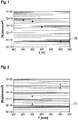
- the concentration of nitrogen [N] in the silicon epitaxial layer depends on the deposition temperature T ( Fig.1 ).
- T deposition temperature
- the nitrogen concentration in the silicon epitaxial layer is considerably lower than 1 x 10 16 atoms/cm 3 and near the detection limit (DL) of dynamic SIMS profiling. Therefore, the concentration of nitrogen in the silicon epitaxial layer can be controlled by the deposition temperature. Lowering the deposition temperature increases the nitrogen concentration.
- the concentration of nitrogen [N] in the silicon epitaxial layer can be controlled by controlling the flow rate F of the gas containing the nitrogen precursor compound ( Fig.2 ).
- the flow rate F of the gas containing the nitrogen precursor compound Fig.2
- increasing the flow rate by about 50% increases the nitrogen concentration in the silicon epitaxial layer by at least more than one order of magnitude.
- the incorporation behavior of nitrogen cannot be explained by a simple growth model. Some autocatalytic mechanism has to be taken into account.
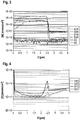
- the curve of the nitrogen concentration within the silicon epitaxial layer is almost flat (curves A1N and A2N), provided that the epitaxial wafer was not subjected to a post-epi anneal.
- Curves A1N and A2N represent the in-depth concentration of nitrogen in the silicon epitaxial layer and a part of the silicon substrate, after the deposition of the silicon epitaxial layer at a deposition temperature of 880 °C and 900 °C, respectively, and using ammonia as nitrogen precursor. In the vicinity of the interface, the nitrogen concentration switches within a pronounced transition region having a narrow width.
- Curves B1N and B2N represent the in-depth concentration of nitrogen in the silicon epitaxial layer and a part of the silicon substrate, after the deposition of the silicon epitaxial layer at a deposition temperature of 880 °C and 900 °C, respectively, and using ammonia as nitrogen precursor, and after a post-epi anneal.
- curves A2 and B2 represent the in-depth concentration of nitrogen in the silicon epitaxial layer and a part of the silicon substrate, after the deposition of the silicon epitaxial layer at a deposition temperature of 900 °C, using a deposition gas which does not include a nitrogen precursor compound, and before (A2) and after (B2) having subjected the epitaxial wafer to a post-epi anneal.
- the silicon epitaxial layer which is doped with nitrogen according to the present invention constitutes an environment for oxygen-nitrogen interaction, which allows the formation of an oxygen-enriched region having an oxygen peak-concentration in a certain depth from the surface of the epitaxial layer.
- Curves A1O and A2O represent the in-depth concentration of oxygen in the silicon epitaxial layer and a part of the silicon substrate, after the deposition of the silicon epitaxial layer at a deposition temperature of 880 °C and 900 °C, respectively, and using ammonia as nitrogen precursor.
- the oxygen-enriched region can be detected in the silicon epitaxial layer in the vicinity of the interface between the silicon epitaxial layer and the silicon substrate wafer.
- the oxygen-enriched region can already be detected directly after the deposition of the epitaxial layer, provided the concentration of nitrogen is not less than 1 x 10 19 atoms/cm 3 .
- the epitaxial wafer is subjected to a post-epi anneal.
- Curves B1O and B2O represent the in-depth concentration of oxygen in the silicon epitaxial layer and a part of the silicon substrate, after the deposition of the silicon epitaxial layer at a deposition temperature of 880 °C and 900 °C, respectively, and using ammonia as nitrogen precursor, and after a post-epi anneal.
- the silicon epitaxial layer which is doped with nitrogen acts as a sink for oxygen.
- the silicon substrate wafer constitutes a source of oxygen diffusing into the silicon epitaxial layer and interacting with nitrogen. The diffusion of oxygen starts during the deposition of the silicon epitaxial layer and is further enhanced by a subsequent post-epi anneal.
- the thermal budget of the post-epi anneal preferably corresponds to a thermal budget which is typically used for advanced CMOS processes. Therefore, the post-epi anneal may be performed by the manufacturer of the epitaxial wafer or by the manufacturer of the electronic devices.
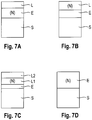
- Figs.7A to 7D display examples of epitaxial wafers.
- the epitaxial wafer according to Fig.7A representing an aspect of the present invention comprises a silicon substrate wafer S, a silicon epitaxial layer E deposited on a first side of the silicon substrate wafer and an additional epitaxial layer L deposited on top of the silicon epitaxial layer.
- the silicon epitaxial layer E is doped with nitrogen (N) in accordance with the invention, whereas the additional epitaxial layer L is not doped with nitrogen.
- the epitaxial wafer according to Fig.7B not representing the present invention comprises a silicon substrate wafer S, a silicon epitaxial layer E deposited on a first side of the silicon substrate wafer and an additional epitaxial layer L deposited on top of the silicon epitaxial layer.
- the additional epitaxial layer L is doped with nitrogen (N)
- the silicon epitaxial layer E is not doped with nitrogen.
- the epitaxial wafer according to Fig.7C not representing the present invention comprises a silicon substrate wafer S, a silicon epitaxial layer E deposited on a first side of the substrate wafer and a first additional epitaxial layer L1 deposited on top of the silicon epitaxial layer E and a second additional epitaxial layer L2 deposited on top of the first additional epitaxial layer L1.
- the first additional epitaxial layer L1 is doped with nitrogen (N), whereas the silicon epitaxial layer E and the second additional epitaxial layer L2 are not doped with nitrogen.
- the epitaxial wafer according to Fig.7D representing an aspect of the present invention comprises a silicon substrate wafer S and a silicon epitaxial layer E deposited on a first side of the silicon substrate wafer.
- the silicon epitaxial layer E is doped with nitrogen (N) in accordance with the invention.
- the strength of the silicon epitaxial layer i.e. its ability to pin dislocations, can be investigated by applying a Vickers micro-indentation test comprising three preparation steps as described in M.Akatsuka and K. Sueoka, Jpn.J.Apply.Phys, 40, (2001) 1240 .
- Step 1 a Vickers mirco-indenter is used for imprinting an indent on the silicon epitaxial layer with a defined load.
- the indent creates a mechanically stressed zone in the silicon epitaxial layer.
- Step 2 the epitaxial wafer is annealed in an Ar atmosphere for 3 hours at 1000°C in order to promote stress release in the stressed zone by nucleation and propagation of dislocations.
- Step 3 the epitaxial wafer is subjected to a Wright etch for 2 minutes in order to delineate dislocations which have nucleated and propagated during the annealing step.
- the indent and the dislocations form a rosette as shown in Fig.5
- the ability of the silicon epitaxial layer to keep metallic impurities away from regions for electronic device structures can be assessed by means of a getter test.
- the back side of the epitaxial wafer is contaminated with a defined amount of a metallic impurity, followed by a thermal treatment driving-in the impurity into the epitaxial wafer.
- the front side of the epitaxial wafer is analyzed in order to determine the fraction of impurity which was not gettered in the silicon epitaxial layer of the epitaxial wafer.
- a silicon substrate wafer is chosen which has high resistivity and low oxygen content. Such a silicon substrate wafer exhibits low intrinsic gettering capability.
- sample 1 and 2 Three different samples of epitaxial wafers were prepared, two of them representing the present invention (sample 1 and 2) and the remaining one representing a comparative example (sample 3) .
- the samples representing the invention were prepared by depositing a silicon epitaxial layer on the polished front side of a silicon substrate wafer by chemical vapor deposition in the presence of a deposition gas atmosphere containing dichlorosilane as silicon precursor compound and ammonia as nitrogen precursor compound.
- the deposition temperature was set to 880 °C.
- Samples 1 and 2 differed from each other by the concentration of nitrogen in the silicon epitaxial layer.
- Sample 3 representing the comparative example was prepared in the same manner, except that the deposition gas did not contain a nitrogen precursor compound, i.e. the silicon epitaxial layer was not doped with nitrogen.
- test supports that wafers representing the invention comprise epitaxial layers having an improved ability to impede the propagation of stress induced dislocations.
- sample 4 representing the present invention
- sample 5 representing a comparative example.
- the epitaxial wafers according to sample 4 were prepared by depositing a silicon epitaxial layer on the polished front side of a silicon substrate wafer by chemical vapor deposition in the presence of a deposition gas atmosphere containing dichlorosilane as silicon precursor compound and ammonia as nitrogen precursor compound.
- the deposition temperature was set to 880 °C.
- the silicon substrate wafer had a resistivity of 60 ⁇ cm and an oxygen concentration of 5 x 10 17 atoms/cm 3 (new ASTM) .
- the epitaxial wafers according to sample 5 were prepared in the same manner, except that the deposition gas did not contain a nitrogen precursor compound, i.e. the silicon epitaxial layer was not doped with nitrogen.
- each sample wafer was contaminated with a Ni-containing salt by spin coating.
- the Ni contamination levels chosen were 1 x 10 10 atoms/cm 2 , 1 x 10 11 atoms/cm 2 and 1 x 10 12 atoms/cm 2 .
- the sample wafers were subjected to a drive-in heat-treatment at 900 °C.
- the concentration of Ni retrieved at the surface of the silicon epitaxial layer was measured by VPD-ICP-MS.
- Table 2 summarizes the results of the getter test.
Description
- The claimed invention is directed to an epitaxial wafer and to a method for producing an epitaxial wafer.
- The epitaxial wafer comprises a silicon substrate wafer having a first side and a second side, and a silicon epitaxial layer deposited on the first side of the silicon substrate wafer.
- The method comprises depositing the silicon epitaxial layer on the first side of the silicon substrate wafer by chemical vapor deposition (CVD).
- Epitaxial wafers are used for manufacturing semiconductor devices, such as memory devices and microprocessors. Miniaturization of electronic device structures like transistors is in progress and amplifies several problems. It becomes more likely that dislocations caused by stress fields will damage or even destroy electronic device structures. Accordingly, attempts were made to strengthen the epitaxial layer against dislocation nucleation and propagation.
-
US 2010/0151692 A1 proposes to subject the epitaxial wafer to a heat treatment under a non-oxidizing atmosphere such that the oxygen concentration of the surface of the silicon epitaxial layer is set to 1.0 x 10¹⁷ to 12 x 1017 atoms/cm3. It is believed that raising the oxygen concentration in the epitaxial layer improves the resistance to dislocation generation. - Another problem concerns metallic impurities which have a detrimental effect on the functional integrity of electronic devices. Attempts were made to keep such impurities away from electronic device structures by providing gettering sites which are sinks for metallic impurities. Recent developments require shifting such gettering sites closer to the electronic device structures in order to reduce the diffusion length which impurities have to cover in order to reach the gettering sites.
-
US 2006/0175613 A1 discloses a method comprising growing a gettering layer over a semiconductor substrate and forming an epitaxial layer over the gettering layer. - According to
EP 0 265 988 A1 -
JP 2007 073820 A -
US 6 274 442 B1 is directed to a transistor comprising a barrier layer arranged upon a semiconductor substrate, wherein the barrier layer comprises a nitrogen silicon epitaxial layer. -
US 6 548 886 B1 discloses a silicon semiconductor substrate which is obtained from a silicon single crystal as grown by the CZ method and has a nitrogen content which is not less than 1 x 10¹³ atoms/cm3 and not more than 1 x 10¹⁶ atoms/cm3. - The object of the present invention is to provide a solution to the above mentioned problems which is less complex and more effective than known solutions.
- The inventors have found that the presence of nitrogen in the silicon epitaxial layer at a concentration of 4 x 10¹⁸ atoms/cm3 or more and 2 x 10¹⁹ atoms/cm3 or less reduces the nucleation and propagation of dislocations. Moreover, nitrogen incorporated into the silicon epitaxial layer in accordance with the present invention is readily accessible for oxygen-nitrogen interaction, which allows the formation of an oxygen-enriched region having an oxygen peak-concentration in a certain depth from the surface of the epitaxial layer. The oxygen-enriched region exhibits gettering activity for metallic impurities.
- According to a first aspect, the claimed invention is directed to an epitaxial wafer according to
claim 1. - An additional epitaxial layer is a further silicon epitaxial layer. According to a further aspect, the invention is directed to an epitaxial wafer according to the first aspect, wherein the silicon epitaxial layer is doped with nitrogen and an additional silicon epitaxial layer deposited on top of the silicon epitaxial layer is not doped with nitrogen.
- According to a further aspect, the invention is directed to an epitaxial wafer according to the first aspect, wherein the silicon epitaxial layer is deposited on the silicon substrate wafer to completely or partially cover the silicon substrate wafer. The presence of the silicon epitaxial layer on the substrate wafer can be restricted to regions where electronic device structures are built.
- According to a further aspect, the invention is directed to an epitaxial wafer according to the first or to a further aspect, wherein the silicon epitaxial layer is additionally doped with at least one electrically active dopant belonging to group III or group V of the periodic table of elements. Preferred dopants are boron, phosphorous, arsenic and antimony.
- According to further aspect, the invention is directed to an epitaxial wafer according to the first aspect or to a further aspect, wherein the silicon epitaxial layer doped with nitrogen comprises an oxygen-enriched region which exhibits gettering activity for metallic impurities. The concentration of oxygen in the oxygen-enriched region has an in-depth profile comprising a peak. The peak-concentration of oxygen is located in a depth direction of the silicon epitaxial layer doped with nitrogen.
- The peak-concentration of oxygen in the oxygen-enriched region is preferably 1 x 10¹⁷ atoms/cm3 or more and 1 x 10¹⁹ atoms/cm3 or less (new ASTM).
- The distance of the peak-concentration of oxygen in the oxygen-enriched region from the interface between the silicon substrate wafer and the silicon epitaxial layer is preferably 50 nm or more and 2 µm or less. The location of the peak-concentration of the oxygen-enriched region in depth direction from the surface of the silicon epitaxial layer is preferably deeper than the depth of a region intended to be used as electronically active region.
- The distance of the peak-concentration of oxygen in the oxygen-enriched region from an interface between the at least one of the one or more additional epitaxial layers which is doped with nitrogen and a lower layer adjacent thereto is preferably 50 nm or more and 2 µm or less.
- The inventors found that the diffusion coefficient of nitrogen in the silicon epitaxial layer is significantly lower than the diffusion coefficient published in literature (P.Pichler, Intrinsic Point Defects, Impurities, and Their Diffusion in Silicon, Springer (2004), p.383). The reduction of the diffusion coefficient by a factor of about 5000 suggests that nitrogen is bound in the lattice of the silicon epitaxial layer in a different manner compared to the system examined in published literature.
- According to a further aspect, the invention is directed to a method for producing an epitaxial wafer, comprising providing a silicon substrate wafer having a first side and a second side; and
depositing at a deposition temperature a silicon epitaxial layer on the first side of the silicon substrate wafer by chemical vapor deposition in the presence of a deposition gas atmosphere containing one or more silicon precursor compounds and ammonia, wherein the deposition temperature is 940°C or less and equal to or higher than a temperature which is sufficient to cause the decomposition of the one or more silicon precursor compounds and ammonia in the
deposition gas atmosphere, and wherein the silicon epitaxial layer is doped with nitrogen at a concentration of 4 x 10¹⁸ atoms/cm3 or more and 2 x 10¹⁹ atoms/cm3 or less during the deposition of the silicon epitaxial layer. - A suitable silicon substrate wafer can be obtained, e.g. by cutting a wafer from a silicon single crystal produced by the CZ method or the FZ method, and by subjecting the edge and the sides of the cut wafer to crystal damage removal and shaping operations, e.g. lapping and/or grinding, etching and polishing.
- The silicon substrate wafer has a first side (front side) and a second side (back side). It is preferred that at least the first side of the silicon substrate wafer has a polished surface. A silicon epitaxial layer is deposited on the first side of the silicon substrate wafer by chemical vapor deposition (CVD). During deposition, gases containing one or more silicon precursor compounds and ammonia flow over the silicon substrate wafer which is heated to a deposition temperature. The precursor compounds are thermally decomposed providing silicon and nitrogen for the growth of the silicon epitaxial layer.
- For example, silicon compounds such as silane (SiH4), disilane (Si2H6), dichlorosilane (SiH2Cl2) or trichlorosilane (SiHCl3) can be used as silicon precursor compounds.
- Ammonia (NH3) is used as silicon precursor compound.
- The deposition temperature is set to be equal to or higher than a temperature which is sufficient to cause the decomposition of the one or more silicon precursor compounds and the nitrogen precursor compound in the deposition gas. Moreover, the deposition temperature is set to 940°C or less, preferably 930°C or less.
- The inventors found that a deposition temperature of more than about 940°C causes the concentration of nitrogen in the silicon epitaxial layer to drop to values which are lower than 1 x 10¹⁶ atoms/cm3. These values are too low so as to significantly improve the capability of the silicon epitaxial layer to resist to nucleation and propagation of dislocations. An increase in deposition temperature can be compensated by increasing the flow of the nitrogen precursor compound.
- Epitaxial defects related to the doping with nitrogen in accordance with the invention could not be detected through defect etching, laser scattering inspection or Cross-Sectional Transmission Electron Microscopy (XTEM).
-
-
Fig.1 is a diagram displaying the concentration of nitrogen in the silicon epitaxial layer over the deposition temperature. -
Fig.2 displays the relationship between the concentration of nitrogen in the silicon layer and the flow rate of a gas containing the nitrogen precursor compound. -
Fig.3 shows the concentration of nitrogen in the silicon epitaxial layer in a depth direction from the surface of the silicon epitaxial layer towards the interface between the epitaxial silicon layer and the silicon substrate wafer. -
Fig.4 shows the concentration of oxygen in the silicon epitaxial layer in a depth direction from the surface of the silicon epitaxial layer towards the interface between the epitaxial silicon layer and the silicon substrate wafer. -
Fig.5 is a schematic top view of a rosette which is formed after a Vickers micro-indentation test. -
Fig.6 displays the in-depth profile of the concentration of nickel in tested epitaxial wafers. -
Figs. 7A to 7D display examples of epitaxial wafers. - Hereinafter, the invention is explained in more detail by referring to the drawings.
- The concentration of nitrogen [N] in the silicon epitaxial layer depends on the deposition temperature T (
Fig.1 ). In case that the deposition temperature is 960 °C and ammonia is used as nitrogen precursor compound and dichlorosilane as silicon precursor compound, then the nitrogen concentration in the silicon epitaxial layer is considerably lower than 1 x 10¹⁶ atoms/cm3 and near the detection limit (DL) of dynamic SIMS profiling. Therefore, the concentration of nitrogen in the silicon epitaxial layer can be controlled by the deposition temperature. Lowering the deposition temperature increases the nitrogen concentration. - Similarly, the concentration of nitrogen [N] in the silicon epitaxial layer can be controlled by controlling the flow rate F of the gas containing the nitrogen precursor compound
(Fig.2 ). In case that ammonia is used as nitrogen precursor compound, increasing the flow rate by about 50% (from 300 sccm to 450 seem) increases the nitrogen concentration in the silicon epitaxial layer by at least more than one order of magnitude. The incorporation behavior of nitrogen cannot be explained by a simple growth model. Some autocatalytic mechanism has to be taken into account. -
Fig.3 displays the concentration of nitrogen [N] over the depth D in a direction from the surface (D = 0 µm) of the silicon epitaxial layer towards the interface (D = 2.8 µm) between the silicon epitaxial layer and the silicon substrate wafer. The curve of the nitrogen concentration within the silicon epitaxial layer is almost flat (curves A1N and A2N), provided that the epitaxial wafer was not subjected to a post-epi anneal. Curves A1N and A2N represent the in-depth concentration of nitrogen in the silicon epitaxial layer and a part of the silicon substrate, after the deposition of the silicon epitaxial layer at a deposition temperature of 880 °C and 900 °C, respectively, and using ammonia as nitrogen precursor. In the vicinity of the interface, the nitrogen concentration switches within a pronounced transition region having a narrow width. - When the epitaxial wafer is additionally subjected to a post-epi anneal, nitrogen is partly out-diffused at the surface of the silicon epitaxial layer. Nitrogen does not diffuse into the substrate at the same rate and the concentration of nitrogen in the transition region as measured by SIMS does not change. Curves B1N and B2N represent the in-depth concentration of nitrogen in the silicon epitaxial layer and a part of the silicon substrate, after the deposition of the silicon epitaxial layer at a deposition temperature of 880 °C and 900 °C, respectively, and using ammonia as nitrogen precursor, and after a post-epi anneal. For comparison, curves A2 and B2 represent the in-depth concentration of nitrogen in the silicon epitaxial layer and a part of the silicon substrate, after the deposition of the silicon epitaxial layer at a deposition temperature of 900 °C, using a deposition gas which does not include a nitrogen precursor compound, and before (A2) and after (B2) having subjected the epitaxial wafer to a post-epi anneal.
- The silicon epitaxial layer which is doped with nitrogen according to the present invention constitutes an environment for oxygen-nitrogen interaction, which allows the formation of an oxygen-enriched region having an oxygen peak-concentration in a certain depth from the surface of the epitaxial layer.
-
Fig.4 displays the concentration of oxygen [O] over the depth D in a direction from the surface (D = 0 µm) of the silicon epitaxial layer towards the interface (D = 2.8 µm) between the silicon epitaxial layer and the silicon substrate wafer. Curves A1O and A2O represent the in-depth concentration of oxygen in the silicon epitaxial layer and a part of the silicon substrate, after the deposition of the silicon epitaxial layer at a deposition temperature of 880 °C and 900 °C, respectively, and using ammonia as nitrogen precursor. - The oxygen-enriched region can be detected in the silicon epitaxial layer in the vicinity of the interface between the silicon epitaxial layer and the silicon substrate wafer. The oxygen-enriched region can already be detected directly after the deposition of the epitaxial layer, provided the concentration of nitrogen is not less than 1 x 10¹⁹ atoms/cm3.
- Moreover, the inventors found that the peak-concentration of oxygen in the oxygen-enriched region and its width in depth direction of the silicon epitaxial layer can be further increased. For this purpose, the epitaxial wafer is subjected to a post-epi anneal. Curves B1O and B2O represent the in-depth concentration of oxygen in the silicon epitaxial layer and a part of the silicon substrate, after the deposition of the silicon epitaxial layer at a deposition temperature of 880 °C and 900 °C, respectively, and using ammonia as nitrogen precursor, and after a post-epi anneal. The silicon epitaxial layer which is doped with nitrogen acts as a sink for oxygen. The silicon substrate wafer constitutes a source of oxygen diffusing into the silicon epitaxial layer and interacting with nitrogen. The diffusion of oxygen starts during the deposition of the silicon epitaxial layer and is further enhanced by a subsequent post-epi anneal.
- The thermal budget of the post-epi anneal preferably corresponds to a thermal budget which is typically used for advanced CMOS processes. Therefore, the post-epi anneal may be performed by the manufacturer of the epitaxial wafer or by the manufacturer of the electronic devices.
-
Figs.7A to 7D display examples of epitaxial wafers.
The epitaxial wafer according toFig.7A representing an aspect of the present invention comprises a silicon substrate wafer S, a silicon epitaxial layer E deposited on a first side of the silicon substrate wafer and an additional epitaxial layer L deposited on top of the silicon epitaxial layer. The silicon epitaxial layer E is doped with nitrogen (N) in accordance with the invention, whereas the additional epitaxial layer L is not doped with nitrogen. - The epitaxial wafer according to
Fig.7B not representing the present invention comprises a silicon substrate wafer S, a silicon epitaxial layer E deposited on a first side of the silicon substrate wafer and an additional epitaxial layer L deposited on top of the silicon epitaxial layer. The additional epitaxial layer L is doped with nitrogen (N) , whereas the silicon epitaxial layer E is not doped with nitrogen. - The epitaxial wafer according to
Fig.7C not representing the present invention comprises a silicon substrate wafer S, a silicon epitaxial layer E deposited on a first side of the substrate wafer and a first additional epitaxial layer L1 deposited on top of the silicon epitaxial layer E and a second additional epitaxial layer L2 deposited on top of the first additional epitaxial layer L1. The first additional epitaxial layer L1 is doped with nitrogen (N), whereas the silicon epitaxial layer E and the second additional epitaxial layer L2 are not doped with nitrogen. - The epitaxial wafer according to
Fig.7D representing an aspect of the present invention comprises a silicon substrate wafer S and a silicon epitaxial layer E deposited on a first side of the silicon substrate wafer. The silicon epitaxial layer E is doped with nitrogen (N) in accordance with the invention. - The strength of the silicon epitaxial layer, i.e. its ability to pin dislocations, can be investigated by applying a Vickers micro-indentation test comprising three preparation steps as described in M.Akatsuka and K. Sueoka, Jpn.J.Apply.Phys, 40, (2001) 1240.
- Step 1: a Vickers mirco-indenter is used for imprinting an indent on the silicon epitaxial layer with a defined load. The indent creates a mechanically stressed zone in the silicon epitaxial layer.
- Step 2: the epitaxial wafer is annealed in an Ar atmosphere for 3 hours at 1000°C in order to promote stress release in the stressed zone by nucleation and propagation of dislocations. Step 3: the epitaxial wafer is subjected to a Wright etch for 2 minutes in order to delineate dislocations which have nucleated and propagated during the annealing step.
- After the preparation steps, the indent and the dislocations form a rosette as shown in
Fig.5 , and the size R of the rosette is calculated by the formula R = (A+B)/2, wherein A and B designate the distances which dislocations propagate from the center c of the indent towards opposed edges of the indent. Values of the size R which are relatively small indicate an effective inhibition of the propagation of dislocations. - The ability of the silicon epitaxial layer to keep metallic impurities away from regions for electronic device structures can be assessed by means of a getter test. The back side of the epitaxial wafer is contaminated with a defined amount of a metallic impurity, followed by a thermal treatment driving-in the impurity into the epitaxial wafer. Then, the front side of the epitaxial wafer is analyzed in order to determine the fraction of impurity which was not gettered in the silicon epitaxial layer of the epitaxial wafer. In order to exclude that significant gettering activity occurs in the silicon substrate wafer, a silicon substrate wafer is chosen which has high resistivity and low oxygen content. Such a silicon substrate wafer exhibits low intrinsic gettering capability.
- Three different samples of epitaxial wafers were prepared, two of them representing the present invention (
sample 1 and 2) and the remaining one representing a comparative example (sample 3) . - The samples representing the invention were prepared by depositing a silicon epitaxial layer on the polished front side of a silicon substrate wafer by chemical vapor deposition in the presence of a deposition gas atmosphere containing dichlorosilane as silicon precursor compound and ammonia as nitrogen precursor compound. The deposition temperature was set to 880 °
C. Samples -
Sample 3 representing the comparative example was prepared in the same manner, except that the deposition gas did not contain a nitrogen precursor compound, i.e. the silicon epitaxial layer was not doped with nitrogen. - The prepared samples were subjected to the Vickers micro-indentation test described above. The indents were impressed with a load of 600 mN. The following table 1 summarizes the results of the indentation test.
Table 1 Sample [N] (atoms/cm3) R (µm) 1 2 x 10¹⁹ 63 2 4 x 10¹⁸ 89 3 not doped with nitrogen 127 - The test supports that wafers representing the invention comprise epitaxial layers having an improved ability to impede the propagation of stress induced dislocations.
- Two different samples of epitaxial wafers were prepared,
sample 4 representing the present invention and sample 5 representing a comparative example. - The epitaxial wafers according to
sample 4 were prepared by depositing a silicon epitaxial layer on the polished front side of a silicon substrate wafer by chemical vapor deposition in the presence of a deposition gas atmosphere containing dichlorosilane as silicon precursor compound and ammonia as nitrogen precursor compound. The deposition temperature was set to 880 °C. The silicon substrate wafer had a resistivity of 60 Ωcm and an oxygen concentration of 5 x 10¹⁷ atoms/cm3 (new ASTM) .
The epitaxial wafers according to sample 5 were prepared in the same manner, except that the deposition gas did not contain a nitrogen precursor compound, i.e. the silicon epitaxial layer was not doped with nitrogen. - The back side of each sample wafer was contaminated with a Ni-containing salt by spin coating. The Ni contamination levels chosen were 1 x 10¹⁰ atoms/cm2, 1 x 10¹¹ atoms/cm2 and 1 x 10¹² atoms/cm2. Then, the sample wafers were subjected to a drive-in heat-treatment at 900 °C. Afterwards, the concentration of Ni retrieved at the surface of the silicon epitaxial layer was measured by VPD-ICP-MS. The following table 2 summarizes the results of the getter test.
Table 2 sample [Ni] level of contamination [Ni] level of recovery 4 1 x 10¹⁰ atoms/cm2 1.2 x 10⁹ atoms/ cm 24 1 x 10¹¹ atoms/cm2 1.3 x 10⁹ atoms/ cm 24 1 x 10¹² atoms/cm2 4 x 10¹⁰ atoms/cm2 5 1 x 10¹⁰ atoms/cm2 5.8 x 10⁹ atoms/cm2 5 1 x 10¹¹ atoms/cm2 1.9 x 10¹⁰ atoms/cm2 5 1 x 10¹² atoms/cm2 2.0 x 10¹¹ atoms/cm2 - The results support the presence of a considerable getter activity in the silicon epitaxial layer of the epitaxial wafers pertaining to the invention.
- This result was also confirmed by analyzing the in-depth concentration of Ni in the silicon epitaxial layer and a part of the silicon substrate after the drive-in heat-treatment. A UTP (ultra-trace-profiling) method comprising step-by-step etching was used for profiling the Ni concentration at distances of 50 nm, 1 µm, 2µm and 3µm from the surface of the silicon epitaxial layer of the sample wafers.
Fig.6 displays the in-depth profile found in samples 4 (S4) and 5 (S5). Epitaxial wafers pertaining to the invention were capable to considerably retain Ni from diffusing to the region close to the surface of the silicon epitaxial layer. Ni is gettered in a zone that matches the oxygen-enriched region. - The capability for gettering Ni could be enhanced by subjecting epitaxial
wafers representing sample 4 to a post-epi anneal (sample 6). The annealed epitaxial wafers were tested in an analogous manner. Table 3 summarizes the results of the getter test.Table 3 sample [Ni] level of contamination [Ni] level of recovery 6 not contaminated 1.8 x 10⁸ atoms/cm2 6 1 x 10¹⁰ atoms/cm2 8.2 x 10⁸ atoms/cm2 6 1 x 10¹¹ atoms/cm2 6.3 x 10⁹ atoms/cm2 6 1 x 10¹² atoms/cm2 3.1 x 10¹⁰ atoms/cm2
Claims (8)
- Epitaxial wafer, comprising a silicon substrate wafer having a first side and a second side, and a silicon epitaxial layer on the first side of the silicon substrate wafer, characterised in that the silicon epitaxial layer is doped with nitrogen at a concentration of 4 x 10¹⁸ atoms/cm3 or more and 2 x 10¹⁹ atoms/cm3 or less.
- Epitaxial wafer according to claim 1, wherein the silicon epitaxial layer is doped with nitrogen and an additional silicon epitaxial layer deposited on top of the silicon epitaxial layer is not doped with nitrogen.
- Epitaxial wafer according to claim 1 or claim 2, wherein the silicon epitaxial layer completely or partially covers the silicon substrate wafer.
- Epitaxial wafer according to one of claims 1 to 3, wherein the silicon epitaxial layer is additionally doped with at least one electrically active dopant belonging to group III or group V of the periodic table of elements.
- Epitaxial wafer according to one of claims 1 to 4, wherein the silicon epitaxial layer doped with nitrogen comprises an oxygen-enriched region exhibiting gettering activities and having a peak concentration of oxygen.
- A method for producing an epitaxial wafer, comprising providing a silicon substrate wafer having a first side and a second side; and
depositing at a deposition temperature a silicon epitaxial layer on the first side of the silicon substrate wafer by chemical vapor deposition in the presence of a deposition gas atmosphere containing one or more silicon precursor compounds and ammonia, wherein the deposition temperature is 940°C or less and equal to or higher than a temperature which is sufficient to cause the decomposition of the one or more silicon precursor compounds and ammonia in the deposition gas atmosphere, and wherein the silicon epitaxial layer is doped with nitrogen at a concentration of 4 x 10¹⁸ atoms/cm3 or more and 2 x 10¹⁹ atoms/cm3 or less during the deposition of the silicon epitaxial layer. - The method according to claim 6, wherein the silicon epitaxial layer is deposited in the presence of ammonia and an additional epitaxial layer is deposited on top of the silicon epitaxial layer in the absence of one or more nitrogen precursor compounds.
- Method as claimed in claims 6 or claim 7, further comprising subjecting the epitaxial wafer to a post-epi anneal.
Applications Claiming Priority (2)
| Application Number | Priority Date | Filing Date | Title |
|---|---|---|---|
| US201261733977P | 2012-12-06 | 2012-12-06 | |
| PCT/EP2013/075313 WO2014086742A1 (en) | 2012-12-06 | 2013-12-03 | Epitaxial wafer and a method of manufacturing thereof |
Publications (2)
| Publication Number | Publication Date |
|---|---|
| EP2959500A1 EP2959500A1 (en) | 2015-12-30 |
| EP2959500B1 true EP2959500B1 (en) | 2019-02-27 |
Family
ID=49681050
Family Applications (1)
| Application Number | Title | Priority Date | Filing Date |
|---|---|---|---|
| EP13798687.3A Active EP2959500B1 (en) | 2012-12-06 | 2013-12-03 | Epitaxial wafer and a method of manufacturing thereof |
Country Status (8)
| Country | Link |
|---|---|
| US (1) | US9691632B2 (en) |
| EP (1) | EP2959500B1 (en) |
| JP (1) | JP6341928B2 (en) |
| KR (1) | KR101709026B1 (en) |
| CN (1) | CN104838474B (en) |
| SG (1) | SG11201504374YA (en) |
| TW (1) | TWI541864B (en) |
| WO (1) | WO2014086742A1 (en) |
Cited By (1)
| Publication number | Priority date | Publication date | Assignee | Title |
|---|---|---|---|---|
| EP4044216A1 (en) | 2021-02-16 | 2022-08-17 | Siltronic AG | Method for testing the stress robustness of a semiconductor substrate |
Families Citing this family (5)
| Publication number | Priority date | Publication date | Assignee | Title |
|---|---|---|---|---|
| JP6032186B2 (en) * | 2013-11-29 | 2016-11-24 | 信越半導体株式会社 | Evaluation method of silicon epitaxial wafer |
| KR102610448B1 (en) * | 2016-08-12 | 2023-12-07 | 인프리아 코포레이션 | Methods of reducing metal residue in edge bead region from metal-containing resists |
| JP6299835B1 (en) * | 2016-10-07 | 2018-03-28 | 株式会社Sumco | Epitaxial silicon wafer and method of manufacturing epitaxial silicon wafer |
| JP6855124B2 (en) * | 2017-05-08 | 2021-04-07 | 株式会社ディスコ | Gettering layer formation method |
| US10943813B2 (en) * | 2018-07-13 | 2021-03-09 | Globalwafers Co., Ltd. | Radio frequency silicon on insulator wafer platform with superior performance, stability, and manufacturability |
Citations (1)
| Publication number | Priority date | Publication date | Assignee | Title |
|---|---|---|---|---|
| JP2007073820A (en) * | 2005-09-08 | 2007-03-22 | Sumco Corp | Epitaxial wafer and method for manufacturing the same |
Family Cites Families (13)
| Publication number | Priority date | Publication date | Assignee | Title |
|---|---|---|---|---|
| JPS60246297A (en) * | 1984-05-17 | 1985-12-05 | Shin Etsu Handotai Co Ltd | Preparation of nitrogen-doped silicon single crystal |
| JPS61125012A (en) | 1984-11-21 | 1986-06-12 | Toshiba Corp | Epitaxial wafer |
| IT1216212B (en) | 1986-10-29 | 1990-02-22 | S G S Microelettrica S P A | EPITAXIAL LAYERS WITH HOW MANY TA 'CONTROLLED OF NITROGEN GROWN ON SILICON SUBSTRATES |
| JP4084902B2 (en) * | 1998-05-01 | 2008-04-30 | シルトロニック・ジャパン株式会社 | Silicon semiconductor substrate and manufacturing method thereof |
| KR100541882B1 (en) * | 1998-05-01 | 2006-01-16 | 왁커 엔에스씨이 코포레이션 | Silicon Semiconductor Substrate and Method of Manufacturing the Same |
| US6274442B1 (en) * | 1998-07-15 | 2001-08-14 | Advanced Micro Devices, Inc. | Transistor having a nitrogen incorporated epitaxially grown gate dielectric and method of making same |
| US7468311B2 (en) | 2003-09-30 | 2008-12-23 | Tokyo Electron Limited | Deposition of silicon-containing films from hexachlorodisilane |
| KR100632463B1 (en) * | 2005-02-07 | 2006-10-11 | 삼성전자주식회사 | Epitaxial semiconductor substrate manufacturing method and image sensor manufacturing method, epitaxial semiconductor substrate and image sensor using same |
| US7391058B2 (en) * | 2005-06-27 | 2008-06-24 | General Electric Company | Semiconductor devices and methods of making same |
| JP2009200231A (en) | 2008-02-21 | 2009-09-03 | Sumco Corp | Epitaxial wafer and method of manufacturing the same |
| JP2009212354A (en) | 2008-03-05 | 2009-09-17 | Sumco Corp | Method of manufacturing silicon substrate |
| JP2010141272A (en) | 2008-12-15 | 2010-06-24 | Sumco Corp | Epitaxial wafer and its production method |
| JP2011253978A (en) | 2010-06-03 | 2011-12-15 | Sumco Corp | Epitaxial substrate and its manufacturing method |
-
2013
- 2013-11-27 TW TW102143188A patent/TWI541864B/en active
- 2013-12-03 SG SG11201504374YA patent/SG11201504374YA/en unknown
- 2013-12-03 KR KR1020157012326A patent/KR101709026B1/en active Active
- 2013-12-03 WO PCT/EP2013/075313 patent/WO2014086742A1/en not_active Ceased
- 2013-12-03 EP EP13798687.3A patent/EP2959500B1/en active Active
- 2013-12-03 US US14/649,114 patent/US9691632B2/en active Active
- 2013-12-03 CN CN201380063457.0A patent/CN104838474B/en active Active
- 2013-12-03 JP JP2015545773A patent/JP6341928B2/en active Active
Patent Citations (1)
| Publication number | Priority date | Publication date | Assignee | Title |
|---|---|---|---|---|
| JP2007073820A (en) * | 2005-09-08 | 2007-03-22 | Sumco Corp | Epitaxial wafer and method for manufacturing the same |
Cited By (3)
| Publication number | Priority date | Publication date | Assignee | Title |
|---|---|---|---|---|
| EP4044216A1 (en) | 2021-02-16 | 2022-08-17 | Siltronic AG | Method for testing the stress robustness of a semiconductor substrate |
| WO2022175115A1 (en) | 2021-02-16 | 2022-08-25 | Siltronic Ag | Method for testing the stress robustness of a semiconductor substrate |
| US12550680B2 (en) | 2021-02-16 | 2026-02-10 | Siltronic Ag | Method for testing the stress robustness of a semiconductor substrate |
Also Published As
| Publication number | Publication date |
|---|---|
| JP6341928B2 (en) | 2018-06-13 |
| KR20150066590A (en) | 2015-06-16 |
| TW201423843A (en) | 2014-06-16 |
| WO2014086742A1 (en) | 2014-06-12 |
| TWI541864B (en) | 2016-07-11 |
| US20150303071A1 (en) | 2015-10-22 |
| CN104838474A (en) | 2015-08-12 |
| KR101709026B1 (en) | 2017-02-21 |
| JP2016500475A (en) | 2016-01-12 |
| SG11201504374YA (en) | 2015-07-30 |
| US9691632B2 (en) | 2017-06-27 |
| CN104838474B (en) | 2018-04-27 |
| EP2959500A1 (en) | 2015-12-30 |
Similar Documents
| Publication | Publication Date | Title |
|---|---|---|
| US8278176B2 (en) | Selective epitaxial formation of semiconductor films | |
| EP2959500B1 (en) | Epitaxial wafer and a method of manufacturing thereof | |
| US8029620B2 (en) | Methods of forming carbon-containing silicon epitaxial layers | |
| EP2133908A1 (en) | Method for manufacturing deformation silicon substrate | |
| US20100258857A1 (en) | Method of Forming a Layer Comprising Epitaxial Silicon, and a Field Effect Transistor | |
| KR20070100401A (en) | Selective Deposition of Silicon-Containing Thin Films | |
| US20090321883A1 (en) | Silicon substrate for solid-state imaging device and method for manufacturing the same | |
| US9362114B2 (en) | Epitaxial wafer and method of manufacturing the same | |
| Ye et al. | High tensile strained in-situ phosphorus doped silicon epitaxial film for nMOS applications | |
| KR20160089461A (en) | Epitaxial wafer manufacturing method and epitaxial wafer | |
| US6599816B2 (en) | Method of manufacturing silicon epitaxial wafer | |
| Ma et al. | Dopant and thickness dependence of metal-induced lateral crystallization of amorphous silicon films | |
| KR100625822B1 (en) | Silicon wafer and process for producing it | |
| JP2025157587A (en) | Silicon wafers and epitaxial silicon wafers | |
| JP4972330B2 (en) | Manufacturing method of silicon epitaxial wafer | |
| US20070140828A1 (en) | Silicon wafer and method for production of silicon wafer | |
| JP7757917B2 (en) | Silicon wafers and epitaxial silicon wafers |
Legal Events
| Date | Code | Title | Description |
|---|---|---|---|
| PUAI | Public reference made under article 153(3) epc to a published international application that has entered the european phase |
Free format text: ORIGINAL CODE: 0009012 |
|
| 17P | Request for examination filed |
Effective date: 20150522 |
|
| AK | Designated contracting states |
Kind code of ref document: A1 Designated state(s): AL AT BE BG CH CY CZ DE DK EE ES FI FR GB GR HR HU IE IS IT LI LT LU LV MC MK MT NL NO PL PT RO RS SE SI SK SM TR |
|
| AX | Request for extension of the european patent |
Extension state: BA ME |
|
| DAX | Request for extension of the european patent (deleted) | ||
| 17Q | First examination report despatched |
Effective date: 20160504 |
|
| GRAP | Despatch of communication of intention to grant a patent |
Free format text: ORIGINAL CODE: EPIDOSNIGR1 |
|
| STAA | Information on the status of an ep patent application or granted ep patent |
Free format text: STATUS: GRANT OF PATENT IS INTENDED |
|
| GRAJ | Information related to disapproval of communication of intention to grant by the applicant or resumption of examination proceedings by the epo deleted |
Free format text: ORIGINAL CODE: EPIDOSDIGR1 |
|
| STAA | Information on the status of an ep patent application or granted ep patent |
Free format text: STATUS: EXAMINATION IS IN PROGRESS |
|
| INTG | Intention to grant announced |
Effective date: 20180727 |
|
| RIN1 | Information on inventor provided before grant (corrected) |
Inventor name: STORCK, PETER Inventor name: TOLCHINSKY, PETER Inventor name: YABLOK, IRWIN Inventor name: WERNER, NORBERT Inventor name: VORDERWESTNER, MARTIN |
|
| INTC | Intention to grant announced (deleted) | ||
| GRAP | Despatch of communication of intention to grant a patent |
Free format text: ORIGINAL CODE: EPIDOSNIGR1 |
|
| STAA | Information on the status of an ep patent application or granted ep patent |
Free format text: STATUS: GRANT OF PATENT IS INTENDED |
|
| INTG | Intention to grant announced |
Effective date: 20180928 |
|
| GRAS | Grant fee paid |
Free format text: ORIGINAL CODE: EPIDOSNIGR3 |
|
| GRAA | (expected) grant |
Free format text: ORIGINAL CODE: 0009210 |
|
| STAA | Information on the status of an ep patent application or granted ep patent |
Free format text: STATUS: THE PATENT HAS BEEN GRANTED |
|
| AK | Designated contracting states |
Kind code of ref document: B1 Designated state(s): AL AT BE BG CH CY CZ DE DK EE ES FI FR GB GR HR HU IE IS IT LI LT LU LV MC MK MT NL NO PL PT RO RS SE SI SK SM TR |
|
| REG | Reference to a national code |
Ref country code: GB Ref legal event code: FG4D |
|
| REG | Reference to a national code |
Ref country code: CH Ref legal event code: EP |
|
| REG | Reference to a national code |
Ref country code: AT Ref legal event code: REF Ref document number: 1102548 Country of ref document: AT Kind code of ref document: T Effective date: 20190315 |
|
| REG | Reference to a national code |
Ref country code: IE Ref legal event code: FG4D |
|
| REG | Reference to a national code |
Ref country code: DE Ref legal event code: R096 Ref document number: 602013051515 Country of ref document: DE |
|
| REG | Reference to a national code |
Ref country code: NL Ref legal event code: MP Effective date: 20190227 |
|
| REG | Reference to a national code |
Ref country code: LT Ref legal event code: MG4D |
|
| PG25 | Lapsed in a contracting state [announced via postgrant information from national office to epo] |
Ref country code: LT Free format text: LAPSE BECAUSE OF FAILURE TO SUBMIT A TRANSLATION OF THE DESCRIPTION OR TO PAY THE FEE WITHIN THE PRESCRIBED TIME-LIMIT Effective date: 20190227 Ref country code: NL Free format text: LAPSE BECAUSE OF FAILURE TO SUBMIT A TRANSLATION OF THE DESCRIPTION OR TO PAY THE FEE WITHIN THE PRESCRIBED TIME-LIMIT Effective date: 20190227 Ref country code: SE Free format text: LAPSE BECAUSE OF FAILURE TO SUBMIT A TRANSLATION OF THE DESCRIPTION OR TO PAY THE FEE WITHIN THE PRESCRIBED TIME-LIMIT Effective date: 20190227 Ref country code: NO Free format text: LAPSE BECAUSE OF FAILURE TO SUBMIT A TRANSLATION OF THE DESCRIPTION OR TO PAY THE FEE WITHIN THE PRESCRIBED TIME-LIMIT Effective date: 20190527 Ref country code: FI Free format text: LAPSE BECAUSE OF FAILURE TO SUBMIT A TRANSLATION OF THE DESCRIPTION OR TO PAY THE FEE WITHIN THE PRESCRIBED TIME-LIMIT Effective date: 20190227 Ref country code: PT Free format text: LAPSE BECAUSE OF FAILURE TO SUBMIT A TRANSLATION OF THE DESCRIPTION OR TO PAY THE FEE WITHIN THE PRESCRIBED TIME-LIMIT Effective date: 20190627 |
|
| PG25 | Lapsed in a contracting state [announced via postgrant information from national office to epo] |
Ref country code: IS Free format text: LAPSE BECAUSE OF FAILURE TO SUBMIT A TRANSLATION OF THE DESCRIPTION OR TO PAY THE FEE WITHIN THE PRESCRIBED TIME-LIMIT Effective date: 20190627 Ref country code: LV Free format text: LAPSE BECAUSE OF FAILURE TO SUBMIT A TRANSLATION OF THE DESCRIPTION OR TO PAY THE FEE WITHIN THE PRESCRIBED TIME-LIMIT Effective date: 20190227 Ref country code: HR Free format text: LAPSE BECAUSE OF FAILURE TO SUBMIT A TRANSLATION OF THE DESCRIPTION OR TO PAY THE FEE WITHIN THE PRESCRIBED TIME-LIMIT Effective date: 20190227 Ref country code: GR Free format text: LAPSE BECAUSE OF FAILURE TO SUBMIT A TRANSLATION OF THE DESCRIPTION OR TO PAY THE FEE WITHIN THE PRESCRIBED TIME-LIMIT Effective date: 20190528 Ref country code: RS Free format text: LAPSE BECAUSE OF FAILURE TO SUBMIT A TRANSLATION OF THE DESCRIPTION OR TO PAY THE FEE WITHIN THE PRESCRIBED TIME-LIMIT Effective date: 20190227 Ref country code: BG Free format text: LAPSE BECAUSE OF FAILURE TO SUBMIT A TRANSLATION OF THE DESCRIPTION OR TO PAY THE FEE WITHIN THE PRESCRIBED TIME-LIMIT Effective date: 20190527 |
|
| REG | Reference to a national code |
Ref country code: AT Ref legal event code: MK05 Ref document number: 1102548 Country of ref document: AT Kind code of ref document: T Effective date: 20190227 |
|
| PG25 | Lapsed in a contracting state [announced via postgrant information from national office to epo] |
Ref country code: ES Free format text: LAPSE BECAUSE OF FAILURE TO SUBMIT A TRANSLATION OF THE DESCRIPTION OR TO PAY THE FEE WITHIN THE PRESCRIBED TIME-LIMIT Effective date: 20190227 Ref country code: DK Free format text: LAPSE BECAUSE OF FAILURE TO SUBMIT A TRANSLATION OF THE DESCRIPTION OR TO PAY THE FEE WITHIN THE PRESCRIBED TIME-LIMIT Effective date: 20190227 Ref country code: CZ Free format text: LAPSE BECAUSE OF FAILURE TO SUBMIT A TRANSLATION OF THE DESCRIPTION OR TO PAY THE FEE WITHIN THE PRESCRIBED TIME-LIMIT Effective date: 20190227 Ref country code: EE Free format text: LAPSE BECAUSE OF FAILURE TO SUBMIT A TRANSLATION OF THE DESCRIPTION OR TO PAY THE FEE WITHIN THE PRESCRIBED TIME-LIMIT Effective date: 20190227 Ref country code: RO Free format text: LAPSE BECAUSE OF FAILURE TO SUBMIT A TRANSLATION OF THE DESCRIPTION OR TO PAY THE FEE WITHIN THE PRESCRIBED TIME-LIMIT Effective date: 20190227 Ref country code: IT Free format text: LAPSE BECAUSE OF FAILURE TO SUBMIT A TRANSLATION OF THE DESCRIPTION OR TO PAY THE FEE WITHIN THE PRESCRIBED TIME-LIMIT Effective date: 20190227 Ref country code: AL Free format text: LAPSE BECAUSE OF FAILURE TO SUBMIT A TRANSLATION OF THE DESCRIPTION OR TO PAY THE FEE WITHIN THE PRESCRIBED TIME-LIMIT Effective date: 20190227 Ref country code: SK Free format text: LAPSE BECAUSE OF FAILURE TO SUBMIT A TRANSLATION OF THE DESCRIPTION OR TO PAY THE FEE WITHIN THE PRESCRIBED TIME-LIMIT Effective date: 20190227 |
|
| REG | Reference to a national code |
Ref country code: DE Ref legal event code: R097 Ref document number: 602013051515 Country of ref document: DE |
|
| PG25 | Lapsed in a contracting state [announced via postgrant information from national office to epo] |
Ref country code: PL Free format text: LAPSE BECAUSE OF FAILURE TO SUBMIT A TRANSLATION OF THE DESCRIPTION OR TO PAY THE FEE WITHIN THE PRESCRIBED TIME-LIMIT Effective date: 20190227 Ref country code: SM Free format text: LAPSE BECAUSE OF FAILURE TO SUBMIT A TRANSLATION OF THE DESCRIPTION OR TO PAY THE FEE WITHIN THE PRESCRIBED TIME-LIMIT Effective date: 20190227 |
|
| PG25 | Lapsed in a contracting state [announced via postgrant information from national office to epo] |
Ref country code: AT Free format text: LAPSE BECAUSE OF FAILURE TO SUBMIT A TRANSLATION OF THE DESCRIPTION OR TO PAY THE FEE WITHIN THE PRESCRIBED TIME-LIMIT Effective date: 20190227 |
|
| PLBE | No opposition filed within time limit |
Free format text: ORIGINAL CODE: 0009261 |
|
| STAA | Information on the status of an ep patent application or granted ep patent |
Free format text: STATUS: NO OPPOSITION FILED WITHIN TIME LIMIT |
|
| 26N | No opposition filed |
Effective date: 20191128 |
|
| PG25 | Lapsed in a contracting state [announced via postgrant information from national office to epo] |
Ref country code: SI Free format text: LAPSE BECAUSE OF FAILURE TO SUBMIT A TRANSLATION OF THE DESCRIPTION OR TO PAY THE FEE WITHIN THE PRESCRIBED TIME-LIMIT Effective date: 20190227 |
|
| PG25 | Lapsed in a contracting state [announced via postgrant information from national office to epo] |
Ref country code: TR Free format text: LAPSE BECAUSE OF FAILURE TO SUBMIT A TRANSLATION OF THE DESCRIPTION OR TO PAY THE FEE WITHIN THE PRESCRIBED TIME-LIMIT Effective date: 20190227 |
|
| REG | Reference to a national code |
Ref country code: CH Ref legal event code: PL |
|
| REG | Reference to a national code |
Ref country code: BE Ref legal event code: MM Effective date: 20191231 |
|
| PG25 | Lapsed in a contracting state [announced via postgrant information from national office to epo] |
Ref country code: MC Free format text: LAPSE BECAUSE OF FAILURE TO SUBMIT A TRANSLATION OF THE DESCRIPTION OR TO PAY THE FEE WITHIN THE PRESCRIBED TIME-LIMIT Effective date: 20190227 |
|
| GBPC | Gb: european patent ceased through non-payment of renewal fee |
Effective date: 20191203 |
|
| PG25 | Lapsed in a contracting state [announced via postgrant information from national office to epo] |
Ref country code: IE Free format text: LAPSE BECAUSE OF NON-PAYMENT OF DUE FEES Effective date: 20191203 Ref country code: LU Free format text: LAPSE BECAUSE OF NON-PAYMENT OF DUE FEES Effective date: 20191203 Ref country code: GB Free format text: LAPSE BECAUSE OF NON-PAYMENT OF DUE FEES Effective date: 20191203 |
|
| PG25 | Lapsed in a contracting state [announced via postgrant information from national office to epo] |
Ref country code: BE Free format text: LAPSE BECAUSE OF NON-PAYMENT OF DUE FEES Effective date: 20191231 Ref country code: LI Free format text: LAPSE BECAUSE OF NON-PAYMENT OF DUE FEES Effective date: 20191231 Ref country code: CH Free format text: LAPSE BECAUSE OF NON-PAYMENT OF DUE FEES Effective date: 20191231 |
|
| PG25 | Lapsed in a contracting state [announced via postgrant information from national office to epo] |
Ref country code: CY Free format text: LAPSE BECAUSE OF FAILURE TO SUBMIT A TRANSLATION OF THE DESCRIPTION OR TO PAY THE FEE WITHIN THE PRESCRIBED TIME-LIMIT Effective date: 20190227 |
|
| PG25 | Lapsed in a contracting state [announced via postgrant information from national office to epo] |
Ref country code: MT Free format text: LAPSE BECAUSE OF FAILURE TO SUBMIT A TRANSLATION OF THE DESCRIPTION OR TO PAY THE FEE WITHIN THE PRESCRIBED TIME-LIMIT Effective date: 20190227 Ref country code: HU Free format text: LAPSE BECAUSE OF FAILURE TO SUBMIT A TRANSLATION OF THE DESCRIPTION OR TO PAY THE FEE WITHIN THE PRESCRIBED TIME-LIMIT; INVALID AB INITIO Effective date: 20131203 |
|
| PG25 | Lapsed in a contracting state [announced via postgrant information from national office to epo] |
Ref country code: MK Free format text: LAPSE BECAUSE OF FAILURE TO SUBMIT A TRANSLATION OF THE DESCRIPTION OR TO PAY THE FEE WITHIN THE PRESCRIBED TIME-LIMIT Effective date: 20190227 |
|
| REG | Reference to a national code |
Ref country code: DE Ref legal event code: R079 Ref document number: 602013051515 Country of ref document: DE Free format text: PREVIOUS MAIN CLASS: H01L0021200000 Ipc: H10P0014200000 |
|
| PGFP | Annual fee paid to national office [announced via postgrant information from national office to epo] |
Ref country code: DE Payment date: 20251211 Year of fee payment: 13 |
|
| PGFP | Annual fee paid to national office [announced via postgrant information from national office to epo] |
Ref country code: FR Payment date: 20251223 Year of fee payment: 13 |