EP2957856A1 - Sensor signal detector - Google Patents
Sensor signal detector Download PDFInfo
- Publication number
- EP2957856A1 EP2957856A1 EP15172160.2A EP15172160A EP2957856A1 EP 2957856 A1 EP2957856 A1 EP 2957856A1 EP 15172160 A EP15172160 A EP 15172160A EP 2957856 A1 EP2957856 A1 EP 2957856A1
- Authority
- EP
- European Patent Office
- Prior art keywords
- signal
- reference signal
- sensor signal
- sensor
- trigger
- Prior art date
- Legal status (The legal status is an assumption and is not a legal conclusion. Google has not performed a legal analysis and makes no representation as to the accuracy of the status listed.)
- Granted
Links
Images




Classifications
-
- G—PHYSICS
- G01—MEASURING; TESTING
- G01H—MEASUREMENT OF MECHANICAL VIBRATIONS OR ULTRASONIC, SONIC OR INFRASONIC WAVES
- G01H11/00—Measuring mechanical vibrations or ultrasonic, sonic or infrasonic waves by detecting changes in electric or magnetic properties
- G01H11/06—Measuring mechanical vibrations or ultrasonic, sonic or infrasonic waves by detecting changes in electric or magnetic properties by electric means
- G01H11/08—Measuring mechanical vibrations or ultrasonic, sonic or infrasonic waves by detecting changes in electric or magnetic properties by electric means using piezoelectric devices
-
- G—PHYSICS
- G01—MEASURING; TESTING
- G01B—MEASURING LENGTH, THICKNESS OR SIMILAR LINEAR DIMENSIONS; MEASURING ANGLES; MEASURING AREAS; MEASURING IRREGULARITIES OF SURFACES OR CONTOURS
- G01B7/00—Measuring arrangements characterised by the use of electric or magnetic techniques
- G01B7/004—Measuring arrangements characterised by the use of electric or magnetic techniques for measuring coordinates of points
- G01B7/008—Measuring arrangements characterised by the use of electric or magnetic techniques for measuring coordinates of points using coordinate measuring machines
- G01B7/012—Contact-making feeler heads therefor
-
- G—PHYSICS
- G06—COMPUTING OR CALCULATING; COUNTING
- G06F—ELECTRIC DIGITAL DATA PROCESSING
- G06F3/00—Input arrangements for transferring data to be processed into a form capable of being handled by the computer; Output arrangements for transferring data from processing unit to output unit, e.g. interface arrangements
- G06F3/01—Input arrangements or combined input and output arrangements for interaction between user and computer
- G06F3/03—Arrangements for converting the position or the displacement of a member into a coded form
- G06F3/033—Pointing devices displaced or positioned by the user, e.g. mice, trackballs, pens or joysticks; Accessories therefor
- G06F3/0354—Pointing devices displaced or positioned by the user, e.g. mice, trackballs, pens or joysticks; Accessories therefor with detection of two-dimensional [2D] relative movements between the device, or an operating part thereof, and a plane or surface, e.g. 2D mice, trackballs, pens or pucks
- G06F3/03545—Pens or stylus
-
- G—PHYSICS
- G06—COMPUTING OR CALCULATING; COUNTING
- G06F—ELECTRIC DIGITAL DATA PROCESSING
- G06F3/00—Input arrangements for transferring data to be processed into a form capable of being handled by the computer; Output arrangements for transferring data from processing unit to output unit, e.g. interface arrangements
- G06F3/01—Input arrangements or combined input and output arrangements for interaction between user and computer
- G06F3/03—Arrangements for converting the position or the displacement of a member into a coded form
- G06F3/041—Digitisers, e.g. for touch screens or touch pads, characterised by the transducing means
- G06F3/043—Digitisers, e.g. for touch screens or touch pads, characterised by the transducing means using propagating acoustic waves
- G06F3/0433—Digitisers, e.g. for touch screens or touch pads, characterised by the transducing means using propagating acoustic waves in which the acoustic waves are either generated by a movable member and propagated within a surface layer or propagated within a surface layer and captured by a movable member
-
- H—ELECTRICITY
- H03—ELECTRONIC CIRCUITRY
- H03K—PULSE TECHNIQUE
- H03K5/00—Manipulating of pulses not covered by one of the other main groups of this subclass
- H03K5/01—Shaping pulses
- H03K5/08—Shaping pulses by limiting; by thresholding; by slicing, i.e. combined limiting and thresholding
- H03K5/082—Shaping pulses by limiting; by thresholding; by slicing, i.e. combined limiting and thresholding with an adaptive threshold
- H03K5/086—Shaping pulses by limiting; by thresholding; by slicing, i.e. combined limiting and thresholding with an adaptive threshold generated by feedback
- H03K5/088—Shaping pulses by limiting; by thresholding; by slicing, i.e. combined limiting and thresholding with an adaptive threshold generated by feedback modified by switching, e.g. by a periodic signal or by a signal in synchronism with the transitions of the output signal
Definitions
- the present invention relates to a sensor signal detector, more specifically to a contact detector circuit of a vibration touch signal probe that detects a contact based on a change in vibration status of a stylus.
- Height gauges, coordinate measuring machines, profile measuring machines and the like have been known as measuring machines that measure shape and dimension of an object to be measured (sometimes simply referred to as an "object” hereinafter).
- contact-type measuring machines use a touch signal probe that is configured to detect a contact with an object to be measured.
- touch signal probes there are various types of known touch signal probes, one of which is an ultrasonic touch trigger probe (see, for instance, Patent Literature 1: JP-A-06-221806 ).
- the ultrasonic touch trigger probe applies vibrations to a stylus using a piezoelectric element and monitors amplitudes and/or frequency change of the vibrations to detect a contact with an object.
- the piezoelectric element In detecting a contact using the piezoelectric element, the piezoelectric element is resonantly excited by a positive feedback control and generates a detection output signal in a form of a sinusoidal signal, which is outputted from a detection electrode of the piezoelectric element.
- the amplitude and frequency of the sinusoidal signal varies when a contact piece touches an object to be measured. For instance, in order to detect a contact based on amplitude information, an amplitude change detector is used in a first typical contact detector circuit as shown in Fig. 6 .
- the amplitude change detector detects and extracts only the amplitude information from the obtained sinusoidal signal to obtain a DC sensor signal S, and generates a trigger signal TG at a point where a DC level of the DC sensor signal S is rapidly decreased due to the contact.
- the amplitude change detector generates the trigger signal TG based on a comparison between the DC sensor signal S and a constant reference electric potential VREF.
- the probe may erroneously detect a contact with an object although the probe actually does not touch the object.
- the erroneous detection occurs for the following reason.
- the DC sensor signal S has a DC offset component, a low-frequency state change component showing a slow amplitude change due to beat etc. and a high-frequency noise component that are superimposed with each other.
- the low-frequency state change component and the high-frequency noise components are overlapped with the reference electric potential VREF at a point other than the point at which the DC level of the DC sensor signal S rapidly varies as shown in Fig. 6 .
- the amplitude change detector occasionally erroneously detects that the probe touches the object and outputs a detection signal in error.
- the erroneous detection accounts for a large part of errors in the physical amount to be detected.
- the DC offset component S0 and the low-frequency state change component S1 are extracted from the DC sensor signal S using a low-pass filter, and the amplitude of the DC sensor signal (S0+S1) including the low-frequency state change component S1 is converted to obtain a reference signal (signal K(S0 + S1)) (see, for instance, Patent Literature 2: JP-A-10-111143 ).
- a second typical contact detector circuit shown in Fig. 7 sometimes detects that the probe is out of contact with the object and issues an erroneous signal even while the probe is still in contact with the object.
- Patent Literature 3 The technique disclosed in the Patent Literature 3 is based on the disclosure of the above-described Patent Literature 2.
- a third typical contact detection circuit 300 disclosed in the Patent Literature 3 includes a low-pass filter 301, a converter circuit 302, a selector circuit 303, a comparator circuit 304 and a converter circuit 305.
- the above-described third typical contact detection circuit 300 compares a DC sensor signal S and a reference signal R using the comparator circuit 304, and generates a trigger signal TG when the DC sensor signal S falls below the reference signal R.
- the value of R1 varies in accordance with (SO + S1).
- the selector circuit 303 uses the calculated signal R2 is used as the reference signal R.
- the value of the signal R2 is constant and unchanged.
- An object of the invention is to provide a sensor signal detector that is capable of appropriately detecting a sensor signal with a simple arrangement.
- a sensor signal detector is configured to detect a change in a DC sensor signal based on a change in a physical amount to be detected, the sensor signal detector including: a reference signal generator that is configured to generate a reference signal from the DC sensor signal; a trigger signal output unit that is configured to compare the DC sensor signal with the reference signal and outputs a trigger signal based on a result of a comparison between the DC sensor signal and the reference signal; and a reference signal holder that is configured to hold the reference signal when the trigger signal is started to be outputted, the held reference signal being outputted to the trigger signal output unit while the trigger signal is outputted, the trigger signal output unit using the reference signal outputted by the reference signal holder for the comparison between the DC sensor signal and the reference signal while the trigger signal is outputted.
- the reference signal is generated from the DC sensor signal, the DC sensor signal is compared with the reference signal and the trigger signal is outputted based on a result of the comparison. Further, when the trigger signal is outputted, the reference signal when the trigger signal is started to be outputted is held and the held reference signal is outputted to the trigger signal output unit while the trigger signal is outputted.
- the reference signal at the start of the output of the trigger signal is held and the held reference signal is used for the subsequent comparison with the sensor signal.
- the DC sensor signal can be stably compared with the reference signal while the trigger signal is outputted, thereby accurately detecting the sensor signal.
- the reference signal may preferably be held at the reference signal holder by storing an electric charge in a capacitor to hold a voltage.
- the reference signal is held at the reference signal holder by storing an electric charge in a capacitor to hold a voltage.
- the reference signal holder holds the reference signal not by software but by a hardware including the capacitor. Accordingly, unlike an instance in which the reference signal is calculated and held, it is not necessary to provide software for holding the reference signal, so that the structure of the sensor signal detector can be simplified.
- the DC sensor signal may preferably include a DC-level fluctuation component, a low-frequency state change component and a high-frequency noise component being superimposed with each other
- the sensor signal detector may further include a low-pass filter that is configured to receive the DC sensor signal and block the high-frequency noise component and the DC-level fluctuation component in the received DC sensor signal to output the low-frequency state change component
- the DC sensor signal passing through the low-pass filter may preferably be used for the comparison with the reference signal in the trigger signal output unit.
- the DC sensor signal passes through the low-pass filter, so that the high-frequency noise component and the rapidly varying DC-level fluctuation component (component to be detected) are removed, thereby obtaining the DC sensor signal including solely the low-frequency state change component.
- the DC sensor signal thus obtained is used for the comparison with the reference signal, so that the sensor signal can be more accurately detected.
- the DC sensor signal may preferably be obtained by extracting amplitude information from a sinusoidal output signal of a touch signal probe driven by a piezoelectric element.
- the DC sensor signal obtained by extracting the amplitude information from the sinusoidal output signal generated by the touch signal probe is a composite signal in which various components are superimposed.
- a state change component due to a temperature change, time-dependent change or the like is contained in the various components.
- the state change component is contained in both of the DC sensor signal and the reference signal. In other words, the influence of the status change is not exerted on the comparison between the DC sensor signal and the reference signal. Accordingly, the DC level changes can be reliably detected only by appropriately setting a ratio of the amplitude conversion of the noise component.
- Fig. 1 is a schematic illustration of a contact sensor using a sensor signal detector according to an exemplary embodiment of the invention as a contact detector circuit 9.
- the contact sensor includes a stylus I having a spherical contact piece 3 at an end thereof.
- the stylus I also includes a balancer 4 for keeping an attitude of the stylus 1 at a base end thereof.
- the stylus 1 is held by a stylus holder 2 approximately at a middle portion in an axial direction thereof.
- a piezoelectric element 5 that is configured to apply vibrations to the stylus 1 is attached approximately to the middle portion of the stylus 1.
- the piezoelectric element 5 includes a vibration electrode 51 configured to apply vibrations to the stylus I and a detection electrode 52 configured to detect a contact of the contact piece 3.
- a drive signal is sent to the vibration electrode 51 from a driver circuit 8.
- the detection electrode 52 generates a mechanical-electrical conversion output signal.
- the mechanical-electrical conversion output signal is detected by a detector circuit 6.
- An output signal of the detector circuit 6 is sent to the driver circuit 8 by a positive feedback.
- the feedback control excites the piezoelectric element 5 at a predetermined resonance frequency.
- the detector circuit 6 outputs a detection output signal in a form of a sinusoidal signal of which amplitude decreases when the contact piece 3 touches an object.
- An amplitude filter circuit 7 detects the sinusoidal signal obtained by the detection electrode 52 of the piezoelectric element 5 of the detector circuit 6, and extracts only amplitude information of the sinusoidal signal to output a DC sensor signal S.
- the amplitude filter circuit 7 exemplarily includes a full-wave rectifier for converting AC (Alternating Current) into DC (Direct Current), and a smoothing circuit for smoothing an AC component remaining after a rectification.
- the contact detector circuit 9 detects a variation in a DC-level fluctuation component S3 (see Figs. 2 and 4 ) in the DC sensor signal S that rapidly decreases due to a contact with the contact piece 3, and outputs a trigger signal TG.
- the contact detector circuit 9 includes: a low-pass filter 21 (low-pass filter) into which the DC sensor signal S is inputted; a reference signal generation circuit 22 (reference signal generator) that converts a level of an output signal of the low-pass filter 21; a sampling-and-holding circuit (reference signal holder) 23 that samples and/or holds an output signal of the reference signal generation circuit 22; and a trigger signal output circuit (trigger signal output unit) 24 that generates and outputs a trigger signal TG based on a result of a comparison between the DC sensor signal S and an output signal of the sampling-and-holding circuit 23.
- the low-pass filter 21 blocks the high-frequency noise component S2 and the DC-level fluctuation component S3 and passes only the DC offset component S0 and the low-frequency state change component S1 (i.e. S0 + S1) out of the components of the DC sensor signal S.
- the signal R1 is selectively used as a later-described reference signal R.
- the coefficient K is set excessively small, the trigger signal TG is generated at a timing different from an actual contact time between the contact piece 3 and the object. Accordingly, the coefficient K is preferably set as large as possible as long as the contact detection is not influenced by the high-frequency noise component S2.
- the sampling-and-holding circuit 23 holds a signal Rt1 when the trigger signal TG is started to be outputted, and keeps outputting the held signal to a comparator as the reference signal R while the trigger signal TG is kept on being outputted.
- the output signal of the sampling-and-holding circuit 23 the signal R1 (a variable value) when the trigger signal TG is not outputted, whereas the output signal becomes signal Rt I (a fixed value) when the trigger signal TG is outputted.
- the sampling-and-holding circuit 23 includes a switch 231 and a capacitor 232.
- the switch 231 is configured to be set ON when the trigger signal TG is not outputted and to be set OFF when the trigger signal TG is outputted.
- the sampling of the signal R1 by the sampling-and-holding circuit 23 is performed when the switch 231 is set ON.
- the reference signal R is held by the sampling-and-holding circuit 23 when the switch 231 is set OFF.
- the contact piece 3 of the stylus 1 is initially separated from an object (not shown) (non-contact state); the contact piece 3 then is brought into contact with the object and the contact state between the contact piece 3 and the object is kept for a while; and the contact piece 3 is again separated from the object (transitioning into the non-contact state).
- Step 1 when the DC sensor signal S is inputted to the low-pass filter 21 (Step 1 (abbreviated as "ST1" [ST2, ST3...] in the drawings), the high-frequency noise component S2 and the (transitional) DC-level fluctuation component S3 are blocked so that only the DC offset component S0 and the low-frequency state change component S1 (i.e. signal (SO + S1)) are extracted to be outputted (Step 2).
- Step 4 YES ⁇ NO.
- the trigger signal TG is outputted (Step 7), and the reference signal R is held by the sampling-and-holding circuit 23.
- the reference signal R is held at the value Rt1 during the period from the time t1 to a time t2 (Step 8).
- the DC sensor signal S rapidly increases, so that the DC sensor signal S exceeds the signal R1 at the time t2 (Step 4: NO ⁇ YES).
- the reference signal R is switched from the fixed value (signal Rt1) to the variable value (the signal R1) after the time t2.
- the signal R1 variable component derived from the DC sensor signal S
- the signal Rt1 fixed value
- the reference signal R when the trigger signal TG is outputted (i.e. in the contact state of the contact piece 3).
- the fixed value of the signal R2 is set at the value of the reference signal R when the trigger signal TG is started to be outputted.
- the value of the reference signal R is set at the value of the signal R2 by being held at the value at the sampling-and-holding circuit 23.
- the invention is also applicable to an instance where the amplitude or the like of the DC-level fluctuation component S3 increases when a contact is detected. It should be noted that, in such an instance, the value of the coefficient K has to be set greater than 1 (K > 1).
- the scope of the invention is not restricted thereto.
- the invention is applicable to an instance for detecting the frequency and/or phase of the DC sensor signal S to detect a contact based on the change in the frequency and/or phase.
- the invention is applicable to any sensor that employs a DC sensor signal S including a low-frequency state change component S1.
- sampling-and-holding circuit 23 in the above exemplary embodiment is provided by a hardware including the switch 231 and the capacitor 232, the sampling-and-holding circuit 23 may alternatively be provided by a software.
- the contact piece 3 in the above exemplary embodiment keeps in contact with the object for a while from an initial non-contact state, and subsequently returns to the non-contact state
- the invention is also applicable to an instance in which the contact piece 3 is not restored to the non-contact state from the contact state and is kept to be in the contact state for a long time.
- the reference signal R is switched from the variable signal R1 to the signal Rt1 of the fixed value (Step 8) simultaneously with the output of the trigger signal TG (the time t1) (Step 7) in the above exemplary embodiment, it is not necessary that the signals are switched at the time t1 but may alternatively be switched at a predetermined time after the time t1.
- the reference signal R is switched from the signal Rt1 of the fixed value to the variable signal R1 (S6) simultaneously with the stop of the output of the trigger signal TG (the time t2) (S5) in the above exemplary embodiment, it is not necessary that the signals are switched at the time t2 but may alternatively be switched a predetermined time after the time t2.
- the sensor signal detector in the above exemplary embodiment is provided in a form of the contact detector circuit 9, the invention may alternatively be provided in a form of a pressure detector circuit and an acceleration detector circuit.
Landscapes
- Engineering & Computer Science (AREA)
- Physics & Mathematics (AREA)
- General Physics & Mathematics (AREA)
- General Engineering & Computer Science (AREA)
- Theoretical Computer Science (AREA)
- Human Computer Interaction (AREA)
- Nonlinear Science (AREA)
- Acoustics & Sound (AREA)
- Measurement Of Length, Angles, Or The Like Using Electric Or Magnetic Means (AREA)
Abstract
Description
- The present invention relates to a sensor signal detector, more specifically to a contact detector circuit of a vibration touch signal probe that detects a contact based on a change in vibration status of a stylus.
- Height gauges, coordinate measuring machines, profile measuring machines and the like have been known as measuring machines that measure shape and dimension of an object to be measured (sometimes simply referred to as an "object" hereinafter). Among such measuring machines, contact-type measuring machines use a touch signal probe that is configured to detect a contact with an object to be measured. There are various types of known touch signal probes, one of which is an ultrasonic touch trigger probe (see, for instance, Patent Literature 1:
JP-A-06-221806 - In detecting a contact using the piezoelectric element, the piezoelectric element is resonantly excited by a positive feedback control and generates a detection output signal in a form of a sinusoidal signal, which is outputted from a detection electrode of the piezoelectric element. The amplitude and frequency of the sinusoidal signal varies when a contact piece touches an object to be measured. For instance, in order to detect a contact based on amplitude information, an amplitude change detector is used in a first typical contact detector circuit as shown in
Fig. 6 . The amplitude change detector detects and extracts only the amplitude information from the obtained sinusoidal signal to obtain a DC sensor signal S, and generates a trigger signal TG at a point where a DC level of the DC sensor signal S is rapidly decreased due to the contact. The amplitude change detector generates the trigger signal TG based on a comparison between the DC sensor signal S and a constant reference electric potential VREF. - However, when the reference electric potential VREF of a constant value is used for contact detection of a probe, the probe may erroneously detect a contact with an object although the probe actually does not touch the object. The erroneous detection occurs for the following reason. In most cases, the DC sensor signal S has a DC offset component, a low-frequency state change component showing a slow amplitude change due to beat etc. and a high-frequency noise component that are superimposed with each other. Accordingly, depending on a setting of the reference electric potential VREF, the low-frequency state change component and the high-frequency noise components are overlapped with the reference electric potential VREF at a point other than the point at which the DC level of the DC sensor signal S rapidly varies as shown in
Fig. 6 . At such a point, the amplitude change detector occasionally erroneously detects that the probe touches the object and outputs a detection signal in error. The erroneous detection accounts for a large part of errors in the physical amount to be detected. - In order to avoid such an erroneous detection, as shown in
Fig. 7 , the DC offset component S0 and the low-frequency state change component S1 are extracted from the DC sensor signal S using a low-pass filter, and the amplitude of the DC sensor signal (S0+S1) including the low-frequency state change component S1 is converted to obtain a reference signal (signal K(S0 + S1)) (see, for instance, Patent Literature 2:JP-A-10-111143 - However, as shown in
Fig. 7 , when, for instance, the touch signal probe is kept in contact with the object, a second typical contact detector circuit shown inFig. 7 sometimes detects that the probe is out of contact with the object and issues an erroneous signal even while the probe is still in contact with the object. - A technique for avoiding the above-described erroneous contact detection and erroneous non-contact detection has been proposed (see, for instance,
Patent Literature 3,JP-A-2009-276238 - The technique disclosed in the
Patent Literature 3 is based on the disclosure of the above-describedPatent Literature 2. - As shown in
Fig. 8 , a third typicalcontact detection circuit 300 disclosed in thePatent Literature 3 includes a low-pass filter 301, aconverter circuit 302, aselector circuit 303, acomparator circuit 304 and aconverter circuit 305. - As shown in
Fig. 9 , the above-described third typicalcontact detection circuit 300 compares a DC sensor signal S and a reference signal R using thecomparator circuit 304, and generates a trigger signal TG when the DC sensor signal S falls below the reference signal R. - When the trigger signal TG is not generated by the
comparator circuit 304, theselector circuit 303 uses a signal R1 = K(S0 + S1) obtained by converting the amplitude of the DC sensor signal (S0 + S1) as the reference signal R. The value of R1 varies in accordance with (SO + S1). - On the other hand, when the trigger signal TG is generated by the
comparator circuit 304, thesecond converter circuit 305 calculates a signal R2 = m·Rt1 with reference to a sampling value Rt1 of the reference signal R at a time t1 when the trigger signal TG is outputted. Theselector circuit 303 uses the calculated signal R2 is used as the reference signal R. The value of the signal R2 is constant and unchanged. - When the signal S exceeds the signal R2 = M = Rt1 (the reference signal) the trigger signal TG declines (time t2), the
selector circuit 303 again uses the signal R1 as the reference signal R. - However, the technique disclosed in the
Patent Literature 3 requires calculations of both of the signal R1 = K(S0 + S1) and the signal R2 = m·Rt1 for obtaining the reference signal R, so that the arrangement becomes complicated. - The invention has been reached in view of the above circumstances. An object of the invention is to provide a sensor signal detector that is capable of appropriately detecting a sensor signal with a simple arrangement.
- A sensor signal detector according to an aspect of the invention is configured to detect a change in a DC sensor signal based on a change in a physical amount to be detected, the sensor signal detector including: a reference signal generator that is configured to generate a reference signal from the DC sensor signal; a trigger signal output unit that is configured to compare the DC sensor signal with the reference signal and outputs a trigger signal based on a result of a comparison between the DC sensor signal and the reference signal; and a reference signal holder that is configured to hold the reference signal when the trigger signal is started to be outputted, the held reference signal being outputted to the trigger signal output unit while the trigger signal is outputted, the trigger signal output unit using the reference signal outputted by the reference signal holder for the comparison between the DC sensor signal and the reference signal while the trigger signal is outputted.
- In the above aspect of the invention, the reference signal is generated from the DC sensor signal, the DC sensor signal is compared with the reference signal and the trigger signal is outputted based on a result of the comparison. Further, when the trigger signal is outputted, the reference signal when the trigger signal is started to be outputted is held and the held reference signal is outputted to the trigger signal output unit while the trigger signal is outputted.
- As described above, the reference signal at the start of the output of the trigger signal is held and the held reference signal is used for the subsequent comparison with the sensor signal. With the above arrangement, the DC sensor signal can be stably compared with the reference signal while the trigger signal is outputted, thereby accurately detecting the sensor signal.
- In the sensor signal detector of the above aspect of the invention, the reference signal may preferably be held at the reference signal holder by storing an electric charge in a capacitor to hold a voltage.
- In the above arrangement, the reference signal is held at the reference signal holder by storing an electric charge in a capacitor to hold a voltage. In other words, the reference signal holder holds the reference signal not by software but by a hardware including the capacitor. Accordingly, unlike an instance in which the reference signal is calculated and held, it is not necessary to provide software for holding the reference signal, so that the structure of the sensor signal detector can be simplified.
- In the sensor signal detector according to the above aspect of the invention, the DC sensor signal may preferably include a DC-level fluctuation component, a low-frequency state change component and a high-frequency noise component being superimposed with each other, the sensor signal detector may further include a low-pass filter that is configured to receive the DC sensor signal and block the high-frequency noise component and the DC-level fluctuation component in the received DC sensor signal to output the low-frequency state change component, and the DC sensor signal passing through the low-pass filter may preferably be used for the comparison with the reference signal in the trigger signal output unit.
- In the above arrangement, the DC sensor signal passes through the low-pass filter, so that the high-frequency noise component and the rapidly varying DC-level fluctuation component (component to be detected) are removed, thereby obtaining the DC sensor signal including solely the low-frequency state change component. The DC sensor signal thus obtained is used for the comparison with the reference signal, so that the sensor signal can be more accurately detected.
- In the sensor signal detector according to the above aspect of the invention, the DC sensor signal may preferably be obtained by extracting amplitude information from a sinusoidal output signal of a touch signal probe driven by a piezoelectric element.
- The DC sensor signal obtained by extracting the amplitude information from the sinusoidal output signal generated by the touch signal probe is a composite signal in which various components are superimposed. A state change component due to a temperature change, time-dependent change or the like is contained in the various components. As described above, since the reference signal is generated from the DC sensor signal in the above aspect of the invention, the state change component is contained in both of the DC sensor signal and the reference signal. In other words, the influence of the status change is not exerted on the comparison between the DC sensor signal and the reference signal. Accordingly, the DC level changes can be reliably detected only by appropriately setting a ratio of the amplitude conversion of the noise component.
-
-
Fig. 1 is a schematic illustration of a contact sensor using a sensor signal detector according to an exemplary embodiment of the invention as a contact detector circuit. -
Fig. 2 is a block diagram showing the contact detector circuit. -
Fig. 3 is a circuit diagram showing a sampling-and-holding circuit. -
Fig. 4 is a graph showing a contact detection using the contact detector circuit. -
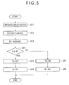
Fig. 5 is a flowchart showing an output process of a reference signal using the sampling-and-holding circuit. -
Fig. 6 is a graph showing an example of a contact detection using a first typical contact detector circuit. -
Fig. 7 is a graph showing an example of a contact detection using a second typical contact detector circuit. -
Fig. 8 is a block diagram showing a third typical contact detector circuit. -
Fig. 9 is a graph showing an example of a contact detection using the third typical contact detector circuit. - Exemplary embodiment(s) of the invention will be described below with reference to the attached drawings.
-
Fig. 1 is a schematic illustration of a contact sensor using a sensor signal detector according to an exemplary embodiment of the invention as acontact detector circuit 9. The contact sensor includes a stylus I having aspherical contact piece 3 at an end thereof. The stylus I also includes abalancer 4 for keeping an attitude of the stylus 1 at a base end thereof. The stylus 1 is held by astylus holder 2 approximately at a middle portion in an axial direction thereof. - A
piezoelectric element 5 that is configured to apply vibrations to the stylus 1 is attached approximately to the middle portion of the stylus 1. Thepiezoelectric element 5 includes avibration electrode 51 configured to apply vibrations to the stylus I and adetection electrode 52 configured to detect a contact of thecontact piece 3. A drive signal is sent to thevibration electrode 51 from adriver circuit 8. - The
detection electrode 52 generates a mechanical-electrical conversion output signal. The mechanical-electrical conversion output signal is detected by adetector circuit 6. An output signal of thedetector circuit 6 is sent to thedriver circuit 8 by a positive feedback. The feedback control excites thepiezoelectric element 5 at a predetermined resonance frequency. - The
detector circuit 6 outputs a detection output signal in a form of a sinusoidal signal of which amplitude decreases when thecontact piece 3 touches an object. Anamplitude filter circuit 7 detects the sinusoidal signal obtained by thedetection electrode 52 of thepiezoelectric element 5 of thedetector circuit 6, and extracts only amplitude information of the sinusoidal signal to output a DC sensor signal S. Theamplitude filter circuit 7 exemplarily includes a full-wave rectifier for converting AC (Alternating Current) into DC (Direct Current), and a smoothing circuit for smoothing an AC component remaining after a rectification. - The
contact detector circuit 9 detects a variation in a DC-level fluctuation component S3 (seeFigs. 2 and4 ) in the DC sensor signal S that rapidly decreases due to a contact with thecontact piece 3, and outputs a trigger signal TG. - Next, details of the arrangement of the
contact detector circuit 9 will be described below with reference to a block diagram shown inFig. 2 . - The
contact detector circuit 9 includes: a low-pass filter 21 (low-pass filter) into which the DC sensor signal S is inputted; a reference signal generation circuit 22 (reference signal generator) that converts a level of an output signal of the low-pass filter 21; a sampling-and-holding circuit (reference signal holder) 23 that samples and/or holds an output signal of the referencesignal generation circuit 22; and a trigger signal output circuit (trigger signal output unit) 24 that generates and outputs a trigger signal TG based on a result of a comparison between the DC sensor signal S and an output signal of the sampling-and-holdingcircuit 23. - The DC sensor signal S inputted to the low-
pass filter 21 is a composite signal in which a DC offset component S0, a low-frequency state change component S1 (representing variation due to temperature change and time-dependent change), a high-frequency noise component S2 and a DC-level fluctuation component S3 (a signal component caused when thecontact piece 3 touches an object), all of which are superimposed (i.e. S = S0 + S1 + S2 + S3). - The low-
pass filter 21 blocks the high-frequency noise component S2 and the DC-level fluctuation component S3 and passes only the DC offset component S0 and the low-frequency state change component S1 (i.e. S0 + S1) out of the components of the DC sensor signal S. - The reference
signal generation circuit 22 multiplies the output signal (SO + S1) with a coefficient K (0 < K < 1) to output a signal R1 = K(S0 + S1)). The signal R1 is selectively used as a later-described reference signal R. - It should be noted the value of the coefficient K is determined in consideration of a magnitude of the amplitude of the high-frequency noise component S2. Specifically, the coefficient K is determined so that the magnitude of ΔS = (1-K)S0 + S1) becomes greater than a maximum value of the amplitude (|S2|) of the high-frequency component S2, thereby achieving a highly accurate contact detection without being influenced by the high-frequency noise component S2.
- However, when the coefficient K is set excessively small, the trigger signal TG is generated at a timing different from an actual contact time between the
contact piece 3 and the object. Accordingly, the coefficient K is preferably set as large as possible as long as the contact detection is not influenced by the high-frequency noise component S2. - The sampling-and-holding
circuit 23 sequentially samples (acquires) the signal R1 = K(S0 + S1) when the trigger signal TG is not outputted from a later-described triggersignal output circuit 24 and sequentially outputs the obtained signal R1 as the reference signal R to the triggersignal output circuit 24. On the other hand, the sampling-and-holdingcircuit 23 holds a signal Rt1 when the trigger signal TG is started to be outputted, and keeps outputting the held signal to a comparator as the reference signal R while the trigger signal TG is kept on being outputted. In other words, the output signal of the sampling-and-holdingcircuit 23 the signal R1 (a variable value) when the trigger signal TG is not outputted, whereas the output signal becomes signal Rt I (a fixed value) when the trigger signal TG is outputted. - As shown in
Fig. 3 , the sampling-and-holdingcircuit 23 includes aswitch 231 and acapacitor 232. Theswitch 231 is configured to be set ON when the trigger signal TG is not outputted and to be set OFF when the trigger signal TG is outputted. - The sampling of the signal R1 by the sampling-and-holding
circuit 23 is performed when theswitch 231 is set ON. On the other hand, the reference signal R is held by the sampling-and-holdingcircuit 23 when theswitch 231 is set OFF. - When the
switch 231 is set OFF, an electric charge of thecapacitor 232 is held, where the output reference signal R is held at a value when theswitch 231 is set OFF irrespective of the variation in the signal R1 = K(S0 + S1) to be inputted. It should be noted that the sampling-and-holdingcircuit 23 is commercially available and the commercially available product can be directly used in this exemplary embodiment. - The trigger
signal output circuit 24 compares the DC sensor signal S (= S0 + S1 + S2 + S3) with the reference signal R (= Rlor Rt1) outputted from the sampling-and-holdingcircuit 23. When the DC sensor signal S is smaller than the reference signal R, the triggersignal output circuit 24 generates and outputs the trigger signal TG. - Next, an operation of the
contact detector circuit 9 of the exemplary embodiment will be described below with reference to a graph inFig. 4 and a flowchart inFig. 5 . - In this exemplary embodiment, it is exemplarily supposed that: the
contact piece 3 of the stylus 1 is initially separated from an object (not shown) (non-contact state); thecontact piece 3 then is brought into contact with the object and the contact state between thecontact piece 3 and the object is kept for a while; and thecontact piece 3 is again separated from the object (transitioning into the non-contact state). - In this instance, when the DC sensor signal S is inputted to the low-pass filter 21 (Step 1 (abbreviated as "ST1" [ST2, ST3...] in the drawings), the high-frequency noise component S2 and the (transitional) DC-level fluctuation component S3 are blocked so that only the DC offset component S0 and the low-frequency state change component S1 (i.e. signal (SO + S1)) are extracted to be outputted (Step 2). The reference
signal generation circuit 22 multiplies the output signal (S0 + S1) of the low-pass filter 21 with a coefficient K (Step 3) to output the signal R1 = K(S0 + S1). - In the period before a time t1 (Step 4: YES), the
contact piece 3 of the stylus 1 is not in contact with the object (non-contact state). Accordingly, the DC sensor signal S is greater than the reference signal R = R1. Since the trigger signal TG is not outputted during the non-contact state (S5) theswitch 231 is set ON, and the sequentially changing signal R1 = K(S0 + S1) is outputted as the reference signal R (Step 6). - Subsequently, when the
contact piece 3 is brought into contact with the object to run into a contact state, the DC sensor signal S rapidly decreases, so that the DC sensor signal S falls below the signal R1 at the time t1 (Step 4: YES → NO). Then, the trigger signal TG is outputted (Step 7), and the reference signal R is held by the sampling-and-holdingcircuit 23. As shown inFig. 4 , since the value of the signal R1 at the time t1 is Rt1, the reference signal R is held at the value Rt1 during the period from the time t1 to a time t2 (Step 8). - In other words, the reference signal R is switched from a variable value (signal R1) varying in accordance with an increase and decrease in the DC sensor signal S to a fixed value (signal Rt1) at the time t1. Since the contact state is kept in the period between the time t1 to the time t2, the reference signal R = Rt1 is compared with the DC sensor signal S.
- Subsequently, when the
contact piece 3 is out of contact with the object, the DC sensor signal S rapidly increases, so that the DC sensor signal S exceeds the signal R1 at the time t2 (Step 4: NO → YES). Then, since the output of the trigger signal TG is stopped (S5), theswitch 231 is set ON, and the signal R1 = K(S0 + S1) is again outputted from the sampling-and-holding circuit 23 (Step 6). In other words, the reference signal R is switched from the fixed value (signal Rt1) to the variable value (the signal R1) after the time t2. - As described above, in this exemplary embodiment, when the trigger signal TG is not outputted (i.e. in the non-contact state of the contact piece 3), the signal R1 (variable component) derived from the DC sensor signal S is used as the reference signal R, whereas the signal Rt1 (fixed value) is used as the reference signal R when the trigger signal TG is outputted (i.e. in the contact state of the contact piece 3). By thus switching the reference signals R, the contact/non-contact of the
contact piece 3 can be more accurately determined as compared to an instance where the variable signal R1 is kept being used as the reference signal R and an instance where the fixed value of the signal Rt1 is kept being used as the reference signal R. - Further, the fixed value of the signal R2 is set at the value of the reference signal R when the trigger signal TG is started to be outputted. The value of the reference signal R is set at the value of the signal R2 by being held at the value at the sampling-and-holding
circuit 23. The sampling-and-holdingcircuit 23 can be easily provided using theswitch 231 and thecapacitor 232 and also is commercially available. Accordingly, as compared with the arrangement disclosed in thePatent Literature 3 in which the signal R2 (= m·Rt1) is calculated with a software, the structure of thecontact detector circuit 9 can be simplified. - It should be understood that the scope of the present invention is not restricted to the above exemplary embodiment, but encompasses modification(s) and improvement(s) as long as such modification(s) and improvement(s) are compatible with an object of the invention.
- For instance, though the amplitude of the DC-level fluctuation component S3 decreases when a contact is detected in the above exemplary embodiment, the invention is also applicable to an instance where the amplitude or the like of the DC-level fluctuation component S3 increases when a contact is detected. It should be noted that, in such an instance, the value of the coefficient K has to be set greater than 1 (K > 1).
- Though the signal R1 is calculated by multiplying the output signal (SO + S1) of the low-
pass filter 21 with the coefficient K (i.e. R1 = K(S0 + S1)) in the above exemplary embodiment, the signal R1 may alternatively be calculated by subtracting a predetermined value L from the output signal (S0 + S1) of the low-pass filter 21 (i.e. R1 = S0 + S1 - L). - Though an instance in which the amplitude of the DC sensor signal S is extracted to detect a contact in a contact sensor using an ultrasonic touch trigger probe is exemplified in the above exemplary embodiment, the scope of the invention is not restricted thereto. For instance, the invention is applicable to an instance for detecting the frequency and/or phase of the DC sensor signal S to detect a contact based on the change in the frequency and/or phase. In other words, the invention is applicable to any sensor that employs a DC sensor signal S including a low-frequency state change component S1.
- Though the sampling-and-holding
circuit 23 in the above exemplary embodiment is provided by a hardware including theswitch 231 and thecapacitor 232, the sampling-and-holdingcircuit 23 may alternatively be provided by a software. - Though the
contact piece 3 in the above exemplary embodiment keeps in contact with the object for a while from an initial non-contact state, and subsequently returns to the non-contact state, the invention is also applicable to an instance in which thecontact piece 3 is not restored to the non-contact state from the contact state and is kept to be in the contact state for a long time. - Though the reference signal R is switched from the variable signal R1 to the signal Rt1 of the fixed value (Step 8) simultaneously with the output of the trigger signal TG (the time t1) (Step 7) in the above exemplary embodiment, it is not necessary that the signals are switched at the time t1 but may alternatively be switched at a predetermined time after the time t1.
- Similarly, though the reference signal R is switched from the signal Rt1 of the fixed value to the variable signal R1 (S6) simultaneously with the stop of the output of the trigger signal TG (the time t2) (S5) in the above exemplary embodiment, it is not necessary that the signals are switched at the time t2 but may alternatively be switched a predetermined time after the time t2.
- Though the sensor signal detector in the above exemplary embodiment is provided in a form of the
contact detector circuit 9, the invention may alternatively be provided in a form of a pressure detector circuit and an acceleration detector circuit.
Claims (4)
- A sensor signal detector (9) that is configured to detect a change in a change in a DC sensor signal (S) based on a change in a physical amount to be detected, the sensor signal detector (9) comprising:a reference signal generator (22) that is configured to generate a reference signal (K(S0 + S1)) from the DC sensor signal (S);a trigger signal output unit (24) that is configured to compare the DC sensor signal (S) with the reference signal and outputs a trigger signal (TG) based on a result of a comparison between the DC sensor signal and the reference signal; anda reference signal holder (23) that is configured to hold the reference signal when the trigger signal (TG) is started to be outputted, the held reference signal being outputted to the trigger signal output unit (24) while the trigger signal (TG) is outputted,the trigger signal output unit (24) using the reference signal outputted by the reference signal holder (23) for the comparison between the DC sensor signal (S) and the reference signal while the trigger signal (TG) is outputted.
- The sensor signal detector according to claim 1, wherein
the reference signal is held at the reference signal holder (23) by storing an electric charge in a capacitor (232) to hold a voltage. - The sensor signal detector according to claim 1 or 2, wherein
the DC sensor signal (S) comprises a DC-level fluctuation component (S3), a low-frequency state change component (S1) and a high-frequency noise component (S2) being superimposed with each other,
the sensor signal detector further comprises a low-pass filter (21) that is configured to receive the DC sensor signal (S) and block the high-frequency noise component (S2) and the DC-level fluctuation component (S3) in the received DC sensor signal (S) to output the low-frequency state change component (S1), and
the DC sensor signal (S) passing through the low-pass filter (21) is used for the comparison with the reference signal in the trigger signal output unit (24). - The sensor signal detector according to any one of claims 1 to 3, wherein
the DC sensor signal (S) is obtained by extracting amplitude information from a sinusoidal output signal of a touch signal probe driven by a piezoelectric element (5).
Applications Claiming Priority (1)
| Application Number | Priority Date | Filing Date | Title |
|---|---|---|---|
| JP2014125139A JP6418803B2 (en) | 2014-06-18 | 2014-06-18 | Sensor signal detection circuit |
Publications (2)
| Publication Number | Publication Date |
|---|---|
| EP2957856A1 true EP2957856A1 (en) | 2015-12-23 |
| EP2957856B1 EP2957856B1 (en) | 2016-08-17 |
Family
ID=53397958
Family Applications (1)
| Application Number | Title | Priority Date | Filing Date |
|---|---|---|---|
| EP15172160.2A Not-in-force EP2957856B1 (en) | 2014-06-18 | 2015-06-15 | Sensor signal detector |
Country Status (3)
| Country | Link |
|---|---|
| US (1) | US10006803B2 (en) |
| EP (1) | EP2957856B1 (en) |
| JP (1) | JP6418803B2 (en) |
Families Citing this family (3)
| Publication number | Priority date | Publication date | Assignee | Title |
|---|---|---|---|---|
| JP6393156B2 (en) * | 2014-11-06 | 2018-09-19 | 株式会社ミツトヨ | Shape measuring apparatus and shape measuring method |
| US20190299310A1 (en) * | 2018-03-30 | 2019-10-03 | Branson Ultrasonics Corporation | Contact Detection Based On Frequency In Ultrasonics |
| TWI779534B (en) * | 2020-03-25 | 2022-10-01 | 昇佳電子股份有限公司 | Capacitance sensing circuit |
Citations (5)
| Publication number | Priority date | Publication date | Assignee | Title |
|---|---|---|---|---|
| JPH06221806A (en) | 1992-12-03 | 1994-08-12 | Mitsutoyo Corp | Touch signal probe |
| GB2318232A (en) * | 1996-10-08 | 1998-04-15 | Mitutoyo Corp | Adaptive threshold circuit |
| JPH11223524A (en) * | 1998-02-05 | 1999-08-17 | Mitsutoyo Corp | Detection method and circuit for sudden fluctuation of level |
| WO2009112819A2 (en) * | 2008-03-11 | 2009-09-17 | Renishaw Plc | Touch trigger measurement probe |
| EP2120004A1 (en) * | 2008-05-15 | 2009-11-18 | Mitutoyo Corporation | Sensor signal detection circuit |
Family Cites Families (11)
| Publication number | Priority date | Publication date | Assignee | Title |
|---|---|---|---|---|
| US4531158A (en) * | 1982-01-27 | 1985-07-23 | Hitachi, Ltd. | Automatic focusing system for video cameras |
| JPS6147502A (en) * | 1984-08-13 | 1986-03-08 | Mitsutoyo Mfg Co Ltd | Touch signal detection circuit |
| JPS6151503A (en) * | 1984-08-21 | 1986-03-14 | Mitsutoyo Mfg Co Ltd | Touch signal detecting circuit |
| FR2673468A1 (en) * | 1991-02-28 | 1992-09-04 | Renishaw Plc | SIGNAL CONDITIONING CIRCUIT FOR A TRIGGERED PROBE. |
| AU4313200A (en) * | 2000-04-18 | 2001-10-30 | Alessandro Lana | Electronic sensor with an inertial system for detecting vibrations |
| JP4310026B2 (en) * | 2000-05-22 | 2009-08-05 | Okiセミコンダクタ株式会社 | Comparison circuit and demodulation circuit |
| JP3498908B2 (en) * | 2000-07-25 | 2004-02-23 | 株式会社ミツトヨ | AC signal amplitude sampling method and amplitude detection circuit |
| JP2002310727A (en) * | 2001-04-13 | 2002-10-23 | Mitsubishi Electric Corp | Abnormality detecting device and method for position detecting device |
| TW200509111A (en) * | 2003-08-27 | 2005-03-01 | Ricoh Co Ltd | The control of laser emission power for recording information on optical disc |
| JP2006220556A (en) * | 2005-02-10 | 2006-08-24 | Aichi Micro Intelligent Corp | Angle sensor |
| US7053806B1 (en) * | 2005-03-31 | 2006-05-30 | General Electric Company | System and method for calibration of autoranging architectures |
-
2014
- 2014-06-18 JP JP2014125139A patent/JP6418803B2/en not_active Expired - Fee Related
-
2015
- 2015-06-15 EP EP15172160.2A patent/EP2957856B1/en not_active Not-in-force
- 2015-06-16 US US14/740,707 patent/US10006803B2/en active Active
Patent Citations (7)
| Publication number | Priority date | Publication date | Assignee | Title |
|---|---|---|---|---|
| JPH06221806A (en) | 1992-12-03 | 1994-08-12 | Mitsutoyo Corp | Touch signal probe |
| GB2318232A (en) * | 1996-10-08 | 1998-04-15 | Mitutoyo Corp | Adaptive threshold circuit |
| JPH10111143A (en) | 1996-10-08 | 1998-04-28 | Mitsutoyo Corp | Detection circuit for change in dc level of sensor signal |
| JPH11223524A (en) * | 1998-02-05 | 1999-08-17 | Mitsutoyo Corp | Detection method and circuit for sudden fluctuation of level |
| WO2009112819A2 (en) * | 2008-03-11 | 2009-09-17 | Renishaw Plc | Touch trigger measurement probe |
| EP2120004A1 (en) * | 2008-05-15 | 2009-11-18 | Mitutoyo Corporation | Sensor signal detection circuit |
| JP2009276238A (en) | 2008-05-15 | 2009-11-26 | Mitsutoyo Corp | Sensor signal detection circuit |
Also Published As
| Publication number | Publication date |
|---|---|
| JP2016003979A (en) | 2016-01-12 |
| EP2957856B1 (en) | 2016-08-17 |
| JP6418803B2 (en) | 2018-11-07 |
| US10006803B2 (en) | 2018-06-26 |
| US20150369655A1 (en) | 2015-12-24 |
Similar Documents
| Publication | Publication Date | Title |
|---|---|---|
| EP2957856B1 (en) | Sensor signal detector | |
| CN103185850A (en) | Apparatus and method for detecting failure of switching device in inverter | |
| EP3460384A1 (en) | Measurement probe | |
| JP2889196B2 (en) | DC level change detection circuit for sensor signal | |
| EP2120004B1 (en) | Sensor signal detection circuit | |
| JP6218974B2 (en) | Acceleration sensor system and self-diagnosis method | |
| JP2011085483A (en) | Impedance measuring device | |
| JP5729323B2 (en) | Self-excited resonant circuit | |
| US10578661B2 (en) | Method for determining the quality factor of an oscillator | |
| JP2018072271A (en) | Self-excited resonance circuit | |
| JP2013022110A (en) | Needle thread tension measurement device of sewing machine | |
| US10845194B2 (en) | Inertial force detection device | |
| CN106104205B (en) | A method for optimizing the on-time of a Coriolis gyroscope and a Coriolis gyroscope suitable for this | |
| US10704952B2 (en) | System and method for measuring vibration on a machine | |
| JP5060168B2 (en) | Rotational vibration phase detection apparatus and method | |
| US20150020593A1 (en) | Apparatus for driving inertial sensor and controlling method of the same | |
| JP2010017023A (en) | Power failure detection device | |
| JP6450559B2 (en) | Measuring apparatus, measuring method and program | |
| JP4178941B2 (en) | Method of creating conversion table for distance detection and displacement sensor | |
| KR101109378B1 (en) | Resonant frequency measurement method of cantilever biosensor | |
| JP2019207192A (en) | Material testing machine | |
| JP6136590B2 (en) | Control device for vibration carrying device and vibration carrying device | |
| JP3138717U (en) | Resonant frequency detector | |
| JP2016099288A (en) | Measurement device and measurement range switch-over method | |
| JP5781902B2 (en) | Signal level measuring circuit and displacement measuring device having the same |
Legal Events
| Date | Code | Title | Description |
|---|---|---|---|
| PUAI | Public reference made under article 153(3) epc to a published international application that has entered the european phase |
Free format text: ORIGINAL CODE: 0009012 |
|
| AK | Designated contracting states |
Kind code of ref document: A1 Designated state(s): AL AT BE BG CH CY CZ DE DK EE ES FI FR GB GR HR HU IE IS IT LI LT LU LV MC MK MT NL NO PL PT RO RS SE SI SK SM TR |
|
| AX | Request for extension of the european patent |
Extension state: BA ME |
|
| 17P | Request for examination filed |
Effective date: 20160121 |
|
| RBV | Designated contracting states (corrected) |
Designated state(s): AL AT BE BG CH CY CZ DE DK EE ES FI FR GB GR HR HU IE IS IT LI LT LU LV MC MK MT NL NO PL PT RO RS SE SI SK SM TR |
|
| GRAP | Despatch of communication of intention to grant a patent |
Free format text: ORIGINAL CODE: EPIDOSNIGR1 |
|
| INTG | Intention to grant announced |
Effective date: 20160308 |
|
| GRAS | Grant fee paid |
Free format text: ORIGINAL CODE: EPIDOSNIGR3 |
|
| GRAA | (expected) grant |
Free format text: ORIGINAL CODE: 0009210 |
|
| AK | Designated contracting states |
Kind code of ref document: B1 Designated state(s): AL AT BE BG CH CY CZ DE DK EE ES FI FR GB GR HR HU IE IS IT LI LT LU LV MC MK MT NL NO PL PT RO RS SE SI SK SM TR |
|
| REG | Reference to a national code |
Ref country code: GB Ref legal event code: FG4D |
|
| REG | Reference to a national code |
Ref country code: CH Ref legal event code: EP |
|
| REG | Reference to a national code |
Ref country code: IE Ref legal event code: FG4D |
|
| REG | Reference to a national code |
Ref country code: AT Ref legal event code: REF Ref document number: 821525 Country of ref document: AT Kind code of ref document: T Effective date: 20160915 |
|
| REG | Reference to a national code |
Ref country code: DE Ref legal event code: R096 Ref document number: 602015000204 Country of ref document: DE |
|
| REG | Reference to a national code |
Ref country code: NL Ref legal event code: MP Effective date: 20160817 |
|
| REG | Reference to a national code |
Ref country code: LT Ref legal event code: MG4D |
|
| REG | Reference to a national code |
Ref country code: AT Ref legal event code: MK05 Ref document number: 821525 Country of ref document: AT Kind code of ref document: T Effective date: 20160817 |
|
| PG25 | Lapsed in a contracting state [announced via postgrant information from national office to epo] |
Ref country code: LT Free format text: LAPSE BECAUSE OF FAILURE TO SUBMIT A TRANSLATION OF THE DESCRIPTION OR TO PAY THE FEE WITHIN THE PRESCRIBED TIME-LIMIT Effective date: 20160817 Ref country code: IT Free format text: LAPSE BECAUSE OF FAILURE TO SUBMIT A TRANSLATION OF THE DESCRIPTION OR TO PAY THE FEE WITHIN THE PRESCRIBED TIME-LIMIT Effective date: 20160817 Ref country code: FI Free format text: LAPSE BECAUSE OF FAILURE TO SUBMIT A TRANSLATION OF THE DESCRIPTION OR TO PAY THE FEE WITHIN THE PRESCRIBED TIME-LIMIT Effective date: 20160817 Ref country code: RS Free format text: LAPSE BECAUSE OF FAILURE TO SUBMIT A TRANSLATION OF THE DESCRIPTION OR TO PAY THE FEE WITHIN THE PRESCRIBED TIME-LIMIT Effective date: 20160817 Ref country code: HR Free format text: LAPSE BECAUSE OF FAILURE TO SUBMIT A TRANSLATION OF THE DESCRIPTION OR TO PAY THE FEE WITHIN THE PRESCRIBED TIME-LIMIT Effective date: 20160817 Ref country code: NL Free format text: LAPSE BECAUSE OF FAILURE TO SUBMIT A TRANSLATION OF THE DESCRIPTION OR TO PAY THE FEE WITHIN THE PRESCRIBED TIME-LIMIT Effective date: 20160817 Ref country code: NO Free format text: LAPSE BECAUSE OF FAILURE TO SUBMIT A TRANSLATION OF THE DESCRIPTION OR TO PAY THE FEE WITHIN THE PRESCRIBED TIME-LIMIT Effective date: 20161117 |
|
| PG25 | Lapsed in a contracting state [announced via postgrant information from national office to epo] |
Ref country code: ES Free format text: LAPSE BECAUSE OF FAILURE TO SUBMIT A TRANSLATION OF THE DESCRIPTION OR TO PAY THE FEE WITHIN THE PRESCRIBED TIME-LIMIT Effective date: 20160817 Ref country code: LV Free format text: LAPSE BECAUSE OF FAILURE TO SUBMIT A TRANSLATION OF THE DESCRIPTION OR TO PAY THE FEE WITHIN THE PRESCRIBED TIME-LIMIT Effective date: 20160817 Ref country code: GR Free format text: LAPSE BECAUSE OF FAILURE TO SUBMIT A TRANSLATION OF THE DESCRIPTION OR TO PAY THE FEE WITHIN THE PRESCRIBED TIME-LIMIT Effective date: 20161118 Ref country code: PL Free format text: LAPSE BECAUSE OF FAILURE TO SUBMIT A TRANSLATION OF THE DESCRIPTION OR TO PAY THE FEE WITHIN THE PRESCRIBED TIME-LIMIT Effective date: 20160817 Ref country code: SE Free format text: LAPSE BECAUSE OF FAILURE TO SUBMIT A TRANSLATION OF THE DESCRIPTION OR TO PAY THE FEE WITHIN THE PRESCRIBED TIME-LIMIT Effective date: 20160817 Ref country code: AT Free format text: LAPSE BECAUSE OF FAILURE TO SUBMIT A TRANSLATION OF THE DESCRIPTION OR TO PAY THE FEE WITHIN THE PRESCRIBED TIME-LIMIT Effective date: 20160817 Ref country code: PT Free format text: LAPSE BECAUSE OF FAILURE TO SUBMIT A TRANSLATION OF THE DESCRIPTION OR TO PAY THE FEE WITHIN THE PRESCRIBED TIME-LIMIT Effective date: 20161219 |
|
| PG25 | Lapsed in a contracting state [announced via postgrant information from national office to epo] |
Ref country code: EE Free format text: LAPSE BECAUSE OF FAILURE TO SUBMIT A TRANSLATION OF THE DESCRIPTION OR TO PAY THE FEE WITHIN THE PRESCRIBED TIME-LIMIT Effective date: 20160817 Ref country code: RO Free format text: LAPSE BECAUSE OF FAILURE TO SUBMIT A TRANSLATION OF THE DESCRIPTION OR TO PAY THE FEE WITHIN THE PRESCRIBED TIME-LIMIT Effective date: 20160817 |
|
| REG | Reference to a national code |
Ref country code: DE Ref legal event code: R097 Ref document number: 602015000204 Country of ref document: DE |
|
| PG25 | Lapsed in a contracting state [announced via postgrant information from national office to epo] |
Ref country code: CZ Free format text: LAPSE BECAUSE OF FAILURE TO SUBMIT A TRANSLATION OF THE DESCRIPTION OR TO PAY THE FEE WITHIN THE PRESCRIBED TIME-LIMIT Effective date: 20160817 Ref country code: BE Free format text: LAPSE BECAUSE OF FAILURE TO SUBMIT A TRANSLATION OF THE DESCRIPTION OR TO PAY THE FEE WITHIN THE PRESCRIBED TIME-LIMIT Effective date: 20160817 Ref country code: BG Free format text: LAPSE BECAUSE OF FAILURE TO SUBMIT A TRANSLATION OF THE DESCRIPTION OR TO PAY THE FEE WITHIN THE PRESCRIBED TIME-LIMIT Effective date: 20161117 Ref country code: SK Free format text: LAPSE BECAUSE OF FAILURE TO SUBMIT A TRANSLATION OF THE DESCRIPTION OR TO PAY THE FEE WITHIN THE PRESCRIBED TIME-LIMIT Effective date: 20160817 Ref country code: DK Free format text: LAPSE BECAUSE OF FAILURE TO SUBMIT A TRANSLATION OF THE DESCRIPTION OR TO PAY THE FEE WITHIN THE PRESCRIBED TIME-LIMIT Effective date: 20160817 Ref country code: SM Free format text: LAPSE BECAUSE OF FAILURE TO SUBMIT A TRANSLATION OF THE DESCRIPTION OR TO PAY THE FEE WITHIN THE PRESCRIBED TIME-LIMIT Effective date: 20160817 |
|
| PLBE | No opposition filed within time limit |
Free format text: ORIGINAL CODE: 0009261 |
|
| STAA | Information on the status of an ep patent application or granted ep patent |
Free format text: STATUS: NO OPPOSITION FILED WITHIN TIME LIMIT |
|
| 26N | No opposition filed |
Effective date: 20170518 |
|
| PG25 | Lapsed in a contracting state [announced via postgrant information from national office to epo] |
Ref country code: SI Free format text: LAPSE BECAUSE OF FAILURE TO SUBMIT A TRANSLATION OF THE DESCRIPTION OR TO PAY THE FEE WITHIN THE PRESCRIBED TIME-LIMIT Effective date: 20160817 |
|
| PG25 | Lapsed in a contracting state [announced via postgrant information from national office to epo] |
Ref country code: MC Free format text: LAPSE BECAUSE OF FAILURE TO SUBMIT A TRANSLATION OF THE DESCRIPTION OR TO PAY THE FEE WITHIN THE PRESCRIBED TIME-LIMIT Effective date: 20160817 |
|
| REG | Reference to a national code |
Ref country code: IE Ref legal event code: MM4A |
|
| REG | Reference to a national code |
Ref country code: FR Ref legal event code: ST Effective date: 20180228 |
|
| PG25 | Lapsed in a contracting state [announced via postgrant information from national office to epo] |
Ref country code: LU Free format text: LAPSE BECAUSE OF NON-PAYMENT OF DUE FEES Effective date: 20170615 Ref country code: IE Free format text: LAPSE BECAUSE OF NON-PAYMENT OF DUE FEES Effective date: 20170615 |
|
| PG25 | Lapsed in a contracting state [announced via postgrant information from national office to epo] |
Ref country code: FR Free format text: LAPSE BECAUSE OF NON-PAYMENT OF DUE FEES Effective date: 20170630 |
|
| PG25 | Lapsed in a contracting state [announced via postgrant information from national office to epo] |
Ref country code: MT Free format text: LAPSE BECAUSE OF NON-PAYMENT OF DUE FEES Effective date: 20170615 |
|
| PG25 | Lapsed in a contracting state [announced via postgrant information from national office to epo] |
Ref country code: AL Free format text: LAPSE BECAUSE OF FAILURE TO SUBMIT A TRANSLATION OF THE DESCRIPTION OR TO PAY THE FEE WITHIN THE PRESCRIBED TIME-LIMIT Effective date: 20160817 |
|
| REG | Reference to a national code |
Ref country code: CH Ref legal event code: PL |
|
| PG25 | Lapsed in a contracting state [announced via postgrant information from national office to epo] |
Ref country code: LI Free format text: LAPSE BECAUSE OF NON-PAYMENT OF DUE FEES Effective date: 20180630 Ref country code: CH Free format text: LAPSE BECAUSE OF NON-PAYMENT OF DUE FEES Effective date: 20180630 |
|
| PG25 | Lapsed in a contracting state [announced via postgrant information from national office to epo] |
Ref country code: HU Free format text: LAPSE BECAUSE OF FAILURE TO SUBMIT A TRANSLATION OF THE DESCRIPTION OR TO PAY THE FEE WITHIN THE PRESCRIBED TIME-LIMIT; INVALID AB INITIO Effective date: 20150615 |
|
| PG25 | Lapsed in a contracting state [announced via postgrant information from national office to epo] |
Ref country code: CY Free format text: LAPSE BECAUSE OF FAILURE TO SUBMIT A TRANSLATION OF THE DESCRIPTION OR TO PAY THE FEE WITHIN THE PRESCRIBED TIME-LIMIT Effective date: 20160817 |
|
| PG25 | Lapsed in a contracting state [announced via postgrant information from national office to epo] |
Ref country code: MK Free format text: LAPSE BECAUSE OF FAILURE TO SUBMIT A TRANSLATION OF THE DESCRIPTION OR TO PAY THE FEE WITHIN THE PRESCRIBED TIME-LIMIT Effective date: 20160817 |
|
| PG25 | Lapsed in a contracting state [announced via postgrant information from national office to epo] |
Ref country code: TR Free format text: LAPSE BECAUSE OF FAILURE TO SUBMIT A TRANSLATION OF THE DESCRIPTION OR TO PAY THE FEE WITHIN THE PRESCRIBED TIME-LIMIT Effective date: 20160817 |
|
| PG25 | Lapsed in a contracting state [announced via postgrant information from national office to epo] |
Ref country code: IS Free format text: LAPSE BECAUSE OF FAILURE TO SUBMIT A TRANSLATION OF THE DESCRIPTION OR TO PAY THE FEE WITHIN THE PRESCRIBED TIME-LIMIT Effective date: 20161217 |
|
| PGFP | Annual fee paid to national office [announced via postgrant information from national office to epo] |
Ref country code: DE Payment date: 20230620 Year of fee payment: 9 |
|
| PGFP | Annual fee paid to national office [announced via postgrant information from national office to epo] |
Ref country code: GB Payment date: 20230622 Year of fee payment: 9 |
|
| REG | Reference to a national code |
Ref country code: DE Ref legal event code: R119 Ref document number: 602015000204 Country of ref document: DE |
|
| GBPC | Gb: european patent ceased through non-payment of renewal fee |
Effective date: 20240615 |
|
| PG25 | Lapsed in a contracting state [announced via postgrant information from national office to epo] |
Ref country code: DE Free format text: LAPSE BECAUSE OF NON-PAYMENT OF DUE FEES Effective date: 20250101 |
|
| PG25 | Lapsed in a contracting state [announced via postgrant information from national office to epo] |
Ref country code: GB Free format text: LAPSE BECAUSE OF NON-PAYMENT OF DUE FEES Effective date: 20240615 |