EP2956986B1 - Phase shift device - Google Patents
Phase shift device Download PDFInfo
- Publication number
- EP2956986B1 EP2956986B1 EP14707670.7A EP14707670A EP2956986B1 EP 2956986 B1 EP2956986 B1 EP 2956986B1 EP 14707670 A EP14707670 A EP 14707670A EP 2956986 B1 EP2956986 B1 EP 2956986B1
- Authority
- EP
- European Patent Office
- Prior art keywords
- phase shift
- shift device
- pieces
- signal electrode
- tunable
- Prior art date
- Legal status (The legal status is an assumption and is not a legal conclusion. Google has not performed a legal analysis and makes no representation as to the accuracy of the status listed.)
- Active
Links
Images


Classifications
-
- H—ELECTRICITY
- H01—ELECTRIC ELEMENTS
- H01P—WAVEGUIDES; RESONATORS, LINES, OR OTHER DEVICES OF THE WAVEGUIDE TYPE
- H01P1/00—Auxiliary devices
- H01P1/18—Phase-shifters
- H01P1/184—Strip line phase-shifters
-
- H—ELECTRICITY
- H01—ELECTRIC ELEMENTS
- H01G—CAPACITORS; CAPACITORS, RECTIFIERS, DETECTORS, SWITCHING DEVICES, LIGHT-SENSITIVE OR TEMPERATURE-SENSITIVE DEVICES OF THE ELECTROLYTIC TYPE
- H01G7/00—Capacitors in which the capacitance is varied by non-mechanical means; Processes of their manufacture
- H01G7/06—Capacitors in which the capacitance is varied by non-mechanical means; Processes of their manufacture having a dielectric selected for the variation of its permittivity with applied voltage, i.e. ferroelectric capacitors
-
- H—ELECTRICITY
- H01—ELECTRIC ELEMENTS
- H01P—WAVEGUIDES; RESONATORS, LINES, OR OTHER DEVICES OF THE WAVEGUIDE TYPE
- H01P1/00—Auxiliary devices
- H01P1/18—Phase-shifters
- H01P1/181—Phase-shifters using ferroelectric devices
-
- H—ELECTRICITY
- H01—ELECTRIC ELEMENTS
- H01Q—ANTENNAS, i.e. RADIO AERIALS
- H01Q13/00—Waveguide horns or mouths; Slot antennas; Leaky-waveguide antennas; Equivalent structures causing radiation along the transmission path of a guided wave
- H01Q13/10—Resonant slot antennas
- H01Q13/106—Microstrip slot antennas
-
- H—ELECTRICITY
- H01—ELECTRIC ELEMENTS
- H01Q—ANTENNAS, i.e. RADIO AERIALS
- H01Q9/00—Electrically-short antennas having dimensions not more than twice the operating wavelength and consisting of conductive active radiating elements
- H01Q9/04—Resonant antennas
- H01Q9/0407—Substantially flat resonant element parallel to ground plane, e.g. patch antenna
- H01Q9/045—Substantially flat resonant element parallel to ground plane, e.g. patch antenna with particular feeding means
- H01Q9/0457—Substantially flat resonant element parallel to ground plane, e.g. patch antenna with particular feeding means electromagnetically coupled to the feed line
Definitions
- the present invention relates a phase shift device with at least one tunable component.
- This phase shift is frequency independent (phase shifter) or frequency dependent (variable delay line).
- radio frequency is meant a rate of oscillation in the range of about 3 kHz to 300 GHz, which corresponds to the frequency of radio waves and of the alternating currents which carry and transmit radio signals.
- phase shift devices like e.g. semiconductors, MEMS or tunable dielectrics to design agile RF components.
- Phase shift devices are one of the key elements for reconfigurable electronic beam steering antennas.
- Microwave components such as phase shift devices can be formed from microstrip lines.
- a microstrip line is a type of electrical planar transmission line which can be fabricated using printed circuit board technology. It consists of a conducting strip shaped electrode that is separated from a planar ground electrode by a dielectric layer known as the substrate.
- the substrate can be formed by liquid crystal polymers (LCPs).
- LCPs liquid crystal polymers
- the LCP material is not tunable with respect to the relative permittivity of this material. Therefore, due to the lack of tunable characteristic features that are relevant for the configuration of a tunable RF device, making use of LCPs is not convenient for designing of a tunable device such as a varactor.
- Liquid crystals exhibits features and properties of conventional liquids as well as of solid crystals. For instance, an LC may flow like a liquid, but its molecules may be orientated in a crystal-like way. In contrast to liquid crystal polymers (LCPs), the relative permittivity of liquid crystals (LCs) may be affected by e.g. a voltage applied to the LC material.
- LCPs liquid crystal polymers
- coplanar waveguides have been loaded with shunt LC varactors.
- the tuning speed of such an LC devices is affected by its topology.
- One of the known drawbacks of such devices is the high metallic loss of the CPW.
- the varactors were implemented by patches as floating electrodes bridging the center conductor and the ground plane. This results in reduced tuning efficiency and high insertion loss of such an artificial transmission line.
- Prior art [9] discloses a phase shift device comprising a planar transmission line that is formed by a signal electrode and a ground electrode which are separated by a dielectric substance, and further comprising a tunable dielectric material, the signal electrode of the planar transmission line is divided into several pieces and comprises overlapping areas of adjacent pieces that are filled with a dielectric material, forming a varactor, namely a dielectric tunable component with a metal-insulator-metal type capacitor.
- a varactor namely a dielectric tunable component with a metal-insulator-metal type capacitor
- the invention relates to a phase shift device comprising a planar transmission line that is formed by a signal electrode and a ground electrode which are separated by a dielectric substance, and further comprising a tunable dielectric material, whereby the signal electrode of the planar transmission line is divided into several pieces and comprises overlapping areas of adjacent pieces, thereby forming a dielectric tunable component (varactor) with a metal-insulator-metal type capacitor, characterized in that the overlapping areas of adjacent pieces of the planar transmission line are filled with the tunable dielectric material.
- a transmission line is formed by two electrodes: A signal electrode and a ground electrode.
- the material of the electrodes is preferably low resistive RF electrode material such as Ag, Cu or Au. Other materials or alloys with similar conductive properties are possible.
- the signal electrode is divided into several pieces along the length, i.e. along the propagation direction. These pieces are e.g. implemented as top side pieces on the top side of bottom glass and as bottom side pieces on the bottom side of top glass.
- the top glass and the bottom glass are stacked in such a way that a in plan view, i.e. when viewed perpendicular to the propagation of the signal a continuous signal electrode is formed.
- the terms top glass and bottom glass do not indicate that other suitable materials are waived.
- each overlapping area forms a metal-insulator-metal type capacitor.
- the insulator is the tunable liquid crystal material
- this area forms a dielectric tunable component (varactor). This tunable component enables to construct this phase shift device in a very compact way.
- the varactors Due to LC technology, the varactors feature low losses compared to other technologies such as semiconductors for frequencies higher than 5 GHz preferably frequencies higher than 10 GHz. Additionally, since microstrip line is used, the phase shifter losses would be much less than compared to [6,7].
- the several pieces of the signal electrode are arranged at two or more different distance levels with respect to the ground electrode. Arrangement of the several pieces of the signal electrode at two different levels allows for easy and cost-saving fabrication of such a device, as the two different levels can be on two surfaces of substrate layers. Three or more different distance levels allow for complex configurations and e.g. different layers of LC material that is located between two adjacent distance levels.
- the tunable liquid crystal material can be arranged as a single and continuous layer between several pieces of the signal electrode that are arranged at two different distance levels.
- the boundaries of this continuous, i.e. unbroken layer can be adapted and limited to the shape and extension of the signal electrode that is defined as a composed covering of the several pieces.
- This continuous layer can completely cover the usually larger ground electrode.
- the continuous layer can be arranged between two adjacent layers of either electrodes or substrate layers and completely fill a cavity between those dielectric substrate layers. This allows for fast and cheap fabrication of such an arrangement e.g. by use of well-established liquid crystal display technology.
- the tunable liquid crystal material in order to save tunable liquid crystal material or to allow for separate control of confined spatial regions of the tunable liquid crystal material it is possible to arrange the tunable liquid crystal material as several confined layer areas between the overlapping areas of adjacent pieces of the signal electrode at two different distance levels.
- the pieces of the signal electrode are arranged in a straight line.
- the transmission line may be meandered, e.g. in an N-shape or in spiral shape. This allows for a transmission line length that is much longer than the physical dimension of the phase shift device.
- the phase shift along the transmission line is exclusively or at least predominantly due to the tunable varactors that are of the metal-insulator-metal capacitor type and that are arranged along the signal electrode.
- the configuration, shape and arrangement of the pieces of the signal electrode should not result in resonant structures that significantly affects the time delay for the signal propagation along the transmission line.
- a phase shift device can be characterized in that the signal electrode is divided into several pieces along the length of the transmission line, whereby said several pieces are alternatingly implemented as top side pieces on the top side and as bottom side pieces on the bottom side of a non-tunable dielectric substrate and whereby at some sections there are overlapping areas between an top side piece and an adjacent bottom side piece of the signal electrode, and whereby these overlapping areas are filled with a tunable liquid crystal material and these overlapping areas form a dielectric tunable component (varactor) with a metal-insulator-metal type capacitor.
- a LC mixture is used, whose relative dielectric constant is continuously tunable between 2.4 and 3.2 by application of a tuning voltage and surface alignment method.
- the maximum dielectric loss tangent tan ⁇ of this material is less than 0.006 for all tuning states.
- the LC layer (from metal to metal) is specified to 3 ⁇ m to obtain a fast response time that is less than 25 ms.
- the device provides for a 367° differential phase shift at 20 GHz with 6.1 dB insertion loss at maximum.
- FoM frequency-dependent figure of merit
- the FoM of the exemplary embodiment is 60°/dB at 20 GHz.
- the planar transmission line comprises at least two serially connected dielectric tunable components that are connected by a non-overlapping section of the signal electrode.
- the signal transmission along the planar transmission line is dominantly and basically solely affected be the number and configuration of the varactors, i.e. the tunable dielectric components that are arranged along the signal electrode.
- the phase shift is easily controlled and modified by application of a tuning bias voltage to the tunable liquid crystal material that forms the tunable dielectric material between the overlapping areas of adjacent pieces of the signal electrode, i.e. the parallel plate like tunable capacitor that acts as the varactor.
- the tuning is performed by control electrodes. These electrodes operate as control element. These electrodes transmit the different bias voltages to drive the varactors through bias lines.
- the bias lines are preferably made of a low conductive material in order not to affect the RF circuitry. For this purpose, low conductive electrodes can be used since they become transparent for the RF signal. Typical materials for the bias lines are preferably ITO (indium tin oxide), NiCr (nickel chromium) or some other alloys having a conductivity of less than 10e5 S/m.
- the phase shift device is combined with a radiating element to transmit the RF signal.
- a radiating element are also referred to as patch antennas.
- the radiating elements and the feed lines are usually photoetched on the dielectric substrate.
- the radiating elements, i.e. the patch antennas are configured as square, rectangular, thin strip (dipole), circular, elliptical, triangular, or any other formation.
- the radiating element is an arbitrarily shaped microstrip patch antenna or a microstrip slot antenna.
- LC Liquid crystals
- LC can be employed as a tunable dielectric, specifically optimized LC mixtures offer high performance at microwave frequencies with a loss tangent below 0.006.
- the relative tunability defined as the ratio of the tuning range of the minimum permittivity to the maximum permittivity, is preferably between 5% and 30% or between 10% and 25% or between 15% and 30% or between 5% and 14%.
- LC based planar phase shift devices are usually customized depending on desired antenna performance.
- the phase shift device is configured and adapted in order to reduce insertion loss, to increase beam steering speed and to allow for wide range scans.
- a LC mixture optimized for RF applications is used.
- a possibility to realize tunable RF components with LC is presented in Fig. 3 . It shows the cross section of an inverted microstrip line using LC as a tunable substrate for different bias voltages.
- the setup consists of two stacked substrates, the top one carrying the microstrip line and the lower one the ground plane. In between the two substrates, a thin LC layer is encapsulated.
- phase shift device can be combined with a radiating element e.g. in order to provide for phased array antenna.
- planar transmission line and the antenna are coupled by using an aperture coupling method.
- planar transmission line and the antenna are coupled by using a proximity coupling method.
- planar transmission line and the antenna are coupled directly, e.g. using a inset-fed technique or through an vertical interconnect.
- liquid crystal (LC) materials are anisotropic. This property stems from the rod-like shape of the molecules, as shown in an example structure of a typical LC molecule in Fig. 1 . Here it is shown how the phase configuration of a LC material changes with increasing temperature. Together with the molecule in Fig. 1 the corresponding anisotropic dielectric properties are indicated. Since the material is liquid, the molecules feature only a weak molecular adhesion, and thus their orientation in the bulk can be changed. Owing to the rod-like shape, the molecules in a bulk tend to orient themselves in parallel order.
- the relative permittivity parallel to the molecule long axis is denoted as ⁇ r,
- liquid crystal material If such a liquid crystal material is arranged between a signal electrode and a ground electrode of a strip shaped transmission line, the transmission speed of a radio frequency signal along the transmission line will be affected by the permittivity of the liquid crystal material.
- An electric field can be generated e.g. by application of a control voltage to the liquid crystal material and will affect the orientation of the rod-like shaped liquid crystal molecules.
- a control voltage to affect the orientation of the rod-like shaped liquid crystal molecules.
- Fig. 2 shows a prior art planar transmission line formed as a microstrip line. It consist of a ground electrode 1 and a continuous, i.e. unbroken signal electrode 2 which are separated by a layer of a dielectric substrate 3. The propagation direction is along the direction of the signal electrode 2 and indicated by an arrow.
- Figures 3a, 3b and 3c show a perspective view, a cross-section view and a schematic representation of main components of a phase shift device line according to the invention. It comprises a ground electrode 1 and a signal electrode 2 which form a planar transmission line.
- the signal electrode 2 is composed of several pieces 4 and 5 of low resistive RF electrode material that are arranged at two different distance levels perpendicular to and with respect to the ground electrode 1.
- the several pieces 4, 5 are aligned along the transmission line, i.e. the signal propagation path as defined by the direction of the signal electrode 2 and indicated by an arrow.
- the several pieces 4, 5 of the signal electrode 2 are arranged with respect to each other in order to create overlapping areas 6 of adjacent pieces 4, 5.
- a layer of the non-tunable dielectric substrate 3 preferably glass.
- the space between the several pieces 4, 5 of the signal electrode 2 is filled with a tunable liquid crystal material 7. Between each adjacent pieces 4, 5 there are overlapping areas 6.
- the pieces 4, 5 are stacked and arranged in such a manner that apparently a continuous signal electrode 2 is formed when viewed from the top view, i.e. perpendicular to the ground electrode 1.
- On top of the tunable liquid crystal 7 is a second layer 3' of a non-tunable dielectric substrate.
- the several pieces 4, 5 of the signal electrode 2 can be e.g. printed or coated or laminated onto the corresponding surfaces of the layers 3 and 3' of the non-tunable dielectric substrate.
- the pieces 4, 5 of the signal electrode 2 are connected with control elements 8 (only shown in Figures 3b and 3c ) that consist of a low conductive material, preferably ITO (indium tin oxide), which is transparent for RF.
- control elements 8 transmit the bias voltage that can be applied in order to tune the liquid crystal material 7 in the overlapping areas 6, i.e. in order to modify the relative permittivity of the liquid crystal material 7 that is between the overlapping areas 6 of adjacent pieces 4, 5 of the signal electrode 2 which affects the transmission properties of a RF signal that is transmitted along the planar transmission line.
- the time delay of signal transmission along the planar transmission line i.e. the phase shift of a signal that is transmitted along the transmission line of the phase shift device according to the invention is generated by the successive time delays for each signal jump between the adjacent pieces 4, 5 of the signal electrode 2 that are arranged at different distance levels with respect to the ground electrode 1.
- the total time delay mainly depends on the number of signal jumps during the propagation of the signal along the planar transmission line.
- Each single jump causes a certain time delay that can be modified by tuning the tunable liquid crystal material 7 at the corresponding overlapping area 6.
- the total time delay is the small time delay of a single jump multiplied by the number of jumps along the planar transmission line.
- the planar transmission line of the phase shift device comprises at least two but preferably many serially connected dielectric tunable components (varactors) that are connected by a non-overlapping section of the signal electrode 2.
- a schematic representation of the planar transmission line is shown in Fig. 3d .
- Figures 4a and 4b show a more detailed cross-section view and a corresponding schematic representation of a single varactor configuration, i.e. the overlapping area 6 between two adjacent pieces 4, 5 of the signal electrode 2 and the ground electrode 1 in the phase shift device as shown in Figures 3a to 3d .
- Figures 5, 6 and 7 show different embodiments for a radiation element comprising a phase shift device according to Figures 3a to 3d that is coupled with an antenna patch 9.
- Fig. 5 the several pieces 4, 5 of the signal electrode 2 of the planar transmission line and the antenna patch 9 are coupled by using an aperture coupling method.
- the antenna patch 9 is separated from the ground electrode 1 by a layer 10 of a non-tunable dielectric substrate.
- the energy that is transmitted along the transmission line, i.e. along the signal electrode 2 and ground electrode 1 is coupled to the antenna patch 9 through a nearby slot 11 within the ground electrode 1.
- planar transmission line and the antenna patch 9 are coupled by using a proximity coupling method.
- planar transmission line and the antenna patch 9 are coupled by using an insert feed coupling method.
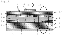
- Fig. 8 shows a different embodiment of the phase shift device according to the invention.
- some additional pieces 12 of the several pieces 4, 5 and 12 are arranged at a third distance level with respect to the ground electrode 1.
- the additional pieces 12 are mounted on another surface of the layer 3' of the non-tunable dielectric substrate that is opposed to the surface on which the pieces 5 of the second distance level are mounted.
- the time delay for a signal jump between the additional pieces 12 and the adjacent pieces 5 cannot be modified, as the layer 3' that separates the second distance level with pieces 5 from the third distance level with additional pieces 5 is made of a non-tunable dielectric substrate.
- the additional signal jumps will add a fixed time delay that only depends on the number of these signal jumps, resulting in e.g. an offset that can be manufactured in a very cost-saving manner.
- the sequence of overlapping pieces at three different distance levels may differ and e.g. a first piece 4 on the lowest distance level may overlap with a subsequent piece 12 on the highest distance level, followed by another piece on the middle distance level.
- the RF signal then jumps from the lowest distance level to the highest distance level and subsequently to a middle level and back to the lowest level.
- the respective signal jumps that each cause a certain time delay can be predetermined and arranged in many different ways, resulting in the total phase shift of the signal.
- a skilled person in art can also electrically connect some pieces on different distance levels through vertical interconnects as well.
- a second layer of a tunable dielectric material between the several pieces 4, 5 and the additional pieces 12 of the signal electrode 2.
- Such a second layer may consist of a completely different tunable dielectric material or of the same liquid crystal material that is used for the first layer of the tunable liquid crystal material 7.
- the time delay for signals jumps between the second and the third distance level may by controlled differently and result in many more possibilities for controlling the phase shift device and the resulting phase shift.
Landscapes
- Engineering & Computer Science (AREA)
- Power Engineering (AREA)
- Physics & Mathematics (AREA)
- Electromagnetism (AREA)
- Microelectronics & Electronic Packaging (AREA)
- Waveguide Switches, Polarizers, And Phase Shifters (AREA)
- Waveguide Aerials (AREA)
- Waveguides (AREA)
Description
- The present invention relates a phase shift device with at least one tunable component. This phase shift is frequency independent (phase shifter) or frequency dependent (variable delay line).
- The shortage in the available frequency spectrum for radio communications and the requirement for more functionality in smaller volume increase the demand for reconfigurable components. Hereinafter radio frequency (RF) is meant a rate of oscillation in the range of about 3 kHz to 300 GHz, which corresponds to the frequency of radio waves and of the alternating currents which carry and transmit radio signals. Depending on the device requirements there are different possible solutions for phase shift devices like e.g. semiconductors, MEMS or tunable dielectrics to design agile RF components.
- Phase shift devices are one of the key elements for reconfigurable electronic beam steering antennas.
- From the state of the art the following documents are cited as examples of the above mentioned phase shift devices:
- 1. US patent
US 8,305,259 B2 - 2. US patent
US 8,022,861 B2 - 3. US patent
US 8,013,688 B2 - 4.
PCT patent application WO 2012/123072 A1 - 5. US patent application
US 2009/0302976 A1 - 6. F. Goelden, A. Gaebler, M. Goebel, A. Manabe, S. Mueller, and R. Jakoby, "Tunable liquid crystal phase shifter for microwave frequencies,"Electronics Letters, vol. 45, no. 13, pp. 686-687, 2009.
- 7. O. H. Karabey, F. Goelden, A. Gaebler, S. Strunck, and R. Jakoby, ".
- 8. US patent application
US 5,936,484 A - 9. Japanese patent application
JP 2003/008310 A - 10. Onur Hamza Karabey et al., "Continuously Polarization Agile Antenna by Using Liquid Crystal-Based Tunable Variable Delay Lines", IEEE vol. 61, no. 1, 1. January 2013, pages 70-76, ISSN: 0018-926X
- 11. US patent application
US 2009/073332 A1 - 12. US patent application
US 2002/051334 A1 - Microwave components such as phase shift devices can be formed from microstrip lines. A microstrip line is a type of electrical planar transmission line which can be fabricated using printed circuit board technology. It consists of a conducting strip shaped electrode that is separated from a planar ground electrode by a dielectric layer known as the substrate.
- As in [1, 3], the substrate can be formed by liquid crystal polymers (LCPs). However, the LCP material is not tunable with respect to the relative permittivity of this material. Therefore, due to the lack of tunable characteristic features that are relevant for the configuration of a tunable RF device, making use of LCPs is not convenient for designing of a tunable device such as a varactor.
- Liquid crystals (LCs) exhibits features and properties of conventional liquids as well as of solid crystals. For instance, an LC may flow like a liquid, but its molecules may be orientated in a crystal-like way. In contrast to liquid crystal polymers (LCPs), the relative permittivity of liquid crystals (LCs) may be affected by e.g. a voltage applied to the LC material.
- In prior art [6], coplanar waveguides (CPW) have been loaded with shunt LC varactors. The tuning speed of such an LC devices is affected by its topology. One of the known drawbacks of such devices is the high metallic loss of the CPW. Additionally, due to the CPW, the varactors were implemented by patches as floating electrodes bridging the center conductor and the ground plane. This results in reduced tuning efficiency and high insertion loss of such an artificial transmission line.
- Similarly in [7], the tuning efficiency of the LC varactors is improved by using a parallel plate capacitor topology. However, there a slotline was loaded with these LC varactors in shunts. Indeed, loading a microstrip line results in higher performance because microstrip lines feature system-inherently low losses.
- Prior art [9] discloses a phase shift device comprising a planar transmission line that is formed by a signal electrode and a ground electrode which are separated by a dielectric substance, and further comprising a tunable dielectric material, the signal electrode of the planar transmission line is divided into several pieces and comprises overlapping areas of adjacent pieces that are filled with a dielectric material, forming a varactor, namely a dielectric tunable component with a metal-insulator-metal type capacitor. However, due to the arrangement of the tunable dielectric material within the dielectric tunable component the response time and performance are limited.
- Therefore it is the task of the invention to reduce disadvantages of phase shift devices according to prior art and to provide for a favorable phase shift device with low response time as well as with a high performance, that comprises both features simultaneously in a compact and planar configuration.
- The invention relates to a phase shift device comprising a planar transmission line that is formed by a signal electrode and a ground electrode which are separated by a dielectric substance, and further comprising a tunable dielectric material, whereby the signal electrode of the planar transmission line is divided into several pieces and comprises overlapping areas of adjacent pieces, thereby forming a dielectric tunable component (varactor) with a metal-insulator-metal type capacitor, characterized in that the overlapping areas of adjacent pieces of the planar transmission line are filled with the tunable dielectric material.
- A transmission line (microstrip line) is formed by two electrodes: A signal electrode and a ground electrode. The material of the electrodes is preferably low resistive RF electrode material such as Ag, Cu or Au. Other materials or alloys with similar conductive properties are possible. The signal electrode is divided into several pieces along the length, i.e. along the propagation direction. These pieces are e.g. implemented as top side pieces on the top side of bottom glass and as bottom side pieces on the bottom side of top glass. The top glass and the bottom glass are stacked in such a way that a in plan view, i.e. when viewed perpendicular to the propagation of the signal a continuous signal electrode is formed. The terms top glass and bottom glass do not indicate that other suitable materials are waived. Additionally, there are some sections where the top side pieces and the bottom side pieces of the signal electrode are overlapping. At least, these overlapping areas between the two glasses and the top side piece and the respective bottom side piece of the signal electrode are filled with a tunable liquid crystal material. Therefore, each overlapping area forms a metal-insulator-metal type capacitor. In this case, since the insulator is the tunable liquid crystal material, this area forms a dielectric tunable component (varactor). This tunable component enables to construct this phase shift device in a very compact way.
- Due to LC technology, the varactors feature low losses compared to other technologies such as semiconductors for frequencies higher than 5 GHz preferably frequencies higher than 10 GHz. Additionally, since microstrip line is used, the phase shifter losses would be much less than compared to [6,7].
- According to an embodiment of the invention the several pieces of the signal electrode are arranged at two or more different distance levels with respect to the ground electrode. Arrangement of the several pieces of the signal electrode at two different levels allows for easy and cost-saving fabrication of such a device, as the two different levels can be on two surfaces of substrate layers. Three or more different distance levels allow for complex configurations and e.g. different layers of LC material that is located between two adjacent distance levels.
- The tunable liquid crystal material can be arranged as a single and continuous layer between several pieces of the signal electrode that are arranged at two different distance levels. The boundaries of this continuous, i.e. unbroken layer can be adapted and limited to the shape and extension of the signal electrode that is defined as a composed covering of the several pieces. This continuous layer can completely cover the usually larger ground electrode. For many applications the continuous layer can be arranged between two adjacent layers of either electrodes or substrate layers and completely fill a cavity between those dielectric substrate layers. This allows for fast and cheap fabrication of such an arrangement e.g. by use of well-established liquid crystal display technology.
- However, in order to save tunable liquid crystal material or to allow for separate control of confined spatial regions of the tunable liquid crystal material it is possible to arrange the tunable liquid crystal material as several confined layer areas between the overlapping areas of adjacent pieces of the signal electrode at two different distance levels.
- For most applications arranging the pieces of the signal electrode parallel to the propagation direction, e.g. linearly along the propagation direction of a radio frequency signal is advantageous, since this prevents any discontinues, resulting in less losses. If required or feasible, the pieces of the signal electrode are arranged in a straight line.
- However, for some applications that require many varactors along the transmission line, the transmission line may be meandered, e.g. in an N-shape or in spiral shape. This allows for a transmission line length that is much longer than the physical dimension of the phase shift device.
- The phase shift along the transmission line is exclusively or at least predominantly due to the tunable varactors that are of the metal-insulator-metal capacitor type and that are arranged along the signal electrode. The configuration, shape and arrangement of the pieces of the signal electrode should not result in resonant structures that significantly affects the time delay for the signal propagation along the transmission line.
- A phase shift device according to an embodiment of the invention can be characterized in that the signal electrode is divided into several pieces along the length of the transmission line, whereby said several pieces are alternatingly implemented as top side pieces on the top side and as bottom side pieces on the bottom side of a non-tunable dielectric substrate and whereby at some sections there are overlapping areas between an top side piece and an adjacent bottom side piece of the signal electrode, and whereby these overlapping areas are filled with a tunable liquid crystal material and these overlapping areas form a dielectric tunable component (varactor) with a metal-insulator-metal type capacitor.
- In a exemplary embodiment the non-tunable dielectric substrate that supports the several pieces of the signal electrode is chosen to be a 700 µm thick borofloat glass from Schott AG with εr,glass = 4.6 and its loss tangent tanδ = 0.0037 at 25°C and at 1 MHz. A LC mixture is used, whose relative dielectric constant is continuously tunable between 2.4 and 3.2 by application of a tuning voltage and surface alignment method. The maximum dielectric loss tangent tan δ of this material is less than 0.006 for all tuning states. The LC layer (from metal to metal) is specified to 3 µm to obtain a fast response time that is less than 25 ms. The device provides for a 367° differential phase shift at 20 GHz with 6.1 dB insertion loss at maximum.
- An important parameter for quantifying the RF performance of these devices is a frequency-dependent figure of merit (FoM). This is defined by the ratio of the maximum differential phase shift and the highest insertion loss over all tuning states.
- Hence, the FoM of the exemplary embodiment is 60°/dB at 20 GHz.
- In a further embodiment the planar transmission line comprises at least two serially connected dielectric tunable components that are connected by a non-overlapping section of the signal electrode. The signal transmission along the planar transmission line is dominantly and basically solely affected be the number and configuration of the varactors, i.e. the tunable dielectric components that are arranged along the signal electrode. The phase shift is easily controlled and modified by application of a tuning bias voltage to the tunable liquid crystal material that forms the tunable dielectric material between the overlapping areas of adjacent pieces of the signal electrode, i.e. the parallel plate like tunable capacitor that acts as the varactor.
- The tuning is performed by control electrodes. These electrodes operate as control element. These electrodes transmit the different bias voltages to drive the varactors through bias lines. The bias lines are preferably made of a low conductive material in order not to affect the RF circuitry. For this purpose, low conductive electrodes can be used since they become transparent for the RF signal. Typical materials for the bias lines are preferably ITO (indium tin oxide), NiCr (nickel chromium) or some other alloys having a conductivity of less than 10e5 S/m.
- In further embodiments the phase shift device is combined with a radiating element to transmit the RF signal. Often radiating element are also referred to as patch antennas. The radiating elements and the feed lines are usually photoetched on the dielectric substrate. The radiating elements, i.e. the patch antennas are configured as square, rectangular, thin strip (dipole), circular, elliptical, triangular, or any other formation.
- In further embodiments the radiating element is an arbitrarily shaped microstrip patch antenna or a microstrip slot antenna.
- Liquid crystals (LC) are suitable to realize tunable RF devices. LC can be employed as a tunable dielectric, specifically optimized LC mixtures offer high performance at microwave frequencies with a loss tangent below 0.006. The relative tunability, defined as the ratio of the tuning range of the minimum permittivity to the maximum permittivity, is preferably between 5% and 30% or between 10% and 25% or between 15% and 30% or between 5% and 14%.
- LC based planar phase shift devices are usually customized depending on desired antenna performance. For this purpose the phase shift device is configured and adapted in order to reduce insertion loss, to increase beam steering speed and to allow for wide range scans. According to this invention, a LC mixture optimized for RF applications is used. A possibility to realize tunable RF components with LC is presented in
Fig. 3 . It shows the cross section of an inverted microstrip line using LC as a tunable substrate for different bias voltages. The setup consists of two stacked substrates, the top one carrying the microstrip line and the lower one the ground plane. In between the two substrates, a thin LC layer is encapsulated. - The phase shift device according to the invention can be combined with a radiating element e.g. in order to provide for phased array antenna.
- In a first embodiment of such a combination the planar transmission line and the antenna are coupled by using an aperture coupling method. In a second embodiment the planar transmission line and the antenna are coupled by using a proximity coupling method. In a third embodiment the planar transmission line and the antenna are coupled directly, e.g. using a inset-fed technique or through an vertical interconnect.
- The various objects and characteristics of the invention will emerge more clearly in the description which follows and which describes non-limiting embodiments of the invention, as well as in the attached figures which represent:
-
Fig. 1 , a schematic view of a typical LC molecule and its temperature dependency -
Fig. 2 , a schematic view of a planar transmission line according to prior art -
Fig. 3a to 3d , a schematic perspective view, a cross-sectional view and a topside view of a phase shift device with several LC varactors according to the invention and a schematic representation of tunable LC varactors that are arranged within the signal electrode of the phase shift device, -
Fig. 4a and 4b , a cross-sectional enlarged view of a single overlapping area of adjacent pieces of the signal electrode within the phase shift device according toFigures 3a to 3d , and a schematic representation of the LC varactor shown inFig. 4a , -
Fig. 5 , a schematic cross-section view of a first embodiment of the phase shift device with a coupled antenna, -
Fig. 6 , a schematic cross-section view of a second embodiment of the phase shift device with a coupled antenna, -
Fig. 7 , a schematic cross-section view of a third embodiment of the phase shift device with a coupled antenna, and -
Fig. 8 , a schematic cross-section view of a different configuration of the phase shift device according toFigures 3a to 3d , whereby the several pieces of the signal electrode are arranged on three different distance levels with respect to the ground electrode. - In general liquid crystal (LC) materials are anisotropic. This property stems from the rod-like shape of the molecules, as shown in an example structure of a typical LC molecule in
Fig. 1 . Here it is shown how the phase configuration of a LC material changes with increasing temperature. Together with the molecule inFig. 1 the corresponding anisotropic dielectric properties are indicated. Since the material is liquid, the molecules feature only a weak molecular adhesion, and thus their orientation in the bulk can be changed. Owing to the rod-like shape, the molecules in a bulk tend to orient themselves in parallel order. The relative permittivity parallel to the molecule long axis is denoted as εr,| | and perpendicular to the long axis as εr,∟. - If such a liquid crystal material is arranged between a signal electrode and a ground electrode of a strip shaped transmission line, the transmission speed of a radio frequency signal along the transmission line will be affected by the permittivity of the liquid crystal material.
- With these two permittivities εr, | | and εr,∟ the loss tangents tan δ, | | and tan δ,∟ for the signal transmission are associated.
- An electric field can be generated e.g. by application of a control voltage to the liquid crystal material and will affect the orientation of the rod-like shaped liquid crystal molecules. Thus, by application of a predetermined control voltage the relative permittivity of the liquid crystal material can be controlled.
- There are other tunable dielectric materials with similar properties, i.e. with a tunable relative permittivity that can be controlled and adjusted by application of an electric field. It will be well understood by a person skilled in the art that even though the following description focuses on tunable liquid crystal material, many different materials with tunable relative permittivity can be used for the purpose of this invention and are included.
-
Fig. 2 shows a prior art planar transmission line formed as a microstrip line. It consist of aground electrode 1 and a continuous, i.e.unbroken signal electrode 2 which are separated by a layer of adielectric substrate 3. The propagation direction is along the direction of thesignal electrode 2 and indicated by an arrow. -
Figures 3a, 3b and 3c show a perspective view, a cross-section view and a schematic representation of main components of a phase shift device line according to the invention. It comprises aground electrode 1 and asignal electrode 2 which form a planar transmission line. Thesignal electrode 2 is composed ofseveral pieces ground electrode 1. Theseveral pieces signal electrode 2 and indicated by an arrow. Theseveral pieces signal electrode 2 are arranged with respect to each other in order to create overlappingareas 6 ofadjacent pieces - Between the ground and the signal electrode is a layer of the non-tunable
dielectric substrate 3, preferably glass. The space between theseveral pieces signal electrode 2 is filled with a tunableliquid crystal material 7. Between eachadjacent pieces areas 6. Thepieces continuous signal electrode 2 is formed when viewed from the top view, i.e. perpendicular to theground electrode 1. On top of the tunableliquid crystal 7 is a second layer 3' of a non-tunable dielectric substrate. Theseveral pieces signal electrode 2 can be e.g. printed or coated or laminated onto the corresponding surfaces of thelayers 3 and 3' of the non-tunable dielectric substrate. - The
pieces signal electrode 2 are connected with control elements 8 (only shown inFigures 3b and 3c ) that consist of a low conductive material, preferably ITO (indium tin oxide), which is transparent for RF. Thesecontrol elements 8 transmit the bias voltage that can be applied in order to tune theliquid crystal material 7 in the overlappingareas 6, i.e. in order to modify the relative permittivity of theliquid crystal material 7 that is between the overlappingareas 6 ofadjacent pieces signal electrode 2 which affects the transmission properties of a RF signal that is transmitted along the planar transmission line. - The time delay of signal transmission along the planar transmission line, i.e. the phase shift of a signal that is transmitted along the transmission line of the phase shift device according to the invention is generated by the successive time delays for each signal jump between the
adjacent pieces signal electrode 2 that are arranged at different distance levels with respect to theground electrode 1. - Contrary to the phase shift devices of prior art that comprise a layer of tunable LC material between the
ground electrode 1 and the microstrip like signal electrode 2 (e.g. similar toFig. 2 ), the total time delay mainly depends on the number of signal jumps during the propagation of the signal along the planar transmission line. Each single jump causes a certain time delay that can be modified by tuning the tunableliquid crystal material 7 at the corresponding overlappingarea 6. The total time delay is the small time delay of a single jump multiplied by the number of jumps along the planar transmission line. - Accordingly, the planar transmission line of the phase shift device according to the invention comprises at least two but preferably many serially connected dielectric tunable components (varactors) that are connected by a non-overlapping section of the
signal electrode 2. A schematic representation of the planar transmission line is shown inFig. 3d . -
Figures 4a and 4b show a more detailed cross-section view and a corresponding schematic representation of a single varactor configuration, i.e. the overlappingarea 6 between twoadjacent pieces signal electrode 2 and theground electrode 1 in the phase shift device as shown inFigures 3a to 3d . -
Figures 5, 6 and 7 show different embodiments for a radiation element comprising a phase shift device according toFigures 3a to 3d that is coupled with anantenna patch 9. - In
Fig. 5 theseveral pieces signal electrode 2 of the planar transmission line and theantenna patch 9 are coupled by using an aperture coupling method. For such a coupling theantenna patch 9 is separated from theground electrode 1 by alayer 10 of a non-tunable dielectric substrate. The energy that is transmitted along the transmission line, i.e. along thesignal electrode 2 andground electrode 1 is coupled to theantenna patch 9 through anearby slot 11 within theground electrode 1. - In
Fig 6 the planar transmission line and theantenna patch 9 are coupled by using a proximity coupling method. - In
Fig 7 the planar transmission line and theantenna patch 9 are coupled by using an insert feed coupling method. -
Fig. 8 shows a different embodiment of the phase shift device according to the invention. Other than previously described, in addition to theseveral pieces signal electrode 2 that are arranged at two different distance levels, someadditional pieces 12 of theseveral pieces ground electrode 1. Theadditional pieces 12 are mounted on another surface of the layer 3' of the non-tunable dielectric substrate that is opposed to the surface on which thepieces 5 of the second distance level are mounted. - With the exemplary embodiment of
Figure 8 , the time delay for a signal jump between theadditional pieces 12 and theadjacent pieces 5 cannot be modified, as the layer 3' that separates the second distance level withpieces 5 from the third distance level withadditional pieces 5 is made of a non-tunable dielectric substrate. Hence there is no dielectric tunable varactor wherever an overlappingarea 6 exist betweenpieces 5 andadditional pieces 12. Therefore, in order to be able to tune the phase shift it might be advantageous to achieve an overlapping area between 12 and 4. Nevertheless, the additional signal jumps will add a fixed time delay that only depends on the number of these signal jumps, resulting in e.g. an offset that can be manufactured in a very cost-saving manner. - In yet another embodiment of the phase shift device that differs from the one shown in
Fig. 8 , the sequence of overlapping pieces at three different distance levels may differ and e.g. afirst piece 4 on the lowest distance level may overlap with asubsequent piece 12 on the highest distance level, followed by another piece on the middle distance level. The RF signal then jumps from the lowest distance level to the highest distance level and subsequently to a middle level and back to the lowest level. It will be understood that the respective signal jumps that each cause a certain time delay can be predetermined and arranged in many different ways, resulting in the total phase shift of the signal. A skilled person in art can also electrically connect some pieces on different distance levels through vertical interconnects as well. - It is also possible to add a second layer of a tunable dielectric material between the
several pieces additional pieces 12 of thesignal electrode 2. Such a second layer may consist of a completely different tunable dielectric material or of the same liquid crystal material that is used for the first layer of the tunableliquid crystal material 7. Even when the second layer equals the first layer ofliquid crystal material 7, by use of different control elements or by application of a different bias voltage the time delay for signals jumps between the second and the third distance level may by controlled differently and result in many more possibilities for controlling the phase shift device and the resulting phase shift. - It is also possible to arrange the
several pieces signal electrode 2 at more than two or three distance levels with respect to theground electrode 1. -
- 1
- ground electrode
- 2
- signal electrode
- 3
- layer of non-tunable dielectric substrate
- 4
- pieces of
signal electrode 2 at lower distance level - 5
- pieces of
signal electrode 2 at higher distance level - 6
- overlapping area
- 7
- tunable liquid crystal material
- 8
- control element
- 9
- antenna patch
- 10
- layer of non-tunable dielectric substrate
- 11
- slot
- 12
- additional pieces of
signal electrode 2
Claims (17)
- Phase shift device comprising a planar transmission line that is formed by a signal electrode (2) and a ground electrode (1) which are separated by a dielectric substance, and further comprising a tunable dielectric material (7), whereby the signal electrode (2) of the planar transmission line is divided into several pieces (4, 5) and comprises overlapping areas (6) of adjacent pieces (4, 5), thereby forming a dielectric tunable component (varactor) with a metal-insulator-metal type capacitor, characterized in that the overlapping areas (6) of adjacent pieces (4, 5) of the planar transmission line are filled with the tunable dielectric material (7).
- Phase shift device according to claim 1, characterized in that the tunable dielectric material (7) is a liquid crystal material.
- Phase shift device according to claim 1 or claim 2, characterized in that the several pieces (4, 5) of the signal electrode (2) are arranged at two or more different distance levels with respect to the ground electrode (1).
- Phase shift device according to claim 3, characterized in that the tunable dielectric material (7) is arranged as a single and continuous layer between several pieces (4, 5) of the signal electrode (2) that are arranged at two different distance levels.
- Phase shift device according to claim 3, characterized in that the tunable dielectric material (7) is arranged as at least several confined layer areas between the overlapping areas (6) of adjacent pieces (4, 5) of the signal electrode (2) at two different distance levels.
- Phase shift device according to one of the preceding claims, characterized in that the pieces (4, 5) of the signal electrode (2) are linearly arranged along the propagation direction of a radio frequency signal.
- Phase shift device according to one of the preceding claims, characterized in that the pieces (4, 5) of the signal electrode (2) are arranged in a straight line.
- A phase shift device according to one of the preceding claims, characterized in that the signal electrode (2) is divided into several pieces (4, 5) along the length of the transmission line, whereby said several pieces (4, 5) are alternatingly implemented as top side pieces (5) on the top side and as bottom side pieces (4) on the bottom side of a non-tunable dielectric substrate and whereby at some sections there are overlapping areas (6) between an top side piece (5) and an adjacent bottom side piece (4) of the signal electrode (2), and whereby these overlapping areas (6) are filled with a tunable liquid crystal material (7) and these overlapping areas (6) form a dielectric tunable component (varactor) with a metal-insulator-metal type capacitor.
- Phase shift device according to one of the preceding claims, characterized in that the planar transmission line comprises at least two serially connected dielectric tunable components that are connected by a non-overlapping section of the signal electrode (2).
- Phase shift device according to one of the preceding claims, characterized in that it comprises liquid crystal material (7) with tunability of relative permittivity, defined as the ratio of the tuning range of the permittivity to the maximum permittivity between 5% and 30%.
- Phase shift device according to one of the preceding claims, characterized in that it comprises at least one control element (8) that is connected with some of the pieces (4, 5) of the signal electrode (2) and that transmit a bias voltage in order to tune the liquid crystal material (7) in the overlapping areas (6).
- Phase shift device according to claim 11, characterized in that the at least one control element (8) consists of ITO (indium-tin-oxide).
- Phase shift device according to one of the preceding claims, characterized in that the planar transmission line is coupled with a radiating element.
- Phase shift device according to claim 13, characterized in that the radiating element is an arbitrary shaped microstrip patch antenna (9) or microstrip slot antenna.
- Phase shift device according to one of the claims 13 or 14, characterized in that the planar transmission line and the radiating element are coupled by using an aperture coupling method.
- Phase shift device according to one of the claims 13 or 14, characterized in that the planar transmission line and the radiating element are coupled by using a proximity coupling method.
- Phase shift device according to one of the claims 13 to 16, characterized in that planar transmission line and the radiating element can be connected directly, e.g. using a inset-fed technique or through an vertical interconnect.
Priority Applications (1)
| Application Number | Priority Date | Filing Date | Title |
|---|---|---|---|
| EP14707670.7A EP2956986B1 (en) | 2013-02-15 | 2014-02-14 | Phase shift device |
Applications Claiming Priority (3)
| Application Number | Priority Date | Filing Date | Title |
|---|---|---|---|
| EP13155432.1A EP2768072A1 (en) | 2013-02-15 | 2013-02-15 | Phase shifting device |
| PCT/EP2014/052964 WO2014125095A1 (en) | 2013-02-15 | 2014-02-14 | Phase shift device |
| EP14707670.7A EP2956986B1 (en) | 2013-02-15 | 2014-02-14 | Phase shift device |
Publications (2)
| Publication Number | Publication Date |
|---|---|
| EP2956986A1 EP2956986A1 (en) | 2015-12-23 |
| EP2956986B1 true EP2956986B1 (en) | 2017-02-01 |
Family
ID=47715909
Family Applications (2)
| Application Number | Title | Priority Date | Filing Date |
|---|---|---|---|
| EP13155432.1A Withdrawn EP2768072A1 (en) | 2013-02-15 | 2013-02-15 | Phase shifting device |
| EP14707670.7A Active EP2956986B1 (en) | 2013-02-15 | 2014-02-14 | Phase shift device |
Family Applications Before (1)
| Application Number | Title | Priority Date | Filing Date |
|---|---|---|---|
| EP13155432.1A Withdrawn EP2768072A1 (en) | 2013-02-15 | 2013-02-15 | Phase shifting device |
Country Status (7)
| Country | Link |
|---|---|
| US (2) | US10141620B2 (en) |
| EP (2) | EP2768072A1 (en) |
| JP (1) | JP6362624B2 (en) |
| KR (1) | KR102326919B1 (en) |
| CN (1) | CN105308789B (en) |
| ES (1) | ES2623252T3 (en) |
| WO (1) | WO2014125095A1 (en) |
Cited By (6)
| Publication number | Priority date | Publication date | Assignee | Title |
|---|---|---|---|---|
| EP3609017A1 (en) | 2018-08-06 | 2020-02-12 | ALCAN Systems GmbH | Radio frequency phase shifting device |
| DE102018119508A1 (en) * | 2018-08-10 | 2020-02-13 | Alcan Systems Gmbh | Group antenna made of a dielectric material |
| EP3664215A1 (en) | 2018-12-07 | 2020-06-10 | ALCAN Systems GmbH | Radio frequency phase shifting device |
| US10854970B2 (en) | 2018-11-06 | 2020-12-01 | Alcan Systems Gmbh | Phased array antenna |
| US10862182B2 (en) | 2018-08-06 | 2020-12-08 | Alcan Systems Gmbh | RF phase shifter comprising a differential transmission line having overlapping sections with tunable dielectric material for phase shifting signals |
| WO2021152438A1 (en) * | 2020-01-30 | 2021-08-05 | Nokia Solutions And Networks Oy | Apparatus comprising a transmission line for radio frequency signals |
Families Citing this family (87)
| Publication number | Priority date | Publication date | Assignee | Title |
|---|---|---|---|---|
| EP2768072A1 (en) * | 2013-02-15 | 2014-08-20 | Technische Universität Darmstadt | Phase shifting device |
| US9755286B2 (en) * | 2014-12-05 | 2017-09-05 | Huawei Technologies Co., Ltd. | System and method for variable microwave phase shifter |
| JP6554224B2 (en) * | 2016-02-16 | 2019-07-31 | シャープ株式会社 | Scanning antenna |
| US10811784B2 (en) * | 2016-03-01 | 2020-10-20 | Kymeta Corporation | Broadband RF radial waveguide feed with integrated glass transition |
| US10535923B2 (en) * | 2016-03-22 | 2020-01-14 | Elwha Llc | Systems and methods for reducing intermodulation for electronically controlled adaptive antenna arrays |
| US10411349B2 (en) | 2016-03-22 | 2019-09-10 | Elwha Llc | Systems and methods for reducing intermodulation for electronically controlled adaptive antenna arrays |
| CN105914470B (en) * | 2016-05-03 | 2019-01-25 | 上海交通大学 | Liquid crystal patch antenna with variable electrical tuning range and method of making and using the same |
| US11109451B2 (en) | 2016-07-20 | 2021-08-31 | Kymeta Corporation | Internal heater for RF apertures |
| CN106154603B (en) * | 2016-07-29 | 2019-12-06 | 合肥工业大学 | Liquid crystal phase-shifting unit and phase-controlled antenna formed by same |
| US10326205B2 (en) * | 2016-09-01 | 2019-06-18 | Wafer Llc | Multi-layered software defined antenna and method of manufacture |
| US10199710B2 (en) * | 2016-09-01 | 2019-02-05 | Wafer Llc | Variable dielectric constant-based devices |
| CN106773338B (en) * | 2017-01-16 | 2020-02-18 | 京东方科技集团股份有限公司 | A liquid crystal microwave phase shifter |
| CN106684551B (en) | 2017-01-24 | 2019-07-23 | 京东方科技集团股份有限公司 | A phase shifting unit, antenna array, display panel and display device |
| WO2018143536A1 (en) * | 2017-01-31 | 2018-08-09 | Samsung Electronics Co., Ltd. | Liquid crystal-based high-frequency device and high-frequency switch |
| RU2653084C1 (en) * | 2017-01-31 | 2018-05-07 | Самсунг Электроникс Ко., Лтд. | High-frequency device based on liquid crystals |
| CN206602182U (en) * | 2017-04-06 | 2017-10-31 | 京东方科技集团股份有限公司 | A kind of antenna structure and communication apparatus |
| CN106961008B (en) * | 2017-04-06 | 2019-03-29 | 京东方科技集团股份有限公司 | Antenna structure and driving method and antenna system |
| CN106932933B (en) * | 2017-05-09 | 2019-08-27 | 京东方科技集团股份有限公司 | A liquid crystal antenna and its manufacturing method |
| US10651549B2 (en) | 2017-07-06 | 2020-05-12 | Innolux Corporation | Microwave device |
| CN109216902B (en) * | 2017-07-06 | 2021-03-16 | 群创光电股份有限公司 | Microwave device |
| US10705391B2 (en) * | 2017-08-30 | 2020-07-07 | Wafer Llc | Multi-state control of liquid crystals |
| US10332687B2 (en) | 2017-10-23 | 2019-06-25 | Blackberry Limited | Tunable coplanar capacitor with vertical tuning and lateral RF path and methods for manufacturing thereof |
| US10497774B2 (en) | 2017-10-23 | 2019-12-03 | Blackberry Limited | Small-gap coplanar tunable capacitors and methods for manufacturing thereof |
| US11233310B2 (en) * | 2018-01-29 | 2022-01-25 | The Boeing Company | Low-profile conformal antenna |
| CN108321541B (en) * | 2018-02-22 | 2021-10-15 | 京东方科技集团股份有限公司 | Antenna structure and its driving method and communication device |
| CN108398816B (en) * | 2018-03-26 | 2020-12-29 | 北京京东方专用显示科技有限公司 | A liquid crystal phase shifter and its manufacturing method and phase shifting method |
| CN108539331B (en) * | 2018-04-13 | 2021-01-15 | 合肥工业大学 | Terahertz slotting phase-shifting unit based on liquid crystal and phased array antenna formed by same |
| CN108598631B (en) * | 2018-04-19 | 2020-10-23 | 合肥工业大学 | Reflective double-layer liquid crystal phase-shifting unit based on patterned graphene electrode |
| CN110416668A (en) * | 2018-04-26 | 2019-11-05 | 北京超材信息科技有限公司 | A kind of liquid crystal phase shifter |
| CA3101948A1 (en) * | 2018-05-01 | 2019-11-07 | Wafer Llc | Low cost dielectric for electrical transmission and antenna using same |
| CN108493592B (en) * | 2018-05-03 | 2019-12-20 | 京东方科技集团股份有限公司 | Microstrip antenna, preparation method thereof and electronic equipment |
| DE102018112069A1 (en) * | 2018-05-18 | 2019-11-21 | Schott Ag | Use of a flat glass in electronic components |
| CN110518311B (en) * | 2018-05-21 | 2025-01-28 | 京东方科技集团股份有限公司 | Phase shifter and working method thereof, antenna, and communication device |
| US12224471B2 (en) | 2018-05-21 | 2025-02-11 | Beijing Boe Optoelectronics Technology Co., Ltd. | Liquid crystal phase shifter having a first electrode with periodic metal patches and a second electrode with a one-piece microstrip |
| WO2019223647A1 (en) | 2018-05-21 | 2019-11-28 | 京东方科技集团股份有限公司 | Phase shifter and operation method therefor, antenna, and communication device |
| CN108711669B (en) | 2018-05-28 | 2021-04-23 | 京东方科技集团股份有限公司 | A frequency tunable antenna and method of making the same |
| CN108615966B (en) * | 2018-05-28 | 2020-06-30 | 京东方科技集团股份有限公司 | Antenna and method of making the same |
| CN108563050B (en) * | 2018-05-31 | 2020-10-30 | 成都天马微电子有限公司 | Liquid crystal phase shifter and antenna |
| CN108490270B (en) * | 2018-07-02 | 2020-01-24 | 京东方科技集团股份有限公司 | Measuring device, measuring system and measuring method for liquid crystal dielectric constant |
| CN108615962B (en) | 2018-07-18 | 2020-06-30 | 成都天马微电子有限公司 | Liquid crystal phase shifter and antenna |
| CN108808181B (en) | 2018-07-20 | 2020-05-29 | 成都天马微电子有限公司 | Liquid crystal phase shifter and antenna |
| CN108710232B (en) * | 2018-07-20 | 2020-10-13 | 成都天马微电子有限公司 | Liquid crystal phase-shifting unit and manufacturing method thereof, liquid crystal phase shifter and antenna |
| CN109193081B (en) * | 2018-08-06 | 2022-11-08 | 艾尔康系统有限责任公司 | RF Phase Shifter |
| CN110658646B (en) * | 2018-08-10 | 2024-11-26 | 北京京东方传感技术有限公司 | Phase shifter and liquid crystal antenna |
| CN110824734B (en) * | 2018-08-10 | 2025-03-11 | 北京京东方传感技术有限公司 | Liquid crystal phase shifter and liquid crystal antenna |
| CN109193162B (en) * | 2018-09-20 | 2020-11-20 | 合肥工业大学 | A terahertz reflective phase-shifting unit and a rapid control method for its internal liquid crystal |
| CN109164608B (en) * | 2018-09-25 | 2022-02-25 | 京东方科技集团股份有限公司 | Phase shifter, antenna, and phase shifter control method |
| CN111146588B (en) * | 2018-11-06 | 2022-04-29 | 艾尔康系统有限责任公司 | Phased Array Antenna |
| TWI696315B (en) * | 2019-01-30 | 2020-06-11 | 友達光電股份有限公司 | Antenna device and antenna system |
| CN110034358B (en) * | 2019-04-04 | 2024-02-23 | 信利半导体有限公司 | Liquid crystal phase shifter, liquid crystal antenna and manufacturing method of liquid crystal phase shifter |
| CN110137636B (en) * | 2019-05-23 | 2021-08-06 | 京东方科技集团股份有限公司 | Phase shifters and LCD antennas |
| EP3745144A1 (en) | 2019-05-29 | 2020-12-02 | ALCAN Systems GmbH | A method of inspecting a radio frequency device and a radio frequency device |
| CN110197939B (en) * | 2019-06-03 | 2024-04-19 | 北京华镁钛科技有限公司 | Metamaterial adjustable capacitor structure |
| KR102670834B1 (en) * | 2019-07-25 | 2024-05-29 | 엘지디스플레이 주식회사 | Flat Panel Antenna Having Liquid Crystal |
| US11342657B2 (en) | 2019-08-12 | 2022-05-24 | Innolux Corporation | Antenna device |
| CN114122649B (en) | 2019-08-29 | 2023-12-22 | 京东方科技集团股份有限公司 | Phase shifter |
| CN112448106B (en) * | 2019-08-30 | 2022-04-26 | 京东方科技集团股份有限公司 | Feed structure, microwave radio frequency device and antenna |
| CN112731715B (en) * | 2019-10-14 | 2022-11-11 | 京东方科技集团股份有限公司 | Liquid crystal phase shifter and antenna |
| EP3809517A1 (en) * | 2019-10-17 | 2021-04-21 | ALCAN Systems GmbH | Transmission line for radio frequency signals |
| US11276933B2 (en) | 2019-11-06 | 2022-03-15 | The Boeing Company | High-gain antenna with cavity between feed line and ground plane |
| KR102722520B1 (en) * | 2019-11-12 | 2024-10-25 | 엘지디스플레이 주식회사 | Phased Array Antenna |
| CN110943299B (en) * | 2019-11-29 | 2021-01-08 | 北京京东方传感技术有限公司 | Phase shifter and phased array antenna |
| US11811121B2 (en) | 2019-11-29 | 2023-11-07 | Beijing Boe Sensor Technology Co., Ltd. | Electronic device comprising a dielectric substrate having a voltage adjustable phase shifter disposed with respect to the substrate and a manufacturing method |
| CN116315588A (en) * | 2020-02-05 | 2023-06-23 | 群创光电股份有限公司 | electronic device |
| CN111176036B (en) * | 2020-02-26 | 2023-06-02 | 京东方科技集团股份有限公司 | A tuner, its preparation method and control method, and electronic device |
| WO2021189238A1 (en) * | 2020-03-24 | 2021-09-30 | 京东方科技集团股份有限公司 | Phase shifter, and antenna |
| CN113540767B (en) * | 2020-04-15 | 2022-12-16 | 上海天马微电子有限公司 | Phased array antenna and control method thereof |
| US11415820B2 (en) | 2020-05-04 | 2022-08-16 | Taiwan Semiconductor Manufacturing Company, Ltd. | Waveguide structure |
| TWI737307B (en) * | 2020-05-22 | 2021-08-21 | 大陸商北京華鎂鈦科技有限公司 | Metamaterial adjustable capacitor structure |
| TWI728826B (en) * | 2020-06-03 | 2021-05-21 | 友達光電股份有限公司 | Planar tunable antenna with frequency filtering functionality |
| TWI749987B (en) * | 2021-01-05 | 2021-12-11 | 友達光電股份有限公司 | Antenna structure and array antenna module |
| CN115250641B (en) * | 2021-02-26 | 2024-07-12 | 京东方科技集团股份有限公司 | Phase shifter and antenna |
| JP7589093B2 (en) * | 2021-03-31 | 2024-11-25 | 株式会社ジャパンディスプレイ | Radio wave reflector |
| KR102467623B1 (en) * | 2021-07-05 | 2022-11-17 | 서울대학교산학협력단 | Liquid crystal based reflectarray antenna |
| CN113611991B (en) * | 2021-07-28 | 2022-12-23 | 北京华镁钛科技有限公司 | Liquid crystal phase shifter, liquid crystal antenna and phase shifting method |
| JPWO2023095565A1 (en) * | 2021-11-25 | 2023-06-01 | ||
| CN116526118A (en) * | 2022-01-24 | 2023-08-01 | 北京京东方传感技术有限公司 | Liquid crystal antenna and communication equipment |
| CN117136467A (en) * | 2022-02-17 | 2023-11-28 | 京东方科技集团股份有限公司 | Phase shifters, antennas and electronic equipment |
| US12368220B2 (en) | 2022-02-21 | 2025-07-22 | Beijing Boe Technology Development Co., Ltd. | Phase shifter, antenna and electronic device |
| CN117413432A (en) * | 2022-04-26 | 2024-01-16 | 京东方科技集团股份有限公司 | Phase shifter and preparation method thereof, electronic equipment |
| WO2024000289A1 (en) * | 2022-06-29 | 2024-01-04 | 京东方科技集团股份有限公司 | Phase shifter unit and phase shifter |
| KR102792534B1 (en) * | 2022-09-01 | 2025-04-08 | 포항공과대학교 산학협력단 | Transceiver Device including Reconfigurable Intelligent Surface and the Reconfigurable Intelligent Surface |
| US20250087879A1 (en) * | 2023-02-24 | 2025-03-13 | Boe Technology Group Co., Ltd. | Phase shifter, manufacturing method thereof, and antenna |
| EP4455250A1 (en) | 2023-04-20 | 2024-10-30 | Merck Patent GmbH | Method for producing a high-frequency device, use of a polymerizable liquid crystal medium for producing a highfrequency device, and high-frequency device |
| CN118859210A (en) * | 2023-04-21 | 2024-10-29 | 上海天马微电子有限公司 | Sensor and method for manufacturing the same |
| WO2025048009A1 (en) * | 2023-08-31 | 2025-03-06 | 엘지전자 주식회사 | Antenna module having phase delay |
| WO2025048010A1 (en) * | 2023-08-31 | 2025-03-06 | 엘지전자 주식회사 | Antenna module having phase delay |
Family Cites Families (12)
| Publication number | Priority date | Publication date | Assignee | Title |
|---|---|---|---|---|
| EP0757848A1 (en) * | 1995-02-24 | 1997-02-12 | Thomson Csf | Microwave phase shifter and use thereof in an array antenna |
| CA2404793A1 (en) * | 2000-05-02 | 2001-11-08 | Yongfei Zhu | Voltage tuned dielectric varactors with bottom electrodes |
| JP2003008310A (en) * | 2001-06-27 | 2003-01-10 | Sumitomo Electric Ind Ltd | High frequency transmission line coupling structure and variable phase shifter using it |
| ATE373945T1 (en) | 2004-02-23 | 2007-10-15 | Georgia Tech Res Inst | LIQUID CRYSTAL POLYMER AND MULTI-LAYER POLYMER BASED PASSIVE SIGNAL PROCESSING COMPONENTS FOR RF/WIRELESS MULTI-BAND APPLICATIONS |
| JP4394567B2 (en) * | 2004-12-20 | 2010-01-06 | 京セラ株式会社 | Liquid crystal component module and dielectric constant control method |
| US20090278744A1 (en) | 2005-10-11 | 2009-11-12 | Panasonic Corporation | Phased array antenna |
| JP4376873B2 (en) * | 2006-04-28 | 2009-12-02 | 京セラ株式会社 | Dielectric waveguide device, phase shifter including the same, high-frequency switch and attenuator, and high-frequency transmitter, high-frequency receiver, high-frequency transceiver and radar device, array antenna device, and method for manufacturing dielectric waveguide device |
| US8022861B2 (en) | 2008-04-04 | 2011-09-20 | Toyota Motor Engineering & Manufacturing North America, Inc. | Dual-band antenna array and RF front-end for mm-wave imager and radar |
| US8922293B2 (en) | 2008-06-09 | 2014-12-30 | Taiwan Semiconductor Manufacturing Company, Ltd. | Microstrip lines with tunable characteristic impedance and wavelength |
| US8766855B2 (en) * | 2010-07-09 | 2014-07-01 | Semiconductor Components Industries, Llc | Microstrip-fed slot antenna |
| EP2500977B1 (en) | 2011-03-16 | 2015-09-16 | Alcatel Lucent | Phase shifting device |
| EP2768072A1 (en) * | 2013-02-15 | 2014-08-20 | Technische Universität Darmstadt | Phase shifting device |
-
2013
- 2013-02-15 EP EP13155432.1A patent/EP2768072A1/en not_active Withdrawn
-
2014
- 2014-02-14 WO PCT/EP2014/052964 patent/WO2014125095A1/en not_active Ceased
- 2014-02-14 CN CN201480021255.4A patent/CN105308789B/en active Active
- 2014-02-14 KR KR1020157024272A patent/KR102326919B1/en active Active
- 2014-02-14 EP EP14707670.7A patent/EP2956986B1/en active Active
- 2014-02-14 ES ES14707670.7T patent/ES2623252T3/en active Active
- 2014-02-14 US US14/767,131 patent/US10141620B2/en active Active
- 2014-02-14 JP JP2015557448A patent/JP6362624B2/en active Active
-
2018
- 2018-11-20 US US16/196,570 patent/US10629973B2/en active Active
Non-Patent Citations (1)
| Title |
|---|
| None * |
Cited By (8)
| Publication number | Priority date | Publication date | Assignee | Title |
|---|---|---|---|---|
| EP3609017A1 (en) | 2018-08-06 | 2020-02-12 | ALCAN Systems GmbH | Radio frequency phase shifting device |
| US10862182B2 (en) | 2018-08-06 | 2020-12-08 | Alcan Systems Gmbh | RF phase shifter comprising a differential transmission line having overlapping sections with tunable dielectric material for phase shifting signals |
| DE102018119508A1 (en) * | 2018-08-10 | 2020-02-13 | Alcan Systems Gmbh | Group antenna made of a dielectric material |
| US10854970B2 (en) | 2018-11-06 | 2020-12-01 | Alcan Systems Gmbh | Phased array antenna |
| EP3664215A1 (en) | 2018-12-07 | 2020-06-10 | ALCAN Systems GmbH | Radio frequency phase shifting device |
| WO2021152438A1 (en) * | 2020-01-30 | 2021-08-05 | Nokia Solutions And Networks Oy | Apparatus comprising a transmission line for radio frequency signals |
| US12328156B2 (en) | 2020-01-30 | 2025-06-10 | Nokia Solutions & Networks Oy | Apparatus comprising a transmission line for radio frequency signals |
| EP3859985B1 (en) * | 2020-01-30 | 2026-02-11 | Nokia Solutions and Networks Oy | Apparatus comprising a transmission line for radio frequency signals |
Also Published As
| Publication number | Publication date |
|---|---|
| EP2956986A1 (en) | 2015-12-23 |
| US20150380789A1 (en) | 2015-12-31 |
| KR102326919B1 (en) | 2021-11-17 |
| KR20150117701A (en) | 2015-10-20 |
| JP2016508697A (en) | 2016-03-22 |
| US10629973B2 (en) | 2020-04-21 |
| EP2768072A1 (en) | 2014-08-20 |
| WO2014125095A1 (en) | 2014-08-21 |
| US10141620B2 (en) | 2018-11-27 |
| CN105308789B (en) | 2018-11-16 |
| ES2623252T3 (en) | 2017-07-10 |
| US20190103644A1 (en) | 2019-04-04 |
| JP6362624B2 (en) | 2018-07-25 |
| CN105308789A (en) | 2016-02-03 |
Similar Documents
| Publication | Publication Date | Title |
|---|---|---|
| US10629973B2 (en) | Phase shift device | |
| US11152714B2 (en) | Electronically steerable planar phase array antenna | |
| Yaghmaee et al. | Electrically tuned microwave devices using liquid crystal technology | |
| US6531936B1 (en) | Voltage tunable varactors and tunable devices including such varactors | |
| Karabey et al. | Continuously polarization agile antenna by using liquid crystal-based tunable variable delay lines | |
| Jost et al. | Miniaturized liquid crystal slow wave phase shifter based on nanowire filled membranes | |
| KR20020035578A (en) | Voltage tunable coplanar phase shifters | |
| EP3745526A1 (en) | Radio frequency phase shift device | |
| Maune et al. | Tunable microwave component technologies for SatCom-platforms | |
| Wang et al. | Liquid crystal enabled substrate integrated waveguide variable phase shifter for millimeter-wave application at 60ghz and beyond | |
| Wang et al. | Compact and fast response phase shifter based on liquid crystal | |
| Li et al. | Electrical biasing substrate integrated waveguide tunable band-pass filter with liquid crystal technology | |
| Meddeb et al. | Miniaturised wideband phase shifter based on nematic liquid crystal | |
| Nyzovets et al. | A mm-wave beam-steerable leaky-wave antenna with ferroelectric substructure | |
| Karabey et al. | Liquid crystal based reconfigurable antenna arrays | |
| Bildik et al. | Recent advances on liquid crystal based reconfigurable antenna arrays | |
| Karabey | 2D Electronic Beam Steering Phased Array |
Legal Events
| Date | Code | Title | Description |
|---|---|---|---|
| PUAI | Public reference made under article 153(3) epc to a published international application that has entered the european phase |
Free format text: ORIGINAL CODE: 0009012 |
|
| 17P | Request for examination filed |
Effective date: 20150826 |
|
| AK | Designated contracting states |
Kind code of ref document: A1 Designated state(s): AL AT BE BG CH CY CZ DE DK EE ES FI FR GB GR HR HU IE IS IT LI LT LU LV MC MK MT NL NO PL PT RO RS SE SI SK SM TR |
|
| AX | Request for extension of the european patent |
Extension state: BA ME |
|
| DAX | Request for extension of the european patent (deleted) | ||
| GRAP | Despatch of communication of intention to grant a patent |
Free format text: ORIGINAL CODE: EPIDOSNIGR1 |
|
| INTG | Intention to grant announced |
Effective date: 20160804 |
|
| RIN1 | Information on inventor provided before grant (corrected) |
Inventor name: JAKOBY, ROLF Inventor name: KARABEY, ONUR HAMZA Inventor name: HU, WENJUAN |
|
| GRAS | Grant fee paid |
Free format text: ORIGINAL CODE: EPIDOSNIGR3 |
|
| GRAA | (expected) grant |
Free format text: ORIGINAL CODE: 0009210 |
|
| AK | Designated contracting states |
Kind code of ref document: B1 Designated state(s): AL AT BE BG CH CY CZ DE DK EE ES FI FR GB GR HR HU IE IS IT LI LT LU LV MC MK MT NL NO PL PT RO RS SE SI SK SM TR |
|
| REG | Reference to a national code |
Ref country code: GB Ref legal event code: FG4D |
|
| REG | Reference to a national code |
Ref country code: CH Ref legal event code: EP Ref country code: AT Ref legal event code: REF Ref document number: 866249 Country of ref document: AT Kind code of ref document: T Effective date: 20170215 |
|
| REG | Reference to a national code |
Ref country code: IE Ref legal event code: FG4D |
|
| REG | Reference to a national code |
Ref country code: DE Ref legal event code: R096 Ref document number: 602014006565 Country of ref document: DE |
|
| REG | Reference to a national code |
Ref country code: FR Ref legal event code: PLFP Year of fee payment: 4 |
|
| REG | Reference to a national code |
Ref country code: DE Ref legal event code: R081 Ref document number: 602014006565 Country of ref document: DE Owner name: ALCAN SYSTEMS GMBH, DE Free format text: FORMER OWNER: TECHNISCHE UNIVERSITAET DARMSTADT, 64285 DARMSTADT, DE Ref country code: DE Ref legal event code: R082 Ref document number: 602014006565 Country of ref document: DE Representative=s name: HABERMANN INTELLECTUAL PROPERTY PARTNERSCHAFT , DE Ref country code: DE Ref legal event code: R082 Ref document number: 602014006565 Country of ref document: DE Representative=s name: PATENTANWAELTE KATSCHER HABERMANN, DE |
|
| REG | Reference to a national code |
Ref country code: SE Ref legal event code: TRGR |
|
| REG | Reference to a national code |
Ref country code: NL Ref legal event code: FP |
|
| REG | Reference to a national code |
Ref country code: NO Ref legal event code: T2 Effective date: 20170201 |
|
| REG | Reference to a national code |
Ref country code: LT Ref legal event code: MG4D |
|
| REG | Reference to a national code |
Ref country code: ES Ref legal event code: FG2A Ref document number: 2623252 Country of ref document: ES Kind code of ref document: T3 Effective date: 20170710 |
|
| PG25 | Lapsed in a contracting state [announced via postgrant information from national office to epo] |
Ref country code: IS Free format text: LAPSE BECAUSE OF FAILURE TO SUBMIT A TRANSLATION OF THE DESCRIPTION OR TO PAY THE FEE WITHIN THE PRESCRIBED TIME-LIMIT Effective date: 20170601 Ref country code: LT Free format text: LAPSE BECAUSE OF FAILURE TO SUBMIT A TRANSLATION OF THE DESCRIPTION OR TO PAY THE FEE WITHIN THE PRESCRIBED TIME-LIMIT Effective date: 20170201 Ref country code: FI Free format text: LAPSE BECAUSE OF FAILURE TO SUBMIT A TRANSLATION OF THE DESCRIPTION OR TO PAY THE FEE WITHIN THE PRESCRIBED TIME-LIMIT Effective date: 20170201 Ref country code: GR Free format text: LAPSE BECAUSE OF FAILURE TO SUBMIT A TRANSLATION OF THE DESCRIPTION OR TO PAY THE FEE WITHIN THE PRESCRIBED TIME-LIMIT Effective date: 20170502 Ref country code: HR Free format text: LAPSE BECAUSE OF FAILURE TO SUBMIT A TRANSLATION OF THE DESCRIPTION OR TO PAY THE FEE WITHIN THE PRESCRIBED TIME-LIMIT Effective date: 20170201 |
|
| PG25 | Lapsed in a contracting state [announced via postgrant information from national office to epo] |
Ref country code: PT Free format text: LAPSE BECAUSE OF FAILURE TO SUBMIT A TRANSLATION OF THE DESCRIPTION OR TO PAY THE FEE WITHIN THE PRESCRIBED TIME-LIMIT Effective date: 20170601 Ref country code: PL Free format text: LAPSE BECAUSE OF FAILURE TO SUBMIT A TRANSLATION OF THE DESCRIPTION OR TO PAY THE FEE WITHIN THE PRESCRIBED TIME-LIMIT Effective date: 20170201 Ref country code: LV Free format text: LAPSE BECAUSE OF FAILURE TO SUBMIT A TRANSLATION OF THE DESCRIPTION OR TO PAY THE FEE WITHIN THE PRESCRIBED TIME-LIMIT Effective date: 20170201 Ref country code: RS Free format text: LAPSE BECAUSE OF FAILURE TO SUBMIT A TRANSLATION OF THE DESCRIPTION OR TO PAY THE FEE WITHIN THE PRESCRIBED TIME-LIMIT Effective date: 20170201 Ref country code: BG Free format text: LAPSE BECAUSE OF FAILURE TO SUBMIT A TRANSLATION OF THE DESCRIPTION OR TO PAY THE FEE WITHIN THE PRESCRIBED TIME-LIMIT Effective date: 20170501 |
|
| PG25 | Lapsed in a contracting state [announced via postgrant information from national office to epo] |
Ref country code: RO Free format text: LAPSE BECAUSE OF FAILURE TO SUBMIT A TRANSLATION OF THE DESCRIPTION OR TO PAY THE FEE WITHIN THE PRESCRIBED TIME-LIMIT Effective date: 20170201 Ref country code: CZ Free format text: LAPSE BECAUSE OF FAILURE TO SUBMIT A TRANSLATION OF THE DESCRIPTION OR TO PAY THE FEE WITHIN THE PRESCRIBED TIME-LIMIT Effective date: 20170201 Ref country code: EE Free format text: LAPSE BECAUSE OF FAILURE TO SUBMIT A TRANSLATION OF THE DESCRIPTION OR TO PAY THE FEE WITHIN THE PRESCRIBED TIME-LIMIT Effective date: 20170201 Ref country code: SK Free format text: LAPSE BECAUSE OF FAILURE TO SUBMIT A TRANSLATION OF THE DESCRIPTION OR TO PAY THE FEE WITHIN THE PRESCRIBED TIME-LIMIT Effective date: 20170201 |
|
| REG | Reference to a national code |
Ref country code: DE Ref legal event code: R097 Ref document number: 602014006565 Country of ref document: DE |
|
| PG25 | Lapsed in a contracting state [announced via postgrant information from national office to epo] |
Ref country code: MC Free format text: LAPSE BECAUSE OF FAILURE TO SUBMIT A TRANSLATION OF THE DESCRIPTION OR TO PAY THE FEE WITHIN THE PRESCRIBED TIME-LIMIT Effective date: 20170201 Ref country code: SM Free format text: LAPSE BECAUSE OF FAILURE TO SUBMIT A TRANSLATION OF THE DESCRIPTION OR TO PAY THE FEE WITHIN THE PRESCRIBED TIME-LIMIT Effective date: 20170201 Ref country code: DK Free format text: LAPSE BECAUSE OF FAILURE TO SUBMIT A TRANSLATION OF THE DESCRIPTION OR TO PAY THE FEE WITHIN THE PRESCRIBED TIME-LIMIT Effective date: 20170201 |
|
| PLBE | No opposition filed within time limit |
Free format text: ORIGINAL CODE: 0009261 |
|
| STAA | Information on the status of an ep patent application or granted ep patent |
Free format text: STATUS: NO OPPOSITION FILED WITHIN TIME LIMIT |
|
| PG25 | Lapsed in a contracting state [announced via postgrant information from national office to epo] |
Ref country code: LU Free format text: LAPSE BECAUSE OF NON-PAYMENT OF DUE FEES Effective date: 20170214 |
|
| 26N | No opposition filed |
Effective date: 20171103 |
|
| REG | Reference to a national code |
Ref country code: BE Ref legal event code: MM Effective date: 20170228 |
|
| REG | Reference to a national code |
Ref country code: FR Ref legal event code: PLFP Year of fee payment: 5 |
|
| PG25 | Lapsed in a contracting state [announced via postgrant information from national office to epo] |
Ref country code: SI Free format text: LAPSE BECAUSE OF FAILURE TO SUBMIT A TRANSLATION OF THE DESCRIPTION OR TO PAY THE FEE WITHIN THE PRESCRIBED TIME-LIMIT Effective date: 20170201 |
|
| PG25 | Lapsed in a contracting state [announced via postgrant information from national office to epo] |
Ref country code: BE Free format text: LAPSE BECAUSE OF NON-PAYMENT OF DUE FEES Effective date: 20170228 |
|
| PG25 | Lapsed in a contracting state [announced via postgrant information from national office to epo] |
Ref country code: MT Free format text: LAPSE BECAUSE OF NON-PAYMENT OF DUE FEES Effective date: 20170214 |
|
| REG | Reference to a national code |
Ref country code: AT Ref legal event code: UEP Ref document number: 866249 Country of ref document: AT Kind code of ref document: T Effective date: 20170201 |
|
| PG25 | Lapsed in a contracting state [announced via postgrant information from national office to epo] |
Ref country code: HU Free format text: LAPSE BECAUSE OF FAILURE TO SUBMIT A TRANSLATION OF THE DESCRIPTION OR TO PAY THE FEE WITHIN THE PRESCRIBED TIME-LIMIT; INVALID AB INITIO Effective date: 20140214 |
|
| REG | Reference to a national code |
Ref country code: DE Ref legal event code: R082 Ref document number: 602014006565 Country of ref document: DE Representative=s name: PATENTANWAELTE KATSCHER HABERMANN, DE Ref country code: DE Ref legal event code: R081 Ref document number: 602014006565 Country of ref document: DE Owner name: ALCAN SYSTEMS GMBH, DE Free format text: FORMER OWNER: TECHNISCHE UNIVERSITAET DARMSTADT, 64289 DARMSTADT, DE Ref country code: DE Ref legal event code: R082 Ref document number: 602014006565 Country of ref document: DE Representative=s name: HABERMANN INTELLECTUAL PROPERTY PARTNERSCHAFT , DE |
|
| PG25 | Lapsed in a contracting state [announced via postgrant information from national office to epo] |
Ref country code: CY Free format text: LAPSE BECAUSE OF FAILURE TO SUBMIT A TRANSLATION OF THE DESCRIPTION OR TO PAY THE FEE WITHIN THE PRESCRIBED TIME-LIMIT Effective date: 20170201 |
|
| PG25 | Lapsed in a contracting state [announced via postgrant information from national office to epo] |
Ref country code: MK Free format text: LAPSE BECAUSE OF FAILURE TO SUBMIT A TRANSLATION OF THE DESCRIPTION OR TO PAY THE FEE WITHIN THE PRESCRIBED TIME-LIMIT Effective date: 20170201 |
|
| PG25 | Lapsed in a contracting state [announced via postgrant information from national office to epo] |
Ref country code: TR Free format text: LAPSE BECAUSE OF FAILURE TO SUBMIT A TRANSLATION OF THE DESCRIPTION OR TO PAY THE FEE WITHIN THE PRESCRIBED TIME-LIMIT Effective date: 20170201 |
|
| PG25 | Lapsed in a contracting state [announced via postgrant information from national office to epo] |
Ref country code: AL Free format text: LAPSE BECAUSE OF FAILURE TO SUBMIT A TRANSLATION OF THE DESCRIPTION OR TO PAY THE FEE WITHIN THE PRESCRIBED TIME-LIMIT Effective date: 20170201 |
|
| REG | Reference to a national code |
Ref country code: AT Ref legal event code: PC Ref document number: 866249 Country of ref document: AT Kind code of ref document: T Owner name: ALCAN SYSTEMS GMBH, DE Effective date: 20240416 |
|
| REG | Reference to a national code |
Ref country code: NL Ref legal event code: PD Owner name: ALCAN SYSTEMS GMBH; DE Free format text: DETAILS ASSIGNMENT: CHANGE OF OWNER(S), ASSIGNMENT; FORMER OWNER NAME: TECHNISCHE UNIVERSITAET DARMSTADT Effective date: 20240806 |
|
| REG | Reference to a national code |
Ref country code: GB Ref legal event code: 732E Free format text: REGISTERED BETWEEN 20240725 AND 20240731 |
|
| REG | Reference to a national code |
Ref country code: DE Ref legal event code: R082 Ref document number: 602014006565 Country of ref document: DE Representative=s name: HL KEMPNER PATENTANWAELTE, SOLICITORS (ENGLAND, DE Ref country code: DE Ref legal event code: R081 Ref document number: 602014006565 Country of ref document: DE Owner name: BEIJING BOE SENSOR TECHNOLOGY CO., LTD., CN Free format text: FORMER OWNER: ALCAN SYSTEMS GMBH, 64293 DARMSTADT, DE Ref country code: DE Ref legal event code: R082 Ref document number: 602014006565 Country of ref document: DE Representative=s name: HL KEMPNER PARTG MBB, DE |
|
| REG | Reference to a national code |
Ref country code: GB Ref legal event code: 732E Free format text: REGISTERED BETWEEN 20240829 AND 20240904 |
|
| REG | Reference to a national code |
Ref country code: NL Ref legal event code: PD Owner name: BEIJING BOE SENSOR TECHNOLOGY CO., LTD.; CN Free format text: DETAILS ASSIGNMENT: CHANGE OF OWNER(S), ASSIGNMENT; FORMER OWNER NAME: TECHNISCHE UNIVERSITAET DARMSTADT Effective date: 20241023 |
|
| REG | Reference to a national code |
Ref country code: ES Ref legal event code: PC2A Owner name: ALCAN SYSTEMS GMBH Effective date: 20241028 |
|
| REG | Reference to a national code |
Ref country code: ES Ref legal event code: PC2A Owner name: BEIJING BOE SENSOR TECHNOLOGY CO., LTD Effective date: 20241118 |
|
| REG | Reference to a national code |
Ref country code: AT Ref legal event code: PC Ref document number: 866249 Country of ref document: AT Kind code of ref document: T Owner name: BEIJING BOE SENSOR TECHNOLOGY CO LTD, CN Effective date: 20241024 |
|
| PGFP | Annual fee paid to national office [announced via postgrant information from national office to epo] |
Ref country code: GB Payment date: 20241227 Year of fee payment: 12 |
|
| PGFP | Annual fee paid to national office [announced via postgrant information from national office to epo] |
Ref country code: DE Payment date: 20241217 Year of fee payment: 12 |
|
| PGFP | Annual fee paid to national office [announced via postgrant information from national office to epo] |
Ref country code: ES Payment date: 20250310 Year of fee payment: 12 |
|
| PGFP | Annual fee paid to national office [announced via postgrant information from national office to epo] |
Ref country code: NO Payment date: 20250212 Year of fee payment: 12 |
|
| PGFP | Annual fee paid to national office [announced via postgrant information from national office to epo] |
Ref country code: CH Payment date: 20250301 Year of fee payment: 12 Ref country code: AT Payment date: 20250127 Year of fee payment: 12 |
|
| PGFP | Annual fee paid to national office [announced via postgrant information from national office to epo] |
Ref country code: IT Payment date: 20250110 Year of fee payment: 12 |
|
| PGFP | Annual fee paid to national office [announced via postgrant information from national office to epo] |
Ref country code: NL Payment date: 20251215 Year of fee payment: 13 Ref country code: FR Payment date: 20251208 Year of fee payment: 13 |
|
| PGFP | Annual fee paid to national office [announced via postgrant information from national office to epo] |
Ref country code: SE Payment date: 20251210 Year of fee payment: 13 |
|
| PGFP | Annual fee paid to national office [announced via postgrant information from national office to epo] |
Ref country code: IE Payment date: 20251209 Year of fee payment: 13 |