EP2955152A1 - Information storage device, optical information carrier, device for storing information in an information storage device, use of an information storage device as passive display and sensor assembly - Google Patents
Information storage device, optical information carrier, device for storing information in an information storage device, use of an information storage device as passive display and sensor assembly Download PDFInfo
- Publication number
- EP2955152A1 EP2955152A1 EP15176791.0A EP15176791A EP2955152A1 EP 2955152 A1 EP2955152 A1 EP 2955152A1 EP 15176791 A EP15176791 A EP 15176791A EP 2955152 A1 EP2955152 A1 EP 2955152A1
- Authority
- EP
- European Patent Office
- Prior art keywords
- nanoparticles
- charge carriers
- information
- nanoparticle
- supplied
- Prior art date
- Legal status (The legal status is an assumption and is not a legal conclusion. Google has not performed a legal analysis and makes no representation as to the accuracy of the status listed.)
- Granted
Links
Images


Classifications
-
- B—PERFORMING OPERATIONS; TRANSPORTING
- B82—NANOTECHNOLOGY
- B82Y—SPECIFIC USES OR APPLICATIONS OF NANOSTRUCTURES; MEASUREMENT OR ANALYSIS OF NANOSTRUCTURES; MANUFACTURE OR TREATMENT OF NANOSTRUCTURES
- B82Y20/00—Nanooptics, e.g. quantum optics or photonic crystals
-
- G—PHYSICS
- G09—EDUCATION; CRYPTOGRAPHY; DISPLAY; ADVERTISING; SEALS
- G09F—DISPLAYING; ADVERTISING; SIGNS; LABELS OR NAME-PLATES; SEALS
- G09F13/00—Illuminated signs; Luminous advertising
- G09F13/20—Illuminated signs; Luminous advertising with luminescent surfaces or parts
- G09F13/22—Illuminated signs; Luminous advertising with luminescent surfaces or parts electroluminescent
Definitions
- the present invention relates to information storage devices, to optical information carriers, to a use of a passive display information storage device, to an information storage device for information storage, and to a method for storing information.
- the present invention relates to the storage of information in a nanoparticle assembly by electrical means and to a readout of the stored information optically at a later time.
- the present invention further relates to a sensor arrangement using the information memory, to a mechanical component with integrated sensor arrangement for monitoring and displaying a mechanical load acting on the mechanical component, to a method for displaying and storing a mechanical load applied to a mechanical component, and to the use of a semiconductor nanocrystal arrangement for the visualization (storage and / or display) of a mechanical load detected by a force-sensitive element and acting on a mechanical component.
- the present invention relates to methods and apparatus for detecting, storing and evaluating static or dynamic loads on mechanical components using a force sensitive element and a display element connected to the force sensitive element, the display element comprising a semiconductor nanocrystal array for providing a fluorescence property which is changeable based on an amount of electric charge supplied to the semiconductor nanocrystal array from the force sensitive element.
- information of various kinds is processed and information is required for the smooth running of many processes.
- the information is provided to an information recipient in a variety of ways. These include u.a. acoustic signals but also optical information.
- the first group includes, for example, signs, newspapers, etc.
- the information is provided relatively permanently by the targeted distribution of materials such as ink, paint, particles or many other things on the device.
- An example of such a device is in international patent application publication number WO 2006/055873 A2 and the title "Enhanced Electroluminescent Sign".
- Another way to use such devices is, for example, a modification of this device itself.
- damage to a warranty label includes the information that a device bearing the warranty label has been previously opened.
- Some of these labels are very complex in order to be able to unambiguously identify bugs by means of holograms or the like.
- the above-mentioned targeted distribution of ink, paint, particles, etc. can typically be difficult or even impossible to undo.
- the information stored by the device is usually static, ie a change in the information is not provided in most cases as soon as the device has been provided with the information for the first time.
- the second group ie devices in which the information can be changed during operation, includes e.g. Television sets, mobile communication devices, displays (for example comprising light emitting diodes (LEDs), organic light emitting diodes (OLEDs) or liquid crystal displays (LCDs))
- Display for example comprising light emitting diodes (LEDs), organic light emitting diodes (OLEDs) or liquid crystal displays (LCDs)
- LEDs light emitting diodes
- OLEDs organic light emitting diodes
- LCDs liquid crystal displays
- Quantum dot displays As a special group of displays, reference should be made at this point to so-called quantum dot displays ("quantum dot displays”), which exploit the effect of electroluminescence. Quantum dot displays contain nanoparticles, which is typically called a composite of a few thousand atoms or molecules. Frequently, the nanoparticles have a regular structure, such as a crystal structure. In quantum dot displays, electrically generated holes and electrons are conducted in a suitable manner to the nanoparticles, in which the charge carriers recombine directly with the emission of light.
- Quantum dot displays are treated, for example, in the following patent applications: WO 2009/058172 A1 ("Device containing non-blinking quantum dots"), US 2009/0091689 A1 ("Display Device”), US 2006/0170331 A1 (Electroluminscent Device with Quantum Dots), US 2010/0109521 A1 ( “Quantum Dot Electroluminescent Device "), WO 2008/112062 A2 ("Quantum Dot Light Emitting Device”) and US 2008/0309234 A1 ("Alternating Current Driving Type Quantum Dot Electroluminescent Device”).
- the first group and the second group there are still devices that can be arranged between the first group and the second group.
- blackboards the information is fixed by applying chalk to a slate or plastic surface until the chalk is washed or wiped off.
- Whiteboards are based on a similar principle, but instead of chalk, an ink is used which adheres to the surface of the whiteboard. To erase the information, the whiteboard is wiped off with a cloth to which the ink adheres better than on the whiteboard. Blackboards and whiteboards thus combine an energy-free storage of information with a frequent rewritability. Due to its functional principle, however, the use of blackboards and whiteboards is accompanied by the formation of dust or a risk of contamination.
- Stored information can also be used as an indicator of the condition of e.g. a mechanical component can be used.
- a mechanical component In many technical fields using mechanical systems, such as in aircraft construction, vehicle construction, mechanical engineering and other fields, for weight reduction and to improve system properties increasingly alloys, ceramics, plastics and composite materials used.
- alloys, ceramics, plastics and composite materials used In particular, in composites often damage in the material, which were caused for example by mechanical overloading, not directly visible and can thus remain undetected. However, these material damage can lead to sudden unforeseen breakage or failure of the mechanical component, which can result in the failure of entire assemblies or the entire system.
- Mechanical components are designed to optimize the use of resources and optimize costs for each design to a specific load spectrum.
- the limits of mechanical strength and reliability for example determined in advance in extensive tests.
- safety-relevant components for example in vehicles (trains, buses, etc.), ships or aircraft, are regularly examined for their condition during operation as part of a maintenance plan.
- X-ray examinations for example, ultrasound measurements or even microscopic examinations by means of electron or ion beam methods.
- a major disadvantage of these approaches is that they can not be applied "in situ" (in a natural position), ie continuously on site, but are generally used only within fixed maintenance cycles.
- an object of the present invention to provide an information storage by means of which information can be stored for a period of time without the information storage consuming energy for the storage of the information during the period of time. Another object of the present invention is that old information can be deleted from the information store and new information written to the information store. Another object is to provide a sensor arrangement by means of which a detection and display of the mechanical stress exerted on a mechanical component without great effort and as continuously possible.
- an information storage according to claim 1 an optical information carrier according to claim 10
- a use of an information storage according to claim 12 an apparatus for storing information according to claim 13 and a method for storing information according to claim 16.
- the object is further achieved by a sensor arrangement according to claim 19, a mechanical component according to claim 31, a method for indicating a mechanical stress exerted on a mechanical component according to claim 32 and by the use of a semiconductor nanocrystal arrangement for storing and / or displaying one of a a force-sensitive element detected, acting on a mechanical component mechanical load according to claim 36 solved.
- a central idea of the present invention is to use a nanoparticle arrangement within an information memory, wherein the information to be stored can be stored by means of an electrical effect in the nanoparticle arrangement and read out by means of an optical effect.
- the nanoparticle assembly comprises a multiplicity of nanoparticles and a support material surrounding the nanoparticles.
- the support material may e.g. a liquid, a solid material or a gel-like material.
- the nanoparticles are distributed in the support material, which may be either a homogeneous distribution or a heterogeneous local distribution.
- the optical properties of nanoparticles or crystals are determined not only by the material used, but also by the size of the nanoparticles.
- the characteristic spectrum of a nanoparticle is related to the wave function of a charge carrier located in the nanoparticle.
- nanoparticles emit fluorescence radiation corresponding to their band gap (if they contain no additional electrical charges which lead to nonradiative recombination).
- the respective wavelength (ie color) of the fluorescence emission of the nanoparticle arrangement can be changed by a variation of the particle size of the nanoparticles or the nanocrystals.
- Semiconductor nanoparticles now have the property that the energy of the emitted fluorescence photons, ie the energy gap from the ground state to excited state, not only depends on the respective semiconductor material of the semiconductor nanoparticles, but also on the respective particle size of the semiconductor nanoparticles.
- different sized particles can be produced from the same semiconductor material which fluoresce in different colors.
- the color, ie the emission wavelength can be adjusted by the respective particle size.
- small particles emit at a smaller wavelength, ie at a larger photon energy, while larger particles at larger wavelengths, ie emit at smaller photon energies.
- quantum mechanics it can now be explained that due to the spatial limitation the distance of the energy levels depends on the spatial dimensions, ie the particle size.
- quantum dots quantum dots
- a quantum dot is a nanoscopic material structure which, in embodiments of the disclosed technical teaching, comprises semiconductor material in the form of semiconductor nanoparticles.
- the charge carriers (electrons or holes) in a quantum dot are so limited in their mobility in all three spatial directions that their energy can no longer assume continuous values but only discrete values.
- the atomic order of quantum dots is about 10 2 to 10 5 atoms.
- suitable semiconductor materials for nanoparticles can be used which, depending on their size and material, are in a wavelength range, e.g. emit light from 400 nm to 1700 nm, the human visible spectral range being from about 380 nm to 780 nm.
- These include, for example, both core-type and core-shell nanoparticles of the semiconductor materials CdSe, CdTe, GaAs, HgTe, InAs, InP, InSb, PbSe, PbS, PbTe, ZnSe, ZnTe, germanium, and silicon.
- a first operating state of the memory element can be brought about by application of an electric field or an electrical voltage to the nanoparticle arrangement. Driven by the electric field or the electrical voltage, charge carriers can move through the nanoparticle arrangement.
- the support material can act as an electrical insulator. Nevertheless, it is possible that electrical charge carriers, for example due to tunneling effects, move through the support material and at least part of the charge carriers driven by the electric field enter and remain in one of the nanoparticles. By a suitable choice of the strength and the duration of the electric field, it can be ensured that a statistically meaningful amount of charge carriers are incorporated into the nanoparticles.
- the feeding of the electrical charge carriers to the nanoparticles takes place in a selectively selective manner.
- nanoparticles located in a selected region of the nanoparticle assembly can receive a relatively high average amount of charge carriers, whereas outside the selected range Nanoparticles receive a lower average charge carrier amount.
- the information memory is designed to selectively supply electrical charge carriers to at least some nanoparticles within a local subset of the nanoparticles and to charge these nanoparticles electrically.
- selectivity can be achieved, for example, by a corresponding spatial shaping of the electric field. If the electric field propagates substantially locally, the selected area can be defined relatively accurately.
- electrodes with which the electric field is generated may have the shape of a plate capacitor in which the electric field lines are substantially parallel.
- the field generated between the plates of the plate capacitor is substantially stronger than the field generated outside the plates, so that the electric field substantially only between the plates is strong enough to cause the delivery of the carriers to the nanoparticles.
- the boundary between the selected region and the non-selected region may have a transition region in which the amounts of charge carriers contained in the nanoparticles gradually decrease or increase.
- the selected area may comprise a plurality of subregions, which may also be disjoint from each other. Furthermore, the selected area can also detect the entire memory element or the entire nanoparticle arrangement.
- the information store is essentially suitable for storing spatially continuous data, since the nanoparticles can be arranged so densely that there is no normally discernible spatial discretization. Although the individual nanoparticles form discrete structures; However, these are usually so small and packed so tight that the individual nanoparticles only with e.g. Detect electron microscopes.
- the stored values in the individual nanoparticles are binary, ie. H. You can only differentiate between "on” and "off” for the particular particle. By means of a statistical distribution over several particles, however, continuous values can also be stored and displayed.
- a second operating state of the memory element is largely prevented that the supplied charge carriers flow out of the nanoparticles.
- the charge carriers previously supplied to the nanoparticles are held permanently to a significant proportion in the nanoparticles, such that a quantity of charge carriers present after a period of time is within a tolerance range of a quantity of initially introduced charge carriers.
- the second operating condition may take a relatively long time and the nanoparticle assembly typically does not require externally supplied energy to maintain the second operating condition. As possible periods while If the nanoparticle arrangement can prevent the discharge of the charge carriers to such an extent that the stored information can still be reliably read out, time periods of a few minutes, hours, days, weeks, months or even years are possible.
- the outflow of charge carriers from the nanoparticles is typically a statistical effect that is remotely similar to the decay of radioactive elements. Accordingly, for example, a half life or other useful size may be given for a particular nanoparticle assembly. For example, in some applications, a reliable readability of the memory element may be given, as long as at least 90% of the originally supplied charge carriers are present in the nanoparticle arrangement, which can be used as a measure of the average achievable storage time.
- a change in the fluorescence properties of the nanoparticles by the charge carriers introduced may be, for example, that a normally observed radiative recombination is suppressed on optical excitation.
- areas in which charge carriers were supplied to the nanoparticles can be recognized by the fact that they glow comparatively darker with optical excitation or even do not light up.
- the inventive concept is also applicable to a sensor arrangement which is provided for displaying and storing a load acting on a mechanical component, for example in the form of a tensile, compressive, impact or bending load, by means of a force-sensitive element and a display element electrically coupled thereto is.
- the force-sensitive element is e.g. positively, positively or materially coupled to the mechanical component to be monitored and generated as a result of a static or dynamic, mechanical load on the mechanical component, d. H. upon application of a mechanical force, an electrical voltage or an electrical charge amount that can be tapped from the outside.
- the display element electrically connected to the force-sensitive element has a semiconductor nanocrystal array, wherein a fluorescence property of the semiconductor nanocrystal array of the display element is changeable based on the at least partially supplied amount of electric charge (a carrier polarity) of the force-sensitive element.
- the force-sensitive element can now be designed to provide the electric charge quantity Q 0 based on the applied mechanical load only when a limit value for the mechanical load is exceeded.
- the force-sensitive Element be formed to the amount of electric charge Q 0 continuously based on and z. B. to provide proportional to the applied mechanical stress.
- the charge quantity Q 0 provided by the force-sensitive element can now indicate, on the one hand, that a limit value for the mechanical load-bearing capacity of the mechanical component has already been exceeded.
- the amount of charge Q 0 provided by the force sensitive element may be continuous and z. B. be generated in proportion to the applied mechanical load, for example, over a predetermined period of time to represent the total applied to the mechanical component mechanical load (cumulative). Both alternatives are applicable to statically and dynamically occurring loads.
- the force-sensitive element and the display element with the semiconductor nanocrystal arrangement can now be designed such that a change in the fluorescence property of the display element results on the basis of the mechanical load detected by the force-sensitive element, which acts on the mechanical component. If the fluorescence property of the display element is then activated, for example, by an external optical excitation, then the mechanical load previously applied to the mechanical component can ultimately be deduced from the radiation emitted by the display element due to the respective fluorescence property of the semiconductor nanocrystal arrangement. Since, in particular, the amount of charge provided by the force-sensitive element at least partially has a certain duration, eg. B.
- the nanocrystals of the semiconductor nanocrystal of the display element can be stored in the nanocrystals of the semiconductor nanocrystal of the display element, can be applied to the mechanical component mechanical load and thus the respective load state of the mechanical component according to the duration of charge storage in the Store nanocrystals or up to an active reset process of the memory state and thus display.
- the display element since the amount of charge Q 0 provided by the force sensitive element is based on exceeding a mechanical stress set point or limit, or alternatively continuously representing the applied mechanical load, the display element will either exceed a mechanical stress limit or, alternatively, cumulative Display of the acting mechanical load conditions displayed.
- the resulting sensor arrangement can again be implemented as a layer stack.
- This Layer stack of the force-sensitive element and the display element with the semiconductor nanocrystal arrangement can now be applied directly to the mechanical component to be monitored, wherein the positions for the sensor arrangement, in particular in the area with a high power relative to mechanical loads, for example on bending lines or preferred Deformation areas, lie.
- the sensor arrangement according to the invention can thus be laminated to the mechanical component in the form of a film, for example in the case of composite materials, or can also be embedded in the mechanical component itself, for example in the case of injection-molded parts by means of an injection-molding process.
- the fluorescence property of the display element can still be activated externally, for example by an optical application, and also remains recognizable.
- a material-integrated sensor system for detecting the mechanical load on a mechanical component from the arrival of the mechanical load event via the storage up to the evaluation (visualization) of this load condition is realized. It is thus possible to detect mechanical load conditions, such as tensile, compressive, impact, impact or bending loads, etc. directly on or in the material of the mechanical component to be monitored, store it there and make it visible or visible on the component itself to evaluate. Thus, affected components that have already exceeded, for example, a mechanical target load, if necessary, detected in good time and replaced and thus the static reliability of entire assemblies are effectively guaranteed.
- the disclosed technical teaching describes a device for the permanent storage of optical information (optical information storage).
- optical information storage During manufacture of the device, the optical information to be stored need not be specified.
- a component of the disclosed device is a layer or region of nanoparticles, e.g. Quantum dots ("quantum dots") whose photoluminescence can be changed locally. This local change may be caused by one or more patterned or unstructured conductive electrodes that define the array.
- Quantum dots Quantum dots
- the local change of the properties within the device makes it possible to display characters, numbers, letters or pictures. This information can then be easily retrieved by the user or another person, e.g. illuminated by a suitable light source (e.g., UV light source).
- the change in photoluminescence can be essentially caused by a mechanism of action and arrangements based thereon. This mechanism is caused by the local introduction of additional charge carriers.
- the technical basis of this invention is the property of these nanoparticles to emit light in a wavelength characteristic of the size and material composition in the case of more energetic optical excitation.
- the external excitation generates electron-hole pairs, so-called excitons, in the nanoparticle, which subsequently recombine and emit a fluorescence photon.
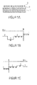
- Fig. 1A shows a schematic diagram of an information storage in a simple form, which works according to the mechanism of action.
- the information memory comprises an electrode 1, a charge carrier-conducting layer 2, and a nanoparticle layer 3.
- the electrode 1 provides charge carriers (electrons or holes).
- the charge carriers are conducted by means of the charge carrier-conducting layer 2 to nanoparticles, which are contained in the nanoparticle layer 3.
- the charge carrier-conducting layer may be a predominantly hole-conducting material or a predominantly electron-conducting material. The charge carriers remain in the nanoparticles when it is the most energetically favorable state for the nanoparticles.
- Fig. 1B is shown a simplified energy level scheme with electrons as charge carriers.
- the energy value W ⁇ vacuum level
- the energy level scheme Within the electrode 1, the energy level of the electrons is relatively high. In the charge carrier conductive layer 2, the energy level of the electrons is slightly lower. A local minimum of the energy level is achieved within the nanoparticles in the nanoparticle layer 3.
- Fig. 1B shows the energy level scheme, when the arrangement is subjected to an electrical voltage.
- the electrons initially accumulate at this electrode 1. If the electrode material now has a lower work function in comparison to the conduction band edge of the semiconductor nanoparticles, it is energetically more favorable for the negative charges (electrons), corresponding states in the Conduction band E c of the semiconductor nanoparticles to occupy. This process is in the in Fig. 1B illustrated basic energy level scheme shown. The electrons therefore flow via diffusion or tunneling processes in the direction of the semiconductor nanoparticles and are "stored" in them.
- these "delocalized” charges stored in the semiconductor nanoparticles cause the fluorescence property of the now ionized semiconductor nanoparticles to be affected, or "turn off,” thereby locally reducing the intensity (i.e., brightness) of the emitted fluorescence radiation.
- the original external electric field 7, which represents the information to be stored is optically detectable locally as a reduced fluorescence property of the nanoparticle arrangement.
- Fig. 1C indicates one Fig. 1 B equivalent energy level scheme, but with holes as charge carriers. Within the electrode 1, the energy level of the holes is shown relatively low. Note, however, that with holes the sign reverses, so that the actual energy of the holes within the electrode 1 is relatively high. In charge carrier-conducting material 2, the holes have a medium energy level and a local extreme value is achieved in the nanoparticles.
- Fig. 2A shows an expanded embodiment of the mechanism of action with electrons as to be stored in the nanoparticles charge carriers.
- the structure in this case comprises two parallel electrodes 1 and 5. Between the electrodes 1 and 5, a matrix material 2, 4 is arranged, which may consist of one or more functional layers, wherein at least a portion of the matrix material 2, 4 is to perform optically transparent , The electrons provided for storage in the nanoparticles are provided by the electrode 1 with a negative electrical potential. On the other electrode 5 are due to a positive electrical potential holes. The resulting electric field 7 allows a directed movement of the charge carriers.
- the appropriate choice of the matrix material 2 between negative electrode 1 and nanoparticle layer 3 allows the transport of electrons to the nanoparticles, while due to the insulating effect of the matrix material 4 between the positive electrode and nanoparticle layer, the holes are kept away from the nanoparticles.
- the matrix material 4 does not necessarily have to be an insulator.
- the nanoparticles in layer 3 can likewise be embedded in a matrix material 6. If this material is dimensioned such that it carries electrons, but keeps oppositely charged holes, the matrix material in layer 3 can also ensure selective charge carrier storage.
- Fig. 2B shows the energy level scheme to that in Fig. 2A illustrated schematic representation.
- the nanoparticles are embedded in a stabilizing, energetically adapted material 6.
- the electrons In order to emerge from the nanoparticle, the electrons must overcome an "energy gap" that has the height of the difference in energy levels between the interior of the nanoparticle 3 and the matrix 6.
- the visualized information is switched off again and the display is cleared by restoring the original fluorescence properties of the nanoparticles. This can be done for example by means of irradiation with intense, short-wave UV light or by applying a strong electric field.
- Fig. 3A shows a complementary schematic representation in comparison to in Fig. 2A illustrated schematic representation.
- holes serve as charge carriers to be stored in the nanoparticles.
- the electric Voltage poled so that it is a storage of holes and thus a suppression of photoluminescence.
- the matrix materials 2, 4 are to be chosen such that the transport of holes to the nanoparticles is ensured by the matrix material 2, 4, but the complementary electrons are kept away from the nanoparticles by the matrix material 2, 4.
- the information to be displayed can be erased by irradiating the nanoparticle layer with intense, short-wave UV light or by applying a strong electric field.
- Fig. 3B the energy level scheme is shown, which corresponds to the basic representation of Fig. 3A belongs.
- the holes first accumulate on the upper electrode 5, while the negative charges accumulate on the lower electrode 1.
- Has the electrode material as in Fig. 3B As shown, a lower work function compared to the valence band edge of the semiconductor nanoparticles, it is energetically favorable for the positive charges to occupy corresponding states in the valence band Ev of the semiconductor nanoparticles, as shown in principle in the energy level scheme of Fig. 3B is shown.
- the positive charges therefore flow via diffusion and tunneling processes in the direction of the semiconductor nanoparticles and are stored in these.
- the original, external electric field which represents the information to be stored, is optically detectable locally as a reduced fluorescence of the semiconductor nanoparticle arrangement of the information memory. Due to the storage effect of the nanoparticles, the information to be stored is also detectable for a period of time (up to several years) after the information has been written.
- the technical teaching presented herein makes it possible to use signs, displays and the like. with which information with the help of a one-time write process permanently stored and displayed with appropriate stimulation. For the further course no permanent electrical energy is needed anymore.
- the stored information can be visualized by a simple external optical excitation with a higher energy UV lamp.
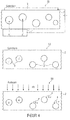
- Fig. 4 illustrates the operation principle of the disclosed information storage.
- Fig. 4 shows a nanoparticle arrangement 50 of a storage element of the information store in three different states, which may occur during use of the information store.
- the nanoparticle assembly comprises a plurality of nanoparticles or crystals 3 and a support material 2.
- the upper figure in Fig. 4 shows a writing state of the information memory.
- a first electrode 1 contacts a region of the support material 2, namely the left region. Another area (the right area) of the support material 2 is not directly contacted by the electrode 1.
- a second electrode 5 is arranged on the opposite side of the support material and contacts substantially the entire surface of the support material 2.
- an electrical voltage is applied, which causes electrons e - from the first electrode 1 through the Move support material 2 in the direction of the second electrode 5.
- the movement of the electrons essentially takes place in the region contacted by the first electrode 1 and its extension perpendicular to a surface of the support material 2 and is based essentially on tunneling and / or diffusion effects.
- Nanoparticles 3, which are in this region and its extension, have an increased probability of catching and absorbing carriers which are on the way from the first electrode 1 to the second electrode 5. These nanoparticles are subsequently electrically negatively charged.
- the further writing operation may be performed at a different timing than the first writing operation.
- the two writes may be temporally apart, e.g. a few hours, days, weeks, months or even years.
- a second region-selective electrical field is generated, with which the further information can be stored in the nanoparticle arrangement. This further writability can be used, for example, to record the state and / or history of an item or stored information and play it back when needed.
- the middle picture in Fig. 4 shows a memory state of the information memory. Apart from the usual environmental influences, no significant external energy acts on the nanoparticle arrangement 50.
- the negatively charged nanoparticles 3 are mainly located in an area defined by the electrode 1 during the writing process, and retain their negative electrical charge, ie, excess electrons e - , since electrons are the most energetically favorable location within the nanoparticles.
- the memory state can have a long life, which can be up to several years.
- the lower picture in Fig. 4 shows a readout state of the information memory.
- UV light ultraviolet light
- nanoparticles 3 are brought to light by means of photoluminescence, which do not contain any charge carriers, ie lie outside the range defined by the electrode 1 during the writing process. Within the range defined by the electrode 1, however, photoluminescence of the nanoparticles 3 is largely suppressed.
- the UV light can reach the nanoparticles and on the other hand a photoluminescence generated by the nanoparticles 3 without supplied charge carriers can pass through the support material 2, the support material 2 is at least partially transparent to the UV light used and that emitted by the nanoparticles photoluminescence. Since the region or the regions remain substantially dark during irradiation with the UV light, in which predominantly electrically charged nanoparticles are present, the information introduced into the nanoparticle arrangement 50 during the writing process can be made visible again.
- FIG. 12 is a schematic perspective view of an information store according to the disclosed teachings.
- the information storage essentially comprises the storage element, which in turn essentially comprises the nanoparticle arrangement 50.
- the nanoparticle assembly 50 which comprises the support material 2 and the nanoparticles 3.
- a region is shown that corresponds to the information to be stored (here, for example, the letter "A").
- Electrons e - are introduced as charge carriers over the surface of the nanoparticle assembly 50 within the region "A" into the nanoparticle assembly 50 and move substantially perpendicular to the surface through the nanoparticle assembly until they are (at least partially) supplied to the nanoparticles 3 present in this region ,
- semiconductor nanoparticles of different sizes have a different color of fluorescence emission, when a quantity of charge carriers Q 0 from the electrodes 1 and 5 respectively due to the different response differently sized semiconductor nanoparticles a corresponding color change in the fluorescence emission and thus obtain a color contrast become.
- the nanocrystals of different sizes can be present as a mixture in a single layer. Or the crystals of different sizes are spatially separated in several layers or areas.
- the nanoparticle assembly comprises a first layer in which primarily nanoparticles of a first size are present.
- the nanoparticle arrangement comprises a second layer, in which mainly second-sized nanoparticles are present, and comprises a third layer in which nanoparticles of a third order of magnitude are present.
- the nanoparticles of the first layer are smaller than the nanoparticles of the second layer, and the particles of the third layer each have a different size than the nanoparticles of the first and second layers.
- Devices for writing an information memory may further comprise, in addition to electrodes for storage, also erase electrodes.
- the erase electrodes can be formed flat.
- at least one of the erase electrodes may also be of rod-shaped design, so that the erase rod-shaped electrode is moved over the information memory to generate a erasing electric field therein, erasing all areas of the nanoparticle array of the information memory.
- the already mostly flat electrode 5 can be used as one of the erase electrodes.
- reading out the memory element of the information memory does not constitute a "reset” process with respect to the charge carriers stored in the semiconductor nanoparticle arrangement, since the charge carriers remain in the semiconductor nanoparticle arrangement even after reading the memory element (at least for the most part) stay saved.
- the information memory can be reset, for example, by applying a correspondingly aligned and sufficiently strong electric field to the semiconductor nanoparticle arrangement in order to "pull out” or remove the charge carriers stored in the semiconductor nanoparticles from the semiconductor nanoparticle arrangement.
- a reset process may be designed to supply charge carriers having an opposite polarity to the charge carriers of the semiconductor nanoparticle arrangement stored in the semiconductor nanoparticles in order to recombine the stored charge carriers with the supplied charge carriers and thus to "erase” the stored charge carriers make. This way you can the information store, for example, be brought back to a predefined initial state.
- the technical teaching disclosed herein is applicable in passive writable and optionally erasable or non-erasable displays.
- the teaching can be used as an electro-optical transducer (sensor), for protection against plagiarism or for event and condition monitoring, without the information being visible to anyone without assistance.
- Another field of application is as a guarantee label or generally for labeling.
- a passive display or permanently writable photoluminescent quantum dot display as disclosed herein may find application in a variety of fields, such as signage, stickers, labels, chalkboards, loose sheets, notebooks, books, and a flip chart.
- the information storage may comprise at least one of the electrodes 1 and / or 5. It is also possible that the information storage comprises a light source for optical excitation, so that the stored information is visible by activating the light source.
- the sensor arrangement 110 constructed, for example, as a layer stack has a force-sensitive element 120 and a display element 140 connected thereto.
- this vertical structure is only an example, wherein a laterally aligned arrangement of the force-sensitive element 120 and the display element 140 is conceivable.
- the force-sensitive element 120 and the display element 140 can thus be arranged one above the other or else next to one another with respect to the surface of the mechanical component 160.
- the sensor arrangement 110 is now, for example, directly attached to a mechanical component 160 to be monitored, ie the sensor arrangement 110 can be laminated on or into the mechanical component 160 (in the case of composite materials), for example, or can be injected into the mechanical component during injection molding in the case of injection-molded parts 160 be embedded.
- the sensor arrangement 110 can be laminated on or into the mechanical component 160 (in the case of composite materials), for example, or can be injected into the mechanical component during injection molding in the case of injection-molded parts 160 be embedded.
- Piezo elements in the form of piezoelectric ceramic materials, polymer films or ceramic-polymer composites may be used as the force-sensitive element 120, wherein at least one contactable electrode 124 is applied to a piezoelectric layer 122 of the force-sensitive element 120, where it is based on a mechanical load of the mechanical Component 160, that is, due to an external force, to provide an electric charge amount Q 0 of a charge carrier type.
- a further contactable electrode 126 can be provided, at which a corresponding charge quantity of the charge carrier type (complementary to the electrode 124) can be tapped off. If, therefore, the two electrodes 124, 126 are provided on the force-sensitive element 120, charge quantities Q 0 of a complementary charge carrier type are respectively provided there.
- the footprint of the force sensitive element 120 may be selected depending on the geometry of the mechanical component 160. Possible thicknesses of, for example, a piezoelectric element as the force sensitive element 120 can range from molecular monolayers to a few centimeters.
- any sensor elements which fall under the generic term “piezoelectric elements” and which provide a tapped voltage or charge quantity as output signal based on an acting mechanical load can thus be used as force-sensitive elements 120.
- the force-sensitive element 120 is now connected to the mechanical component 160 to be monitored in such a way (positive, positive or materially locking) in order to overcome the mechanical loads and forces acting on the mechanical component 160, for example as deformations of the mechanical component 160 and thus of the mechanical component 160 Force sensitive element 120 occur to record directly at the point of origin of the mechanical component 160.
- the force-sensitive element 120 is thus designed as a so-called force sensor or force sensor, with which a force is measured, which acts on the force-sensitive element 120, these being both compressive, tensile, shock and bending loads.
- the mechanical load (s) can be both static and dynamic.
- the z. B. is in the form of a piezoelectric layer, an electrical voltage across the force-sensitive element 120, which can be tapped off as a defined, electrical charge quantity Q 0 (of a charge carrier polarity) at the contact region 124.
- the force-sensitive element 120 can thus be designed to provide the amount of electrical charge Q 0 based on the applied mechanical load only when a limit value for the mechanical load is exceeded.
- the force-sensitive element 120 may be configured to continuously measure the amount of electric charge Q 0 based on and, for example, B. to provide proportional to the applied mechanical stress.
- the charge quantity Q 0 provided by the force-sensitive element 120 can now indicate on the one hand that a limit value for the mechanical load-bearing capacity of the mechanical component has already been exceeded.
- the amount of charge Q 0 provided by the force sensitive element 120 may be continuous and z. B. be generated in proportion to the applied mechanical stress, for example, over a predetermined period of time to reflect the total exerted on the mechanical component mechanical stress.
- the force-sensitive element 120 for providing an electrical charge quantity Q 0 which is based on the mechanical load acting on the coupled mechanical component 160, is now assigned a display element 140 with a semiconductor nanocrystal arrangement 142, wherein the semiconductor nanocrystal arrangement 142 has a fluorescence property, the amount of electric charge (one polarity) supplied based on one of the semiconductor nanocrystal arrangement can be set or changed.
- the force-sensitive element 120 is thus coupled to the display element 140, ie, for example, with a planar or structured electrode 144 of the display element 140 in order to supply at least a portion of the charge quantity Q 0 generated by the force-sensitive element 120 to the semiconductor nanocrystal arrangement of the display element 140.
- the display element 140 serves as a storage or indicator layer for the load state of the mechanical component 160.
- the semiconductor nanocrystal arrangement 140 has a large number of semiconductor nanocrystals or semiconductor nanoparticles 142-2 within a carrier material 142-1.
- a transparent one for the emitted fluorescence radiation Protective layer or a transparent and conductive counter electrode layer 148 may be arranged on the semiconductor nanocrystal arrangement 142.
- the electrode 144 assigned to the semiconductor nanocrystal arrangement 142 of the display element 140 is now accessible, for example, via one or more contacting intermediate layers 146, which are e.g. B. is permeable to each of the nanoparticles 142-2 to be supplied charge carrier type and impermeable to the complementary charge carrier / is connected to the contact region 124 of the force-sensitive element 120.
- the display element 140 is applied as a so-called semiconductor nanocrystal composite layer via the contacting (intermediate) layer (s) 146 to the force-sensitive element 120 formed as a piezoelement 122, whereby the in Fig. 6 shown layer stack for the sensor assembly 110 results.
- Example, in the form of lines, vias, etc, between one of the contact areas 124, 126 and one of the electrodes 144, 148 may be provided to supply the amount of electrical charge Q 0 of the desired charge carrier type nanoparticles 142-2.
- the contact region 124 and the electrode 144 may, for example, also be formed as a common element.
- the base area of the display element 140 of the sensor arrangement 110 there are no dimensional restrictions.
- the base area of the display element 140 can be selected depending on the geometry of the mechanical component 160. Possible thicknesses of the display element 140 can range from molecular monolayers to a few millimeters.
- semiconductor nanocrystals can be used with a higher energy optical excitation.
- B. by means of an external excitation device 180 in the form of a UV light source or a laser, etc. according to their band gap fluorescence radiation S fluorescence emit.
- the excitation of the semiconductor nanocrystals 142-2 in the semiconductor nanocrystal array 142 produces so-called electron-hole pairs (excitons) in the nanocrystals which recombine with the emission of a fluorescence photon.
- the respective wavelength (ie color) of the fluorescence emission of the display element 140 can be changed [3, 4].
- Semiconductor nanocrystals now have the property that the energy of the emitted fluorescence photons, ie the energy gap from the ground state to the excited state, not only of the respective semiconductor material the semiconductor nanocrystal, but also on the respective particle size of the semiconductor nanocrystals depends.
- differently sized particles 142-2 can be produced from the same semiconductor material, which fluoresce in different colors, wherein the color, ie the emission wavelength, can be set by the respective nanoparticle size.
- small particles emit at a smaller wavelength, ie at a larger photon energy, while larger particles emit at longer wavelengths, ie at smaller photon energies (see also quantum confinement effect). Due to the quantum mechanics, it can now be explained that the distance between the energy levels depends on the spatial dimensions, ie the particle size, due to the spatial limitation of the charge carriers.
- quantum dots quantum dots
- semiconductor materials for nanocrystals or nanoparticles can be used which, depending on their size and material, are in a wavelength range of, for example, 10 nm. B. from 400 nm to 1700 nm emit light, with the human visible spectral range of about 380 to 780 nm.
- core-type and core-shell nanocrystals of the semiconductor materials CdSe, CdTe, CdS, GaAs, GaSb, HgTe, InAs, InP, InSb, PbSe, PbS, PbTe, ZnSe, ZnTe, germanium and silicon.
- the fluorescence properties of the semiconductor nanocrystals i. H.
- the intensity and spectral position or width of the emission bands now depends in particular on electric fields and charges in the respective nanoparticles or in their surroundings.
- This property of semiconductor nanoparticles is now used in the sensor arrangement according to the invention to indicate the mechanical load of the mechanical component 160 detected by the force-sensitive element 120 by means of the display element 140 or its semiconductor nanocrystal arrangement 142.
- a quantum dot is a nanoscopic material structure that includes semiconductor material in the form of semiconductor nanoparticles in embodiments of the present invention.
- the charge carriers (electrons or holes) in a quantum dot are so limited in their mobility in all three spatial directions that their energy can no longer assume continuous values but only discrete values.
- the atomic order of quantum dots is about 10 2 -10 5 atoms.
- the semiconductor nanoparticles 142-2 are in one Carrier material 142-1 accommodated or embedded.
- the quantum dots ie, the semiconductor nanoparticles 142-2
- the quantum dots may be provided with a sheath layer or a wetting layer, wherein this sheath or wetting layer of the semiconductor nanoparticles may be formed so selectively during their production that the semiconductor nanoparticles different size responsive to a charge carrier supply from the electrode layer 144, that is, change the fluorescence properties of different sized semiconductor nanoparticles based on the introduced from the piezoelectric element 120 charge carriers differently.
- semiconductor nanoparticles of different sizes have a different color fluorescence emission
- the sensor effect of the sensor arrangement 110 according to the invention consists in the fact that the charges or charge carriers (of a charge carrier type) generated by the force-sensitive element 120 in the piezo layer 122 are transported to the respective semiconductor nanocrystals 142-2 and injected into the semiconductor nanocrystals.
- the nanoparticles are therefore ionized.
- electrons or holes are suitable, wherein the positively ionized state of nanoparticles is more stable in time due to the higher effective mass of the holes, and thus an information of each detected mechanical load condition of the monitored mechanical component 160 longer, z. B. up to several years, can be stored.
- a delocalization is a condition when a charge in an atomic group is not exactly localizable, but is distributed over the individual atoms.
- Auger recombination is now utilized in the sensor arrangement according to the invention in order to store or visualize the load state of the mechanical component 160 detected by the force-sensitive element 120.
- the charge quantity Q 0 generated by the force-sensitive element 120 will at least partially penetrate into the semiconductor nanocrystal arrangement via the electrode 144 of the display element 140 142, so that the fluorescence behavior of the semiconductor nanocrystal array 142 of the display element 140 (which is also called the indicator layer) changes due to the above-described physical relationships regarding the influence of the fluorescence property of the semiconductor nanocrystal array 142 based on the introduced charge amount Q 0 ,
- the fluorescence of the semiconductor nanocrystal arrangement 142 of the display element 140 will correspondingly change over the entire area or be reduced in the case of an optical excitation.
- the semiconductor nanocrystal arrangement 142 essentially has semiconductor nanoparticles 142-2 of the same type or size, the fluorescence property of the semiconductor nanocrystal arrangement 142 will be reduced over the entire area due to the charge carriers introduced. If the semiconductor nanocrystal assembly 142 z. For example, if different semiconductor nanocrystal particles 142-2 have either different materials or different sizes, the color composition of the fluorescent light emitted by the semiconductor nanocrystal array 142 will change, for example due to the different responses of the different groups of semiconductor nanoparticles as a color change of the fluorescent light is perceptible.
- predetermined regions of the semiconductor nanocrystal assembly 142 may include only one predetermined type of semiconductor nanoparticles 142-2, while other regions may comprise at least two or more different types of semiconductor nanoparticles.
- a perceptible contrast or a change in the representation can be clarified or reinforced on the basis of a mechanical load acting on the mechanical component 160.
- the electrode 144 of the display element 140 is metallized in regions, locally varying fluorescence reductions (corresponding to the structure of the electrode 144) in the semiconductor nanocrystal arrangement 142 can be produced, so that a measure of the mechanical stress on the mechanical component 160 is an optical contrast the emitted fluorescent light (eg, to adjacent sensor arrangements 110) becomes visible directly on the mechanical component to be monitored.
- the metallization of the electrode 144 may be configured to be associated with a particular type of semiconductor nanoparticle (if multiple types of semiconductor nanoparticles are provided) in the semiconductor nanocrystal assembly 142.
- the semiconductor nanoparticles which are assigned to the electrode areas 144 or are arranged adjacent to them thus, preferably receive the charge carriers which change the fluorescence behavior.
- the semiconductor nanocrystal arrangement 142 is significantly increased due to increased contrasts between a "normal" fluorescence property and a "changed” fluorescence property.
- intermediate stages corresponding to the respectively supplied, z. B. different charge amount Qo are clearly displayed, so that corresponding intermediate stages of the mechanical component 160 acting on mechanical stress can be reproduced.
- this contrast i. H. the change of the fluorescence property of the sensor arrangement 110 according to the invention, for example with the human eye, if the emitted fluorescent light lies in the visible range, or be registered by means of corresponding detection devices or cameras.
- the mechanical stress state of the mechanical component 160 to be monitored depends relatively largely on the immediate surroundings of the semiconductor nanocrystals, ie essentially on the material layer 142-1 surrounding the semiconductor nanoparticles and / or on the optional additional embedding material in which the quantum dots are embedded can.
- the layered material 142-1 of the semiconductor nanocrystal assembly may be present as a composite of two or more bonded materials.
- particles or fibers are embedded in another component of the composite, the so-called matrix.
- matrix materials the electrical materials, such as polymer, ceramic or glass materials, conductive and semiconducting organic substances, such as various thiophenes, BCP, TPD, CBP, or composites with conductive particles and fibers, for Example, TiO 2 , ZnO, ITO, silver, gold, graphite, graphite fibers, CNT, can be used. This list is to be regarded as exemplary and not as exhaustive.
- Fig. 7A 1 shows a possible exemplary embodiment of the sensor arrangement 110 according to the invention in the form of a functional double layer of the sensor arrangement 110 arranged as a layer stack with the force-sensitive element 120 and the display element 140 Fig. 7A is shown, the force-sensitive element 120, for example in the form of a piezoelectric element, positively, positively or materially connected to the mechanical component 160 to be monitored or embedded in the same.
- the piezoelement 120 is now, for example, polarized in such a way that the negative charges Q 0 (electrons) accumulate on the upper electrode 124 when force is applied, while the positive charges accumulate on the optional further electrode 126.
- this piezoelement 120 is connected to the semiconductor nanocrystal arrangement 140 arranged above or to an electrode (not shown in FIG. 1) associated with the semiconductor nanocrystal arrangement 142 Fig. 7A ) conductively connected.
- the carrier material 142-1 of the semiconductor nanocrystal arrangement 142 in which the semiconductor nanocrystals or semiconductor nanoparticles are embedded, may for example consist of a few nanometers (eg 10-100 nm) to several millimeters (eg. 1-10mm) thick electrical polymer layer.
- the semiconductor nanocrystals 142-2 are embedded, for example, in a carrier material 142-1 of the semiconductor nanocrystal arrangement 142 designed as an electron-conducting matrix material.
- in Fig. 7A represented electrode 124, the same time the function of in Fig. 6 represented electrode 144, over the entire surface, ie metallized throughout, or even structured, ie, metallized area, be formed.
- Fig. 7B now shows in a simplified view a principle energy level scheme for the in Fig. 7A
- the mechanical component 160 is deformed due to an external mechanical load or force
- charges are generated in the force-sensitive element 120, which is frictionally coupled to the mechanical component 160 (in the piezoelectric layer)
- the resulting charge quantity Q 0 is dependent on the strength of the applied mechanical load, ie occurs when a mechanical limit is exceeded or the mechanical load is proportional.
- the electrons accumulate first at the (upper) electrode 124.
- the electrode material as here in Fig.
- FIG. 7B shown a lower work function compared to the conduction band edge of the semiconductor nanocrystals 142-2, it is energetically more favorable for the negative charges (electrons) to occupy corresponding states in the conduction band E c of the semiconductor nanocrystals 142-2.
- This process is in the in Fig. 7B illustrated basic energy level scheme by means of the arrow between the areas 124 and 142-2. The electrons therefore flow via diffusion or tunneling processes in the direction of the semiconductor nanocrystals 142-2 and are "stored" in them.
- these "delocalized” charges stored in the semiconductor nanocrystals 142-2 cause the fluorescence property of the now ionized semiconductor nanocrystals to be "turned off” and thus a local reduction in intensity (ie, brightness) of the emitted fluorescence radiation.
- the original, external force acting on the mechanical component 160 to be monitored is visually detectable locally as a reduced fluorescence property of the display element 140.
- the detectability of a change in the fluorescence property of the display element 140 can be further enhanced by structuring the electrode structure 144, for example in a linear grid, so that, corresponding to the ionization of the semiconductor nanocrystals in the vicinity of the metallic regions of the electrode 144 associated fluorescence property of the semiconductor nanocrystals changes, so that, for example, results in a line contrast, which is the higher, the greater the amount of charge provided by the force-sensitive element 120 Q 0 .
- different types of semiconductor nanoparticles of different size and / or material composition may also be combined in the semiconductor nanocrystal assembly 140.
- the mechanical action of an external force on the mechanical component 160 to be monitored is also for a period of time, for example at least hours or even days and up to several years after the event, ie. H. the mechanical load, detectable.
- FIGS. 8A-B a further basic embodiment of the sensor arrangement 110 according to the invention and explained their basic operation.
- the force-sensitive element 120 for example in the form of a piezoelectric element, is in turn attached non-positively to the mechanical component 160.
- the piezoelectric layer 120 is polarized in such a way that whose upper electrode 126 collect the negative charges, while at the lower electrode 124, the positive charge carriers (charge amount Q 0 ) accumulate.
- the semiconductor nanocrystals 142 - 2 are embedded in a carrier material 142 - 1 of the semiconductor nanocrystal arrangement 142 designed as a hole-conducting matrix material.
- an insulating layer 146 is inserted as an electron block layer.
- a transparent counter electrode 144 is electrically connected to the lower electrode 124 of the piezoelectric layer 120.
- the mechanical stress acting on the mechanical component 160 to be monitored is made visible by means of the semiconductor nanocrystal arrangement 142 arranged in the display element 140 by, for example, stimulating fluorescence of the semiconductor nanocrystal arrangement 142 by means of an external optical excitation the component loading results as an optical contrast in the fluorescence emission.
- the electrons first collect again at the upper electrode 124, while the positive charges accumulate at the lower electrode 126, which accumulates with the electrode layer 144 of the display element 140 connected is.
- Has the electrode material as in Fig. 8B As shown, having a lower work function compared to the valence band edge of the semiconductor nanocrystals, it is energetically more favorable for the positive charges to occupy corresponding states in the valence band Ev of the semiconductor nanocrystals 142-2, as shown in principle in the energy level scheme of Fig. 8B is shown.
- the positive charges therefore flow through diffusion and tunneling processes in the direction of the semiconductor nanocrystals 142-2 and are stored in these.
- these charges cause the fluorescence property of the ionized semiconductor nanocrystals 142-2 to be changed.
- the original, external force on the device 160 is optically detectable locally as a reduced fluorescence of the semiconductor nanocrystal array 142 of the display element 140. Due to the storage effect of the nanocrystals, the effect of the external force on the mechanical component 160 to be monitored is also detectable for a period of time (up to several years) after the event of the mechanical load being applied.
- the force-sensitive element 120 (in the form of a piezoelectric element) is positively, positively or materially attached to the mechanical component 160 to be monitored or embedded therein.
- the piezoelectric layer 122 of the force-sensitive element 120 is now, for example, polarized such that the positive charge carriers accumulate on the upper electrode 124, while the negative charge carriers (electrons) accumulate on the lower electrode 126.
- the semiconductor nanocrystals 142-2 are now embedded in an electron-conducting matrix 142-1.
- a positive-carrier insulating layer 146 is interposed between the upper electrode 126 of the force-sensitive element 120 and the semiconductor nanocrystal assembly 142, ie, the corresponding nanocrystal composite layer 142.
- a transparent counterelectrode 148 which has a full area or structured design, is arranged, for example, on the main surface of the semiconductor nanocrystal arrangement 142 remote from the force-sensitive element 120 and closes the layer structure of the sensor arrangement 110 upwards.
- the electrode structure 144 of the display element 140 is electrically connected to the electrode 126 of the force-sensitive element 120.
- the electrons generated by a force acting on the mechanical component 160 to be examined in the force-sensitive element 120 flow via the transparent cover electrode 148 and the carrier material 142-1 of the semiconductor nanocrystal assembly 142 to the insulating layer 146. At least a portion of the electrons thereby becomes semiconductor Nanoparticles 142-2 injected and stored, which in turn gives the fluorescence property the display element 140 is influenced or at least partially suppressed.
- the mechanical load acting on the mechanical component 160 is hereby also visually rendered visible.
- FIG. 9B In turn, in principle, the energy level scheme with the relevant energy levels for the basis of Fig. 9A shown embodiment inventive sensor assembly 110 shown.
- the positive charges accumulate on the upper electrode 124, while the negative charges accumulate on the lower electrode 126 connected to the electrode layer 144 of the display element 140.
- a lower work function compared to the conduction band edge of the semiconductor nanocrystals 142-2, it is energetically favorable for the negative charges to occupy corresponding states in the conduction band E C of the semiconductor nanocrystals 142-2, as in principle in the energy level scheme of Fig. 9B is shown.
- the negative charges therefore flow through diffusion and tunneling processes in the direction of the semiconductor nanocrystals 142-2 and are stored in these.
- these charges cause the fluorescence property of the ionized semiconductor nanocrystals 142-2 to be changed.
- the original, external force is locally optically detectable as a reduced fluorescence of the semiconductor nanocrystal array 142 of the display element 140. Due to the storage effect of the nanocrystals, the effect of the external force on the mechanical component 160 to be monitored is also detectable for a period of time (up to several years) after the event of the mechanical load being applied.
- any mixed colors for the fluorescence emission can also be set.
- the semiconductor nanoparticles 142-2 or crystals may be arranged in the matrix material 142-1 corresponding to the metallized regions of the patterned electrode 144.
- the color component of this type of semiconductor nanocrystals can be achieved from the fluorescence emission and thus result in a corresponding color transition. This color transition is even stronger, d. H. higher contrast, the more charge carriers are injected into the corresponding regions of the matrix material 142-1 from the contact electrode 144.
- the contact electrode 144 formed over the entire surface or in a correspondingly fine grid, a full-surface, continuous color transition can be achieved in accordance with the mechanical stress acting on the mechanical component 160 to be monitored. Furthermore, it is possible, according to the structuring of the contact electrode 144, to provide any predefined symbols, characters or character structures in the semiconductor nanocrystal arrangement 142 of the display element 140 which increasingly emerge based on the detected mechanical load or exceed a maximum allowable load Boundary load emerge.
- the resulting fluorescence properties can be adjusted in a targeted manner.
- a full-area "continuous" color transition of the display element 140 can be achieved, for example, in which the contact electrode 144 is arranged in a sufficiently fine (no longer resolvable by the human eye) grid, wherein the semiconductor nanoparticles of one of the plurality of different types of semiconductor nanocrystals with corresponding to a different fluorescence property, ie, following the grid, is arranged in the matrix material 142-1.
- FIG. 10 A method for displaying or storing and storing a mechanical load applied to a mechanical component 160 is shown.
- an electrical charge quantity is initially generated in a first step 1102 by means of a force-sensitive element that is positively, positively or materially connected to the mechanical component, wherein the electrical charge quantity Q 0 is based on a mechanical load acting on the mechanical component based.
- a step 1104 at least a part of the amount of electric charge Q 0 generated by the force sensitive element is supplied to a semiconductor nanocrystal of a display element, the semiconductor nanocrystal having a fluorescence characteristic changing based on the amount of electric charge supplied.
- the fluorescence property of the semiconductor nanocrystal arrangement of the display element is activated, for example, with a higher-energy, optical excitation, wherein the excited fluorescence property is based on the mechanical load acting on the mechanical component due to the amount of electrical charge Q 0 applied by the force-sensitive element.
- the force-sensitive element 120 for example in the form of a piezoelectric element, is positively, positively or materially connected to the mechanical component 160 to be treated or embedded in the same.
- the force-sensitive element is laminated to / in the material of the mechanical component 160 or embedded in the material of the mechanical component.
- the semiconductor nanocrystal arrangement of the display element is then excited to emit fluorescent light by means of a high-energy optical excitation, for example by means of a UV light source or a laser, etc.
- the emitted fluorescent light can be exposed to the mechanical stress acting on the mechanical component or up to now the mechanical component be assigned to mechanical stress.
- a changing or adjustable fluorescence property of a semiconductor nanocrystal arrangement 142 is used for a display element 140 to provide a measure of a mechanical load applied to a mechanical component 160 by a force-sensitive element 120, at least until "read-out” by means of an excited fluorescence emission , save.
- the fluorescence property of the semiconductor nanocrystal arrangement varies with the amount of electric charge coming from a is provided with the monitored mechanical component coupled force sensitive element.
- a readout of the display element 140 of the sensor arrangement 110 does not represent a "reset process" with respect to the charge carriers stored in the semiconductor nanocrystal arrangement 142, since the charge carriers continue to be present (at least for the most part) after a readout of the display element 140. remain stored in the semiconductor nanocrystal array 142.
- a reset of the sensor arrangement 110 according to the invention can be effected, for example, by applying a suitably aligned and sufficiently strong electric field to the semiconductor nanocrystal arrangement 142 of the display element 140, around the charge carriers from the semiconductor nanocrystal arrangement 142 stored in the semiconductor nanoparticles 142-2 "remove” or remove.
- a reset operation may be configured to supply charge carriers of opposite polarity to the charge carriers stored in the semiconductor nanoparticles 142-2 of the semiconductor nanocrystal device 140 to recombine the stored charge carriers with the charged carriers, thereby "quenching" "make the stored charge carrier.
- the sensor arrangement 110 according to the invention can, for example, be restored to a predefined initial state.
- the sensor arrangement formed as a sensor layer stack can be composed individually and application-specifically by means of the force-sensitive element and the display element with the semiconductor nanocrystal arrangement, depending on the size of the component and the target load or total load to which the mechanical component can be loaded.
- the amount of charge generated on the mechanical component as a function of the mechanical load is defined by the force-sensitive element.
- the amount of electric charge provided by the force-sensitive element is very precisely definable with respect to a mechanical load acting on the mechanical component.
- the use of semiconductor nanocrystals of different sizes can in principle realize different-colored display modes, for which purpose the electrode adjacent to the matrix material of the semiconductor nanocrystal arrangement and / or the semiconductor nanoparticles embedded in the matrix material are designed and arranged accordingly.
- the sensor arrangement formed as a sensor layer structure is also a variety of different materials, d. H. Polymer materials, conductor and semiconductor nanocrystals, available to selectively adjust the particular desired dependence of the excited fluorescence emission of the applied mechanical stress on the mechanical component can.
- the procedure according to the invention enables direct material-integrated detection, storage and evaluation or visualization of load conditions on mechanical components.
- the procedure according to the invention also makes it possible to correlate a defined mechanical load in the form of tension, pressure, impact, bending, etc. directly with an optical contrast in the fluorescence emission of the display element.
- no detour over electrical measurements is necessary, whereby the component integration and handling of the sensor arrangement according to the invention on or in a mechanical component to be examined is greatly simplified.
- the sensor arrangement according to the invention no structural change of the expected mechanical components is required.
- the sensor arrangements designed as indicator layers can be applied to the entire component surface or to predestined, safety-relevant points. A constructive intervention in the structure of the mechanical components used so far is not required.
- the present inventive concept serves the material-integrated detection, storage and evaluation of load conditions on mechanical components.
- the focus of the application can be placed on modern composite materials, but the inventive concept is by no means limited thereto.
- the procedure according to the invention is also suitable for use on conventional materials, such as, for example, metals, metal alloys, plastics, etc. Since mechanical components are used universally in all areas of technology, the concept according to the invention can be applied in a very versatile manner. By way of example, components for vehicle construction, aircraft construction, wind turbines, etc. are to be mentioned here.
- an information storage device comprises a storage element with a nanoparticle arrangement 50 which comprises a multiplicity of nanoparticles 3 and a support material 2 surrounding the nanoparticles; wherein the memory element is designed, in a first operating state, to supply electrical charge carriers e 1, p selectively to the nanoparticles 3 in a specific manner, and to substantially prevent a run - off of the supplied charge carriers from the nanoparticles 3 in a second operating state, wherein the supplied charge carriers e - , p change a fluorescence property of the nanoparticles 3 to which the electrical charge carriers in the first operating state have been selectively supplied selectively, so that it can be determined by optical excitation of the memory element, where the electrical charge carriers were partially selectively supplied to the nanoparticles 3 during the first operating state.
- an energy band profile through the nanoparticle arrangement 50 has local minima with respect to the charge carriers within the nanoparticles 3, so that in the second operating state at least part of the supplied charge carriers remain in the nanoparticles 50 as long as one of them is supplied Charge carriers added amount of energy is not sufficient to overcome an energy surrounding the local minimum, wherein in a nanoparticle 3 supplied charge carriers reduce a radiative recombination within the nanoparticle and thereby change the fluorescence properties of the nanoparticle, so that a presence of supplied charge carriers in the nanoparticles 3 through detect a degree of photoluminescence based on radiative recombination at the optical excitation of nanoparticle 3.
- the support material 2 is a predominantly hole-conducting material or a predominantly electron-conducting material or an insulating material.
- the information storage nanoparticles 3 have a band gap having a width between 0.7 eV and 3.0 eV.
- the memory element of the information memory is designed, in the first operating state when applying an electric field, to cause the electrical charge carriers to be selectively supplied to the nanoparticles 3 in certain regions.
- the storage element of the information memory is adapted to adopt, in addition to the first operating state and the second operating state, a third operating state in which the memory element is adapted to be extinguished by applying a clearing electric field or by irradiation with intense, short-wave UV light and the resulting discharge of the charged charge carriers from the nanoparticles 3.
- the information storage support material 2 comprises a material selected from: dielectrics such as PMMA, PS, PC, PVDF, PA, PP, PE, PVC, thermoplastics (PET , Polyether ketones), thermosets (polyesters, formaldehyde resins, epoxy resins, polyurethanes); conductive materials, such as polyelectrolytes, PEDOT, BCP, TPD, PPy, TCNQ complexes, PANI, PVK, tetracene, pentacene, phthalocyanines, polythiophenes, PTCDA, MePTCDI, quinacridone, acridone, indanthrone, flavanthrone, perinone, Alq3, P3HT, CNTs, wherein the support material 2 comprises the selected material in pure form, in doped form or as a derivative.
- dielectrics such as PMMA, PS, PC, PVDF, PA, PP, PE, PVC, thermoplastics (PET , Polyether ketones), thermo
- the nanoparticle assembly 50 of the information storage includes first, second and third layers, wherein in the first layer nanoparticles having a size in one In the second layer, nanoparticles having a size in a second size range predominate, and in the third layer, nanoparticles with a size in a third size range predominate.
- the information storage device further comprises an electrode arrangement 1, 5, which is designed to generate an electric field in the nanoparticle arrangement 50 in the first operating state, so that charge carriers are guided to the nanoparticles and at least a part thereof remain as charged charge carriers in the nanoparticles 3 as the charged carriers.
- the optical information carrier comprises an information storage having the above-mentioned features.
- the optical information carrier further comprises a light source for optically exciting the storage element of the information storage.
- a twelfth aspect relates to the use of an information memory according to any one of the first to ninth aspects of a passive display.
- an information storage apparatus comprises a receptacle 87 adapted to receive the information storage 9; and an electrode assembly 1, 5 comprising at least one patterned electrode 1 adapted to come into contact with the information memory 9 when the information memory is present in the receptacle 87, and to selectively generate an electric field in the information memory 9 in regions.
- the electrode assembly comprises an erase electrode configured to expose the information memory 9 to a stronger electric field than the electric field used to store the information, the erase electrode extending at least in one Dimension extends such that a deletion of a substantially planar memory element can be done by applying or sweeping the memory element through the erase electrode, in which the nanoparticles previously supplied charge carriers are removed by a strong electric field from the nanoparticles substantially.
- the apparatus further comprises a radiation source for erasing the information memory configured to emit higher energy electromagnetic radiation toward the information storage whose energy is sufficient, the charge carriers previously supplied to the nanoparticles to remove the nanoparticles.
- a method of storing information comprises: providing a nanoparticle assembly 50 comprising a plurality of nanoparticles 3 and a support material 2 surrounding the nanoparticles; Generation of a partially selective electric field in the nanoparticle assembly 50, so that the nanoparticles 3, which are detected by the partially selective electric field, charge carriers are supplied; Termination of the generation of the partially selective electric field, wherein the nanoparticle assembly 50 substantially prevents the charge carriers from flowing out of the nanoparticles 3 after termination and wherein the charge carriers change a fluorescence property of the nanoparticles 3 to which the electrical charge carriers during the generation of the electric field In some areas selectively supplied, so that it can be determined by optical excitation of the nanoparticle assembly 50, where in the first operating state, the electrical charge carriers were partially selectively supplied to the nanoparticles 3.
- the method further comprises generating a quenching electric field or a quenching higher-energy electromagnetic radiation in the nanoparticle assembly 50 prior to the generation of the partially selective field.
- the method further comprises generating a second area selective electric field in the nanoparticle assembly 50, such that the Nanoparticles 3, which are detected by the second selective selective electric field, additional charge carriers are supplied, wherein the generation of the selectively selective electric field and the second region-wise selective electric field takes place at different times.
- a sensor arrangement 110 has the following features: a force-sensitive element 120 for providing an electrical charge quantity Q 0 based on a mechanical load acting on a coupled mechanical component 160; and a display element 140 having a semiconductor nanocrystal array 142 for providing a fluorescence property that is adjustable based on an amount of electrical charge applied to the semiconductor nanocrystal array 142, wherein the force sensitive element 120 is coupled to the display element 140 so as to correspond to the semiconductor nanocrystal array of FIG Display element to supply at least a portion of the amount of charge generated by the force-sensitive element to change the fluorescence property of the display element 140 based on the detected by the force-sensitive element mechanical load.
- the force sensitive element 120 comprises a piezoelectric element 122 having at least one contactable electrode 124, 126 to provide at least one electrode 124, 126 an amount of charge Q 0 dependent on an applied mechanical stress.
- the semiconductor nanocrystal structure of the display element 140 has semiconductor nanocrystals 142-2 embedded in a material layer 142-1, the display element 140 being connected to the electrode 124, 126 of the piezoelectric element 122.
- the dielectric material layer, a polymer layer or a 0 conductive material for the charge carrier type of the provided at the electrode 124, 126 of the piezoelectric element 122 to charge amount Q referring back to the twenty-first aspect 142-1, the dielectric material layer, a polymer layer or a 0 conductive material for the charge carrier type of the provided at the electrode 124, 126 of the piezoelectric element 122 to charge amount Q.
- the display element 140 has a flat or structured trained contact electrode 144, which is adjacent to a main surface of the material layer 142-1 with the nanocrystals 142-2 and further connected to the electrode 124, 126 of the piezoelectric element 122.
- an insulating layer is disposed on another main surface of the material layer 142-1.
- the semiconductor crystal nanostructure assembly 142 of the sensor assembly comprises at least two different types of semiconductor nanocrystals 142-1 having different fluorescence properties.
- the different types of semiconductor nanocrystals 142 - 2 are embedded differently distributed in the material layer 142 - 1, wherein the contact electrode 144 of the display element 140 is structured to be provided by the force-sensitive element 120 Charge amount Q 0 is at least partially supplied to the semiconductor nanocrystals 142-2 of a type.
- the material layer 142-1 has a thickness in a range of 1 nm to 10 millimeters, with the material layer 142-1 emitting for the semiconductor nanocrystals 142-2 Fluorescence radiation is transparent.
- the force-sensitive element 120 and the display element 140 of the sensor assembly are each layered and stacked as a stack of layers or juxtaposed as individual layers.
- the force-sensitive element 120 is the sensor assembly designed so as to provide the amount of electrical charge Q 0 based on the applied mechanical load only when exceeding a limit value for the mechanical stress.
- the force sensitive element 120 of the sensor array is configured to continuously provide the amount of electric charge Q 0 based on the applied mechanical load.
- a mechanical component 160 includes a sensor assembly 110 according to any one of the nineteenth to thirtieth aspects for monitoring and displaying a mechanical stress applied to the mechanical component.
- a method 1100 of displaying a mechanical stress applied to a mechanical component includes the steps of: generating 1102 an amount of electrical charge Q 0 with a force sensitive element 120 connected to the mechanical device based on a mechanical device acting mechanical stress; Supplying 1104 at least a portion of the amount of electric charge generated by the force-sensitive element to a semiconductor nanocrystal array of a display element, the semiconductor crystal array having a fluorescence characteristic changing based on the amount of electric charge supplied; and exciting 1106 the fluorescence property of the semiconductor nanocrystal array in the display element, the excited fluorescence emission due to the amount of electric charge supplied by the force sensitive element correlating with the mechanical stress applied to the mechanical component.
- the force-sensitive element is in this case connected to the mechanical component in a force, form or material fit.
- the force-sensitive element is attached to the material of the mechanical component laminated or embedded in the material of the mechanical component.
- the method further comprises a step of associating the excited fluorescent emission with a mechanical stress applied to the mechanical component.
- a thirty-sixth aspect relates to the use of a semiconductor nanocrystal assembly for storing and / or displaying a measure of a mechanical load sensed by a force sensitive element and applied to a mechanical component.
- a fluorescence property of the semiconductor nanocrystal device changes based on an electric charge amount provided by a force-sensitive element coupled to the mechanical device.
- the semiconductor nanocrystal assembly is part of the sensor arrangement according to any one of the nineteenth to thirtieth aspects.
- aspects have been described in the context of a device, it will be understood that these aspects also constitute a description of the corresponding method, so that a block or a component of a device is also to be understood as a corresponding method step or as a feature of a method step. Similarly, aspects described in connection with or as a method step also represent a description of a corresponding block or detail or feature of a corresponding device.
Landscapes
- Engineering & Computer Science (AREA)
- Chemical & Material Sciences (AREA)
- Nanotechnology (AREA)
- Physics & Mathematics (AREA)
- Theoretical Computer Science (AREA)
- Biophysics (AREA)
- Optics & Photonics (AREA)
- Life Sciences & Earth Sciences (AREA)
- Crystallography & Structural Chemistry (AREA)
- General Physics & Mathematics (AREA)
- Light Receiving Elements (AREA)
- Luminescent Compositions (AREA)
- Semiconductor Memories (AREA)
- Investigating, Analyzing Materials By Fluorescence Or Luminescence (AREA)
- Optical Recording Or Reproduction (AREA)
Abstract
Ein Informationsspeicher umfasst ein Speicherelement mit einer Nanopartikelanordnung (50), welche eine Vielzahl von Nanopartikeln (3) und ein die Nanopartikel umgebendes Stützmaterial (2) umfasst. Das Speicherelement ist ausgelegt, in einem ersten Betriebszustand elektrische Ladungsträger (e - , p) bereichsweise selektiv den Nanopartikeln (3) zuzuführen, und in einem zweiten Betriebszustand einen Abfluss der zugeführten Ladungsträger aus den Nanopartikeln im Wesentlichen zu verhindern. Die zugeführten Ladungsträger ändern eine Fluoreszenzeigenschaft der Nanopartikel, denen die elektrischen Ladungsträger in dem ersten Betriebszustand bereichsweise selektiv zugeführt wurden, so dass durch optische Anregung des Speicherelements feststellbar ist, wo während des ersten Betriebszustands die elektrischen Ladungsträger bereichsweise selektiv den Nanopartikeln zugeführt wurden. Weiterhin werden offenbart: Eine Vorrichtung und ein Verfahren zum Speichern von Informationen in einem solchen Informationsspeicher und ein optischer Informationsträger.An information storage comprises a storage element with a nanoparticle arrangement (50), which comprises a multiplicity of nanoparticles (3) and a support material (2) surrounding the nanoparticles. In a first operating state, the memory element is designed to selectively supply electrical charge carriers (e, p) to the nanoparticles (3) in regions, and to substantially prevent a discharge of the supplied charge carriers from the nanoparticles in a second operating state. The supplied charge carriers change a fluorescence property of the nanoparticles, to which the electrical charge carriers in the first operating state have been selectively supplied in regions, so that it can be determined by optical excitation of the storage element where, during the first operating state, the electrical charge carriers were selectively supplied to the nanoparticles. Further disclosed are: An apparatus and a method for storing information in such an information storage and an optical information carrier.
Description
Die vorliegende Erfindung bezieht sich auf Informationsspeicher, auf optische Informationsträger, auf eine Verwendung eines Informationsspeichers für ein passives Display, auf eine Vorrichtung zum Speichern von Informationen in einem Informationsspeicher und auf ein Verfahren zum Speichern von Informationen. Insbesondere bezieht sich die vorliegende Erfindung auf das Speichern von Informationen in einer Nanopartikelanordnung auf elektrischem Weg und auf ein Auslesen der gespeicherten Information auf optischem Weg zu einem späteren Zeitpunkt.The present invention relates to information storage devices, to optical information carriers, to a use of a passive display information storage device, to an information storage device for information storage, and to a method for storing information. In particular, the present invention relates to the storage of information in a nanoparticle assembly by electrical means and to a readout of the stored information optically at a later time.
Die vorliegende Erfindung bezieht sich ferner auf eine Sensoranordnung unter Verwendung des Informationsspeichers, auf ein mechanisches Bauteil mit integrierter Sensoranordnung zur Überwachung und Anzeige einer auf das mechanische Bauteil einwirkenden mechanischen Belastung, auf ein Verfahren zum Anzeigen und Speichern einer auf ein mechanisches Bauteil ausgeübten mechanischen Belastung, und auf die Verwendung einer Halbleiter-Nanokristallanordnung zur Visualisierung (Speicherung und/oder Anzeige) einer von einem kraftsensitiven Element erfassten, auf ein mechanisches Bauteil einwirkenden mechanischen Belastung. Insbesondere bezieht sich die vorliegende Erfindung auf Verfahren und Vorrichtungen zum Detektieren, Speichern und Auswerten von statischen oder dynamischen Belastungen an mechanischen Bauteilen unter Verwendung eines kraftsensitiven Elements und eines mit dem kraftsensitiven Element verbundenen Anzeigeelements, wobei das Anzeigeelement eine Halbleiter-Nanokristallanordnung zum Bereitstellen einer Fluoreszenzeigenschaft aufweist, die basierend auf einer elektrischen Ladungsmenge, die der Halbleiter-Nanokristallanordnung von dem kraftsensitiven Element zugeführt wird, änderbar bzw. einstellbar ist.The present invention further relates to a sensor arrangement using the information memory, to a mechanical component with integrated sensor arrangement for monitoring and displaying a mechanical load acting on the mechanical component, to a method for displaying and storing a mechanical load applied to a mechanical component, and to the use of a semiconductor nanocrystal arrangement for the visualization (storage and / or display) of a mechanical load detected by a force-sensitive element and acting on a mechanical component. In particular, the present invention relates to methods and apparatus for detecting, storing and evaluating static or dynamic loads on mechanical components using a force sensitive element and a display element connected to the force sensitive element, the display element comprising a semiconductor nanocrystal array for providing a fluorescence property which is changeable based on an amount of electric charge supplied to the semiconductor nanocrystal array from the force sensitive element.
In vielen Bereichen des täglichen Lebens werden Informationen verschiedenster Art verarbeitet und für einen reibungslosen Ablauf vieler Vorgänge sind Informationen erforderlich. Die Informationen werden einem Informationsempfänger auf unterschiedlichste Weise zur Verfügung gestellt. Dazu gehören u.a. akustische Signale aber auch optische Informationen.In many areas of daily life, information of various kinds is processed and information is required for the smooth running of many processes. The information is provided to an information recipient in a variety of ways. These include u.a. acoustic signals but also optical information.
Es gibt verschiedenste Möglichkeiten, Menschen optische Informationen zur Verfügung zu stellen. Im Wesentlichen lassen sich diese Möglichkeiten in zwei Gruppen unterteilen: Zum Einen Vorrichtungen, bei denen die Information während eines Herstellungsprozesses auf oder eingebracht werden, und zum Anderen Vorrichtungen, bei denen die Information während des Betriebs geändert werden kann.There are various ways to provide optical information to people. In essence, these possibilities can be divided into two groups: On the one hand, devices in which the information is placed on or during a manufacturing process, and on the other hand devices in which the information can be changed during operation.
Zu der ersten Gruppe gehören beispielsweise Schilder, Zeitungen, usw.. Im Allgemeinen wird die Information durch die gezielte Verteilung von Materialien wie Tinte, Farbe, Partikeln oder vieles andere auf der Vorrichtung relativ dauerhaft zur Verfügung gestellt. Ein Beispiel für eine derartige Vorrichtung ist in der internationalen Patentanmeldung mit der Veröffentlichungsnummer
Zu der zweiten Gruppe, also Vorrichtungen, bei denen die Information während des Betriebs geändert werden kann, gehören z.B. Fernsehgeräte, mobile Kommunikationsgeräte, Displays (beispielsweise bestehend aus Leuchtdioden (LEDs "light emitting diodes"), organischen Leuchtdioden (OLEDs "organic light emitting diodes") oder Flüssigkristallanzeigen (LCDs "liquid crystal displays"). Vorrichtungen der zweiten Gruppe benötigen zu ihrem Betrieb typischerweise permanent Energie.The second group, ie devices in which the information can be changed during operation, includes e.g. Television sets, mobile communication devices, displays (for example comprising light emitting diodes (LEDs), organic light emitting diodes (OLEDs) or liquid crystal displays (LCDs)) Devices of the second group require their operation typically permanent energy.
Als besondere Gruppe von Displays sei an dieser Stelle auf sogenannte Quantenpunktdisplays ("Quantum Dot Displays") verwiesen, welche den Effekt der Elektrolumineszenz ausnutzen. Quantenpunktdisplays enthalten Nanopartikel, womit typischerweise ein Verbund von einigen tausend Atomen oder Molekülen bezeichnet wird. Häufig weisen die Nanopartikel eine regelmäßige Struktur auf, wie zum Beispiel eine Kristallstruktur. Bei Quantenpunktdisplays werden elektrisch generierte Löcher und Elektronen in geeigneter Weise zu den Nanopartikeln geleitet, in denen die Ladungsträger unmittelbar unter Aussendung von Licht rekombinieren. Quantenpunktdisplays werden beispielsweise in folgenden Patentanmeldungen behandelt:
Durch eine geeignete Ansteuerung können mit Hilfe von Quantenpunktdisplays Symbole, Buchstaben oder Bilder dargestellt werden. Mit Abschalten der in Form der zugeführten elektrischen Ladungsträger von außen zugeführten Energie ist dieser Effekt jedoch beendet.By suitable control, symbols, letters or images can be displayed with the help of quantum dot displays. With switching off the supplied in the form of the supplied electrical charge carriers from the outside energy, however, this effect is completed.
Neben Vorrichtungen aus den genannten ersten und zweiten Gruppen gibt es noch Vorrichtungen, die zwischen der ersten Gruppe und der zweiten Gruppe eingeordnet werden können. Es handelt sich hierbei beispielsweise um Schultafeln oder Weißwandtafeln. Bei Schultafeln werden die Informationen durch Aufbringen von Kreide auf eine Schieferoder Kunststoffoberfläche solange fixiert, bis die Kreide abgewaschen oder -gewischt wird. Weißwandtafeln basieren auf einem ähnlichen Prinzip, wobei jedoch anstelle von Kreide eine Tinte verwendet wird, die an der Oberfläche der Weißwandtafel haftet. Zum Löschen der Information wird die Weißwandtafel mittels eines Tuchs abgewischt, an dem die Tinte besser haftet, als an der Weißwandtafel. Schultafeln und Weißwandtafeln verbinden somit eine energielose Speicherung der Information mit einer häufigen Wiederbeschreibbarkeit. Aufgrund ihres Funktionsprinzips geht aber mit der Benutzung von Schultafeln und Weißwandtafeln eine Staubentwicklung bzw. eine Verschmutzungsgefahr einher.In addition to devices from said first and second groups, there are still devices that can be arranged between the first group and the second group. These are, for example, school boards or whiteboards. For blackboards, the information is fixed by applying chalk to a slate or plastic surface until the chalk is washed or wiped off. Whiteboards are based on a similar principle, but instead of chalk, an ink is used which adheres to the surface of the whiteboard. To erase the information, the whiteboard is wiped off with a cloth to which the ink adheres better than on the whiteboard. Blackboards and whiteboards thus combine an energy-free storage of information with a frequent rewritability. Due to its functional principle, however, the use of blackboards and whiteboards is accompanied by the formation of dust or a risk of contamination.
Eine gespeicherte Information kann auch als Indikator für den Zustand von z.B. einem mechanischem Bauteil verwendet werden. Auf vielen technischen Gebieten unter Verwendung mechanischer Systeme, wie zum Beispiel beim Flugzeugbau, Fahrzeugbau, Maschinenbau und anderen Gebieten, zur Gewichtsreduktion und zur Verbesserung von Systemeigenschaften in wachsendem Umfang Legierungen, Keramikmaterialien, Kunststoffe und Verbundwerkstoffe eingesetzt. Insbesondere bei Verbundwerkstoffen sind oft Schädigungen im Material, die zum Beispiel durch mechanische Überbelastungen hervorgerufen wurden, nicht unmittelbar sichtbar und können somit unentdeckt bleiben. Diese Materialschädigungen können aber zum plötzlichen unvorhergesehenen Bruch bzw. Versagen des mechanischen Bauteils führen, was den Ausfall ganzer Baugruppen oder des gesamten Systems zur Folge haben kann.Stored information can also be used as an indicator of the condition of e.g. a mechanical component can be used. In many technical fields using mechanical systems, such as in aircraft construction, vehicle construction, mechanical engineering and other fields, for weight reduction and to improve system properties increasingly alloys, ceramics, plastics and composite materials used. In particular, in composites often damage in the material, which were caused for example by mechanical overloading, not directly visible and can thus remain undetected. However, these material damage can lead to sudden unforeseen breakage or failure of the mechanical component, which can result in the failure of entire assemblies or the entire system.
Mechanische Bauteile werden zum optimalen Einsatz der verwendeten Ressourcen und zur Kostenoptimierung beim jeweiligen Design auf ein bestimmtes Belastungsspektrum ausgelegt. Zudem werden die Grenzen der mechanischen Belastbarkeit und Zuverlässigkeit beispielsweise vorab in aufwendigen Tests ermittelt. Insbesondere sicherheitsrelevante Bauteile zum Beispiel in Fahrzeugen (Zügen, Bussen etc), Schiffen oder Flugzeugen, werden während des Betriebs im Rahmen eines Wartungsplans regelmäßig auf ihren Zustand hin untersucht. Dazu dienen je nach Material und Aufbau des zu untersuchenden Bauteils beispielsweise Röntgenuntersuchungen, Ultraschallmessungen oder auch mikroskopische Untersuchungen mittels Elektronen- oder Ionenstrahlverfahren. Ein entscheidender Nachteil dieser Vorgehensweisen besteht aber darin, dass diese nicht "in-situ" (in natürlicher Lage), d. h. kontinuierlich vor Ort angewendet werden können, sondern im Allgemeinen nur im Rahmen von festgelegten Wartungszyklen zum Einsatz kommen. Somit ist bis zur nächsten Untersuchung im Rahmen des Wartungsplans und der Wartungsintervalle des zu untersuchenden mechanischen Bauteils also in der Regel weder bekannt noch ersichtlich, ob das mechanische Bauteil in der Zwischenzeit eine übermäßige mechanische Belastung erfahren hat und möglicherweise bereits mechanische Schäden aufweist. Solche nicht entdeckten, mechanischen Beschädigungen an mechanischen Bauteilen zwischen den Wartungsintervallen können unter Umständen ein hohes Sicherheitsrisiko darstellen.Mechanical components are designed to optimize the use of resources and optimize costs for each design to a specific load spectrum. In addition, the limits of mechanical strength and reliability, for example determined in advance in extensive tests. In particular, safety-relevant components, for example in vehicles (trains, buses, etc.), ships or aircraft, are regularly examined for their condition during operation as part of a maintenance plan. For this purpose, depending on the material and structure of the component to be examined, for example, X-ray examinations, ultrasound measurements or even microscopic examinations by means of electron or ion beam methods. A major disadvantage of these approaches, however, is that they can not be applied "in situ" (in a natural position), ie continuously on site, but are generally used only within fixed maintenance cycles. Thus, until the next examination within the scope of the maintenance plan and the maintenance intervals of the mechanical component to be examined, it is generally neither known nor apparent whether the mechanical component has in the meantime experienced excessive mechanical stress and possibly already has mechanical damage. Such undetected mechanical damage to mechanical components between service intervals may pose a high safety risk.
Neben den oben angegebenen Vorgehensweisen zur Wartung und Untersuchung von mechanischen Bauteilen auf eine mechanische Beschädigung hin sind einige weitere Vorgehensweisen entwickelt worden, die zur Detektion von materialinternen Spannungen dienen. Bekannte technische Verfahren basieren dabei auf einer Verwendung von Fiber-Bragg-Gratings [1] oder der Detektion von Schallwellen [2]. Diese dargestellten Vorgehensweisen sind aber aufgrund von komplizierten und aufwändigen Herstellungsverfahren nur bedingt für die Anwendung in großen Stückzahlen an beispielsweise einer Vielzahl von einzelnen mechanischen Bauteilen einer Baugruppe geeignet. Außerdem verhindern die relativ hohen Kosten dieser Wartungssysteme sowie deren aufwändige Handhabung und Einrichtung durch speziell geschulte Bedienpersonen einen umfassenden praktischen Einsatz.In addition to the above-mentioned procedures for servicing and inspecting mechanical components for mechanical damage, some other approaches have been developed to detect internal stresses within the material. Known technical methods are based on the use of fiber Bragg gratings [1] or the detection of sound waves [2]. Due to complicated and complex production processes, however, these illustrated procedures are only of limited suitability for use in large numbers on, for example, a large number of individual mechanical components of an assembly. In addition, the relatively high cost of these maintenance systems as well as their complex handling and set-up by specially trained operators prevent widespread practical use.
Ausgehend von diesem Stand der Technik besteht somit eine der vorliegenden Erfindung zugrundeliegende Aufgabe darin, einen Informationsspeicher zu schaffen, mittels dem eine Information für eine Zeitspanne gespeichert werden kann, ohne dass der Informationsspeicher während der Zeitspanne Energie für die Speicherung der Information verbraucht. Eine weitere der vorliegenden Erfindung zugrundeliegende Aufgabe besteht darin, dass alte Informationen aus dem Informationsspeicher gelöscht werden können und dass neue Informationen in den Informationsspeicher geschrieben werden können. Eine weitere Aufgabe besteht darin, eine Sensoranordnung zu schaffen, mittels derer eine Detektion und Anzeige der auf ein mechanischen Bauteil ausgeübten mechanischen Belastung ohne großen Aufwand und möglichst kontinuierlich möglich ist.Based on this prior art, it is therefore an object of the present invention to provide an information storage by means of which information can be stored for a period of time without the information storage consuming energy for the storage of the information during the period of time. Another object of the present invention is that old information can be deleted from the information store and new information written to the information store. Another object is to provide a sensor arrangement by means of which a detection and display of the mechanical stress exerted on a mechanical component without great effort and as continuously possible.
Diese Aufgabe wird durch einen Informationsspeicher gemäß Anspruch 1, einen optischen Informationsträger gemäß Anspruch 10, eine Verwendung eines Informationsspeichers gemäß Anspruch 12, eine Vorrichtung zum Speichern von Informationen gemäß Anspruch 13 und ein Verfahren zum Speichern von Informationen gemäß Anspruch 16 gelöst. Die Aufgabe wird ferner durch eine Sensoranordnung gemäß Anspruch 19, ein mechanisches Bauteil gemäß Anspruch 31, ein Verfahren zum Anzeigen einer auf ein mechanisches Bauteil ausgeübten mechanischen Belastung gemäß Anspruch 32 und durch die Verwendung einer Halbleiter-Nanokristallanordnung zur Speicherung und/oder Anzeige einer von einem kraftsensitiven Element erfassten, auf ein mechanisches Bauteil einwirkenden mechanischen Belastung gemäß Anspruch 36 gelöst.This object is achieved by an information storage according to claim 1, an optical information carrier according to claim 10, a use of an information storage according to claim 12, an apparatus for storing information according to claim 13 and a method for storing information according to claim 16. The object is further achieved by a sensor arrangement according to claim 19, a mechanical component according to claim 31, a method for indicating a mechanical stress exerted on a mechanical component according to claim 32 and by the use of a semiconductor nanocrystal arrangement for storing and / or displaying one of a a force-sensitive element detected, acting on a mechanical component mechanical load according to claim 36 solved.
Ein Kerngedanke der vorliegenden Erfindung besteht darin, eine Nanopartikelanordnung innerhalb eines Informationsspeichers zu verwenden, wobei die zu speichernde Information mittels eines elektrischen Effekts in der Nanopartikelanordnung gespeichert und mittels eines optischen Effekts ausgelesen werden kann.A central idea of the present invention is to use a nanoparticle arrangement within an information memory, wherein the information to be stored can be stored by means of an electrical effect in the nanoparticle arrangement and read out by means of an optical effect.
Die Nanopartikelanordnung umfasst eine Vielzahl von Nanopartikeln und ein die Nanopartikel umgebendes Stützmaterial. Das Stützmaterial kann z.B. eine Flüssigkeit, ein festes Material oder ein gelförmiges Material sein. Die Nanopartikel sind in dem Stützmaterial verteilt, wobei entweder eine homogene Verteilung oder eine heterogene örtliche Verteilung vorliegen kann.The nanoparticle assembly comprises a multiplicity of nanoparticles and a support material surrounding the nanoparticles. The support material may e.g. a liquid, a solid material or a gel-like material. The nanoparticles are distributed in the support material, which may be either a homogeneous distribution or a heterogeneous local distribution.
Das Stützmaterial der Halbleiter-Nanopartikelanordnung kann als ein Verbundwerkstoff bzw. Kompositwerkstoff aus zwei oder mehr verbundenen Materialien vorliegen. Bei Teilchen- und Faserverbundwerkstoffen sind Teilchen bzw. Fasern in eine andere Komponente des Verbundwerkstoffes, der sogenannten Matrix, eingebettet. Als Matrixmaterialien (Matrizen) können dielektrische Materialien, wie zum Beispiel Polymer-, Keramik- oder Glas-Materialien, leitende und halbleitende organische Stoffe, wie zum Beispiel verschiedene Thiophene, BCP (Bathocuproin, 2,9-Dimethyl-4,7-diphenyl-1,10-phenanthrolin), TPD (N,N'-Bis(3-methylphenyl)-N,N'-diphenylbenzidine), CBP (4,4'-Bis(N-carbazolyl)-1,1'-biphenyl), Polyelektrolyte, oder auch Komposite mit leitfähigen Partikeln und Fasern, zum Beispiel TiO2, ZnO, ITO, Silber, Gold, Graphit, Graphitfasern, CNT, verwendet werden. Das Stützmaterial kann alternativ oder zusätzlich eines der folgenden Materialen in reiner Form, in dotierter Form oder in derivierter Form (als Derivat) umfassen:
- Dielektrika, wie PMMA (Polymethylmethacrylat), PS (Polystyrol), PC (Polycarbonat), PVDF (Polyvinylidenfluorid), PA (Polyamid), PP (Polypropylen), PE (Polyethylen), PVC (Polyvinylchlorid), Thermoplaste (PET (Polyethylenterephthalat), Polyetherketone), Duroplaste (Polyester, Formaldehydharze, Epoxidharze, Polyurethane);
- leitfähige Materialien, wie Polyelektrolyte, PEDOT (Poly(3,4-ethylenedioxythiophen)-poly(styrenesulfonate)), BCP (Bathocuproin, 2,9-Dimethyl-4,7-diphenyl-1,10-phenanthrolin), TPD (N,N'-Bis(3-methylphenyl)-N,N'-diphenylbenzidine), PPy (Polypyrrol), TCNQ-Komplexe (Tetracyanochinodimethan), PANI (Polyanilin), PVK (Polyvinylcarbazol), Tetracen, Pentacen, Phthalocyanine, Polythiophene, PTCDA (3,4,9,10-Perylentetracarbonsäuredianhydrid), MePTCDI (N,N'-Dimethyl-3,4,9,10- Perylenetetracarbonsäurediimid), Chinacridon, Acridon, Indanthron, Flavanthron, Perinon, Alq3 (Aluminium-tris(8-hydroxychinolin)), P3HT (Poly(3-Hexylthiophen), CNT's (Carbon Nanotubes).
- Dielectrics, such as PMMA (polymethyl methacrylate), PS (polystyrene), PC (polycarbonate), PVDF (polyvinylidene fluoride), PA (polyamide), PP (polypropylene), PE (polyethylene), PVC (polyvinyl chloride), thermoplastics (PET (polyethylene terephthalate), polyether ketones), thermosets (polyester, formaldehyde resins, epoxy resins, polyurethanes);
- conductive materials such as polyelectrolytes, PEDOT (poly (3,4-ethylenedioxythiophene) -poly (styrenesulfonates)), BCP (bathocuproine, 2,9-dimethyl-4,7-diphenyl-1,10-phenanthroline), TPD (N, N'-bis (3-methylphenyl) -N, N'-diphenylbenzidines), PPy (polypyrrole), TCNQ complexes (tetracyanoquinodimethane), PANI (polyaniline), PVK (polyvinylcarbazole), tetracene, pentacene, phthalocyanines, polythiophenes, PTCDA ( 3,4,9,10-perylenetetracarboxylic dianhydride), MePTCDI (N, N'-dimethyl-3,4,9,10-perylenetetracarboxylic acid diimide), quinacridone, acridone, indanthrone, flavanthrone, perinone, Alq3 (aluminum tris (8-hydroxyquinoline )), P3HT (poly (3-hexylthiophene), CNT's (carbon nanotubes).
Diese Aufzählung ist als beispielhaft und nicht als abschließend anzusehen.This list is to be regarded as exemplary and not as exhaustive.
Bezüglich der vorliegenden Erfindung sollte beachtet werden, dass mit dielektrischen Matrixmaterialien tendenziell längere Speicherzeiten der Ladungsspeicherung in den Halbleiter-Nanopartikeln erreicht werden können, da bei dielektrischen Matrixmaterialien keine energetischen Zustände für einen effektiven Ladungstransport vorhanden sind.With respect to the present invention, it should be noted that with dielectric matrix materials, longer storage times of charge storage in the semiconductor nanoparticles may tend to be achieved since there are no energetic states for effective charge transport in dielectric matrix materials.
Die optischen Eigenschaften von Nanopartikeln oder -kristallen werden nicht nur von dem verwendeten Material bestimmt, sondern wesentlich auch von der Größe der Nanopartikel. Das für ein Nanopartikel charakteristische Spektrum hängt mit der Wellenfunktion eines im Nanopartikel befindlichen Ladungsträgers zusammen. Bei einer höherenergetischen Anregung z.B. mittels einer externen Anregungseinrichtung in Form einer UV-Lichtquelle oder eines Lasers usw. emittieren Nanopartikel entsprechend ihrer Bandlücke Fluoreszenzstrahlung (sofern sie keine zusätzlichen elektrischen Ladungen enthalten, die zu einer strahlungslosen Rekombination führen). Entsprechend dem Effekt der quantenmechanischen Beschränkung ("quantum confinement effect") kann durch eine Variation der Partikelgröße der Nanopartikel bzw. der Nanokristalle die jeweilige Wellenlänge (d.h. Farbe) der Fluoreszenzemission der Nanopartikelanordnung geändert werden. Halbleiter-Nanopartikel haben nun die Eigenschaft, dass die Energie der ausgesandten Fluoreszenzphotonen, also der Energieabstand vom Grundzustand zu angeregtem Zustand, nicht nur vom jeweiligen Halbleitermaterial der Halbleiter-Nanopartikel, sondern auch von der jeweiligen Partikelgröße der Halbleiter-Nanopartikel abhängt. Somit lassen sich beispielsweise aus demselben Halbleitermaterial unterschiedlich große Partikel herstellen, die in unterschiedlichen Farben fluoreszieren. Die Farbe, d.h. die Emissionswellenlänge lässt sich durch die jeweilige Partikelgröße einstellen. So emittieren kleine Partikel bei einer kleineren Wellenlänge, d.h. bei einer größeren Photonenenergie, während größere Partikel bei größeren Wellenlängen, d.h. bei kleineren Photonenenergien emittieren. Aufgrund der Quantenmechanik ist nun erklärbar, dass durch die räumliche Begrenzung der Abstand der Energieniveaus von den räumlichen Abmessungen, d.h. die Partikelgröße, abhängig ist. Solche Systeme werden auch als Quantenpunkte ("Quantum Dots") bezeichnet.The optical properties of nanoparticles or crystals are determined not only by the material used, but also by the size of the nanoparticles. The characteristic spectrum of a nanoparticle is related to the wave function of a charge carrier located in the nanoparticle. In the case of a higher-energy excitation, for example by means of an external excitation device in the form of a UV light source or a laser, etc., nanoparticles emit fluorescence radiation corresponding to their band gap (if they contain no additional electrical charges which lead to nonradiative recombination). In accordance with the effect of the quantum confinement effect, the respective wavelength (ie color) of the fluorescence emission of the nanoparticle arrangement can be changed by a variation of the particle size of the nanoparticles or the nanocrystals. Semiconductor nanoparticles now have the property that the energy of the emitted fluorescence photons, ie the energy gap from the ground state to excited state, not only depends on the respective semiconductor material of the semiconductor nanoparticles, but also on the respective particle size of the semiconductor nanoparticles. Thus, for example, different sized particles can be produced from the same semiconductor material which fluoresce in different colors. The color, ie the emission wavelength can be adjusted by the respective particle size. Thus, small particles emit at a smaller wavelength, ie at a larger photon energy, while larger particles at larger wavelengths, ie emit at smaller photon energies. Due to the quantum mechanics, it can now be explained that due to the spatial limitation the distance of the energy levels depends on the spatial dimensions, ie the particle size. Such systems are also called quantum dots ("quantum dots").
Ein Quantenpunkt ist eine nanoskopische Materialstruktur, die bei Ausführungsformen der offenbarten technischen Lehre ein Halbleitermaterial in Form von Halbleiter-Nanopartikeln aufweist. Die Ladungsträger (Elektronen oder Löcher) in einem Quantenpunkt sind in ihrer Beweglichkeit in allen drei Raumrichtungen soweit eingeschränkt, dass ihre Energie nicht mehr kontinuierliche Werte, sondern nur diskrete Werte annehmen kann. Typischerweise beträgt die atomare Größenordnung von Quantenpunkten etwa 102 bis 105 Atome.A quantum dot is a nanoscopic material structure which, in embodiments of the disclosed technical teaching, comprises semiconductor material in the form of semiconductor nanoparticles. The charge carriers (electrons or holes) in a quantum dot are so limited in their mobility in all three spatial directions that their energy can no longer assume continuous values but only discrete values. Typically, the atomic order of quantum dots is about 10 2 to 10 5 atoms.
Somit ist es möglich, mit nur einem Material für die (Halbleiter-)Nanopartikel basierend auf der Größe der Halbleiter-Nanopartikel eine sehr große Bandbreite im Emissionsspektrum der Nanopartikelanordnung einzustellen und zu erzeugen. So können für die Umsetzung der offenbarten technischen Lehre geeignete Halbleitermaterialien für Nanopartikel zum Einsatz kommen, die je nach Größe und Material in einem Wellenlängenbereich, z.B. von 400 nm bis 1700 nm Licht emittieren, wobei der für Menschen sichtbare Spektralbereich von etwa 380 nm bis 780 nm reicht. Dazu zählen beispielsweise Nanopartikel sowohl vom Core-Typ als auch vom Core/Shell-Typ der Halbleiter-Materialien CdSe, CdTe, GaAs, HgTe, InAs, InP, InSb, PbSe, PbS, PbTe, ZnSe, ZnTe, Germanium und Silizium.Thus, it is possible to set and generate a very large bandwidth in the emission spectrum of the nanoparticle assembly with only one material for the (semiconductor) nanoparticles based on the size of the semiconductor nanoparticles. Thus, for the implementation of the disclosed technical teaching, suitable semiconductor materials for nanoparticles can be used which, depending on their size and material, are in a wavelength range, e.g. emit light from 400 nm to 1700 nm, the human visible spectral range being from about 380 nm to 780 nm. These include, for example, both core-type and core-shell nanoparticles of the semiconductor materials CdSe, CdTe, GaAs, HgTe, InAs, InP, InSb, PbSe, PbS, PbTe, ZnSe, ZnTe, germanium, and silicon.
Ein erster Betriebszustand des Speicherelements kann durch Anlegen eines elektrischen Felds oder einer elektrischen Spannung an die Nanopartikelanordnung herbeigeführt werden. Angetrieben durch das elektrische Feld bzw. die elektrische Spannung können sich Ladungsträger durch die Nanopartikelanordnung bewegen. Das Stützmaterial kann elektrisch isolierend wirken. Nichtsdestotrotz ist es möglich, dass sich elektrische Ladungsträger beispielsweise aufgrund von Tunneleffekten durch das Stützmaterial bewegen und zumindest ein Teil der durch das elektrische Feld angetriebenen Ladungsträger in eines der Nanopartikel gelangen und dort verbleiben. Durch geeignete Wahl der Stärke und der zeitlichen Dauer des elektrischen Felds kann gewährleistet werden, dass eine statistisch aussagefähige Menge von Ladungsträgern in die Nanopartikel eingelagert werden.A first operating state of the memory element can be brought about by application of an electric field or an electrical voltage to the nanoparticle arrangement. Driven by the electric field or the electrical voltage, charge carriers can move through the nanoparticle arrangement. The support material can act as an electrical insulator. Nevertheless, it is possible that electrical charge carriers, for example due to tunneling effects, move through the support material and at least part of the charge carriers driven by the electric field enter and remain in one of the nanoparticles. By a suitable choice of the strength and the duration of the electric field, it can be ensured that a statistically meaningful amount of charge carriers are incorporated into the nanoparticles.
Das Zuführen der elektrischen Ladungsträger zu den Nanopartikeln geschieht auf bereichsweise selektive Weise. Somit können Nanopartikel, die sich in einem ausgewählten Bereich der Nanopartikelanordnung befinden, eine relativ hohe durchschnittliche Ladungsträgermenge empfangen, wohingegen außerhalb des ausgewählten Bereichs befindliche Nanopartikel eine niedrigere durchschnittliche Ladungsträgermenge empfangen. Mit anderen Worten ist der Informationsspeicher ausgebildet, in dem ersten Betriebszustand elektrische Ladungsträger zumindest einigen Nanopartikeln innerhalb einer lokalen Untermenge der Nanopartikel selektiv zuzuführen und diese Nanopartikel elektrisch zu laden. Eine derartige Selektivität kann zum Beispiel durch eine entsprechende räumliche Formgebung des elektrischen Felds erreicht werden. Sofern sich das elektrische Feld im Wesentlichen örtlich begrenzt ausbreitet, kann der ausgewählte Bereich relativ exakt definiert werden. Beispielsweise können Elektroden, mit denen das elektrische Feld erzeugt wird, die Gestalt eines Plattenkondensators aufweisen, in welchem die elektrischen Feldlinien im wesentlichen parallel verlaufen. Somit ist das zwischen den Platten des Plattenkondensators erzeugte Feld wesentlich stärker, als das außerhalb der Platten erzeugte Feld, sodass das elektrische Feld im Wesentlichen nur zwischen den Platten stark genug ist, die Zuführung der Ladungsträger zu den Nanopartikeln zu bewirken. Die Grenze zwischen dem ausgewählten Bereich und dem nicht ausgewählten Bereich kann einen Übergangsbereich aufweisen, in dem die in den Nanopartikeln enthaltenen Ladungsträgermengen allmählich abnimmt bzw. zunimmt. Der ausgewählte Bereich kann mehrere Unterbereiche umfassen, die gegebenenfalls auch disjunkt voneinander sein können. Des Weiteren kann der selektierte Bereich auch das gesamte Speicherelement bzw. die gesamte Nanopartikelanordnung erfassen.The feeding of the electrical charge carriers to the nanoparticles takes place in a selectively selective manner. Thus, nanoparticles located in a selected region of the nanoparticle assembly can receive a relatively high average amount of charge carriers, whereas outside the selected range Nanoparticles receive a lower average charge carrier amount. In other words, in the first operating state, the information memory is designed to selectively supply electrical charge carriers to at least some nanoparticles within a local subset of the nanoparticles and to charge these nanoparticles electrically. Such selectivity can be achieved, for example, by a corresponding spatial shaping of the electric field. If the electric field propagates substantially locally, the selected area can be defined relatively accurately. For example, electrodes with which the electric field is generated may have the shape of a plate capacitor in which the electric field lines are substantially parallel. Thus, the field generated between the plates of the plate capacitor is substantially stronger than the field generated outside the plates, so that the electric field substantially only between the plates is strong enough to cause the delivery of the carriers to the nanoparticles. The boundary between the selected region and the non-selected region may have a transition region in which the amounts of charge carriers contained in the nanoparticles gradually decrease or increase. The selected area may comprise a plurality of subregions, which may also be disjoint from each other. Furthermore, the selected area can also detect the entire memory element or the entire nanoparticle arrangement.
Zumindest nach anwendungsbezogenen und praktischen Kriterien ist der Informationsspeicher im Wesentlichen geeignet, raumkontinierliche Daten zu speichern, da die Nanopartikel so dicht angeordnet sein können, dass es zu keiner normalerweise erkennbaren räumlichen Diskretisierung kommt. Die einzelnen Nanopartikel bilden zwar diskrete Strukturen; diese sind jedoch in der Regel so klein und so eng gepackt, dass sich die einzelnen Nanopartikel erst mit z.B. Elektronenmikroskopen erkennen lassen. Dabei sind die gespeicherten Werte in den einzelnen Nanopartikeln binär, d. h. man kann bei dem jeweiligen Partikel nur zwischen "an" und "aus" unterscheiden. Mittels einer statistischen Verteilung über mehrere Partikel lassen sich jedoch auch kontinuierliche Werte speichern und anzeigen.At least according to application-related and practical criteria, the information store is essentially suitable for storing spatially continuous data, since the nanoparticles can be arranged so densely that there is no normally discernible spatial discretization. Although the individual nanoparticles form discrete structures; However, these are usually so small and packed so tight that the individual nanoparticles only with e.g. Detect electron microscopes. The stored values in the individual nanoparticles are binary, ie. H. You can only differentiate between "on" and "off" for the particular particle. By means of a statistical distribution over several particles, however, continuous values can also be stored and displayed.
In einem zweiten Betriebszustand des Speicherelements wird weitgehend verhindert, dass die zugeführten Ladungsträger aus den Nanopartikeln abfließen. Die den Nanopartikeln zuvor (während des ersten Betriebszustands) zugeführten Ladungsträger werden zu einem signifikanten Anteil in den Nanopartikeln dauerhaft gehalten, so dass eine nach einer Zeitspanne vorhandene Ladungsträgermenge in einem Toleranzbereich einer ursprünglich zugeführten Ladungsträgermenge liegt. Der zweite Betriebszustand kann relativ lange dauern und die Nanopartikelanordnung benötigt typischerweise keine von außen zugeführte Energie, um den zweiten Betriebszustand aufrecht zu halten. Als mögliche Zeitspannen, während der die Nanopartikelanordnung den Abfluss der Ladungsträger soweit verhindern kann, dass die gespeicherten Informationen noch zuverlässig ausgelesen werden können, sind Zeitspannen von einigen Minuten, Stunden, Tagen, Wochen, Monaten oder sogar Jahre möglich. Das Abfließen der Ladungsträger aus den Nanopartikeln ist typischerweise ein statistischer Effekt, der entfernt ähnlich ist mit dem Zerfall radioaktiver Elemente. Dementsprechend kann für eine bestimmte Nanopartikelanordnung beispielsweise eine Halbwertszeit oder eine andere brauchbare Größe angegeben werden. Zum Beispiel kann in einigen Anwendungsfällen eine zuverlässige Auslesbarkeit des Speicherelements gegeben sein, solange noch mindestens 90% der ursprünglich zugeführten Ladungsträger in der Nanopartikelanordnung vorhanden sind, was als Maß für die durchschnittlich erreichbare Speicherzeit herangezogen werden kann.In a second operating state of the memory element is largely prevented that the supplied charge carriers flow out of the nanoparticles. The charge carriers previously supplied to the nanoparticles (during the first operating state) are held permanently to a significant proportion in the nanoparticles, such that a quantity of charge carriers present after a period of time is within a tolerance range of a quantity of initially introduced charge carriers. The second operating condition may take a relatively long time and the nanoparticle assembly typically does not require externally supplied energy to maintain the second operating condition. As possible periods while If the nanoparticle arrangement can prevent the discharge of the charge carriers to such an extent that the stored information can still be reliably read out, time periods of a few minutes, hours, days, weeks, months or even years are possible. The outflow of charge carriers from the nanoparticles is typically a statistical effect that is remotely similar to the decay of radioactive elements. Accordingly, for example, a half life or other useful size may be given for a particular nanoparticle assembly. For example, in some applications, a reliable readability of the memory element may be given, as long as at least 90% of the originally supplied charge carriers are present in the nanoparticle arrangement, which can be used as a measure of the average achievable storage time.
Eine Änderung der Fluoreszenzeigenschaften der Nanopartikel durch die zugeführten Ladungsträger kann zum Beispiel darin bestehen, dass eine normalerweise zu beobachtende strahlende Rekombination bei optischer Anregung unterdrückt wird. Somit lassen sich Bereiche, in denen Ladungsträger zu den Nanopartikeln zugeführt wurden, dadurch erkennen, dass diese bei optischer Anregung vergleichsweise dunkler leuchten oder gar nicht leuchten.A change in the fluorescence properties of the nanoparticles by the charge carriers introduced may be, for example, that a normally observed radiative recombination is suppressed on optical excitation. Thus, areas in which charge carriers were supplied to the nanoparticles can be recognized by the fact that they glow comparatively darker with optical excitation or even do not light up.
Das erfindungsgemäße Konzept ist ferner auf eine Sensoranordnung anwendbar, die zur Anzeige und Speicherung einer auf ein mechanisches Bauelement einwirkenden Belastung, zum Beispiel in Form einer Zug-, Druck-, Stoß- oder Biegebelastung, mittels eines kraftsensitiven Elements und eines damit elektrisch gekoppelten Anzeigeelements vorgesehen ist.The inventive concept is also applicable to a sensor arrangement which is provided for displaying and storing a load acting on a mechanical component, for example in the form of a tensile, compressive, impact or bending load, by means of a force-sensitive element and a display element electrically coupled thereto is.
Das kraftsensitive Element ist z.B. kraft-, form- oder stoffschlüssig an das zu überwachende mechanische Bauelement angekoppelt und erzeugt als Ergebnis einer statischen oder dynamischen, mechanischen Belastung des mechanischen Bauelements, d. h. bei Einwirken einer mechanischen Kraft, eine elektrische Spannung bzw. eine elektrische Ladungsmenge, die von außen abgreifbar ist. Darüber hinaus weist das mit dem kraftsensitiven Element elektrisch verbundene Anzeigeelement eine Halbleiter-Nanokristallanordnung auf, wobei eine Fluoreszenzeigenschaft der Halbleiter-Nanokristallanordnung des Anzeigeelements basierend auf der zumindest teilweise zugeführten, elektrischen Ladungsmenge (einer Ladungsträgerpolarität) des kraftsensitiven Elements änderbar bzw. einstellbar ist.The force-sensitive element is e.g. positively, positively or materially coupled to the mechanical component to be monitored and generated as a result of a static or dynamic, mechanical load on the mechanical component, d. H. upon application of a mechanical force, an electrical voltage or an electrical charge amount that can be tapped from the outside. Moreover, the display element electrically connected to the force-sensitive element has a semiconductor nanocrystal array, wherein a fluorescence property of the semiconductor nanocrystal array of the display element is changeable based on the at least partially supplied amount of electric charge (a carrier polarity) of the force-sensitive element.
Das kraftsensitive Element kann nun ausgebildet sein, um erst bei Überschreiten eines Grenzwerts für die mechanische Belastung die elektrische Ladungsmenge Q0 basierend auf der einwirkenden mechanischen Belastung bereitzustellen. Alternativ kann das kraftsensitive Element ausgebildet sein, um die elektrische Ladungsmenge Q0 kontinuierlich basierend auf und z. B. proportional zu der einwirkenden mechanischen Belastung bereitzustellen. Die von dem kraftsensitiven Element bereitgestellte Ladungsmenge Q0 kann nun einerseits angeben, dass ein Grenzwert für die mechanische Belastbarkeit des mechanischen Bauteils bereits überschritten ist. Alternativ kann die von dem kraftsensitiven Element bereitgestellte Ladungsmenge Q0 kontinuierlich und z. B. proportional zur einwirkenden mechanischen Belastung erzeugt werden, um beispielsweise über eine vorgegebene Zeitdauer die insgesamt auf das mechanische Bauteil ausgeübte mechanische Belastung (kumulativ) darzustellen. Beide Alternativen sind dabei auf statisch und dynamisch auftretende Belastungen anwendbar.The force-sensitive element can now be designed to provide the electric charge quantity Q 0 based on the applied mechanical load only when a limit value for the mechanical load is exceeded. Alternatively, the force-sensitive Element be formed to the amount of electric charge Q 0 continuously based on and z. B. to provide proportional to the applied mechanical stress. The charge quantity Q 0 provided by the force-sensitive element can now indicate, on the one hand, that a limit value for the mechanical load-bearing capacity of the mechanical component has already been exceeded. Alternatively, the amount of charge Q 0 provided by the force sensitive element may be continuous and z. B. be generated in proportion to the applied mechanical load, for example, over a predetermined period of time to represent the total applied to the mechanical component mechanical load (cumulative). Both alternatives are applicable to statically and dynamically occurring loads.
Das kraftsensitive Element und das Anzeigeelement mit der Halbleiter-Nanokristallanordnung können nun so ausgebildet sein, dass sich eine Änderung der Fluoreszenzeigenschaft des Anzeigeelements basierend auf der von dem kraftsensitiven Element erfassten mechanischen Belastung, die auf das mechanische Bauelement einwirkt, ergibt. Wird nun die Fluoreszenzeigenschaft des Anzeigeelements zum Beispiel durch eine externe optische Anregung aktiviert, kann letztendlich aus der von dem Anzeigeelement emittierten Strahlung aufgrund der jeweils vorliegenden Fluoreszenzeigenschaft der Halbleiter-Nanokristallanordnung auf die bisher auf das mechanische Bauelement einwirkende mechanische Belastung geschlossen werden. Da nun insbesondere die von dem kraftsensitiven Element bereitgestellte Ladungsmenge zumindest teilweise eine gewisse Dauer, z. B. im Bereich von Tagen, Monaten oder sogar Jahren, in den Nanokristallen der Halbleiter-Nanokristallanordnung des Anzeigeelements gespeichert werden kann, lässt sich eine auf das mechanische Bauelement einwirkende mechanische Belastung und damit der jeweilige Belastungszustand des mechanischen Bauelements entsprechend der Dauer der Ladungsspeicherung in den Nanokristallen bzw. bis zu einem aktiven Reset-Vorgang des Speicherzustands speichern und damit anzuzeigen.The force-sensitive element and the display element with the semiconductor nanocrystal arrangement can now be designed such that a change in the fluorescence property of the display element results on the basis of the mechanical load detected by the force-sensitive element, which acts on the mechanical component. If the fluorescence property of the display element is then activated, for example, by an external optical excitation, then the mechanical load previously applied to the mechanical component can ultimately be deduced from the radiation emitted by the display element due to the respective fluorescence property of the semiconductor nanocrystal arrangement. Since, in particular, the amount of charge provided by the force-sensitive element at least partially has a certain duration, eg. B. in the range of days, months or even years, can be stored in the nanocrystals of the semiconductor nanocrystal of the display element, can be applied to the mechanical component mechanical load and thus the respective load state of the mechanical component according to the duration of charge storage in the Store nanocrystals or up to an active reset process of the memory state and thus display.
Da die von dem kraftsensitiven Element bereitgestellte Ladungsmenge Q0 auf einem Überschreiten eines Soll- oder Grenzwerts für die mechanische Belastung basiert oder alternativ kontinuierlich die einwirkende mechanische Belastung darstellt, wird von dem Anzeigeelement dementsprechend entweder das Überschreiten eines Grenzwerts für die mechanische Belastung oder alternativ eine kumulierende Darstellung der einwirkenden mechanischen Belastungszustände angezeigt.Accordingly, since the amount of charge Q 0 provided by the force sensitive element is based on exceeding a mechanical stress set point or limit, or alternatively continuously representing the applied mechanical load, the display element will either exceed a mechanical stress limit or, alternatively, cumulative Display of the acting mechanical load conditions displayed.
Da die Bestandteile der erfindungsgemäßen Sensoranordnung, d. h. das kraftsensitive Element und das Anzeigeelement, jeweils schichtförmig aufgebaut sein können, kann die resultierende Sensoranordnung wiederum als ein Schichtstapel implementiert werden. Dieser Schichtstapel aus dem kraftsensitiven Element und dem Anzeigeelement mit der Halbleiter-Nanokristallanordnung kann nun direkt auf das zu überwachende, mechanische Bauteil aufgebracht werden, wobei die Positionen für die Sensoranordnung insbesondere in dem Bereich mit einer hohen Aussagekraft bezüglich mechanische Belastungen, zum Beispiel an Biegelinien oder bevorzugten Verformungsbereichen, liegen. Die erfindungsgemäße Sensoranordnung kann somit zum Beispiel bei Verbundwerkstoffen in Form einer Folie an das mechanische Bauteil laminiert werden oder kann auch beispielsweise bei Spritzgussteilen mittels eines Hinterspritzvorgangs in das mechanische Bauteil selbst eingebettet werden. Bei dieser Anordnung ist lediglich zu beachten, dass die Fluoreszenzeigenschaft des Anzeigeelements weiterhin von außen beispielsweise durch eine optische Anlegung aktivierbar und auch erkennbar bleibt.Since the constituents of the sensor arrangement according to the invention, ie the force-sensitive element and the display element, can each have a layered construction, the resulting sensor arrangement can again be implemented as a layer stack. This Layer stack of the force-sensitive element and the display element with the semiconductor nanocrystal arrangement can now be applied directly to the mechanical component to be monitored, wherein the positions for the sensor arrangement, in particular in the area with a high power relative to mechanical loads, for example on bending lines or preferred Deformation areas, lie. The sensor arrangement according to the invention can thus be laminated to the mechanical component in the form of a film, for example in the case of composite materials, or can also be embedded in the mechanical component itself, for example in the case of injection-molded parts by means of an injection-molding process. In this arrangement, it is merely to be noted that the fluorescence property of the display element can still be activated externally, for example by an optical application, and also remains recognizable.
Erfindungsgemäß wird somit eine materialintegrierte Sensorik zur Detektion der mechanischen Belastung auf ein mechanisches Bauteil vom Eintreffen des mechanischen Belastungsereignisses über die Speicherung bis hin zur Auswertung (Visualisierung) dieses Belastungszustands realisiert. Es wird somit ermöglicht, mechanische Belastungszustände, wie zum Beispiel Zug-, Druck-, Schlag-, Stoß- oder Biegungsbelastungen usw. direkt am oder im Material des zu überwachenden mechanischen Bauteils zu erfassen, dort zu speichern und am Bauteil selbst sichtbar zu machen bzw. auswerten zu können. Somit können betroffene Bauteile, die beispielsweise eine mechanische Sollbelastung bereits überschritten haben, gegebenenfalls rechtzeitig erkannt und ausgetauscht und somit die statische Zuverlässigkeit ganzer Baugruppen effektiv gewährleistet werden.Thus, according to the invention, a material-integrated sensor system for detecting the mechanical load on a mechanical component from the arrival of the mechanical load event via the storage up to the evaluation (visualization) of this load condition is realized. It is thus possible to detect mechanical load conditions, such as tensile, compressive, impact, impact or bending loads, etc. directly on or in the material of the mechanical component to be monitored, store it there and make it visible or visible on the component itself to evaluate. Thus, affected components that have already exceeded, for example, a mechanical target load, if necessary, detected in good time and replaced and thus the static reliability of entire assemblies are effectively guaranteed.
In diesem Zusammenhang wird darauf hingewiesen, dass das erfindungsgemäße Konzept bzw. die erfindungsgemäße Vorgehensweise universell bei verschiedensten Bauelementen oder Bauteilen eingesetzt werden kann und somit nicht auf bestimmte Materialklassen oder Bauteildesigns beschränkt ist.In this context, it is pointed out that the concept according to the invention or the procedure according to the invention can be used universally in a wide variety of components or components and is thus not limited to specific material classes or component designs.
Ausführungsbeispiele der vorliegenden Erfindung werden nachfolgend unter Bezugnahme auf die beiliegenden Zeichnungen näher erläutert. Es zeigen:
- Fig. 1A
- eine Prinzipdarstellung eines ersten Wirkmechanismus;
- Fig. 1B
- ein zu dem Wirkmechanismus von
Fig. 1A gehörendes Energieniveauschema mit Elektronen als Ladungsträgern; - Fig. 1C
- ein zu dem Wirkmechanismus von
Fig. 1A gehörendes Energieniveauschema mit Löchern als Ladungsträgern; - Fig. 2A
- eine Prinzipdarstellung eines erweiterten Ausführungsbeispiels;
- Fig. 2B
- ein zu dem erweiterten Ausführungsbeispiel von
Fig. 2A gehörendes Energieniveauschema; - Fig. 3A
- eine Prinzipdarstellung eines Ausführungsbeispiels, das im Wesentlichen komplementär ist zu dem Ausführungsbeispiel von
Fig. 2A ; - Fig. 3B
- ein zu dem Ausführungsbeispiel von
Fig. 3A gehörendes Energieniveauschema; - Fig. 4
- einen schematischen Querschnitt durch einen Informationsspeicher gemäß der hierin offenbarten Lehre in den drei Zuständen "Schreiben", "Speichern" und "Auslesen";
- Fig. 5
- eine schematische, perspektivische Ansicht eines Informationsspeichers gemäß der hierin offenbarten Lehre;
- Fig. 6
- eine Prinzipdarstellung einer erfindungsgemäßen Sensoranordnung gemäß eines Ausführungsbeispiels der vorliegenden Erfindung;
- Fig. 7A - B
- eine Prinzipdarstellung einer Sensoranordnung mit einem zugehörigen Energieschema gemäß eines weiteren Ausführungsbeispiels der vorliegenden Erfindung;
- Fig. 8A - B
- eine Prinzipdarstellung einer Sensoranordnung mit einem zugehörigen Energieniveauschema gemäß eines weiteren Ausführungsbeispiels der vorliegenden Erfindung;
- Fig. 9A - B
- eine Prinzipdarstellung einer Sensoranordnung mit einem zugehörigen Energieniveauschema gemäß eines weiteren Ausführungsbeispiels der vorliegenden Erfindung; und
- Fig. 10
- ein prinzipielles Ablaufdiagramm eines Verfahrens gemäß eines weiteren Ausführungsbeispiels der vorliegenden Erfindung.
- Fig. 1A
- a schematic diagram of a first mechanism of action;
- Fig. 1B
- a to the mechanism of action of
Fig. 1A belonging energy level scheme with electrons as charge carriers; - Fig. 1C
- a to the mechanism of action of
Fig. 1A belonging energy level scheme with holes as charge carriers; - Fig. 2A
- a schematic diagram of an extended embodiment;
- Fig. 2B
- to the extended embodiment of
Fig. 2A belonging energy level scheme; - Fig. 3A
- a schematic representation of an embodiment which is substantially complementary to the embodiment of
Fig. 2A ; - Fig. 3B
- a to the embodiment of
Fig. 3A belonging energy level scheme; - Fig. 4
- a schematic cross section through an information store according to the teaching disclosed herein in the three states "writing", "store" and "read";
- Fig. 5
- a schematic, perspective view of an information store according to the teachings disclosed herein;
- Fig. 6
- a schematic diagram of a sensor arrangement according to the invention according to an embodiment of the present invention;
- FIGS. 7A-B
- a schematic diagram of a sensor arrangement with an associated power scheme according to another embodiment of the present invention;
- FIGS. 8A-B
- a schematic diagram of a sensor arrangement with an associated energy level scheme according to another embodiment of the present invention;
- Figs. 9A-B
- a schematic diagram of a sensor arrangement with an associated energy level scheme according to another embodiment of the present invention; and
- Fig. 10
- a schematic flow diagram of a method according to another embodiment of the present invention.
Bevor nachfolgend die offenbarte technische Lehre im Detail anhand der Zeichnungen näher erläutert wird, wird darauf hingewiesen, dass identische, funktionsgleiche oder gleichwirkende Elemente in den Figuren mit den gleichen bzw. ähnlichen Bezugszeichen versehen sind, so dass die in unterschiedlichen Ausführungsbeispielen dargestellte Beschreibung der Elemente untereinander austauschbar ist bzw. aufeinander angewendet werden kann.Before explaining the disclosed technical teaching in detail with reference to the drawings, it is pointed out that identical, functionally identical or equivalent elements in the figures are provided with the same or similar reference numerals, so that the description of the elements shown in different embodiments with each other is interchangeable or can be applied to each other.
Die offenbarte technische Lehre beschreibt eine Vorrichtung zum permanenten Speichern von optischen Informationen (optischer Informationsspeicher). Während der Herstellung der Vorrichtung muss die zu speichernde optische Information noch nicht spezifiziert sein. Ein Bestandteil der offenbarten Vorrichtung ist eine Schicht oder ein Bereich aus Nanopartikeln z.B. Quantenpunkte ("Quantum Dots"), deren Photolumineszenzen lokal geändert werden können. Diese lokale Änderung kann durch ein oder mehrere strukturierte oder unstrukturierte leitfähige Elektroden hervorgerufen werden, welche die Anordnung begrenzen. Die lokale Änderung der Eigenschaften innerhalb der Vorrichtung ermöglicht es, Zeichen, Zahlen, Buchstaben oder Bilder darzustellen. Diese Informationen können vom Nutzer oder einer anderen Person anschließend sehr einfach z.B. durch das Beleuchten mit einer geeigneten Lichtquelle (z.B. UV-Lichtquelle) sichtbar gemacht werden.The disclosed technical teaching describes a device for the permanent storage of optical information (optical information storage). During manufacture of the device, the optical information to be stored need not be specified. A component of the disclosed device is a layer or region of nanoparticles, e.g. Quantum dots ("quantum dots") whose photoluminescence can be changed locally. This local change may be caused by one or more patterned or unstructured conductive electrodes that define the array. The local change of the properties within the device makes it possible to display characters, numbers, letters or pictures. This information can then be easily retrieved by the user or another person, e.g. illuminated by a suitable light source (e.g., UV light source).
Die Änderung der Photolumineszenz kann im Wesentlichen durch einen Wirkmechanismus und darauf beruhende Anordnungen hervorgerufen werden. Dieser Mechanismus wird durch das lokale Einbringen von zusätzlichen Ladungsträgern hervorgerufen. Technische Grundlage dieser Erfindung ist die Eigenschaft dieser Nanopartikel, bei energiereicherer optischer Anregung Licht in einer für die Größe und Materialzusammensetzung charakteristischen Wellenlänge auszusenden. Durch die äußere Anregung werden im Nanopartikel Elektronen-Loch-Paare, sogenannte Excitonen, erzeugt, welche anschließend rekombinieren und ein Fluoreszenzphoton aussenden. Werden durch geeignete Methoden zusätzliche Ladungsträger in diese Nanopartikel eingebracht und bleiben dort gespeichert, so rekombinieren die Elektronen-Loch-Paare nicht mehr unter Aussendung eines Fluoreszenzphotons, sondern geben ihre Energie an diese zusätzliche Ladung ab, analog zur Auger-Ionisierung (
In
Entsprechend der hier angenommenen Polarisation der Elektrode 1 sammeln sich die Elektronen zunächst an dieser Elektrode 1. Besitzt nun das Elektrodenmaterial eine geringere Austrittsarbeit im Vergleich zur Leitungsbandkante der Halbleiter-Nanopartikel, so ist es für die negativen Ladungen (Elektronen) energetisch günstiger, entsprechende Zustände im Leitungsband Ec der Halbleiter-Nanopartikel zu besetzen. Dieser Vorgang ist in dem in
Wie im Vorhergehenden beschrieben wurde, bewirken diese in den Halbleiter-Nanopartikeln gespeicherten "delokalisierten" Ladungen eine Beeinflussung bzw. ein "Ausschalten" der Fluoreszenzeigenschaft der nunmehr ionisierten Halbleiter-Nanopartikel und damit eine lokale Verringerung der Intensität (d.h. der Helligkeit) der emittierten Fluoreszenzstrahlung. Damit ist das ursprüngliche äußere elektrische Feld 7, welches die zu speichernden Informationen repräsentiert, lokal als eine verminderte Fluoreszenzeigenschaft der Nanopartikelanordnung optisch detektierbar.As described above, these "delocalized" charges stored in the semiconductor nanoparticles cause the fluorescence property of the now ionized semiconductor nanoparticles to be affected, or "turn off," thereby locally reducing the intensity (i.e., brightness) of the emitted fluorescence radiation. Thus, the original external
Die visualisierte Information wird wieder abgeschaltet und das Display wird gelöscht, indem die ursprünglich vorhandenen Fluoreszenzeigenschaften der Nanopartikel wieder hergestellt werden. Das kann beispielsweise mittels einer Bestrahlung mit intensivem, kurzwelligen UV-Licht oder auch durch Anlegen eines starken elektrischen Feldes geschehen.The visualized information is switched off again and the display is cleared by restoring the original fluorescence properties of the nanoparticles. This can be done for example by means of irradiation with intense, short-wave UV light or by applying a strong electric field.
Analog der Prinzipdarstellung von
In
Die hierin vorgestellte technische Lehre ermöglicht es, Schilder, Displays u.a. herzustellen, mit denen Informationen mit Hilfe eines einmaligen Schreibvorgangs permanent gespeichert und bei entsprechender Anregung dargestellt werden können. Für den weiteren Verlauf ist keine permanente elektrische Energie mehr nötig. Die gespeicherte Information kann durch eine einfache äußere optische Anregung mit einer höherenergetischen UV-Lampe sichtbar gemacht werden.The technical teaching presented herein makes it possible to use signs, displays and the like. with which information with the help of a one-time write process permanently stored and displayed with appropriate stimulation. For the further course no permanent electrical energy is needed anymore. The stored information can be visualized by a simple external optical excitation with a higher energy UV lamp.
Es ist möglich, dass ein oder mehrere weitere Schreibvorgänge durchgeführt werden, mit denen weitere Informationen zu den bereits gespeicherten Informationen hinzugefügt werden können. Die bereits gespeicherten Informationen und die weiteren Informationen bilden dann eine Gesamtinformation. Der weitere Schreibvorgang kann zu einem unterschiedlichen Zeitpunkt als der erste Schreibvorgang durchgeführt werden. Die beiden Schreibvorgänge können zeitlich auseinander liegen, z.B. einige Stunden, Tage, Wochen, Monate oder sogar Jahre. Im Rahmen des weiteren Schreibvorgangs wird ein zweites bereichsweise selektives elektrisches Feld erzeugt, mit dem die weiteren Informationen in der Nanopartikelanordnung gespeichert werden können. Diese weitere Beschreibbarkeit kann zum Beispiel dazu verwendet werden, den Zustand und/oder die Vorgeschichte eines Gegenstands oder einer gespeicherten Information festzuhalten und bei Bedarf wiederzugeben.It is possible to do one or more additional writes to add more information to the information already stored. The information already stored and the further information then form an overall information. The further writing operation may be performed at a different timing than the first writing operation. The two writes may be temporally apart, e.g. a few hours, days, weeks, months or even years. As part of the further writing process, a second region-selective electrical field is generated, with which the further information can be stored in the nanoparticle arrangement. This further writability can be used, for example, to record the state and / or history of an item or stored information and play it back when needed.
Die mittlere Abbildung in
Die untere Abbildung in
Da nun darüber hinaus Halbleiter-Nanopartikel unterschiedlicher Größe eine farblich unterschiedliche Fluoreszenzemission aufweisen, kann bei Zuführung einer Ladungsträgermenge Q0 von den Elektroden 1 bzw. 5 aufgrund des unterschiedlichen Ansprechens verschieden großer Halbleiter-Nanopartikel eine entsprechende Farbveränderung bei der Fluoreszenzemission und damit ein farblicher Kontrast erhalten werden. Dabei können die Nanokristalle unterschiedlicher Größe als Gemisch in einer einzigen Schicht vorliegen. Oder die Kristalle unterschiedlicher Größe liegen räumlich getrennt in mehreren Schichten bzw. Bereichen vor.In addition, since semiconductor nanoparticles of different sizes have a different color of fluorescence emission, when a quantity of charge carriers Q 0 from the
Zum Beispiel umfasst die Nanopartikelanordnung eine erste Schicht, in der hauptsächlich Nanopartikel einer ersten Größe vorhanden sind. Weiterhin umfasst die Nanopartikelanordnung eine zweite Schicht, in der hauptsächlich Nanopartikel einer zweiten Größe vorhanden sind, und sie umfasst eine dritte Schicht, in der Nanopartikel einer dritten Größenordnung vorhanden sind. Die Nanopartikel der ersten Schicht sind dabei kleiner als die Nanopartikel der zweiten Schicht und die Partikel der dritten Schicht haben jeweils eine andere Größe als die Nanopartikel der ersten und zweiten Schicht.For example, the nanoparticle assembly comprises a first layer in which primarily nanoparticles of a first size are present. Furthermore, the nanoparticle arrangement comprises a second layer, in which mainly second-sized nanoparticles are present, and comprises a third layer in which nanoparticles of a third order of magnitude are present. The nanoparticles of the first layer are smaller than the nanoparticles of the second layer, and the particles of the third layer each have a different size than the nanoparticles of the first and second layers.
Fügt man nun selektiv nur den Nanopartikeln einer bestimmten Größe Ladungen zu, was durch räumliche Trennung unterschiedlicher Partikel oder energetische Auswahl der zugeführten Ladungsträger geschehen kann, so wird der Photolumineszenzeffekt nur für eine bestimmte Größe der Nanokristalle, d.h. für eine bestimmte Farbe unterdrückt. Da bei einer optischen Anregung während des Auslesevorgangs die Partikel anderer Größen ungehindert fluoreszieren, wird die gespeicherte Information als Farbveränderung bzw. farblicher Kontrast sichtbar.If one now adds charges only to the nanoparticles of a certain size, which can be done by spatial separation of different particles or energetic selection of the charge carriers supplied, then the photoluminescence effect only for a certain size of the nanocrystals, i. suppressed for a particular color. Since the particles of other sizes fluoresce unhindered during an optical excitation during the read-out process, the stored information becomes visible as a color change or color contrast.
Vorrichtungen zum Beschreiben eines Informationsspeichers können neben Elektroden zum Speichern ferner auch Löschelektroden umfassen. Um ein rasches und einfaches Löschen zu ermöglichen, können die Löschelektroden flächig ausgebildet sein. Alternativ kann zumindest eine der Löschelektroden auch stabförmig ausgebildet sein, so dass zum Löschen die stabförmige Elektrode über den Informationsspeicher bewegt wird, um darin ein löschendes elektrisches Feld zu erzeugen, mit dem sämtliche Bereiche der Nanopartikelanordnung des Informationsspeichers gelöscht werden. Die ohnehin meistens flächig ausgebildete Elektrode 5 kann als eine der Löschelektroden verwendet werden.Devices for writing an information memory may further comprise, in addition to electrodes for storage, also erase electrodes. In order to enable a quick and easy erasure, the erase electrodes can be formed flat. Alternatively, at least one of the erase electrodes may also be of rod-shaped design, so that the erase rod-shaped electrode is moved over the information memory to generate a erasing electric field therein, erasing all areas of the nanoparticle array of the information memory. The already mostly
Bezüglich des erfindungsgemäßen Informationsspeichers sollte beachtet werden, dass ein Auslesen des Speicherelements des Informationsspeichers keinen "Reset"-Vorgang hinsichtlich der in der Halbleiter-Nanopartikelanordnung gespeicherten Ladungsträger darstellt, da die Ladungsträger auch nach einem Auslesen des Speicherelements (zumindest größtenteils) in der Halbleiter-Nanopartikelanordnung gespeichert bleiben. Ein Rücksetzen des Informationsspeichers kann beispielsweise dadurch erfolgen, dass ein entsprechend ausgerichtetes und ausreichend starkes elektrisches Feld an die Halbleiter-Nanopartikelanordnung angelegt wird, um die in den Halbleiter-Nanopartikeln gespeicherten Ladungsträger aus der Halbleiter-Nanopartikelanordnung "herauszuziehen" bzw. zu entfernen. Alternativ kann ein Rücksetz-Vorgang dergestalt ausgebildet sein, Ladungsträger mit einer entgegen gesetzten Polarität zu den in den Halbleiter-Nanopartikeln gespeicherten Ladungsträgern der Halbleiter-Nanopartikelanordnung zuzuführen, um eine Rekombination der gespeicherten Ladungsträger mit den zugeführten Ladungsträgern und damit ein "Löschen" der gespeicherten Ladungsträger vorzunehmen. Auf diese Weise kann der Informationsspeicher beispielsweise wieder in einen vordefinierten Anfangszustand gebracht werden.With regard to the information memory according to the invention, it should be noted that reading out the memory element of the information memory does not constitute a "reset" process with respect to the charge carriers stored in the semiconductor nanoparticle arrangement, since the charge carriers remain in the semiconductor nanoparticle arrangement even after reading the memory element (at least for the most part) stay saved. The information memory can be reset, for example, by applying a correspondingly aligned and sufficiently strong electric field to the semiconductor nanoparticle arrangement in order to "pull out" or remove the charge carriers stored in the semiconductor nanoparticles from the semiconductor nanoparticle arrangement. Alternatively, a reset process may be designed to supply charge carriers having an opposite polarity to the charge carriers of the semiconductor nanoparticle arrangement stored in the semiconductor nanoparticles in order to recombine the stored charge carriers with the supplied charge carriers and thus to "erase" the stored charge carriers make. This way you can the information store, for example, be brought back to a predefined initial state.
Die hierin offenbarte technische Lehre ist in passiven beschreibbaren und gegebenenfalls löschbaren oder nichtlöschbaren Displays anwendbar. Die Lehre ist als elektro-optischer Wandler (Sensor), zum Plagiatschutz oder zur Ereignis- und Zustandsüberwachung einsetzbar, ohne dass die Information jedem völlig ohne Hilfsmittel ersichtlich wird. Ein weiteres Anwendungsgebiet ist als Garantielabel oder ganz allgemein zur Kennzeichnung. Ein passives Display oder permanent beschreibbares Photolumineszenz Quantum Dot Display, wie es hierin offenbart wird, kann in verschiedenen Bereichen Anwendung finden, zum Beispiel bei einem Hinweisschild, Aufkleber, Etikett, einer Tafel, einem losen Blatt, Heft, Buch und einem Flip-Chart.The technical teaching disclosed herein is applicable in passive writable and optionally erasable or non-erasable displays. The teaching can be used as an electro-optical transducer (sensor), for protection against plagiarism or for event and condition monitoring, without the information being visible to anyone without assistance. Another field of application is as a guarantee label or generally for labeling. A passive display or permanently writable photoluminescent quantum dot display as disclosed herein may find application in a variety of fields, such as signage, stickers, labels, chalkboards, loose sheets, notebooks, books, and a flip chart.
In weiteren Ausführungsbeispielen kann der Informationsspeicher zumindest eine der Elektroden 1 und/oder 5 umfassen. Es ist auch möglich, dass der Informationsspeicher eine Lichtquelle zur optischen Anregung umfasst, sodass die gespeicherte Information mittels Aktivieren der Lichtquelle sichtbar wird.In further embodiments, the information storage may comprise at least one of the electrodes 1 and / or 5. It is also possible that the information storage comprises a light source for optical excitation, so that the stored information is visible by activating the light source.
Im Folgenden wird nun anhand von
Wie nun in
Die Sensoranordnung 110 ist nun beispielsweise direkt an ein zu überwachendes mechanisches Bauteil 160 angebracht, d. h. die Sensoranordnung 110 kann (bei Verbundwerkstoffen) beispielsweise in Form einer Folie auf oder in das mechanische Bauteil 160 laminiert sein oder kann bei Spritzgussteilen bei einem Hinterspritzvorgang in das mechanische Bauteil 160 eingebettet sein. Somit kann eine kraft-, form- oder stoffschlüssige Verbindung des kraftsensitiven Elements 120 mit dem zu überwachenden mechanischen Bauteils 160 hergestellt werden.The
Als kraftsensitives Element 120 können beispielsweise Piezoelemente in Form von piezoelektrischen Keramikmaterialien, Polymerfolien oder Keramik-Polymer-Kompositen zum Einsatz kommen, wobei auf eine Piezoschicht 122 des kraftsensitives Elements 120 zumindest eine kontaktierbare Elektrode 124 aufgebracht ist, um dort basierend auf einer mechanischen Belastung des mechanischen Bauteils 160, d. h. aufgrund einer äußeren Krafteinwirkung, eine elektrische Ladungsmenge Q0 eines Ladungsträgertyps bereitzustellen. Optional kann auch eine weitere kontaktierbare Elektrode 126 vorgesehen werden, an der eine entsprechende Ladungsmenge des (zu der Elektrode 124) komplementären Ladungsträgertyps abgreifbar ist. Sollten also die beiden Elektroden 124, 126 an dem kraftsensitiven Element 120 vorgesehen sein, werden dort jeweils Ladungsmengen Q0 eines komplementären Ladungsträgertyps bereitgestellt. Bezüglich der jeweiligen Grundfläche des kraftsensitives Elements 120 der Sensoranordnung 110 ist anzumerken, dass i. W. keine Abmessungsbeschränkungen vorliegen. Somit kann die Grundfläche des kraftsensitives Elements 120 abhängig von der Geometrie des mechanischen Bauteils 160 gewählt werden. Mögliche Dicken zum Beispiels eines Piezoelements als das kraftsensitive Elements 120 können von molekularen Monolagen bis zu einigen Zentimetern reichen.Piezo elements in the form of piezoelectric ceramic materials, polymer films or ceramic-polymer composites may be used as the force-
Im Rahmen der vorliegenden Erfindung können somit jegliche unter den Oberbegriff "Piezo-Elemente" fallenden Sensorelemente, die basierend auf einer einwirkenden mechanischen Belastung als Ausgangssignal eine abgreifbare Spannung oder Ladungsmenge bereitstellen, als kraftsensitive Elemente 120 eingesetzt werden.In the context of the present invention, any sensor elements which fall under the generic term "piezoelectric elements" and which provide a tapped voltage or charge quantity as output signal based on an acting mechanical load can thus be used as force-
Das kraftsensitive Element 120 ist nun so (kraft-, form- oder stoffschlüssig) mit den zu überwachenden mechanischen Bauteil 160 verbunden, um die auf das mechanische Bauteil 160 einwirkenden mechanischen Belastungen und Kräfte, die zum Beispiel als Verformungen des mechanische Bauteils 160 und damit des kraftsensitiven Elements 120 auftreten, unmittelbar am Entstehungsort an dem mechanischen Bauteil 160 aufzunehmen. Das kraftsensitive Element 120 ist somit als ein sogenannter Kraftaufnehmer bzw. Kraftsensor ausgebildet, mit dem eine Kraft gemessen wird, die auf das kraftsensitive Element 120 einwirkt, wobei dies sowohl Druck-, Zug-, Stoß- und Biegebelastungen sind. Die mechanische(n) Belastung(en) kann/können sowohl statisch als auch dynamisch vorliegen.The force-
Je nach Stärke der auf das zu überwachende mechanische Bauteil 160 einwirkenden mechanischen Belastung bzw. Kraft wird von dem kraftsensitiven Element 120, das z. B. in Form einer Piezoschicht vorliegt, eine elektrische Spannung über dem kraftsensitiven Element 120 erzeugt, die als definierte, elektrische Ladungsmenge Q0 (einer Ladungsträgerpolarität) an dem Kontaktbereich 124 abgreifbar ist.Depending on the strength of the force acting on the
Das kraftsensitive Element 120 kann also ausgebildet sein, um erst bei Überschreiten eines Grenzwerts für die mechanische Belastung die elektrische Ladungsmenge Q0 basierend auf der einwirkenden mechanischen Belastung bereitzustellen. Alternativ kann das kraftsensitive Element 120 ausgebildet sein, um die elektrische Ladungsmenge Q0 kontinuierlich basierend auf und z. B. proportional zu der einwirkenden mechanischen Belastung bereitzustellen. Die von dem kraftsensitiven Element 120 bereitgestellte Ladungsmenge Q0 kann nun einerseits angeben, dass ein Grenzwert für die mechanische Belastbarkeit des mechanischen Bauteils bereits überschritten ist. Alternativ kann die von dem kraftsensitiven Element 120 bereitgestellte Ladungsmenge Q0 kontinuierlich und z. B. proportional zur einwirkenden mechanischen Belastung erzeugt werden, um beispielsweise über eine vorgegebene Zeitdauer die insgesamt auf das mechanische Bauteil ausgeübte mechanische Belastung wiederzugeben.The force-
Dem kraftsensitiven Element 120 zum Bereitstellen einer elektrischen Ladungsmenge Q0, die auf der auf das angekoppelte, mechanische Bauteil 160 einwirkenden mechanischen Belastung basiert, ist nun ein Anzeigeelement 140 mit einer Halbleiter-Nanokristallanordnung 142 zugeordnet, wobei die Halbleiter-Nanokristallanordnung 142 eine Fluoreszenzeigenschaft aufweist, die basierend auf einer der Halbleiter-Nanokristallanordnung zugeführten, elektrischen Ladungsmenge (einer Polarität) einstellbar bzw. änderbar ist. Das kraftsensitive Element 120 ist nun so mit den Anzeigeelement 140, d. h. beispielsweise mit einer flächig oder strukturiert ausgebildeten Elektrode 144 des Anzeigeelements 140 gekoppelt, um der Halbleiter-Nanokristallanordnung des Anzeigeelements 140 zumindest einen Teil der von dem kraftsensitiven Element 120 erzeugten Ladungsmenge Q0 zuzuführen, um dadurch die Fluoreszenzeigenschaft der Halbleiter-Nanokristallanordnung 142 des Anzeigeelements 140 basierend auf der von dem kraftsensitiven Element 120 erfassten mechanischen Belastung des zu überwachenden mechanischen Bauelements 160 einzustellen bzw. zu ändern. Somit dient das Anzeigelement 140 als Speicher- bzw. Indikatorschicht für den Belastungszustand des mechanischen Bauelements 160.The force-
Wie nun in
Die der Halbleiter-Nanokristallanordnung 142 des Anzeigeelements 140 zugeordnete Elektrode 144 ist nun beispielsweise über eine oder mehrere kontaktierende Zwischenschichten 146, die z. B. für den jeweils den Nanopartikeln 142-2 zuzuführenden Ladungsträgertyp durchlässig und für den komplementären Ladungsträgertyp undurchlässig ist/sind, mit dem Kontaktbereich 124 des kraftsensitiven Elements 120 verbunden. Beispielsweise ist das Anzeigeelement 140 als eine sog. Halbleiter-Nanokristall-Kompositschicht über die kontaktierende(n) Zwischenschicht(en) 146 auf das als Piezoelement 122 ausgebildete kraftsensitive Element 120 aufgebracht, wodurch sich der in
Bezüglich der jeweiligen Grundfläche des Anzeigeelements 140 der Sensoranordnung 110 ist anzumerken, dass i. W. keine Abmessungsbeschränkungen vorliegen. Somit kann die Grundfläche des Anzeigeelements 140 abhängig von der Geometrie des mechanischen Bauteils 160 gewählt werden. Mögliche Dicken des Anzeigeelements 140 können von molekularen Monolagen bis zu einigen Millimetern reichen.With regard to the respective base area of the
In diesem Zusammenhang wird daraufhingewiesen, dass Halbleiter-Nanokristalle bei einer höher energetischen optischen Anregung Suv z. B. mittels einer externen Anregungseinrichtung 180 in Form einer UV-Lichtquelle oder eines Lasers usw. entsprechend ihrer Bandlücke Fluoreszenzstrahlung SFluoreszenz emittieren. Durch die Anregung der Halbleiter-Nanokristalle 142-2 in der Halbleiter-Nanokristallanordnung 142 werden in den Nanokristallen sogenannte Elektronen-Loch-Paare (Exzitonen) erzeugt, die unter Aussendung eines Fluoreszenzphotons rekombinieren. Entsprechend dem "Quantum Confinement Effekt" kann durch eine Variation der Partikelgröße der Halbleiter-Nanopartikel bzw. der Halbleiter-Nanokristalle die jeweilige Wellenlänge (d. h. Farbe) der Fluoreszenzemission des Anzeigeelements 140 geändert werden [3, 4]. Halbleiter-Nanokristalle haben nun die Eigenschaft, dass die Energie der ausgesandten Fluoreszenzphotonen, also der Energieabstand vom Grundzustand zu angeregtem Zustand, nicht nur vom jeweiligen Halbleitermaterial der Halbleiter-Nanokristall, sondern auch von der jeweiligen Partikelgröße der Halbleiter-Nanokristalle abhängt. Somit lassen sich beispielsweise aus demselben Halbleitermaterial unterschiedlich große Partikel 142-2 herstellen, die in unterschiedlichen Farben fluoreszieren, wobei sich die Farbe, d. h. die Emissionswellenlänge, durch die jeweilige Nanopartikelgröße einstellen lässt. So emittieren kleine Partikel bei einer kleineren Wellenlänge, d. h. bei einer größeren Photonenenergie, während größere Partikel bei größeren Wellenlängen, d. h. bei kleineren Photonenenergien, emittieren (siehe auch Quantum-Confinement-Effekt). Aufgrund der Quantenmechanik ist nun erklärbar, dass durch die räumliche Begrenzung der Ladungsträger der Abstand der Energieniveaus von den räumlichen Abmessungen, d. h. der Partikelgröße, abhängig ist. Solche Systeme werden auch als Quantenpunkte ("Quantum Dots") bezeichnet.In this context, it is pointed out that semiconductor nanocrystals can be used with a higher energy optical excitation. B. by means of an
Somit ist es möglich, nur mit einem Material für die Halbleiter-Nanokristalle basierend auf der Größe der Halbleiter-Nanopartikel eine sehr große Bandbreite im Emissionsspektrum der Halbleiter-Nanokristallanordnung 142 des Anzeigeelements 140 einzustellen und zu erzeugen. So können erfindungsgemäß Halbleitermaterialien für Nanokristalle bzw. Nanopartikel zum Einsatz kommen, die je nach Größe und Material in einem Wellenlängenbereich z. B. von 400 nm bis 1700 nm Licht emittieren, wobei der für Menschen sichtbare Spektralbereich von etwa 380 bis 780 nm reicht. Dazu zählen beispielsweise Nanokristalle sowohl vom Core-Typ als auch vom Core/Shell-Typ der Halbleiter-Materialien CdSe, CdTe, CdS, GaAs, GaSb, HgTe, InAs, InP, InSb, PbSe, PbS, PbTe, ZnSe, ZnTe, Germanium und Silizium.Thus, it is possible to set and generate a very large bandwidth in the emission spectrum of the
Die Fluoreszenzeigenschaften der Halbleiter-Nanokristalle, d. h. insbesondere die Intensität und spektrale Lage bzw. Breite der Emissionsbänder, hängt nun insbesondere von elektrischen Feldern und Ladungen in den jeweiligen Nanopartikeln oder in deren Umgebung ab. Diese Eigenschaft von Halbleiter-Nanopartikeln wird nun bei der erfindungsgemäßen Sensoranordnung dazu genutzt, die von dem kraftsensitiven Element 120 erfasste mechanische Belastung des mechanischen Bauelements 160 mittels des Anzeigeelements 140 bzw. dessen Halbleiter-Nanokristallanordnung 142 anzuzeigen.The fluorescence properties of the semiconductor nanocrystals, i. H. In particular, the intensity and spectral position or width of the emission bands now depends in particular on electric fields and charges in the respective nanoparticles or in their surroundings. This property of semiconductor nanoparticles is now used in the sensor arrangement according to the invention to indicate the mechanical load of the
Ein Quantenpunkt (quantum dot) ist eine nanoskopische Materialstruktur, die bei Ausführungsbeispielen der vorliegenden Erfindung ein Halbleitermaterial in Form von Halbleiter-Nanopartikeln aufweist. Die Ladungsträger (Elektronen oder Löcher) in einem Quantenpunkt sind in ihrer Beweglichkeit in allen drei Raumrichtungen soweit eingeschränkt, dass ihre Energie nicht mehr kontinuierliche Werte, sondern nur diskrete Werte annehmen kann. Typischerweise beträgt die atomare Größenordnung von Quantenpunkten etwa 102-105 Atome. Wie in
Die Sensorwirkung der erfindungsgemäßen Sensoranordnung 110 besteht nun darin, dass die von dem kraftsensitiven Element 120 in der Piezoschicht 122 generierten Ladungen bzw. Ladungsträger (eines Ladungsträgertyps) zu den jeweiligen Halbleiter-Nanokristallen 142-2 transportiert und in die Halbleiter-Nanokristalle injiziert werden. Die Nanopartikel werden demzufolge ionisiert. Zu einer solchen Ionisierung sind Elektronen oder Löcher geeignet, wobei der positiv-ionisierte Zustand von Nanopartikeln aufgrund der höheren effektiven Masse der Löcher zeitlich stabiler ist, und somit eine Information des jeweils erfassten mechanischen Belastungszustands des zu überwachenden mechanischen Bauelements 160 länger, z. B. bis zu mehreren Jahren, abgespeichert werden kann.The sensor effect of the
Erfindungsgemäß wird nun ausgenutzt, dass eine derart in die Halbleiter-Nanokristalle 142-2 eingebrachte, "delokalisierte" Ladung im Kern eines Quantenpunkts (Quantum Dots) die Fluoreszenz dieses Nanopartikels beeinflusst bzw. unterdrückt [5]. Unter einer Delokalisierung versteht man einen Zustand, wenn eine Ladung in einer Atomgruppe nicht genau lokalisierbar ist, sondern über die einzelnen Atome verteilt ist.According to the invention, use is now made of the fact that a "delocalized" charge introduced into the semiconductor nanocrystals 142-2 in the nucleus of a quantum dot (quantum dot) influences or suppresses the fluorescence of this nanoparticle [5]. A delocalization is a condition when a charge in an atomic group is not exactly localizable, but is distributed over the individual atoms.
Durch eine externe Anregung, zum Beispiel eine Photoanregung, im Halbleiter-Nanokristall gebildete Elektronen-Loch-Paare rekombinieren wie in einem neutralen Halbleiter-Nanopartikel, wobei jedoch die freiwerdende Energie nicht als Fluoreszenzphoton ausgesendet, sondern an die zusätzlich eingebrachte (delokalisierte) Ladung übertragen wird. Dieser als Auger-Rekombination bekannte strahlungslose Prozess [6] wird nun bei der erfindungsgemäßen Sensoranordnung ausgenutzt, um den von dem kraftsensitiven Element 120 erfassten Belastungszustand des mechanischen Bauelements 160 zu speichern bzw. sichtbar zu machen.By an external excitation, for example a photoexcitation, electron-hole pairs formed in the semiconductor nanocrystal recombine as in a neutral semiconductor nanoparticle, but the released energy is not emitted as a fluorescence photon, but is transferred to the additionally introduced (delocalized) charge , This radiationless process [6] known as Auger recombination is now utilized in the sensor arrangement according to the invention in order to store or visualize the load state of the
Erfährt nun das mechanische Bauteil 160 in einem dem kraftsensitiven Element 120 zugeordneten Bereich eine (zum Beispiel unzulässig hohe) mechanische Belastung, so wird die von dem kraftsensitiven Element 120 erzeugte Ladungsmenge Q0 zumindest teilweise über die Elektrode 144 des Anzeigeelements 140 in die Halbleiter-Nanokristallanordnung 142 eingebracht, so dass sich aufgrund der oben beschriebenen physikalischen Zusammenhänge hinsichtlich der Beeinflussung der Fluoreszenzeigenschaft der Halbleiter-Nanokristallanordnung 142 basierend auf der eingebrachten Ladungsmenge Q0 das Fluoreszenzverhalten der Halbleiter-Nanokristallanordnung 142 des Anzeigeelements 140 (die auch Indikatorschicht bezeichnet wird) verändert bzw. verringert.If the
Ist nun beispielsweise die der Halbleiter-Nanokristallanordnung 142 zugeordnete Elektrode 144 ganzflächig ausgebildet, wird sich bei einer optischen Anregung die Fluoreszenz der Halbleiter-Nanokristallanordnung 142 des Anzeigeelements 140 entsprechend ganzflächig verändern bzw. verringern.If, for example, the
Weist beispielsweise die Halbleiter-Nanokristallanordnung 142 im Wesentlichen Halbleiter-Nanopartikel 142-2 der gleichen Art bzw. Größe auf, so wird sich aufgrund der eingebrachten Ladungsträger die Fluoreszenzeigenschaft der Halbleiter-Nanokristallanordnung 142 ganzflächig verringern. Sollte die Halbleiter-Nanokristallanordnung 142 z. B. unterschiedliche Halbleiter-Nanokristallpartikel 142-2, die entweder unterschiedliche Materialien oder unterschiedliche Größen aufweisen, umfassen, so wird sich beispielsweise aufgrund des unterschiedlichen Ansprechens der verschiedenen Gruppen von Halbleiter-Nanopartikeln die Farbzusammensetzung des von der Halbleiter-Nanokristallanordnung 142 emittierten Fluoreszenzlichts verändern, was als eine Farbveränderung des Fluoreszenzlichts wahrnehmbar ist.If, for example, the
Beide im Vorhergehenden dargestellten Vorgehensweisen sind nun beispielsweise bei einer erfindungsgemäßen Halbleiter-Nanokristallanordnung 142 sowohl getrennt als auch kombiniert einsetzbar, um die auf ein mechanisches Bauteil 160 einwirkende mechanische Belastung über die Halbleiter-Nanokristallanordnung 142 zu visualisieren. Dazu können beispielsweise vorgegebene Bereiche der Halbleiter-Nanokristallanordnung 142 nur eine vorgegebene Art von Halbleiter-Nanopartikeln 142-2 aufweisen, während andere Bereiche zumindest zwei oder mehr unterschiedliche Arten von Halbleiter-Nanopartikeln aufweisen. Damit kann ein wahrnehmbarer Kontrast bzw. eine Änderung der Darstellung basierend auf einer auf das mechanische Bauteil 160 einwirkenden mechanischen Belastung verdeutlicht bzw. verstärkt werden. Darüber hinaus ist es möglich, durch die Verwendung unterschiedlicher Halbleiter-Nanopartikel durch das unterschiedliche Ansprechen auf die zugeführten Ladungsträger einfache Zeichen bzw. Symbole bei Erfassen einer auf das mechanische Bauteil einwirkenden mechanischen Belastung an der als Indikatorelement ausgebildeten Halbleiter-Nanokristallanordnung 142 anzuzeigen.Both approaches described above can now be used, for example, in a
Die oben dargestellten erfindungsgemäßen Alternativen zur Verwendung von Halbleiter-Nanopartikeln eines Typs oder unterschiedlicher Typen sind nun insbesondere auch auf den Einsatz einer strukturiert ausgebildeten Elektrode 144 des Anzeigeelements 140 einsetzbar.The above-described alternatives according to the invention for the use of semiconductor nanoparticles of one type or of different types are now also applicable in particular to the use of a
Ist nun die Elektrode 144 des Anzeigeelements 140 bereichsweise metallisiert ausgebildet, können lokal variierende Fluoreszenzverringerungen (entsprechend der Struktur der Elektrode 144) in der Halbleiter-Nanokristallanordnung 142 hervorgerufen werden, so dass als Maß für die mechanische Belastung an dem mechanischen Bauelement 160 ein optischer Kontrast in dem emittierten Fluoreszenzlicht (z. B. zu benachbarten Sensoranordnungen 110) direkt an dem zu überwachenden mechanischen Bauteil sichtbar wird.If the
Die Metallisierung der Elektrode 144 kann nun beispielsweise so ausgebildet sein, dass diese einem bestimmten Typ von Halbleiter-Nanopartikeln (falls mehrere Typen von Halbleiter-Nanopartikeln vorgesehen sind) in der Halbleiter-Nanokristallanordnung 142 zugeordnet ist. Bei Zuführung der elektrischen Ladungsmenge Q0 zu der Halbleiter-Nanokristallanordnung 142 werden somit bevorzugt die Halbleiter-Nanopartikel, die den Elektrodenbereichen 144 zugeordnet sind bzw. benachbart zu denselben angeordnet sind, die das Fluoreszenzverhalten verändernden Ladungsträger aufnehmen. Dadurch lässt sich erreichen, dass einerseits die Halbleiter-Nanokristallanordnung 142 aufgrund erhöhter Kontraste zwischen einer "normalen" Fluoreszenzeigenschaft und einer "veränderten" Fluoreszenzeigenschaft deutlich erhöht wird. Ferner können auch Zwischenstufen entsprechend der jeweils zugeführten, z. B. unterschiedlichen Ladungsmenge Qo, deutlich angezeigt werden, so dass auch entsprechende Zwischenstufen der auf das mechanische Bauteil 160 einwirkenden mechanischen Belastung wiedergegeben werden können.For example, the metallization of the
Somit kann also je nach verwendeten Nanopartikeln für die Halbleiter-Nanokristalle und/oder der jeweiligen Dokumentationspflicht dieser Kontrast, d. h. die Änderung der Fluoreszenzeigenschaft der erfindungsgemäßen Sensoranordnung 110, zum Beispiel mit dem menschlichen Auge, falls das emittierte Fluoreszenzlicht im sichtbaren Bereich liegt, oder mittels entsprechender Erfassungseinrichtungen bzw. Kameras registriert werden.Thus, depending on the nanoparticles used for the semiconductor nanocrystals and / or the respective documentation requirement, this contrast, i. H. the change of the fluorescence property of the
Die Dauer der Ladungsspeicherung in den Halbleiter-Nanokristallen 142-2 der Halbleiter-Nanokristallanordnung 142 des Anzeigeelements 140 und somit die Speicherung des ermittelten mechanischen Belastungszustands des zu überwachenden mechanischen Bauteils 160 hängt relativ stark von der unmittelbaren Umgebung der Halbleiter-Nanokristalle ab, d. h. im Wesentlichen von der die Halbleiter-Nanopartikel umgebenden Materialschicht 142-1 und/oder von dem optionalen zusätzlichen Einbettungsmaterial, in das die Quantenpunkte eingebettet sein können.The duration of the charge storage in the semiconductor nanocrystals 142-2 of the
Das Schichtmaterial 142-1 der Halbleiter-Nanokristallanordnung kann als ein Verbundwerkstoff bzw. Kompositwerkstoff aus zwei oder mehr verbundenen Materialien vorliegen. Bei Teilchen- und Faserverbundwerkstoffen sind Teilchen bzw. Fasern in eine andere Komponente des Verbundwerkstoffes, der sogenannten Matrix, eingebettet. Als Matrixmaterialien (Matrizen) können dieelektrische Materialien, wie zum Beispiel Polymer-, Keramik- oder Glas-Materialien, leitende und halbleitende organische Stoffe, wie zum Beispiel verschiedene Thiophene, BCP, TPD, CBP, oder auch Komposite mit leitfähigen Partikeln und Fasern, zum Beispiel TiO2, ZnO, ITO, Silber, Gold, Graphit, Graphitfasern, CNT, verwendet werden. Diese Aufzählung ist als beispielhaft und nicht als abschließend anzusehen.The layered material 142-1 of the semiconductor nanocrystal assembly may be present as a composite of two or more bonded materials. In the case of particle and fiber composites, particles or fibers are embedded in another component of the composite, the so-called matrix. As matrix materials (matrices), the electrical materials, such as polymer, ceramic or glass materials, conductive and semiconducting organic substances, such as various thiophenes, BCP, TPD, CBP, or composites with conductive particles and fibers, for Example, TiO 2 , ZnO, ITO, silver, gold, graphite, graphite fibers, CNT, can be used. This list is to be regarded as exemplary and not as exhaustive.
Bezüglich der vorliegenden Erfindung sollte beachtet werden, dass mit dieelektrischen Matrixmaterialien tendenziell längere Speicherzeiten der Ladungsspeicherung in den Halbleiter-Nanokristallen erreicht werden können, da bei dieelektrischen Matrixmaterialien keine energetischen Zustände für einen effektiven Ladungstransport vorhanden sind.With respect to the present invention, it should be noted that with the electrical matrix materials, longer storage times of charge storage in the semiconductor nanocrystals can be tended to be achieved since there are no energetic states for effective charge transport in the electrical matrix materials.
Anhand der in
Im Folgenden werden nun anhand der
Bezüglich der nachfolgend dargestellten Ausführungsformen wird nochmals darauf hingewiesen, dass allen erfindungsgemäßen Konfigurationen ein Wirkungsprinzip gemein ist, das auf der Erzeugung von Ladungen beispielsweise mittels einer piezoelektrischen Schicht und der Injektion zumindest eines Teils dieser Ladungen in die Halbleiter-Nanokristalle zur Beeinflussung der Fluoreszenzeigenschaft des Anzeigeelements 140 beruht.With regard to the embodiments presented below, it is again pointed out that all the configurations according to the invention share an operating principle which is based on the generation of charges, for example by means of a piezoelectric layer and the injection of at least some of these charges into the semiconductor nanocrystals for influencing the fluorescence property of the
Wie bereits im Vorhergehenden angegeben wurde, kann die in
Wie im Vorhergehenden beschrieben wurde, bewirken diese in den Halbleiter-Nanokristallen 142-2 gespeicherten "delokalisierten" Ladungen eine Beeinflussung bzw. ein "Ausschalten" der Fluoreszenzeigenschaft der nunmehr ionisierten Halbleiter-Nanokristalle und damit eine lokale Verringerung der Intensität (d. h. der Helligkeit) der emittierten Fluoreszenzstrahlung. Damit ist die ursprüngliche, äußere Krafteinwirkung auf das zu überwachenden mechanische Bauteil 160 lokal als eine verminderte Fluoreszenzeigenschaft des Anzeigeelements 140 optisch detektierbar.As described above, these "delocalized" charges stored in the semiconductor nanocrystals 142-2 cause the fluorescence property of the now ionized semiconductor nanocrystals to be "turned off" and thus a local reduction in intensity (ie, brightness) of the emitted fluorescence radiation. Thus, the original, external force acting on the
Die Detektierbarkeit einer Veränderung der Fluoreszenzeigenschaft des Anzeigeelements 140 kann dadurch noch verstärkt werden, indem die Elektrodenstruktur 144 strukturiert, beispielsweise in einem linearen Raster ausgebildet wird, so dass sich entsprechend der Ionisierung der Halbleiter-Nanokristalle in der Nähe der metallischen Bereiche der Elektrode 144 auch die zugehörige Fluoreszenzeigenschaft der Halbleiter-Nanokristalle ändert, so dass sich beispielsweise ein Linien-Kontrast ergibt, der umso höher ist, um so größer die von dem kraftsensitiven Element 120 bereitgestellte Ladungsmenge Q0 ist. Wie im vorhergehenden angesprochen können natürlich auch unterschiedliche Typen von Halbleiter-Nanopartikel mit unterschiedlicher Größe und/oder Materialzusammensetzung in der Halbleiter-Nanokristallanordnung 140 kombiniert werden.The detectability of a change in the fluorescence property of the
Aufgrund der Speicherwirkung der Halbleiter-Nanokristalle ist die zu überwachende, mechanische Einwirkung einer externen Kraft auf das mechanische Bauteil 160 auch noch eine Zeitdauer lang, zum Beispiel zumindest Stunden oder auch Tage und bis zu einigen Jahren, nach dem Ereignis, d. h. der mechanischen Belastung, nachweisbar.Due to the storage effect of the semiconductor nanocrystals, the mechanical action of an external force on the
Im Folgenden wird nun anhand der
Das kraftsensitive Element 120, zum Beispiel in Form eines Piezoelements, ist wiederum kraftschlüssig an dem mechanischen Bauteil 160 angebracht. Bezüglich der
Im Gegensatz zu der in
Durch eine externe Krafteinwirkung auf das zu überwachende mechanische Bauteil 160 werden nun wiederum in der Piezoschicht 122 Ladungen abhängig von bzw. proportional zu der Stärke der Krafteinwirkung generiert. Da beide Elektroden 124, 126 des kraftsensitiven Elements 120 mit dem Anzeigeelement 140 verbunden sind, kommt es zu einem Stromfluss ausgehend von der Elektrodenschicht 144 durch die Halbleiter-Nanokristallanordnung 142 mit dem Trägermaterial 142-1 und den Halbleiter-Nanokristallen 142-2. Der Stromfluss wird bei dem in
Entsprechend dem erfindungsgemäßen Konzept wird damit die auf das zu überwachende mechanische Bauteil 160 einwirkende mechanische Belastung mit Hilfe der in dem Anzeigeelement 140 angeordneten Halbleiter-Nanokristallanordnung 142 sichtbar gemacht, indem beispielsweise mittels einer externen optischen Anregung eine Fluoreszenz der Halbleiter-Nanokristallanordnung 142 angeregt wird, wobei sich die Bauteilbelastung als optischer Kontrast in der Fluoreszenzemission ergibt.According to the inventive concept, the mechanical stress acting on the
In
Entsprechend der hier angenommenen Polarisation sammeln sich wieder die Elektronen zunächst an der oberen Elektrode 124, während sich die positiven Ladungen an der unteren Elektrode 126 ansammeln, die mit der Elektrodenschicht 144 des Anzeigeelements 140 verbunden ist. Besitzt das Elektrodenmaterial, wie in
Anhand der
Die durch eine Krafteinwirkung auf das zu untersuchende mechanische Bauteil 160 im kraftsensitiven Element 120 erzeugten Elektronen fließen über die transparente Deckelelektrode 148 und das Trägermaterial 142-1 der Halbleiter-Nanokristallanordnung 142 bis zu der Isolationsschicht 146. Zumindest ein Teil der Elektronen wird dabei in die Halbleiter-Nanopartikel 142-2 injiziert und gespeichert, wodurch wiederum die Fluoreszenzeigenschaft des Anzeigeelements 140 beeinflusst bzw. zumindest teilweise unterdrückt wird. Entsprechend den obigen Ausführungsbeispielen wird auch hier somit die am mechanischen Bauteil 160 einwirkende mechanische Belastung optisch sichtbar gemacht.The electrons generated by a force acting on the
In
Entsprechend der hier angenommenen Polarisation sammeln sich die positiven Ladungen an der oberen Elektrode 124, während sich die negativen Ladungen an der unteren Elektrode 126, die mit der Elektrodenschicht 144 des Anzeigeelements 140 verbunden ist, ansammeln. Besitzt das Elektrodenmaterial 146, wie in
Anhand der
Bezüglich aller zuvor beschriebenen Ausführungsbeispiele wird darauf hingewiesen, dass auch (zumindest zwei) unterschiedliche Typen von Halbleiter-Nanokristallen bzw. Halbleiter-Nanopartikel mit unterschiedlichen Fluoreszenzeigenschaften in dem Matrixmaterial 142-1 eingebettet sein können. Damit können beispielsweise bei externen, optischen Anregung der Fluoreszenz des Anzeigeelements 140 mit der Halbleiter-Nanokristallanordnung 142 auch beliebige Mischfarben für die Fluoreszenzemission eingestellt werden.With regard to all embodiments described above, it should be noted that also (at least two) different types of semiconductor nanocrystals or semiconductor nanoparticles with different fluorescence properties can be embedded in the matrix material 142-1. Thus, for example, in the case of external, optical excitation of the fluorescence of the
Ferner können auch zumindest zwei oder auch mehr unterschiedliche Typen von Halbleiter-Nanokristallen mit unterschiedlichen Fluoreszenzeigenschaften in dem Matrixmaterial 142-1 der Halbleiter-Nanokristallanordnung 142 getrennt zueinander angeordnet sein. Ferner können die Halbleiter-Nanopartikel 142-2 bzw. Kristalle in dem Matrixmaterial 142-1 entsprechend den metallisierten Bereichen der strukturierten Elektrode 144 angeordnet sein. Dadurch kann durch ein Ausblenden zumindest in den von der strukturierten Elektrode 144 überdeckten Bereichen der Farbanteil dieses Typs von Halbleiter-Nanokristallen aus der Fluoreszenzemission erreicht werden und damit ein entsprechender Farbübergang resultieren. Dieser Farbübergang ist umso stärker, d. h. kontrastreicher, umso mehr Ladungsträger in die entsprechenden Bereiche des Matrixmaterials 142-1 aus der Kontaktelektrode 144 injiziert werden.Furthermore, at least two or even more different types of semiconductor nanocrystals with different fluorescence properties in the matrix material 142-1 of the
Ist beispielsweise die Kontaktelektrode 144 ganzflächig oder in einem entsprechend feinen Raster ausgebildet, kann ein ganzflächiger, kontinuierlicher Farbübergang entsprechend der auf das zu überwachende mechanische Bauteil 160 einwirkenden mechanischen Belastung erreicht werden. Ferner ist es möglich, entsprechend der Strukturierung der Kontaktelektrode 144 beliebige vordefinierte Symbole, Zeichen oder Zeichenstrukturen in der Halbleiter-Nanokristallanordnung 142 des Anzeigeelements 140 vorzusehen, die mit basierend auf der erfassten mechanischen Belastung immer mehr hervortreten oder ab überschreiten einer maximal zulässigen Belastung bzw. zulässigen Grenzbelastung hervortreten.For example, if the
Ferner wird nochmals darauf hingewiesen, dass mittels der gewählten Größe und/oder Materialzusammensetzung der Nanopartikel die resultierenden Fluoreszenzeigenschaften gezielt eingestellt werden können.Furthermore, it is again pointed out that by means of the selected size and / or material composition of the nanoparticles, the resulting fluorescence properties can be adjusted in a targeted manner.
Ein ganzflächiger "kontinuierlicher" Farbübergang des Anzeigeelements 140 ist beispielsweise erreichbar, in dem die Kontaktelektrode 144 in einem ausreichend feinen (vom menschlichen Auge nicht mehr auflösbaren) Raster angeordnet ist, wobei die Halbleiter-Nanopartikel eines der Mehrzahl von unterschiedlichen Typen von Halbleiter-Nanokristallen mit einer unterschiedlichen Fluoreszenzeigenschaft entsprechend, d. h. dem Raster folgend, in dem Matrixmaterial 142-1 angeordnet ist.A full-area "continuous" color transition of the
Im Folgenden wird nun anhand von
Schließlich wird die Fluoreszenzeigenschaft der Halbleiter-Nanokristallanordnung des Anzeigeelements beispielsweise mit einer höher energetischen, optischen Anregung aktiviert, wobei die angeregte Fluoreszenzeigenschaft aufgrund der von dem kraftsensitiven Element zugeführten elektrischen Ladungsmenge Q0 auf der auf das mechanische Bauteil einwirkenden mechanischen Belastung basiert.Finally, the fluorescence property of the semiconductor nanocrystal arrangement of the display element is activated, for example, with a higher-energy, optical excitation, wherein the excited fluorescence property is based on the mechanical load acting on the mechanical component due to the amount of electrical charge Q 0 applied by the force-sensitive element.
Das kraftsensitive Element 120, zum Beispiel in Form eines Piezoelements, ist kraft-, form- oder stoffschlüssig mit dem zu behandelnden mechanischen Bauteil 160 verbunden bzw. in dasselbe eingebettet. So ist das kraftsensitive Element beispielsweise an/in das Material des mechanischen Bauteils 160 laminiert oder in das Material des mechanischen Bauteils eingebettet.The force-
Wird nun die Halbleiter-Nanokristallanordnung des Anzeigeelements mittels einer hochenergetischen optischen Anregung, zum Beispiel mittels einer UV-Lichtquelle oder eines Lasers usw., zur Emission von Fluoreszenzlicht angeregt, kann dem emittierten Fluoreszenzlicht die auf das mechanische Bauteil einwirkende mechanische Belastung bzw. die bisher auf das mechanische Bauteil eingewirkte mechanische Belastung zugeordnet werden.If the semiconductor nanocrystal arrangement of the display element is then excited to emit fluorescent light by means of a high-energy optical excitation, for example by means of a UV light source or a laser, etc., the emitted fluorescent light can be exposed to the mechanical stress acting on the mechanical component or up to now the mechanical component be assigned to mechanical stress.
Erfindungsgemäß wird also eine sich ändernde bzw. einstellbare Fluoreszenzeigenschaft einer Halbleiter-Nanokristallanordnung 142 für ein Anzeigeelement 140 verwendet, um ein Maß einer von einem kraftsensitiven Element 120 erfassten, auf ein mechanisches Bauteil 160 einwirkenden mechanischen Belastung zumindest bis zum "Auslesen" mittels einer angeregten Fluoreszenzemission, zu speichern. Dabei variiert die Fluoreszenzeigenschaft der Halbleiter-Nanokristallanordnung mit der elektrischen Ladungsmenge, die von einem mit dem zu überwachenden mechanischen Bauteil gekoppelten kraftsensitiven Element bereitgestellt wird.According to the invention, therefore, a changing or adjustable fluorescence property of a
Bezüglich der erfindungsgemäßen Sensoranordnung 110 sollte beachtet werden, dass ein Auslesen des Anzeigeelements 140 der Sensoranordnung 110 keinen "Reset-Vorgang" hinsichtlich der in der Halbleiter-Nanokristallanordnung 142 gespeicherten Ladungsträger darstellt, da die Ladungsträger auch nach einem Auslesen des Anzeigeelements 140 (zumindest größtenteils) in der Halbleiter-Nanokristallanordnung 142 gespeichert bleiben. Ein Rücksetzen der erfindungsgemäßen Sensoranordnung 110 kann beispielsweise dadurch erfolgen, dass ein entsprechend ausgerichtetes und ausreichend starkes elektrisches Feld an die Halbleiter-Nanokristallanordnung 142 des Anzeigeelements 140 angelegt wird, um die in den Halbleiter-Nanopartikeln 142-2 gespeicherten Ladungsträger aus der Halbleiter-Nanokristallanordnung 142 "herauszuziehen" bzw. zu entfernen. Alternativ kann ein Rücksetz-Vorgang dergestalt ausgebildet sein, Ladungsträger mit einer entgegen gesetzten Polarität zu den in den Halbleiter-Nanopartikeln 142-2 gespeicherten Ladungsträgern der Halbleiter-Nanokristallanordnung 140 zuzuführen, um eine Rekombination der gespeicherten Ladungsträger mit den zugeführten Ladungsträgern und damit ein "Löschen" der gespeicherten Ladungsträger vorzunehmen. Auf diese Weise kann die erfindungsgemäße Sensoranordnung 110 beispielsweise wieder in einen vordefinierten Anfangszustand gebracht werden.With regard to the
Die erfindungsgemäße Vorgehensweise zur Speicherung bzw. Anzeige und Visualisierung einer auf ein mechanisches Bauteil einwirkenden mechanischen Belastung unter Verwendung eines kraftsensitiven Elements, das eine elektrische Ladungsmenge entsprechend der einwirkenden mechanischen Belastung bereitstellt, und ferner basierend auf einem Anzeigeelement mit einer Halbleiter-Nanokristallanordnung, deren Fluoreszenzeigenschaft sich entsprechend der von dem kraftsensitiven Element zugeführten elektrischen Ladungsmenge ändert, ist gegenüber bisher bekannten Lösungen, die zur Untersuchung eines Prüfkörpers hinsichtlich struktureller Defekte durch einwirkende mechanische Belastungen verwendet werden, aufgrund der materialintegrierten Lösung der erfindungsgemäßen Sensoranordnung an bzw. in das zu untersuchende mechanischer Bauteil von besonderem Vorteil. So lässt sich die als Sensorschichtstapel ausgebildete Sensoranordnung je nach Bauteilgröße und zu realisierender Sollbelastung oder Gesamtbelastung, bis zu der das mechanische Bauteil ohne strukturelle Beschädigungen belastet werden kann, individuell und anwendungsspezifisch mittels des kraftsensitiven Elements und des Anzeigeelements mit der Halbleiter-Nanokristallanordnung zusammensetzen.The procedure according to the invention for storing or displaying and visualizing a mechanical load acting on a mechanical component using a force-sensitive element that provides an amount of electrical charge corresponding to the applied mechanical load, and further based on a display element with a semiconductor nanocrystal whose fluorescence property changes according to the supplied by the force-sensitive element amount of electric charge, compared to previously known solutions that are used to examine a specimen with respect to structural defects by acting mechanical loads, due to the material integrated solution of the sensor arrangement according to the invention to or in the mechanical component to be examined of particular Advantage. Thus, the sensor arrangement formed as a sensor layer stack can be composed individually and application-specifically by means of the force-sensitive element and the display element with the semiconductor nanocrystal arrangement, depending on the size of the component and the target load or total load to which the mechanical component can be loaded.
Erfindungsgemäß wird also die in Abhängigkeit von der mechanischen Belastung auf das mechanische Bauelement erzeugte Ladungsmenge von dem kraftsensitiven Element definiert. Die von dem kraftsensitiven Element bereitgestellte elektrische Ladungsmenge ist dabei sehr exakt bezüglich einer auf das mechanische Bauteil einwirkenden mechanischen Belastung definierbar. Darüber hinaus lassen sich durch die Verwendung von Halbleiter-Nanokristallen unterschiedlicher Größen prinzipiell verschiedenfarbige Anzeigemodi realisieren, wobei dazu die an das Matrixmaterial der Halbleiter-Nanokristallanordnung angrenzende Elektrode und/oder die in dem Matrixmaterial eingebetteten Halbleiter-Nanopartikel entsprechend ausgebildet und angeordnet werden. Für die Herstellung der als Sensorschichtstruktur ausgebildeten Sensoranordnung steht außerdem eine Vielzahl von unterschiedlichen Materialien, d. h. Polymermaterialien, Leiter- und Halbleiter-Nanokristalle, zur Verfügung, um die jeweils gewünschte Abhängigkeit der angeregten Fluoreszenzemission von der einwirkenden mechanischen Belastung auf das mechanische Bauelement gezielt einstellen zu können.Thus, according to the invention, the amount of charge generated on the mechanical component as a function of the mechanical load is defined by the force-sensitive element. The amount of electric charge provided by the force-sensitive element is very precisely definable with respect to a mechanical load acting on the mechanical component. In addition, the use of semiconductor nanocrystals of different sizes can in principle realize different-colored display modes, for which purpose the electrode adjacent to the matrix material of the semiconductor nanocrystal arrangement and / or the semiconductor nanoparticles embedded in the matrix material are designed and arranged accordingly. For the production of the sensor arrangement formed as a sensor layer structure is also a variety of different materials, d. H. Polymer materials, conductor and semiconductor nanocrystals, available to selectively adjust the particular desired dependence of the excited fluorescence emission of the applied mechanical stress on the mechanical component can.
Somit ermöglicht die erfindungsgemäße Vorgehensweise eine direkte materialintegrierte Detektion, Speicherung und Auswertung bzw. Visualisierung von Belastungszuständen an mechanischen Bauteilen. Die erfindungsgemäße Vorgehensweise ermöglicht ferner, eine definierte mechanische Belastung in Form von Zug, Druck, Stoß, Biegung usw. direkt mit einem optischen Kontrast in der Fluoreszenzemission des Anzeigeelements zu korrelieren. Somit ist bei der vorliegenden Vorgehensweise kein Umweg über elektrische Messgrößen notwendig, wodurch die Bauteilintegration und Handhabung der erfindungsgemäßen Sensoranordnung an bzw. in einem zu untersuchenden mechanischen Bauelement sehr vereinfacht wird.Thus, the procedure according to the invention enables direct material-integrated detection, storage and evaluation or visualization of load conditions on mechanical components. The procedure according to the invention also makes it possible to correlate a defined mechanical load in the form of tension, pressure, impact, bending, etc. directly with an optical contrast in the fluorescence emission of the display element. Thus, in the present approach, no detour over electrical measurements is necessary, whereby the component integration and handling of the sensor arrangement according to the invention on or in a mechanical component to be examined is greatly simplified.
Darüber hinaus ist zu beachten, dass mit der erfindungsgemäßen Sensoranordnung keine konstruktive Veränderung der zu erwartenden mechanischen Bauteile erforderlich ist. Je nach Spezifik bzw. speziellen Anforderungen der mechanischen Bauelemente bzw. der auf die mechanischen Bauelemente einwirkenden mechanischen Belastungen können die als Indikatorschichten ausgebildeten Sensoranordnungen auf die gesamte Bauteiloberfläche oder auf prädestinierte, sicherheitsrelevante Stellen aufgebracht werden. Ein konstruktiver Eingriff in den Aufbau der bisher verwendeten mechanischen Bauteile ist somit nicht erforderlich.In addition, it should be noted that with the sensor arrangement according to the invention no structural change of the expected mechanical components is required. Depending on the specific or special requirements of the mechanical components or the mechanical loads acting on the mechanical components, the sensor arrangements designed as indicator layers can be applied to the entire component surface or to predestined, safety-relevant points. A constructive intervention in the structure of the mechanical components used so far is not required.
Im Rahmen der vorliegenden Erfindung wurde eine Vielzahl von Materialien für die unterschiedlichen Bestandteile der erfindungsgemäßen Sensoranordnung dargestellt. Diese dargestellten Materialien bzw. Komponenten stellen jedoch nur eine beispielhafte Aufzählung möglicher Materialien dar und sind nicht als abschließend zu verstehen. Zusammenfassend ist somit festzustellen, dass das vorliegende erfindungsgemäße Konzept der materialintegrierten Detektion, Speicherung und Auswertung von Belastungszuständen an mechanischen Bauteilen dient. Dabei kann beispielsweise der Focus der Anwendung auf moderne Verbundwerkstoffe gelegt werden, wobei das erfindungsgemäße Konzept aber keinesfalls darauf beschränkt ist. Die erfindungsgemäße Vorgehensweise ist auch geeignet zum Einsatz an herkömmlichen Werkstoffen, wie zum Beispiel Metallen, Metalllegierungen, Kunststoffen usw. Da mechanische Bauteile universell in allen Bereichen der Technik eingesetzt werden, kann das erfindungsgemäße Konzept sehr vielseitig angewendet werden. Exemplarisch sollen hier Bauteile für den Fahrzeugbau, Flugzeugbau, für Windkraftanlagen usw. genannt werden.In the context of the present invention, a large number of materials for the different constituents of the sensor arrangement according to the invention has been represented. However, these illustrated materials or components represent only an exemplary list of possible materials and are not to be understood as exhaustive. In summary, it can thus be stated that the present inventive concept serves the material-integrated detection, storage and evaluation of load conditions on mechanical components. In this case, for example, the focus of the application can be placed on modern composite materials, but the inventive concept is by no means limited thereto. The procedure according to the invention is also suitable for use on conventional materials, such as, for example, metals, metal alloys, plastics, etc. Since mechanical components are used universally in all areas of technology, the concept according to the invention can be applied in a very versatile manner. By way of example, components for vehicle construction, aircraft construction, wind turbines, etc. are to be mentioned here.
Gemäß einem ersten Aspekt umfasst ein Informationsspeicher ein Speicherelement mit einer Nanopartikelanordnung 50, welche eine Vielzahl von Nanopartikeln 3 und ein die Nanopartikel umgebendes Stützmaterial 2 umfasst; wobei das Speicherelement ausgelegt ist, in einem ersten Betriebszustand elektrische Ladungsträger e-, p bereichsweise selektiv den Nanopartikeln 3 zuzuführen, und in einem zweiten Betriebszustand einen Abfluss der zugeführten Ladungsträger aus den Nanopartikeln 3 im Wesentlichen zu verhindern, wobei die zugeführten Ladungsträger e-, p eine Fluoreszenzeigenschaft der Nanopartikel 3 ändern, denen die elektrischen Ladungsträger in dem ersten Betriebszustand bereichsweise selektiv zugeführt wurden, so dass durch optische Anregung des Speicherelements feststellbar ist, wo während des ersten Betriebszustands die elektrischen Ladungsträger bereichsweise selektiv den Nanopartikeln 3 zugeführt wurden.According to a first aspect, an information storage device comprises a storage element with a
Gemäß einem zweiten Aspekt unter Rückbezug auf den ersten Aspekt weist ein Energiebandverlauf durch die Nanopartikelanordnung 50 bezüglich der Ladungsträger innerhalb der Nanopartikel 3 lokale Minima auf, so dass in dem zweiten Betriebszustand zumindest ein Teil der zugeführten Ladungsträger in den Nanopartikeln 50 verbleiben, solange eine den zugeführten Ladungsträgern hinzugefügte Energiemenge nicht zur Überwindung eines das lokale Minimum umgebenden Energiewalls ausreicht, wobei in einem Nanopartikel 3 vorhandene zugeführte Ladungsträger eine strahlende Rekombination innerhalb des Nanopartikels reduzieren und dadurch die Fluoreszenzeigenschaften des Nanopartikels verändern, so dass sich ein Vorhandensein von zugeführten Ladungsträgern in dem Nanopartikel 3 durch ein Ausmaß einer Photolumineszenz, die auf der strahlenden Rekombination beruht, bei der optischen Anregung des Nanopartikels 3 feststellen lässt.According to a second aspect, with reference to the first aspect, an energy band profile through the
Gemäß einem dritten Aspekt unter Rückbezug auf zumindest einen des ersten bis zweiten Aspekts ist das Stützmaterial 2 ein vorwiegend löcherleitendes Material oder ein vorwiegend elektronenleitendes Material oder ein isolierendes Material.According to a third aspect, with reference to at least one of the first to second aspects, the
Gemäß einem vierten Aspekt unter Rückbezug auf zumindest einen des ersten bis dritten Aspekts weisen die Nanopartikel 3 des Informationsspeichers eine Bandlücke mit einer Breite zwischen 0,7 eV und 3,0 eV auf.According to a fourth aspect, referring back to at least one of the first to third aspects, the
Gemäß einem fünften Aspekt unter Rückbezug auf zumindest einen des ersten bis vierten Aspekts ist das Speicherelement des Informationsspeichers ausgelegt, im ersten Betriebszustand bei Anlegen eines elektrischen Felds zu bewirken, dass die elektrischen Ladungsträger bereichsweise selektiv den Nanopartikeln 3 zugeführt werden.According to a fifth aspect, with reference to at least one of the first to fourth aspects, the memory element of the information memory is designed, in the first operating state when applying an electric field, to cause the electrical charge carriers to be selectively supplied to the
Gemäß einem sechsten Aspekt unter Rückbezug auf zumindest einen des ersten bis fünften Aspekts ist das Speicherelement des Informationsspeichers ausgelegt, neben dem ersten Betriebszustand und dem zweiten Betriebszustand einen dritten Betriebszustand anzunehmen, in dem das Speicherelement ausgelegt ist, gelöscht zu werden durch Anlegen eines löschenden elektrischen Feldes oder durch Bestrahlung mit intensivem, kurzwelligen UV-Licht und ein dadurch verursachtes Abfließen der zugeführten Ladungsträger aus den Nanopartikeln 3.According to a sixth aspect, referring back to at least one of the first to fifth aspects, the storage element of the information memory is adapted to adopt, in addition to the first operating state and the second operating state, a third operating state in which the memory element is adapted to be extinguished by applying a clearing electric field or by irradiation with intense, short-wave UV light and the resulting discharge of the charged charge carriers from the
Gemäß einem siebten Aspekt unter Rückbezug auf zumindest einen des ersten bis sechsten Aspekts umfasst das Stützmaterial 2 des Informationsspeichers ein Material, das ausgewählt ist aus: Dielektrika, wie PMMA, PS, PC, PVDF, PA, PP, PE, PVC, Thermoplaste (PET, Polyetherketone), Duroplaste (Polyester, Formaldehydharze, Epoxidharze, Polyurethane); leitfähigen Materialien, wie Polyelektrolyte, PEDOT, BCP, TPD, PPy, TCNQ-Komplexe, PANI, PVK, Tetracen, Pentacen, Phthalocyanine, Polythiophene, PTCDA, MePTCDI, Chinacridon, Acridon, Indanthron, Flavanthron, Perinon, Alq3, P3HT, CNT's, wobei das Stützmaterial 2 das gewählte Material in reiner Form, in dotierter Form oder als Derivat umfasst.According to a seventh aspect, with reference to at least one of the first to sixth aspects, the information
Gemäß einem achten Aspekt unter Rückbezug auf zumindest einen des ersten bis siebten Aspekts umfasst die Nanopartikelanordnung 50 des Informationsspeichers eine erste, zweite und dritte Schicht, wobei in der ersten Schicht Nanopartikel mit einer Größe in einem ersten Größenbereich überwiegen, in der zweiten Schicht Nanopartikel mit einer Größe in einem zweiten Größenbereich und in der dritten Schicht Nanopartikel mit einer Größe in einem dritten Größenbereich überwiegen.According to an eighth aspect, referring back to at least one of the first to seventh aspects, the
Gemäß einem neunten Aspekt unter Rückbezug auf zumindest einen des ersten bis achten Aspekts umfasst der Informationsspeicher weiter eine Elektrodenanordnung 1, 5, die ausgebildet ist, in dem ersten Betriebszustand ein elektrisches Feld in der Nanopartikelanordnung 50 zu erzeugen, so dass Ladungsträger zu den Nanopartikeln geführt werden und zumindest ein Teil davon als zugeführte Ladungsträger in den Nanopartikeln 3 als die zugeführten Ladungsträger verbleiben.According to a ninth aspect, with reference to at least one of the first to eighth aspects, the information storage device further comprises an
Gemäß einem zehnten Aspekt unter Rückbezug auf zumindest einen des ersten bis neunten Aspekts umfasst der optische Informationsträger einen Informationsspeicher mit den vorstehend genannten Merkmalen.According to a tenth aspect, referring back to at least one of the first to ninth aspects, the optical information carrier comprises an information storage having the above-mentioned features.
Gemäß einem elften Aspekt unter Rückbezug auf den zehnten Aspekt umfasst der optische Informationsträger weiter eine Lichtquelle zur optischen Anregung des Speicherelements des Informationsspeichers.According to an eleventh aspect, with reference to the tenth aspect, the optical information carrier further comprises a light source for optically exciting the storage element of the information storage.
Ein zwölfter Aspekt betrifft die Verwendung eines Informationsspeichers gemäß einem des ersten bis neunten Aspekts für ein passives Display.A twelfth aspect relates to the use of an information memory according to any one of the first to ninth aspects of a passive display.
Gemäß einem dreizehnten Aspekt umfasst eine Vorrichtung zum Speichern von Informationen in einen Informationsspeicher gemäß einem des ersten bis neunten Aspekts eine Aufnahme 87, die ausgebildet ist, den Informationsspeicher 9 aufzunehmen; und eine Elektrodenanordnung 1, 5 umfassend zumindest eine strukturierte Elektrode 1, die ausgebildet ist, in Kontakt mit dem Informationsspeicher 9 zu kommen, wenn der Informationsspeicher in der Aufnahme 87 vorliegt, und bereichsweise selektiv ein elektrisches Feld in dem Informationsspeicher 9 zu erzeugen.According to a thirteenth aspect, an information storage apparatus according to any one of the first to ninth aspects, comprises a receptacle 87 adapted to receive the information storage 9; and an
Gemäß einem vierzehnten Aspekt unter Rückbezug auf den dreizehnten Aspekt umfasst die Elektrodenanordnung eine Löschelektrode, die ausgebildet ist, den Informationsspeicher 9 einem stärkeren elektrischen Feld auszusetzen als dem zum Speichern der Informationen verwendeten elektrischen Feld, wobei die Löschelektrode sich zumindest in einer Dimension derart erstreckt, dass ein Löschen eines im Wesentlichen flächigen Speicherelements durch Auflegen oder Überstreichen des Speicherelements durch die Löschelektrode erfolgen kann, in dem die den Nanopartikeln zuvor zugeführten Ladungsträger mittels eines starken elektrischen Felds aus den Nanopartikeln im Wesentlichen entfernt werden.According to a fourteenth aspect, with reference to the thirteenth aspect, the electrode assembly comprises an erase electrode configured to expose the information memory 9 to a stronger electric field than the electric field used to store the information, the erase electrode extending at least in one Dimension extends such that a deletion of a substantially planar memory element can be done by applying or sweeping the memory element through the erase electrode, in which the nanoparticles previously supplied charge carriers are removed by a strong electric field from the nanoparticles substantially.
Gemäß einem fünfzehnten Aspekt unter Rückbezug auf zumindest einen des dreizehnten bis vierzehnten Aspekts umfasst die Vorrichtung weiter eine Strahlungsquelle zum Löschen des Informationsspeichers, die ausgelegt ist, eine höherenergetische elektromagnetische Strahlung in Richtung des Informationsspeichers auszusenden, deren Energie ausreicht, die den Nanopartikeln zuvor zugeführten Ladungsträger aus den Nanopartikeln zu entfernen.According to a fifteenth aspect, referring to at least one of the thirteenth to fourteenth aspects, the apparatus further comprises a radiation source for erasing the information memory configured to emit higher energy electromagnetic radiation toward the information storage whose energy is sufficient, the charge carriers previously supplied to the nanoparticles to remove the nanoparticles.
Gemäß einem sechzehnten Aspekt umfasst ein Verfahren zum Speichern von Informationen: Bereitstellen einer Nanopartikelanordnung 50, welche eine Vielzahl von Nanopartikeln 3 und ein die Nanopartikel umgebendes Stützmaterial 2 umfasst; Erzeugung eines bereichsweise selektiven elektrischen Felds in der Nanopartikelanordnung 50, so dass den Nanopartikeln 3, die von dem bereichsweise selektiven elektrischen Feld erfasst werden, Ladungsträger zugeführt werden; Beenden der Erzeugung des bereichsweise selektiven elektrischen Felds, wobei die Nanopartikelanordnung 50 einen Abfluss der zugeführten Ladungsträger aus den Nanopartikeln 3 nach dem Beenden im Wesentlichen verhindert und wobei die zugeführten Ladungsträger eine Fluoreszenzeigenschaft der Nanopartikel 3 ändern, denen die elektrischen Ladungsträger während der Erzeugung des elektrischen Felds bereichsweise selektiv zugeführt wurden, so dass durch optische Anregung der Nanopartikelanordnung 50 feststellbar ist, wo in dem ersten Betriebszustand die elektrischen Ladungsträger bereichsweise selektiv den Nanopartikeln 3 zugeführt wurden.According to a sixteenth aspect, a method of storing information comprises: providing a
Gemäß einem siebzehnten Aspekt unter Rückbezug auf den sechzehnten Aspekt umfasst das Verfahren weiter eine Erzeugung eines löschenden elektrischen Feldes oder einer löschenden höherenergetischen elektromagnetischen Strahlung in der Nanopartikelanordnung 50 zeitlich vor der Erzeugung des bereichsweise selektiven Felds.According to a seventeenth aspect, with reference to the sixteenth aspect, the method further comprises generating a quenching electric field or a quenching higher-energy electromagnetic radiation in the
Gemäß einem achtzehnten Aspekt unter Rückbezug auf zumindest einen des sechzehnten bis siebzehnten Aspekts umfasst das Verfahren weiter eine Erzeugung eines zweiten bereichsweise selektiven elektrischen Felds in der Nanopartikelanordnung 50, so dass den Nanopartikeln 3, die von dem zweiten bereichsweise selektiven elektrischen Feld erfasst werden, zusätzliche Ladungsträger zugeführt werden, wobei die Erzeugung des bereichsweise selektiven elektrischen Felds und des zweiten bereichsweise selektiven elektrischen Felds zu unterschiedlichen Zeitpunkten erfolgt.According to an eighteenth aspect with reference to at least one of the sixteenth to seventeenth aspects, the method further comprises generating a second area selective electric field in the
Gemäß einem neunzehnten Aspekt weist eine Sensoranordnung 110 folgende Merkmale auf: ein kraftsensitives Element 120 zum Bereitstellen einer elektrischen Ladungsmenge Q0 basierend auf einer auf ein angekoppeltes, mechanisches Bauelement 160 einwirkenden mechanischen Belastung; und ein Anzeigeelement 140 mit einer Halbleiter-Nanokristallanordnung 142 zum Bereitstellen einer Fluoreszenzeigenschaft, die basierend auf einer der Halbleiter-Nanokristallanordnung 142 zugeführten, elektrischen Ladungsmenge einstellbar ist, wobei das kraftsensitive Element 120 mit dem Anzeigeelement 140 so gekoppelt ist, um der Halbleiter-Nanokristallanordnung des Anzeigeelements zumindest einen Teil der von dem kraftsensitiven Element erzeugten Ladungsmenge zuzuführen, um die Fluoreszenzeigenschaft des Anzeigeelements 140 basierend auf der von dem kraftsensitiven Element erfassten mechanischen Belastung zu ändern.According to a nineteenth aspect, a
Gemäß einem zwanzigsten Aspekt unter Rückbezug auf den neunzehnten Aspekt weist das kraftsensitive Element 120 ein Piezoelement 122 mit mindestens einer kontaktierbaren Elektrode 124, 126, um an mindestens einer Elektrode 124, 126 eine von einer einwirkenden mechanischen Belastung abhängige Ladungsmenge Q0 bereitzustellen.According to a twentieth aspect, with reference to the nineteenth aspect, the force
Gemäß einem einundzwanzigsten Aspekt unter Rückbezug auf den zwanzigsten Aspekt weist die Halbleiter-Nanokristallanordnung des Anzeigeelements 140 in eine Materialschicht 142-1 eingebettete Halbleiter-Nanokristalle 142-2 auf, wobei das Anzeigeelement 140 mit der Elektrode 124, 126 des Piezoelements 122 verbunden ist.According to a twenty-first aspect, referring to the twentieth aspect, the semiconductor nanocrystal structure of the
Gemäß einem zweiundzwanzigsten Aspekt unter Rückbezug auf den einundzwanzigsten Aspekt weist die Materialschicht 142-1 eine dielektrische Polymerschicht oder eine für den Ladungsträgertyp der an der Elektrode 124, 126 des Piezoelements 122 bereitgestellten Ladungsmenge Q0 leitendes Material auf.According to a twenty-second aspect, referring back to the twenty-first aspect 142-1, the dielectric material layer, a polymer layer or a 0 conductive material for the charge carrier type of the provided at the
Gemäß einem dreiundzwanzigsten Aspekt unter Rückbezug auf zumindest einen des einundzwanzigsten bis zweiundzwanzigsten Aspekts weist das Anzeigeelement 140 eine flächig oder strukturiert ausgebildete Kontaktelektrode 144 auf, die an eine Hauptoberfläche der Materialschicht 142-1 mit den Nanokristallen 142-2 angrenzt und ferner mit der Elektrode 124, 126 des Piezoelements 122 verbunden ist.According to a twenty-third aspect, referring to at least one of the twenty-first to twenty-second aspects, the
Gemäß einem vierundzwanzigsten Aspekt unter Rückbezug auf den dreiundzwanzigsten Aspekt ist an einer weiteren Hauptoberfläche der Materialschicht 142-1 eine Isolationsschicht angeordnet.According to a twenty-fourth aspect, with reference to the twenty-third aspect, an insulating layer is disposed on another main surface of the material layer 142-1.
Gemäß einem fünfundzwanzigsten Aspekt unter Rückbezug auf zumindest einen des neunzehnten bis vierundzwanzigsten Aspekts weist die Halbleiterkristall-Nanostrukturanordnung 142 der Sensoranordnung zumindest zwei unterschiedliche Typen von Halbleiter-Nanokristallen 142-1 mit unterschiedlichen Fluoreszenzeigenschaften auf.According to a twenty-fifth aspect, referring to at least one of the nineteenth to twenty-fourth aspects, the semiconductor
Gemäß einem sechsundzwanzigsten Aspekt unter Rückbezug auf den fünfundzwanzigsten Aspekt sind die unterschiedlichen Typen von Halbleiter-Nanokristallen 142-2 unterschiedlich verteilt in der Materialschicht 142-1 eingebettet, wobei die Kontaktelektrode 144 des Anzeigeelements 140 so strukturiert ist, um die von den kraftsensitiven Element 120 bereitgestellte Ladungsmenge Q0 zumindest teilweise den Halbleiter-Nanokristallen 142-2 eines Typs zugeführt wird.According to a twenty-sixth aspect, referring to the twenty-fifth aspect, the different types of semiconductor nanocrystals 142 - 2 are embedded differently distributed in the material layer 142 - 1, wherein the
Gemäß einem siebenundzwanzigsten Aspekt unter Rückbezug auf zumindest einen des einundzwanzigsten bis sechsundzwanzigsten Aspekts weist die Materialschicht 142-1 eine Dicke in einem Bereich von 1 nm bis 10 Millimeter auf, wobei die Materialschicht 142-1 für die von der Halbleiter-Nanokristallen 142-2 emittierte Fluoreszenzstrahlung transparent ist.According to a twenty-seventh aspect, referring to at least one of the twenty-first to twenty-sixth aspects, the material layer 142-1 has a thickness in a range of 1 nm to 10 millimeters, with the material layer 142-1 emitting for the semiconductor nanocrystals 142-2 Fluorescence radiation is transparent.
Gemäß einem achtundzwanzigsten Aspekt unter Rückbezug auf zumindest einen des neunzehnten bis siebenundzwanzigsten Aspekts sind das kraftsensitive Element 120 und das Anzeigeelement 140 der Sensoranordnung jeweils schichtförmig ausgebildet und als Schichtstapel übereinander liegend oder als einzelne Schichten nebeneinander liegend angeordnet.According to a twenty-eighth aspect, referring to at least one of the nineteenth to twenty-seventh aspects, the force-
Gemäß einem neunundzwanzigsten Aspekt unter Rückbezug auf zumindest einen des neunzehnten bis achtundzwanzigsten Aspekts ist das kraftsensitive Element 120 der Sensoranordnung ausgebildet, um erst bei Überschreiten eines Grenzwerts für die mechanische Belastung die elektrische Ladungsmenge Q0 basierend auf der einwirkenden mechanischen Belastung bereitzustellen.According to a twenty-ninth aspect, referring to at least one of the nineteenth to the twenty-eighth aspects, the force-
Gemäß einem dreißigsten Aspekt unter Rückbezug auf zumindest einen des neunzehnten bis achtundzwanzigsten Aspekts ist das kraftsensitive Element 120 der Sensoranaordnung ausgebildet, um die elektrische Ladungsmenge Q0 kontinuierlich basierend auf der einwirkenden mechanischen Belastung bereitzustellen.According to a thirtieth aspect, referring to at least one of the nineteenth to twenty-eighth aspects, the force
Gemäß einem einunddreißigsten Aspekt weist ein mechanisches Bauteil 160 eine Sensoranordnung 110 gemäß einem des neunzehnten bis dreißigsten Aspekts zur Überwachung und Anzeige einer auf das mechanische Bauteil einwirkenden mechanischen Belastung auf.According to a thirty-first aspect, a
Gemäß einem zweiunddreißigsten Aspekt weist ein Verfahren 1100 zum Anzeigen einer auf ein mechanisches Bauteil ausgeübten mechanischen Belastung folgende Schritte auf: Erzeugen 1102 einer elektrischen Ladungsmenge Q0 mit einem kraftsensitiven Element 120, das mit dem mechanischen Bauelement verbunden ist, basierend auf einer auf das mechanische Bauelement einwirkenden mechanischen Belastung; Zuführen 1104 zumindest eines Teils der von dem kraftsensitiven Element erzeugten, elektrischen Ladungsmenge zu einer Halbleiter-Nanokristallanordnung eines Anzeigeelements, wobei die Halbleiter-Kristallanordnung eine sich basierend auf der zugeführten elektrischen Ladungsmenge ändernde Fluoreszenzeigenschaft aufweist; und Anregen 1106 der Fluoreszenzeigenschaft der Halbleiter-Nanokristallanordnung im Anzeigeelement, wobei die angeregte Fluoreszenzemission aufgrund der von dem kraftsensitiven Element zugeführten elektrischen Ladungsmenge mit der auf das mechanische Bauteil einwirkenden mechanischen Belastung korreliert.According to a thirty-second aspect, a
Gemäß einem dreiunddreißigsten Aspekt unter Rückbezug auf den zweiunddreißigsten Aspekt ist das kraftsensitive Element hierbei kraft-, form- oder stoffschlüssig mit dem mechanischen Bauteil verbunden.According to a thirty-third aspect, with reference to the thirty-second aspect, the force-sensitive element is in this case connected to the mechanical component in a force, form or material fit.
Gemäß einem vierunddreißigsten Aspekt unter Rückbezug auf zumindest einen des zweiunddreißigsten bis dreiunddreißigsten Aspekts ist das kraftsensitive Element an das Material des mechanischen Bauteils laminiert oder in das Material des mechanischen Bauteils eingebettet.According to a thirty-fourth aspect, referring to at least one of the thirty-second to thirty-third aspects, the force-sensitive element is attached to the material of the mechanical component laminated or embedded in the material of the mechanical component.
Gemäß einem fünfunddreißigsten Aspekt unter Rückbezug auf zumindest einen des zweiunddreißigsten bis vierunddreißigsten Aspekts weist das Verfahren ferner einen Schritt eines Zuordnens der angeregten Fluoreszenzemission zu einer auf das mechanische Bauteil einwirkenden mechanischen Belastung auf.According to a thirty-fifth aspect, referring back to at least one of the thirty-second through thirty-fourth aspects, the method further comprises a step of associating the excited fluorescent emission with a mechanical stress applied to the mechanical component.
Ein sechsunddreißigster Aspekt betrifft die Verwendung einer Halbleiter-Nanokristallanordnung zur Speicherung und/oder Anzeige eines Maßes einer von einem kraftsensitiven Element erfassten, auf ein mechanisches Bauteil einwirkenden mechanischen Belastung.A thirty-sixth aspect relates to the use of a semiconductor nanocrystal assembly for storing and / or displaying a measure of a mechanical load sensed by a force sensitive element and applied to a mechanical component.
Gemäß einem siebenunddreißigsten Aspekt unter Rückbezug auf den sechsunddreißigsten Aspekt ändert sich eine Fluoreszenzeigenschaft der Halbleiter-Nanokristallanordnung basierend auf einer elektrischen Ladungsmenge, die von einem mit dem mechanischen Bauteil gekoppelten kraftsensitiven Element bereitgestellt wird.According to a thirty-seventh aspect, referring to the thirty-sixth aspect, a fluorescence property of the semiconductor nanocrystal device changes based on an electric charge amount provided by a force-sensitive element coupled to the mechanical device.
Gemäß einem achtunddreißigsten Aspekt unter Rückbezug auf zumindest einen des sechsunddreißigsten bis siebenunddreißigsten Aspekts ist die Halbleiter-Nanokristallanordnung Teil der Sensoranordnung gemäß einem des neunzehnten bis dreißigsten Aspekts.According to a thirty-eighth aspect, referring to at least one of the thirty-sixth to thirty-seventh aspects, the semiconductor nanocrystal assembly is part of the sensor arrangement according to any one of the nineteenth to thirtieth aspects.
Obwohl manche Aspekte im Zusammenhang mit einer Vorrichtung beschrieben wurden, versteht es sich, dass diese Aspekte auch eine Beschreibung des entsprechenden Verfahrens darstellen, sodass ein Block oder ein Bauelement einer Vorrichtung auch als ein entsprechender Verfahrensschritt oder als ein Merkmal eines Verfahrensschrittes zu verstehen ist. Analog dazu stellen Aspekte, die im Zusammenhang mit einem oder als ein Verfahrensschritt beschrieben wurden, auch eine Beschreibung eines entsprechenden Blocks oder Details oder Merkmals einer entsprechenden Vorrichtung dar.Although some aspects have been described in the context of a device, it will be understood that these aspects also constitute a description of the corresponding method, so that a block or a component of a device is also to be understood as a corresponding method step or as a feature of a method step. Similarly, aspects described in connection with or as a method step also represent a description of a corresponding block or detail or feature of a corresponding device.
Die oben beschriebenen Ausführungsbeispiele stellen lediglich eine Veranschaulichung der Prinzipien der vorliegenden Erfindung dar. Es versteht sich, dass Modifikationen und Variationen der hierin beschriebenen Anordnungen und Einzelheiten anderen Fachleuten einleuchten werden. Deshalb ist beabsichtigt, dass die Erfindung lediglich durch den Schutzumfang der nachstehenden Patentansprüche und nicht durch die spezifischen Einzelheiten, die anhand der Beschreibung und der Erläuterung der Ausführungsbeispiele hierin präsentiert wurden, beschränkt sei.The embodiments described above are merely illustrative of the principles of the present invention. It will be understood that modifications and variations of the arrangements and details described herein will be apparent to others of ordinary skill in the art. It is therefore intended that the invention be limited only by the scope of the appended claims, and not by the specific details, which were presented based on the description and explanation of the embodiments herein is limited.
-
[1]
J. M. Lee und Y. Hwang, A novel online rotor condition monitoring system using fiber Bragg grating (FBG) sensors and a rotary optical coupler, Meas. Sci. Technol. 19, 065303 (2008 JM Lee and Y. Hwang, Bragg grating (FBG) sensors and a rotary optical coupler, Meas. Sci. Technol. 19, 065303 (2008 -
[2]
Z. Chen und F. Ansari, Fiber Optic Acoustic Emission Distributed Crack Sensor for Large Structures, J. Struct. Control 7N, 119 (2000 Z. Chen and F. Ansari, Fiber Optic Acoustic Emission Distributed Crack Sensor for Large Structures, J. Struct. Control 7N, 119 (2000 -
[3]
A. L. Efros und A. L. Efros, Interband Absorption of Light in a Semiconductor Sphere, Sov. Phys. Semicond. 16, 772 (1982 AL Efros and AL Efros, Interband Absorption of Light in a Semiconductor Sphere, Sov. Phys. Semicond. 16, 772 (1982 -
[4]
Y. Kayanuma, Quantum-size effects on interacting electrons and holes in semicondutor microcrystals with spherical shape, Phys. Rev. B 38, 9797 (1988 Y. Kayanuma, Quantum-size effects on interacting electrons and holes in semicondutor microcrystals with spherical shape, Phys. Rev. B 38, 9797 (1988 -
[5]
AI. L. Efros und M. Rosen, Random Telegraph Signal in the Photoluminescence Intensity of a Single Quantum Dot, Phys. Rev. Lett. 78, 1110 (1997 AI. L. Efros and M. Rosen, Random Telegraph Signal in the Photoluminescence Intensity of a Single Quantum Dot, Phys. Rev. Lett. 78, 1110 (1997 -
[6]
D. I. Chepic, A. L. Efros, A. I. Ekimov, M. G. Ivanov, V. A. Kharchenko, I. A. Kudriavtsev und T. V. Yezeva, Auger ionization of semiconductor quantum drops in a glass matrix, J. Lumin. 47, 113 (1990 DI Chepic, AL Efros, AI Ekimov, MG Ivanov, VA Kharchenko, IA Kudriavtsev, and TV Yezeva, Auger ionization of semiconductor quantum drops in a glass matrix, J. Lumin. 47, 113 (1990
Claims (15)
ein Speicherelement mit einer Nanopartikelanordnung (50), welche eine Vielzahl von Nanopartikeln (3) und ein die Nanopartikel umgebendes Stützmaterial (2) umfasst;
wobei das Speicherelement ausgelegt ist, in einem ersten Betriebszustand elektrische Ladungsträger (e-, p) bereichsweise mittels einer strukturierten Elektrode (1), die einen Teilbereich des Stützmaterials (2) kontaktiert, selektiv mit erhöhter Wahrscheinlichkeit den Nanopartikeln (3) zuzuführen, die in einer in das Stützmaterial hineinreichenden Verlängerung des Teilbereichs befindlich sind, im Vergleich zu Nanopartikeln (3) außerhalb dieser Verlängerung des Teilbereichs, und in einem zweiten Betriebszustand einen Abfluss der zugeführten Ladungsträger aus den Nanopartikeln (3) im Wesentlichen zu verhindern,
wobei die zugeführten Ladungsträger (e-, p) eine Fluoreszenzintensität der Nanopartikel (3) verringern, denen die elektrischen Ladungsträger in dem ersten Betriebszustand bereichsweise selektiv zugeführt wurden, so dass durch optische Anregung des Speicherelements der besagt Teilbereich feststellbar ist, in welchem während des ersten Betriebszustands die elektrischen Ladungsträger bereichsweise selektiv den Nanopartikeln (3) zugeführt wurden.Information store, comprising
a memory element having a nanoparticle assembly (50) comprising a plurality of nanoparticles (3) and a support material (2) surrounding the nanoparticles;
wherein the memory element is designed, in a first operating state, to selectively supply electrical charge carriers (e - , p) to the nanoparticles (3) in regions by means of a structured electrode (1), which contacts a subregion of the support material (2), with increased probability an extension of the subregion extending into the supporting material is present, as compared to nanoparticles (3) outside this extension of the subregion, and in a second operating state essentially preventing an outflow of the supplied charge carriers from the nanoparticles (3),
wherein the supplied charge carriers (e - , p) reduce a fluorescence intensity of the nanoparticles (3) to which the electrical charge carriers were selectively supplied selectively in the first operating state, so that by optical excitation of the storage element said subregion is detectable, in which during the first Operating state, the electrical charge carriers were selectively selectively supplied to the nanoparticles (3).
wobei in einem Nanopartikel (3) vorhandene zugeführte Ladungsträger eine strahlende Rekombination innerhalb des Nanopartikels reduzieren und dadurch die Fluoreszenzeigenschaften des Nanopartikels verändern, so dass sich ein Vorhandensein von zugeführten Ladungsträgern in dem Nanopartikel (3) durch ein Ausmaß einer Photolumineszenz, die auf der strahlenden Rekombination beruht, bei der optischen Anregung des Nanopartikels (3) feststellen lässt.Information store according to claim 1, wherein an energy band course through the nanoparticle arrangement (50) with respect to the charge carriers within the nanoparticles (3) has local minima, so that in the second operating state at least a part of the supplied charge carriers remain in the nanoparticles (50), as long as one amount of energy added to the charge carriers is not sufficient to overcome an energy gap surrounding the local minimum,
wherein supplied charge carriers present in a nanoparticle (3) reduce radiative recombination within the nanoparticle and thereby alter the fluorescence properties of the nanoparticle, so that a presence of supplied charge carriers in the nanoparticle (3) is due to a degree of photoluminescence that is due to the radiative recombination can be detected by the optical excitation of the nanoparticle (3).
wobei das Stützmaterial (2) das gewählte Material in reiner Form, in dotierter Form oder als Derivat umfasst.Information store according to one of the preceding claims, wherein the support material (2) comprises a material selected from: dielectrics, such as PMMA, PS, PC, PVDF, PA, PP, PE, PVC, thermoplastics (PET, polyether ketones), thermosets ( Polyester, formaldehyde resins, epoxy resins, polyurethanes); conductive materials, such as polyelectrolytes, PEDOT, BCP, TPD, PPy, TCNQ complexes, PANI, PVK, tetracene, pentacene, phthalocyanines, polythiophenes, PTCDA, MePTCDI, quinacridone, acridone, indanthrone, flavanthrone, perinone, Alq3, P3HT, CNTs,
wherein the support material (2) comprises the selected material in pure form, in doped form or as a derivative.
eine Aufnahme (87), die ausgebildet ist, den Informationsspeicher (9) aufzunehmen; und
eine Elektrodenanordnung (1, 5) umfassend zumindest die strukturierte Elektrode (1), die ausgebildet ist, in Kontakt mit dem Informationsspeicher (9) zu kommen, wenn der Informationsspeicher in der Aufnahme (87) vorliegt, und bereichsweise selektiv ein elektrisches Feld in dem Informationsspeicher (9) zu erzeugen.An apparatus for storing information in an information store according to any one of claims 1 to 6, comprising
a receptacle (87) adapted to receive the information storage (9); and
an electrode assembly (1, 5) comprising at least the patterned electrode (1) adapted to come into contact with the information memory (9) when the information storage is present in the receptacle (87) and selectively selectively applying an electric field in the receptacle (87) Information Store (9) to produce.
Applications Claiming Priority (4)
| Application Number | Priority Date | Filing Date | Title |
|---|---|---|---|
| DE102010064237 | 2010-12-28 | ||
| DE102011076535A DE102011076535A1 (en) | 2011-05-26 | 2011-05-26 | Device for storing power supply information of e.g. TV, supplies electrical charge carriers to nanoparticles selectively in regions in specific operating state |
| EP11815614.0A EP2658809B1 (en) | 2010-12-28 | 2011-12-27 | Sensor and method to display and save the mechanical load on an element |
| PCT/EP2011/074104 WO2012089739A2 (en) | 2010-12-28 | 2011-12-27 | Information storage device, optical information carrier, device for storing information in an information storage device, use of an information storage device as passive display and sensor arrangement |
Related Parent Applications (2)
| Application Number | Title | Priority Date | Filing Date |
|---|---|---|---|
| EP11815614.0A Division-Into EP2658809B1 (en) | 2010-12-28 | 2011-12-27 | Sensor and method to display and save the mechanical load on an element |
| EP11815614.0A Division EP2658809B1 (en) | 2010-12-28 | 2011-12-27 | Sensor and method to display and save the mechanical load on an element |
Publications (2)
| Publication Number | Publication Date |
|---|---|
| EP2955152A1 true EP2955152A1 (en) | 2015-12-16 |
| EP2955152B1 EP2955152B1 (en) | 2020-09-30 |
Family
ID=45560876
Family Applications (2)
| Application Number | Title | Priority Date | Filing Date |
|---|---|---|---|
| EP15176791.0A Active EP2955152B1 (en) | 2010-12-28 | 2011-12-27 | Information storage device, optical information carrier, device for storing information in an information storage device, use of an information storage device as passive display and sensor assembly |
| EP11815614.0A Not-in-force EP2658809B1 (en) | 2010-12-28 | 2011-12-27 | Sensor and method to display and save the mechanical load on an element |
Family Applications After (1)
| Application Number | Title | Priority Date | Filing Date |
|---|---|---|---|
| EP11815614.0A Not-in-force EP2658809B1 (en) | 2010-12-28 | 2011-12-27 | Sensor and method to display and save the mechanical load on an element |
Country Status (2)
| Country | Link |
|---|---|
| EP (2) | EP2955152B1 (en) |
| WO (1) | WO2012089739A2 (en) |
Citations (14)
| Publication number | Priority date | Publication date | Assignee | Title |
|---|---|---|---|---|
| US3331063A (en) * | 1960-03-23 | 1967-07-11 | Univ New York | Light producing and memory means |
| GB2283128A (en) * | 1993-10-21 | 1995-04-26 | Hitachi Europ Ltd | A memory device incorporating a quantum dot array |
| US20030089899A1 (en) * | 2000-08-22 | 2003-05-15 | Lieber Charles M. | Nanoscale wires and related devices |
| US6720589B1 (en) * | 1998-09-16 | 2004-04-13 | Kabushiki Kaisha Toshiba | Semiconductor device |
| WO2006055873A2 (en) | 2004-11-17 | 2006-05-26 | Fusion Optix, Inc. | Enhanced electroluminescent sign |
| US20060170331A1 (en) | 2003-03-11 | 2006-08-03 | Dietrich Bertram | Electroluminescent device with quantum dots |
| GB2439595A (en) * | 2006-06-28 | 2008-01-02 | Toshiba Res Europ Ltd | Quantum memory device |
| WO2008112062A2 (en) | 2007-03-08 | 2008-09-18 | Eastman Kodak Company | Quantum dot light emitting device |
| US20080309234A1 (en) | 2007-06-15 | 2008-12-18 | Samsung Electronics Co., Ltd. | Alternating current driving type quantum dot electroluminescent device |
| GB2451884A (en) * | 2007-08-16 | 2009-02-18 | Sharp Kk | A Semiconductor Device and a Method of Manufacture Thereof |
| US20090091689A1 (en) | 2007-10-09 | 2009-04-09 | Soon-Joon Rho | Display device |
| WO2009058172A1 (en) | 2007-10-30 | 2009-05-07 | Eastman Kodak Company | Device containing non-blinking quantum dots |
| GB2460666A (en) * | 2008-06-04 | 2009-12-09 | Sharp Kk | Exciton spin control in AlGaInN quantum dots |
| US20100109521A1 (en) | 2008-10-21 | 2010-05-06 | San Ming Yang | Quantum dot electroluminescent device |
Family Cites Families (3)
| Publication number | Priority date | Publication date | Assignee | Title |
|---|---|---|---|---|
| JP2905739B2 (en) * | 1996-04-24 | 1999-06-14 | 株式会社エイ・ティ・アール光電波通信研究所 | All-optical semiconductor image storage device and its image storage and erasing method, and all-optical semiconductor logical operation device and its logical operation method |
| GB2440569B (en) * | 2006-07-31 | 2008-07-23 | Toshiba Res Europ Ltd | A photon detector and a method of fabricating a photon detector |
| US8676016B2 (en) * | 2007-02-16 | 2014-03-18 | The Governing Council Of The University Of Toronto | Compressible photonic crystal |
-
2011
- 2011-12-27 EP EP15176791.0A patent/EP2955152B1/en active Active
- 2011-12-27 EP EP11815614.0A patent/EP2658809B1/en not_active Not-in-force
- 2011-12-27 WO PCT/EP2011/074104 patent/WO2012089739A2/en not_active Ceased
Patent Citations (14)
| Publication number | Priority date | Publication date | Assignee | Title |
|---|---|---|---|---|
| US3331063A (en) * | 1960-03-23 | 1967-07-11 | Univ New York | Light producing and memory means |
| GB2283128A (en) * | 1993-10-21 | 1995-04-26 | Hitachi Europ Ltd | A memory device incorporating a quantum dot array |
| US6720589B1 (en) * | 1998-09-16 | 2004-04-13 | Kabushiki Kaisha Toshiba | Semiconductor device |
| US20030089899A1 (en) * | 2000-08-22 | 2003-05-15 | Lieber Charles M. | Nanoscale wires and related devices |
| US20060170331A1 (en) | 2003-03-11 | 2006-08-03 | Dietrich Bertram | Electroluminescent device with quantum dots |
| WO2006055873A2 (en) | 2004-11-17 | 2006-05-26 | Fusion Optix, Inc. | Enhanced electroluminescent sign |
| GB2439595A (en) * | 2006-06-28 | 2008-01-02 | Toshiba Res Europ Ltd | Quantum memory device |
| WO2008112062A2 (en) | 2007-03-08 | 2008-09-18 | Eastman Kodak Company | Quantum dot light emitting device |
| US20080309234A1 (en) | 2007-06-15 | 2008-12-18 | Samsung Electronics Co., Ltd. | Alternating current driving type quantum dot electroluminescent device |
| GB2451884A (en) * | 2007-08-16 | 2009-02-18 | Sharp Kk | A Semiconductor Device and a Method of Manufacture Thereof |
| US20090091689A1 (en) | 2007-10-09 | 2009-04-09 | Soon-Joon Rho | Display device |
| WO2009058172A1 (en) | 2007-10-30 | 2009-05-07 | Eastman Kodak Company | Device containing non-blinking quantum dots |
| GB2460666A (en) * | 2008-06-04 | 2009-12-09 | Sharp Kk | Exciton spin control in AlGaInN quantum dots |
| US20100109521A1 (en) | 2008-10-21 | 2010-05-06 | San Ming Yang | Quantum dot electroluminescent device |
Non-Patent Citations (16)
| Title |
|---|
| A. J. BENNETT ET AL: "Electric-field-induced coherent coupling of the exciton states in a single quantum dot", NATURE PHYSICS, vol. 6, no. 12, 3 October 2010 (2010-10-03), GB, pages 947 - 950, XP055225082, ISSN: 1745-2473, DOI: 10.1038/nphys1780 * |
| A. L. EFROS; A. L. EFROS: "Interband Absorption of Light in a Semiconductor Sphere", SOV. PHYS. SEMICOND., vol. 16, 1982, pages 772 |
| AI. L. EFROS; M. ROSEN: "Random Telegraph Signal in the Photoluminescence Intensity of a Single Quantum Dot", PHYS. REV. LETT., vol. 78, 1997, pages 1110 |
| D. I. CHEPIC; A. L. EFROS; A. I. EKIMOV; M. G. IVANOV; V. A. KHARCHENKO; I. A. KUDRIAVTSEV; T. V. YEZEVA: "Auger ionization ofsemiconductor quantum drops in a glass matrix", J. LUMIN., vol. 47, 1990, pages 113, XP024422624, DOI: doi:10.1016/0022-2313(90)90007-X |
| D.I. CHEPIC; A.L. EFROS; A.I. EKIMOV; M.G. IVANOV; V.A. KHARCHENKO; LA. KUDRIAVTSEV; T.V. YAZEVA: "Auger ionization of semiconductor quantum dots in a glass matrix", J. LUMIN, vol. 47, 1990, pages 113, XP024422624, DOI: doi:10.1016/0022-2313(90)90007-X |
| FISCHBEIN M ET AL: "CdSe nanocrystal quantum-dot memory", APPLIED PHYSICS LETTERS, AMERICAN INSTITUTE OF PHYSICS, 2 HUNTINGTON QUADRANGLE, MELVILLE, NY 11747, vol. 86, no. 19, 3 May 2005 (2005-05-03), pages 193106 - 193106, XP012065373, ISSN: 0003-6951, DOI: 10.1063/1.1923189 * |
| GELLER M ET AL: "Towards an universal memory based on self-organized quantum dots", PHYSICA E - LOW-DIMENSIONAL SYSTEMS AND NANOSTRUCTURES, ELSEVIER SCIENCE BV, NL, vol. 40, no. 6, 1 April 2008 (2008-04-01), pages 1811 - 1814, XP022763350, ISSN: 1386-9477, [retrieved on 20080401], DOI: 10.1016/J.PHYSE.2007.09.108 * |
| HAO HUANG ET AL: "Bias-induced photoluminescence quenching of single colloidal quantum dots embedded in organic semiconductors", NANO LETTERS, AMERICAN CHEMICAL SOCIETY, US, vol. 7, no. 12, 23 November 2007 (2007-11-23), pages 3781 - 3786, XP002656385, ISSN: 1530-6984, [retrieved on 20071123], DOI: 10.1021/NL072263Y * |
| J. M. LEE; Y. HWANG: "A novel online rotor condition monitoring system using fiber Bragg grating (FBG) sensors and a rotary optical coupler", MEAS. SCI. TECHNOL., vol. 19, 2008, pages 065303 |
| KANNAN E S ET AL: "Charge trapping in quantum dot memory devices with different dot densities", JOURNAL OF PHYSICS D: APPLIED PHYSICS, INSTITUTE OF PHYSICS PUBLISHING LTD, GB, vol. 43, no. 22, 9 June 2010 (2010-06-09), pages 225101, XP020171157, ISSN: 0022-3727 * |
| KLIMOVV I ETAL: "Single-exciton optical gain in semiconductor nanocrystals", NATURE, NATURE PUBLISHING GROUP, UNITED KINGDOM, vol. 447, 24 May 2007 (2007-05-24), pages 441 - 446, XP007902527, ISSN: 0028-0836, DOI: 10.1038/NATURE05839 * |
| M. GELLER; A. MARENT; T. NOWOZIN; D. FEISE; K. PÖTSCHKE; N. AKCAY; N. ÖNCAN; D. BIMBERG: "Towards an universal memory based on self-organized quantum dots", PHYSICA E, vol. 40, no. 6, pages 1811 - 1814, XP022763350, DOI: doi:10.1016/j.physe.2007.09.108 |
| PETTERSSON H ET AL: "Case study of an InAs quantum dot memory: Optical storing and deletion of charge", APPLIED PHYSICS LETTERS, AMERICAN INSTITUTE OF PHYSICS, 2 HUNTINGTON QUADRANGLE, MELVILLE, NY 11747, vol. 79, no. 1, 2 July 2001 (2001-07-02), pages 78 - 80, XP012028772, ISSN: 0003-6951, DOI: 10.1063/1.1382628 * |
| T LUNDSTROM ET AL: "Exciton storage in semiconductor self-assembled Quantum dots", SCIENCE, vol. 286, 17 December 1999 (1999-12-17), pages 2312 - 2314, XP055225024, DOI: 10.1126/science.286.5448.2312 * |
| Y. KAYANUMA: "Quantum-size effects on interacting electrons and holes in semicondutor microcrystals with spherical shape", PHYS. REV. B, vol. 38, 1988, pages 9797 |
| Z. CHEN; F. ANSARI: "Fiber Optic Acoustic Emission Distributed Crack Sensor for Large Structures", J. STRUCT. CONTROL, vol. 7N, 2000, pages 119 |
Also Published As
| Publication number | Publication date |
|---|---|
| EP2658809B1 (en) | 2018-05-16 |
| EP2658809A2 (en) | 2013-11-06 |
| WO2012089739A2 (en) | 2012-07-05 |
| EP2955152B1 (en) | 2020-09-30 |
| WO2012089739A3 (en) | 2012-09-07 |
Similar Documents
| Publication | Publication Date | Title |
|---|---|---|
| Rehman et al. | Resistive switching in all-printed, flexible and hybrid MoS2-PVA nanocomposite based memristive device fabricated by reverse offset | |
| DE69831860T2 (en) | ELECTRODE FOR USE IN ELECTROOPTICAL COMPONENTS | |
| DE69713500T2 (en) | LAYERED MEDIUM AND METHOD FOR GENERATING PATTERNS | |
| WO1998053504A1 (en) | Single-electron memory component | |
| WO2009156419A1 (en) | Photodetector and method for the production thereof | |
| DE112011101062T5 (en) | Organic electroluminescent device | |
| DE112018003456T5 (en) | Display system and operating method of the display system | |
| EP3520098B1 (en) | Nondestructive integration of electronics | |
| DE102004036793A1 (en) | Nanoporous fullerene layers and their use in organic photovoltaics | |
| DE112005000611T5 (en) | Driver and driving method for an organic bistable electrical device and organic LED display | |
| DE602005002043T2 (en) | ELECTRIC wetting DISPLAY ELEMENT | |
| EP2658809B1 (en) | Sensor and method to display and save the mechanical load on an element | |
| EP2279511A1 (en) | Memory with tunnel barrier and method for reading and writing information from and to this memory | |
| DE3135591A1 (en) | VOLTAGE-DEPENDENT OPTICAL COMPONENT, IN PARTICULAR WITH THE FUNCTION OF A VOLTAGE MEMORY AND FOR CONNECTING OR. COUPLING ELECTRICAL AND / OR ELECTRONIC PARTS OF SYSTEMS TOGETHER | |
| DE102011076535A1 (en) | Device for storing power supply information of e.g. TV, supplies electrical charge carriers to nanoparticles selectively in regions in specific operating state | |
| DE102008064355A1 (en) | Thin-film solar cell with conductor track electrode | |
| EP3433883B1 (en) | Method for fabrication of a memory, memory, and the use of the said memory | |
| DE602004000752T2 (en) | Photochromic nonvolatile memory and partial erase method | |
| CH622637A5 (en) | Display device for presenting characters | |
| DE102021115551B3 (en) | Process for producing a transparent and conductive coating, coating and use of the coating | |
| DE102008039473A1 (en) | Multilayer foil element i.e. indicator element, for safety or value document, has pixel elements comprising display pixels and solar cell pixels, which comprise common electrode layers and are electrically interconnected | |
| DE102010014390A1 (en) | Domain-structured ferroic element, method and apparatus for generating and controlling the electrical conductivity of the domain walls at room temperature in these elements, as well as applications of the element | |
| EP4305682A1 (en) | Optoelectronic component and method for a spectrally selective detection of electromagnetic radiation | |
| DE112015005210B4 (en) | Optoelectronic device with fuse | |
| EP1831759B1 (en) | Electronic component comprising an electrode protection layer |
Legal Events
| Date | Code | Title | Description |
|---|---|---|---|
| PUAI | Public reference made under article 153(3) epc to a published international application that has entered the european phase |
Free format text: ORIGINAL CODE: 0009012 |
|
| AC | Divisional application: reference to earlier application |
Ref document number: 2658809 Country of ref document: EP Kind code of ref document: P |
|
| AK | Designated contracting states |
Kind code of ref document: A1 Designated state(s): AL AT BE BG CH CY CZ DE DK EE ES FI FR GB GR HR HU IE IS IT LI LT LU LV MC MK MT NL NO PL PT RO RS SE SI SK SM TR |
|
| RIN1 | Information on inventor provided before grant (corrected) |
Inventor name: REUTER, DANNY Inventor name: KIESSLING, TORSTEN Inventor name: PIASTA, DOREEN Inventor name: MORSCHHAUSER, ANDREAS Inventor name: MARTIN, JOERG Inventor name: OTTO, THOMAS Inventor name: GESSNER, THOMAS |
|
| 17P | Request for examination filed |
Effective date: 20160616 |
|
| RBV | Designated contracting states (corrected) |
Designated state(s): AL AT BE BG CH CY CZ DE DK EE ES FI FR GB GR HR HU IE IS IT LI LT LU LV MC MK MT NL NO PL PT RO RS SE SI SK SM TR |
|
| STAA | Information on the status of an ep patent application or granted ep patent |
Free format text: STATUS: EXAMINATION IS IN PROGRESS |
|
| 17Q | First examination report despatched |
Effective date: 20171116 |
|
| GRAP | Despatch of communication of intention to grant a patent |
Free format text: ORIGINAL CODE: EPIDOSNIGR1 |
|
| STAA | Information on the status of an ep patent application or granted ep patent |
Free format text: STATUS: GRANT OF PATENT IS INTENDED |
|
| INTG | Intention to grant announced |
Effective date: 20200416 |
|
| GRAS | Grant fee paid |
Free format text: ORIGINAL CODE: EPIDOSNIGR3 |
|
| GRAA | (expected) grant |
Free format text: ORIGINAL CODE: 0009210 |
|
| STAA | Information on the status of an ep patent application or granted ep patent |
Free format text: STATUS: THE PATENT HAS BEEN GRANTED |
|
| AC | Divisional application: reference to earlier application |
Ref document number: 2658809 Country of ref document: EP Kind code of ref document: P |
|
| AK | Designated contracting states |
Kind code of ref document: B1 Designated state(s): AL AT BE BG CH CY CZ DE DK EE ES FI FR GB GR HR HU IE IS IT LI LT LU LV MC MK MT NL NO PL PT RO RS SE SI SK SM TR |
|
| REG | Reference to a national code |
Ref country code: GB Ref legal event code: FG4D Free format text: NOT ENGLISH Ref country code: CH Ref legal event code: EP |
|
| REG | Reference to a national code |
Ref country code: AT Ref legal event code: REF Ref document number: 1318610 Country of ref document: AT Kind code of ref document: T Effective date: 20201015 Ref country code: DE Ref legal event code: R096 Ref document number: 502011016922 Country of ref document: DE |
|
| REG | Reference to a national code |
Ref country code: IE Ref legal event code: FG4D Free format text: LANGUAGE OF EP DOCUMENT: GERMAN |
|
| PG25 | Lapsed in a contracting state [announced via postgrant information from national office to epo] |
Ref country code: NO Free format text: LAPSE BECAUSE OF FAILURE TO SUBMIT A TRANSLATION OF THE DESCRIPTION OR TO PAY THE FEE WITHIN THE PRESCRIBED TIME-LIMIT Effective date: 20201230 Ref country code: FI Free format text: LAPSE BECAUSE OF FAILURE TO SUBMIT A TRANSLATION OF THE DESCRIPTION OR TO PAY THE FEE WITHIN THE PRESCRIBED TIME-LIMIT Effective date: 20200930 Ref country code: GR Free format text: LAPSE BECAUSE OF FAILURE TO SUBMIT A TRANSLATION OF THE DESCRIPTION OR TO PAY THE FEE WITHIN THE PRESCRIBED TIME-LIMIT Effective date: 20201231 Ref country code: SE Free format text: LAPSE BECAUSE OF FAILURE TO SUBMIT A TRANSLATION OF THE DESCRIPTION OR TO PAY THE FEE WITHIN THE PRESCRIBED TIME-LIMIT Effective date: 20200930 Ref country code: BG Free format text: LAPSE BECAUSE OF FAILURE TO SUBMIT A TRANSLATION OF THE DESCRIPTION OR TO PAY THE FEE WITHIN THE PRESCRIBED TIME-LIMIT Effective date: 20201230 Ref country code: HR Free format text: LAPSE BECAUSE OF FAILURE TO SUBMIT A TRANSLATION OF THE DESCRIPTION OR TO PAY THE FEE WITHIN THE PRESCRIBED TIME-LIMIT Effective date: 20200930 |
|
| PG25 | Lapsed in a contracting state [announced via postgrant information from national office to epo] |
Ref country code: LV Free format text: LAPSE BECAUSE OF FAILURE TO SUBMIT A TRANSLATION OF THE DESCRIPTION OR TO PAY THE FEE WITHIN THE PRESCRIBED TIME-LIMIT Effective date: 20200930 Ref country code: RS Free format text: LAPSE BECAUSE OF FAILURE TO SUBMIT A TRANSLATION OF THE DESCRIPTION OR TO PAY THE FEE WITHIN THE PRESCRIBED TIME-LIMIT Effective date: 20200930 |
|
| REG | Reference to a national code |
Ref country code: NL Ref legal event code: MP Effective date: 20200930 |
|
| REG | Reference to a national code |
Ref country code: LT Ref legal event code: MG4D |
|
| PG25 | Lapsed in a contracting state [announced via postgrant information from national office to epo] |
Ref country code: EE Free format text: LAPSE BECAUSE OF FAILURE TO SUBMIT A TRANSLATION OF THE DESCRIPTION OR TO PAY THE FEE WITHIN THE PRESCRIBED TIME-LIMIT Effective date: 20200930 Ref country code: SM Free format text: LAPSE BECAUSE OF FAILURE TO SUBMIT A TRANSLATION OF THE DESCRIPTION OR TO PAY THE FEE WITHIN THE PRESCRIBED TIME-LIMIT Effective date: 20200930 Ref country code: RO Free format text: LAPSE BECAUSE OF FAILURE TO SUBMIT A TRANSLATION OF THE DESCRIPTION OR TO PAY THE FEE WITHIN THE PRESCRIBED TIME-LIMIT Effective date: 20200930 Ref country code: PT Free format text: LAPSE BECAUSE OF FAILURE TO SUBMIT A TRANSLATION OF THE DESCRIPTION OR TO PAY THE FEE WITHIN THE PRESCRIBED TIME-LIMIT Effective date: 20210201 Ref country code: NL Free format text: LAPSE BECAUSE OF FAILURE TO SUBMIT A TRANSLATION OF THE DESCRIPTION OR TO PAY THE FEE WITHIN THE PRESCRIBED TIME-LIMIT Effective date: 20200930 Ref country code: LT Free format text: LAPSE BECAUSE OF FAILURE TO SUBMIT A TRANSLATION OF THE DESCRIPTION OR TO PAY THE FEE WITHIN THE PRESCRIBED TIME-LIMIT Effective date: 20200930 Ref country code: CZ Free format text: LAPSE BECAUSE OF FAILURE TO SUBMIT A TRANSLATION OF THE DESCRIPTION OR TO PAY THE FEE WITHIN THE PRESCRIBED TIME-LIMIT Effective date: 20200930 |
|
| PG25 | Lapsed in a contracting state [announced via postgrant information from national office to epo] |
Ref country code: AL Free format text: LAPSE BECAUSE OF FAILURE TO SUBMIT A TRANSLATION OF THE DESCRIPTION OR TO PAY THE FEE WITHIN THE PRESCRIBED TIME-LIMIT Effective date: 20200930 Ref country code: ES Free format text: LAPSE BECAUSE OF FAILURE TO SUBMIT A TRANSLATION OF THE DESCRIPTION OR TO PAY THE FEE WITHIN THE PRESCRIBED TIME-LIMIT Effective date: 20200930 Ref country code: IS Free format text: LAPSE BECAUSE OF FAILURE TO SUBMIT A TRANSLATION OF THE DESCRIPTION OR TO PAY THE FEE WITHIN THE PRESCRIBED TIME-LIMIT Effective date: 20210130 Ref country code: PL Free format text: LAPSE BECAUSE OF FAILURE TO SUBMIT A TRANSLATION OF THE DESCRIPTION OR TO PAY THE FEE WITHIN THE PRESCRIBED TIME-LIMIT Effective date: 20200930 |
|
| PG25 | Lapsed in a contracting state [announced via postgrant information from national office to epo] |
Ref country code: SK Free format text: LAPSE BECAUSE OF FAILURE TO SUBMIT A TRANSLATION OF THE DESCRIPTION OR TO PAY THE FEE WITHIN THE PRESCRIBED TIME-LIMIT Effective date: 20200930 |
|
| REG | Reference to a national code |
Ref country code: DE Ref legal event code: R097 Ref document number: 502011016922 Country of ref document: DE |
|
| REG | Reference to a national code |
Ref country code: CH Ref legal event code: PL |
|
| PLBE | No opposition filed within time limit |
Free format text: ORIGINAL CODE: 0009261 |
|
| STAA | Information on the status of an ep patent application or granted ep patent |
Free format text: STATUS: NO OPPOSITION FILED WITHIN TIME LIMIT |
|
| GBPC | Gb: european patent ceased through non-payment of renewal fee |
Effective date: 20201230 |
|
| PG25 | Lapsed in a contracting state [announced via postgrant information from national office to epo] |
Ref country code: MC Free format text: LAPSE BECAUSE OF FAILURE TO SUBMIT A TRANSLATION OF THE DESCRIPTION OR TO PAY THE FEE WITHIN THE PRESCRIBED TIME-LIMIT Effective date: 20200930 Ref country code: DK Free format text: LAPSE BECAUSE OF FAILURE TO SUBMIT A TRANSLATION OF THE DESCRIPTION OR TO PAY THE FEE WITHIN THE PRESCRIBED TIME-LIMIT Effective date: 20200930 |
|
| REG | Reference to a national code |
Ref country code: BE Ref legal event code: MM Effective date: 20201231 |
|
| 26N | No opposition filed |
Effective date: 20210701 |
|
| PG25 | Lapsed in a contracting state [announced via postgrant information from national office to epo] |
Ref country code: FR Free format text: LAPSE BECAUSE OF NON-PAYMENT OF DUE FEES Effective date: 20201231 Ref country code: LU Free format text: LAPSE BECAUSE OF NON-PAYMENT OF DUE FEES Effective date: 20201227 Ref country code: IT Free format text: LAPSE BECAUSE OF FAILURE TO SUBMIT A TRANSLATION OF THE DESCRIPTION OR TO PAY THE FEE WITHIN THE PRESCRIBED TIME-LIMIT Effective date: 20200930 Ref country code: IE Free format text: LAPSE BECAUSE OF NON-PAYMENT OF DUE FEES Effective date: 20201227 |
|
| PG25 | Lapsed in a contracting state [announced via postgrant information from national office to epo] |
Ref country code: LI Free format text: LAPSE BECAUSE OF NON-PAYMENT OF DUE FEES Effective date: 20201231 Ref country code: GB Free format text: LAPSE BECAUSE OF NON-PAYMENT OF DUE FEES Effective date: 20201230 Ref country code: CH Free format text: LAPSE BECAUSE OF NON-PAYMENT OF DUE FEES Effective date: 20201231 Ref country code: SI Free format text: LAPSE BECAUSE OF FAILURE TO SUBMIT A TRANSLATION OF THE DESCRIPTION OR TO PAY THE FEE WITHIN THE PRESCRIBED TIME-LIMIT Effective date: 20200930 |
|
| REG | Reference to a national code |
Ref country code: AT Ref legal event code: MM01 Ref document number: 1318610 Country of ref document: AT Kind code of ref document: T Effective date: 20201227 |
|
| PG25 | Lapsed in a contracting state [announced via postgrant information from national office to epo] |
Ref country code: AT Free format text: LAPSE BECAUSE OF NON-PAYMENT OF DUE FEES Effective date: 20201227 |
|
| PGFP | Annual fee paid to national office [announced via postgrant information from national office to epo] |
Ref country code: DE Payment date: 20211220 Year of fee payment: 11 |
|
| PG25 | Lapsed in a contracting state [announced via postgrant information from national office to epo] |
Ref country code: IS Free format text: LAPSE BECAUSE OF FAILURE TO SUBMIT A TRANSLATION OF THE DESCRIPTION OR TO PAY THE FEE WITHIN THE PRESCRIBED TIME-LIMIT Effective date: 20210130 Ref country code: TR Free format text: LAPSE BECAUSE OF FAILURE TO SUBMIT A TRANSLATION OF THE DESCRIPTION OR TO PAY THE FEE WITHIN THE PRESCRIBED TIME-LIMIT Effective date: 20200930 Ref country code: MT Free format text: LAPSE BECAUSE OF FAILURE TO SUBMIT A TRANSLATION OF THE DESCRIPTION OR TO PAY THE FEE WITHIN THE PRESCRIBED TIME-LIMIT Effective date: 20200930 Ref country code: CY Free format text: LAPSE BECAUSE OF FAILURE TO SUBMIT A TRANSLATION OF THE DESCRIPTION OR TO PAY THE FEE WITHIN THE PRESCRIBED TIME-LIMIT Effective date: 20200930 |
|
| PG25 | Lapsed in a contracting state [announced via postgrant information from national office to epo] |
Ref country code: MK Free format text: LAPSE BECAUSE OF FAILURE TO SUBMIT A TRANSLATION OF THE DESCRIPTION OR TO PAY THE FEE WITHIN THE PRESCRIBED TIME-LIMIT Effective date: 20200930 |
|
| PG25 | Lapsed in a contracting state [announced via postgrant information from national office to epo] |
Ref country code: BE Free format text: LAPSE BECAUSE OF NON-PAYMENT OF DUE FEES Effective date: 20201231 |
|
| P01 | Opt-out of the competence of the unified patent court (upc) registered |
Effective date: 20230524 |
|
| REG | Reference to a national code |
Ref country code: DE Ref legal event code: R119 Ref document number: 502011016922 Country of ref document: DE |
|
| PG25 | Lapsed in a contracting state [announced via postgrant information from national office to epo] |
Ref country code: DE Free format text: LAPSE BECAUSE OF NON-PAYMENT OF DUE FEES Effective date: 20230701 |