EP2954737B1 - Power tracker for multiple transmit signals sent simultaneously - Google Patents
Power tracker for multiple transmit signals sent simultaneously Download PDFInfo
- Publication number
- EP2954737B1 EP2954737B1 EP14704496.0A EP14704496A EP2954737B1 EP 2954737 B1 EP2954737 B1 EP 2954737B1 EP 14704496 A EP14704496 A EP 14704496A EP 2954737 B1 EP2954737 B1 EP 2954737B1
- Authority
- EP
- European Patent Office
- Prior art keywords
- signal
- power
- transmit
- transmit signals
- signals
- Prior art date
- Legal status (The legal status is an assumption and is not a legal conclusion. Google has not performed a legal analysis and makes no representation as to the accuracy of the status listed.)
- Revoked
Links
- 238000000034 method Methods 0.000 claims description 29
- 239000000969 carrier Substances 0.000 claims description 28
- 238000004590 computer program Methods 0.000 claims description 2
- 238000013461 design Methods 0.000 description 49
- 230000005540 biological transmission Effects 0.000 description 20
- 230000008569 process Effects 0.000 description 13
- 230000002776 aggregation Effects 0.000 description 8
- 238000004220 aggregation Methods 0.000 description 8
- 238000004891 communication Methods 0.000 description 6
- 238000005516 engineering process Methods 0.000 description 6
- 230000006870 function Effects 0.000 description 4
- 230000001413 cellular effect Effects 0.000 description 3
- 230000001419 dependent effect Effects 0.000 description 3
- 238000010586 diagram Methods 0.000 description 3
- 229910044991 metal oxide Inorganic materials 0.000 description 3
- 150000004706 metal oxides Chemical class 0.000 description 3
- 238000012545 processing Methods 0.000 description 3
- 239000004065 semiconductor Substances 0.000 description 3
- 229910000577 Silicon-germanium Inorganic materials 0.000 description 2
- 230000000295 complement effect Effects 0.000 description 2
- 230000007423 decrease Effects 0.000 description 2
- 239000000835 fiber Substances 0.000 description 2
- 230000003287 optical effect Effects 0.000 description 2
- JBRZTFJDHDCESZ-UHFFFAOYSA-N AsGa Chemical compound [As]#[Ga] JBRZTFJDHDCESZ-UHFFFAOYSA-N 0.000 description 1
- LEVVHYCKPQWKOP-UHFFFAOYSA-N [Si].[Ge] Chemical compound [Si].[Ge] LEVVHYCKPQWKOP-UHFFFAOYSA-N 0.000 description 1
- 238000006243 chemical reaction Methods 0.000 description 1
- 230000001143 conditioned effect Effects 0.000 description 1
- 238000001514 detection method Methods 0.000 description 1
- 238000001914 filtration Methods 0.000 description 1
- 238000009499 grossing Methods 0.000 description 1
- 230000007774 longterm Effects 0.000 description 1
- 238000010295 mobile communication Methods 0.000 description 1
- 238000012986 modification Methods 0.000 description 1
- 230000004048 modification Effects 0.000 description 1
- 230000001360 synchronised effect Effects 0.000 description 1
- 238000012546 transfer Methods 0.000 description 1
Images


Classifications
-
- H—ELECTRICITY
- H04—ELECTRIC COMMUNICATION TECHNIQUE
- H04B—TRANSMISSION
- H04B1/00—Details of transmission systems, not covered by a single one of groups H04B3/00 - H04B13/00; Details of transmission systems not characterised by the medium used for transmission
- H04B1/02—Transmitters
- H04B1/04—Circuits
-
- H—ELECTRICITY
- H03—ELECTRONIC CIRCUITRY
- H03F—AMPLIFIERS
- H03F1/00—Details of amplifiers with only discharge tubes, only semiconductor devices or only unspecified devices as amplifying elements
- H03F1/02—Modifications of amplifiers to raise the efficiency, e.g. gliding Class A stages, use of an auxiliary oscillation
- H03F1/0205—Modifications of amplifiers to raise the efficiency, e.g. gliding Class A stages, use of an auxiliary oscillation in transistor amplifiers
- H03F1/0211—Modifications of amplifiers to raise the efficiency, e.g. gliding Class A stages, use of an auxiliary oscillation in transistor amplifiers with control of the supply voltage or current
- H03F1/0216—Continuous control
- H03F1/0222—Continuous control by using a signal derived from the input signal
- H03F1/0227—Continuous control by using a signal derived from the input signal using supply converters
-
- H—ELECTRICITY
- H03—ELECTRONIC CIRCUITRY
- H03F—AMPLIFIERS
- H03F1/00—Details of amplifiers with only discharge tubes, only semiconductor devices or only unspecified devices as amplifying elements
- H03F1/32—Modifications of amplifiers to reduce non-linear distortion
- H03F1/3205—Modifications of amplifiers to reduce non-linear distortion in field-effect transistor amplifiers
-
- H—ELECTRICITY
- H03—ELECTRONIC CIRCUITRY
- H03F—AMPLIFIERS
- H03F3/00—Amplifiers with only discharge tubes or only semiconductor devices as amplifying elements
- H03F3/189—High-frequency amplifiers, e.g. radio frequency amplifiers
- H03F3/19—High-frequency amplifiers, e.g. radio frequency amplifiers with semiconductor devices only
- H03F3/195—High-frequency amplifiers, e.g. radio frequency amplifiers with semiconductor devices only in integrated circuits
-
- H—ELECTRICITY
- H03—ELECTRONIC CIRCUITRY
- H03F—AMPLIFIERS
- H03F3/00—Amplifiers with only discharge tubes or only semiconductor devices as amplifying elements
- H03F3/20—Power amplifiers, e.g. Class B amplifiers, Class C amplifiers
- H03F3/21—Power amplifiers, e.g. Class B amplifiers, Class C amplifiers with semiconductor devices only
- H03F3/211—Power amplifiers, e.g. Class B amplifiers, Class C amplifiers with semiconductor devices only using a combination of several amplifiers
-
- H—ELECTRICITY
- H03—ELECTRONIC CIRCUITRY
- H03F—AMPLIFIERS
- H03F3/00—Amplifiers with only discharge tubes or only semiconductor devices as amplifying elements
- H03F3/20—Power amplifiers, e.g. Class B amplifiers, Class C amplifiers
- H03F3/24—Power amplifiers, e.g. Class B amplifiers, Class C amplifiers of transmitter output stages
- H03F3/245—Power amplifiers, e.g. Class B amplifiers, Class C amplifiers of transmitter output stages with semiconductor devices only
-
- H—ELECTRICITY
- H03—ELECTRONIC CIRCUITRY
- H03F—AMPLIFIERS
- H03F3/00—Amplifiers with only discharge tubes or only semiconductor devices as amplifying elements
- H03F3/68—Combinations of amplifiers, e.g. multi-channel amplifiers for stereophonics
-
- H—ELECTRICITY
- H04—ELECTRIC COMMUNICATION TECHNIQUE
- H04W—WIRELESS COMMUNICATION NETWORKS
- H04W52/00—Power management, e.g. Transmission Power Control [TPC] or power classes
- H04W52/04—Transmission power control [TPC]
- H04W52/52—Transmission power control [TPC] using AGC [Automatic Gain Control] circuits or amplifiers
-
- H—ELECTRICITY
- H03—ELECTRONIC CIRCUITRY
- H03F—AMPLIFIERS
- H03F2200/00—Indexing scheme relating to amplifiers
- H03F2200/105—A non-specified detector of the power of a signal being used in an amplifying circuit
-
- H—ELECTRICITY
- H03—ELECTRONIC CIRCUITRY
- H03F—AMPLIFIERS
- H03F2200/00—Indexing scheme relating to amplifiers
- H03F2200/294—Indexing scheme relating to amplifiers the amplifier being a low noise amplifier [LNA]
-
- H—ELECTRICITY
- H03—ELECTRONIC CIRCUITRY
- H03F—AMPLIFIERS
- H03F2200/00—Indexing scheme relating to amplifiers
- H03F2200/336—A I/Q, i.e. phase quadrature, modulator or demodulator being used in an amplifying circuit
-
- H—ELECTRICITY
- H03—ELECTRONIC CIRCUITRY
- H03F—AMPLIFIERS
- H03F2200/00—Indexing scheme relating to amplifiers
- H03F2200/451—Indexing scheme relating to amplifiers the amplifier being a radio frequency amplifier
-
- H—ELECTRICITY
- H03—ELECTRONIC CIRCUITRY
- H03F—AMPLIFIERS
- H03F2200/00—Indexing scheme relating to amplifiers
- H03F2200/462—Indexing scheme relating to amplifiers the current being sensed
Definitions
- the present disclosure relates generally to electronics, and more specifically to techniques for generating a power supply voltage for a circuit such as an amplifier.
- a wireless device in a wireless communication system may transmit and receive data for two-way communication.
- the wireless device may include a transmitter for data transmission and a receiver for data reception.
- the transmitter may process (e.g., encode and modulate) data to generate output samples.
- the transmitter may further condition (e.g., convert to analog, filter, amplify, and frequency upconvert) the output samples to generate a modulated radio frequency (RF) signal, amplify the modulated RF signal to obtain an output RF signal having the proper transmit power level, and transmit the output RF signal via an antenna to a base station.
- RF radio frequency
- the receiver may obtain a received RF signal via the antenna and may amplify and process the received RF signal to recover data sent by the base station.
- the transmitter typically includes a power amplifier (PA) to provide high transmit power for the output RF signal.
- PA power amplifier
- the power amplifier should be able to provide high transmit power and have high power-added efficiency (PAE).
- an apparatus includes an envelope amplifier and a boost converter.
- the boost converter generates a boosted supply voltage having a higher voltage than a first supply voltage (e.g., a battery voltage).
- the envelope amplifier generates a second supply voltage based on an envelope signal and the boosted supply voltage (and also possibly the first supply voltage).
- a power amplifier operates based on the second supply voltage.
- an apparatus includes a switcher, an envelope amplifier, and a power amplifier.
- the switcher receives a first supply voltage and provides a first supply current.
- the envelope amplifier provides a second supply current based on an envelope signal.
- the power amplifier receives a total supply current including the first and second supply currents.
- an apparatus as set forth in claim 1, and a method, as set forth in claim 13, is provided. Further embodiments are claimed in the dependent claims.
- Techniques for generating a power tracking supply voltage for a circuit e.g., a power amplifier
- the multiple transmit signals may comprise transmissions sent simultaneously on multiple carriers at different frequencies.
- an apparatus in one exemplary design, includes a power tracker and a power supply generator.
- the power tracker determines a power tracking signal based on inphase (I) and quadrature (Q) components of a plurality of transmit signals being sent simultaneously, as described below.
- the power supply generator generates a power supply voltage based on the power tracking signal.
- the apparatus may further include a power amplifier that amplifies a modulated RF signal based on the power supply voltage and provides an output RF signal.
- Techniques for generating a power tracking supply voltage for a circuit that processes multiple transmit signals sent simultaneously are disclosed herein.
- the techniques may be used for various electronic devices such as wireless communication devices.
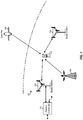
- FIG. 1 shows a wireless device 110 communicating with a wireless communication system 120.
- Wireless system 120 may be a Long Term Evolution (LTE) system, a Code Division Multiple Access (CDMA) system, a Global System for Mobile Communications (GSM) system, a wireless local area network (WLAN) system, or some other wireless system.
- LTE Long Term Evolution
- CDMA Code Division Multiple Access
- GSM Global System for Mobile Communications
- WLAN wireless local area network
- a CDMA system may implement Wideband CDMA (WCDMA), CDMA 1X, Time Division Synchronous CDMA (TD-SCDMA), or some other version of CDMA.
- WCDMA Wideband CDMA
- CDMA 1X Code Division Synchronous CDMA
- TD-SCDMA Time Division Synchronous CDMA
- FIG. 1 shows wireless system 120 including two base stations 130 and 132 and one system controller 140.
- a wireless system may include any number of base stations and any set of network entities.
- Wireless device 110 may also be referred to as a user equipment (UE), a mobile station, a terminal, an access terminal, a subscriber unit, a station, etc.
- Wireless device 110 may be a cellular phone, a smartphone, a tablet, a wireless modem, a personal digital assistant (PDA), a handheld device, a laptop computer, a smartbook, a netbook, a cordless phone, a wireless local loop (WLL) station, a Bluetooth device, etc.
- Wireless device 110 may be capable of communicating with wireless system 120.
- Wireless device 110 may also be capable of receiving signals from broadcast stations (e.g., a broadcast station 134), signals from satellites (e.g., a satellite 150) in one or more global navigation satellite systems (GNSS), etc.
- Wireless device 110 may support one or more radio technologies for wireless communication such as LTE, WCDMA, CDMA 1X, TD-SCDMA, GSM, 802.11, etc.
- Wireless device 110 may be able to operate in low-band (LB) covering frequencies lower than 1000 megahertz (MHz), mid-band (MB) covering frequencies from 1000 MHz to 2300 MHz, and/or high-band (HB) covering frequencies higher than 2300 MHz.
- low-band may cover 698 to 960 MHz
- mid-band may cover 1475 to 2170 MHz
- high-band may cover 2300 to 2690 MHz and 3400 to 3800 MHz.
- Low-band, mid-band, and high-band refer to three groups of bands (or band groups), with each band group including a number of frequency bands (or simply, "bands").
- Each band may cover up to 200 MHz and may include one or more carriers.
- Each carrier may cover up to 20 MHz in LTE.
- LTE Release 11 supports 35 bands, which are referred to as LTE/UMTS bands and are listed in 3GPP TS 36.101.
- Wireless device 110 may support carrier aggregation, which is operation on multiple carriers. Carrier aggregation may also be referred to as multi-carrier operation. Wireless device 110 may be configured with up to 5 carriers in one or two bands in LTE Release 11.
- carrier aggregation may be categorized into two types - intra-band CA and inter-band CA.
- Intra-band CA refers to operation on multiple carriers within the same band.
- Inter-band CA refers to operation on multiple carriers in different bands.
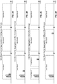
- FIG. 2A shows an example of contiguous intra-band CA.
- wireless device 110 is configured with three contiguous carriers in one band in low-band. Wireless device 110 may send and/or receive transmissions on the three contiguous carriers in the same band.
- FIG. 2B shows an example of non-contiguous intra-band CA.
- wireless device 110 is configured with three non-contiguous carriers in one band in low-band. The carriers may be separated by 5 MHz, 10 MHz, or some other amount. Wireless device 110 may send and/or receive transmissions on the three non-contiguous carriers in the same band.
- FIG. 2C shows an example of inter-band CA in the same band group.
- wireless device 110 is configured with three carriers in two bands in low-band. Wireless device 110 may send and/or receive transmissions on the three carriers in different bands in the same band group.
- FIG. 2D shows an example of inter-band CA in different band groups.
- wireless device 110 is configured with three carriers in two bands in different band groups, which include two carriers in one band in low-band and one carrier in another band in mid-band. Wireless device 110 may send and/or receive transmissions on the three carriers in different bands in different band groups.
- FIGS. 2A to 2D show four examples of carrier aggregation.
- Carrier aggregation may also be supported for other combinations of bands and band groups.
- FIG. 3 shows a block diagram of an exemplary design of wireless device 110 in FIG. 1 .
- wireless device 110 includes a data processor/ controller 310, a transceiver 320 coupled to a primary antenna 390, and a transceiver 322 coupled to a secondary antenna 392.
- Transceiver 320 includes K transmitters 330pa to 330pk, L receivers 380pa to 380pl, and an antenna interface circuit 370 to support multiple bands, carrier aggregation, multiple radio technologies, etc.
- K and L may each be any integer value of one or greater.
- Transceiver 322 includes M transmitters 330sa to 330sm, N receivers 380sa to 380sn, and an antenna interface circuit 372 to support multiple bands, carrier aggregation, multiple radio technologies, receive diversity, multiple-input multiple-output (MIMO) transmission, etc.
- M and N may each be any integer value of one or greater.
- each transmitter 330 includes a transmit circuit 340 and a power amplifier (PA) 360.
- data processor 310 processes (e.g., encodes and symbol maps) data to be transmitted to obtain modulation symbols.
- Data processor 310 further processes the modulation symbols (e.g., for OFDM, SC-FDMA, CDMA, or some other modulation technique) and provides I and Q samples for each transmit signal to be sent by wireless device 110.
- a transmit signal is a signal comprising a transmission on one or more carriers, a transmission on one or more frequency channels, etc.
- Data processor 310 provides the I and Q samples for one or more transmit signals to one or more selected transmitters.
- transmitter 330pa is a transmitter selected to send one transmit signal.
- transmit circuit 340pa converts I and Q samples to I and Q analog output signals, respectively.
- Transmit circuit 340pa further amplifies, filters, and upconverts the I and Q analog output signals from baseband to RF and provides a modulated RF signal.
- Transmit circuit 340pa may include digital-to-analog converters (DACs), amplifiers, filters, mixers, matching circuits, an oscillator, a local oscillator (LO) generator, a phase-locked loop (PLL), etc.
- a PA 360pa receives and amplifies the modulated RF signal and provides an output RF signal having the proper transmit power level.
- the output RF signal is routed through antenna interface circuit 370 and transmitted via antenna 390.
- Antenna interface circuit 370 may include one or more filters, duplexers, diplexers, switches, matching circuits, directional couplers, etc. Each remaining transmitter 330 in transceivers 320 and 322 may operate in similar manner as transmitter 330pa.
- each receiver 380 includes a low noise amplifier (LNA) 382 and a receive circuit 384.
- LNA low noise amplifier
- antenna 390 receives signals from base stations and/or other transmitter stations and provides a received RF signal, which is routed through antenna interface circuit 370 and provided to a selected receiver.
- LNA low noise amplifier
- receive circuit 384pa downconverts the amplified RF signal from RF to baseband, amplifies and filters the downconverted signal, and provides an analog input signal to data processor 310.
- Receive circuit 384pa may include mixers, filters, amplifiers, matching circuits, an oscillator, an LO generator, a PLL, etc. Each remaining receiver 380 in transceivers 320 and 322 may operate in similar manner as receiver 380pa.
- FIG. 3 shows an exemplary design of transmitters 330 and receivers 380.
- a transmitter and a receiver may also include other circuits not shown in FIG. 3 , such as filters, matching circuits, etc.
- All or a portion of transceivers 320 and 322 may be implemented on one or more analog integrated circuits (ICs), RF ICs (RFICs), mixed-signal ICs, etc.
- ICs analog integrated circuits
- RFICs RF ICs
- mixed-signal ICs etc.
- transmit circuits 340, LNAs 382, and receive circuits 384 may be implemented on one module, which may be an RFIC, etc.
- Antenna interface circuits 370 and 372 and PAs 360 may be implemented on another module, which may be a hybrid module, etc.
- the circuits in transceivers 320 and 322 may also be implemented in other manners.
- Data processor/controller 310 may perform various functions for wireless device 110. For example, data processor 310 may perform processing for data being transmitted via transmitters 330 and data being received via receivers 380. Controller 310 may control the operation of transmit circuits 340, PAs 360, LNAs 382, receive circuits 384, antenna interface circuits 370 and 372, or a combination thereof. A memory 312 may store program codes and data for data processor/controller 310. Data processor/controller 310 may be implemented on one or more application specific integrated circuits (ASICs) and/or other ICs.
- ASICs application specific integrated circuits
- Wireless device 110 may send multiple transmit signals simultaneously.
- the multiple transmit signals may be for transmissions on multiple contiguous or non-contiguous carriers with intra-band CA., e.g., as shown in FIG. 2A or 2B .
- each transmit signal may comprise a transmission sent on one carrier.
- the multiple transmit signals may be for transmissions on multiple frequency channels to the same wireless system.
- the multiple transmit signals may be for transmissions sent to different wireless systems (e.g., LTE and WLAN).
- data to be sent in each transmit signal may be processed (e.g., encoded, symbol mapped, and modulated) separately to generate I and Q samples for that transmit signal.
- Each transmit signal may be conditioned by a respective transmit circuit 340 and amplified by a respective PA 360 to generate an output RF signal for that transmit signal.
- a PA may receive a modulated RF signal and a power supply voltage and may generate an output RF signal.
- the output RF signal typically tracks the modulated RF signal and has a time-varying envelope.
- the power supply voltage should be higher than the amplitude of the output RF signal at all times in order to avoid clipping the output RF signal, which would then cause intermodulation distortion (IMD) that may degrade performance.
- IMD intermodulation distortion
- the difference between the power supply voltage and the envelope of the output RF signal represents wasted power that is dissipated by the PA instead of delivered to an output load.
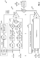
- FIG. 4 shows a design of a transmit module 400 supporting simultaneous transmission of multiple (K) transmit signals with a separate PA and separate power tracking for each transmit signal.
- Transmit module 400 includes K transmitters 430a to 430k that can simultaneously process K transmit signals, with each transmitter 430 processing one transmit signal.
- Each transmitter 430 includes a transmit circuit 440, a PA 460, and a power tracking supply generator 480.
- Transmitter 430a receives I 1 and Q 1 samples for a first transmit signal and generates a first output RF signal for the first transmit signal.
- the I 1 and Q 1 samples are provided to both transmit circuit 440a and voltage generator 480a.
- the I 1 and Q 1 samples are converted to I and Q analog signals by DACs 442a and 443a, respectively.
- the I analog signal is filtered by a lowpass filter 444a, amplified by an amplifier (Amp) 446a, and upconverted from baseband to RF by a mixer 448a.
- the Q analog signal is filtered by a lowpass filter 445a, amplified by an amplifier 447a, and upconverted from baseband to RF by a mixer 449a.
- Mixers 448a and 449a perform upconversion for the first transmit signal based on I and Q LO signals (ILO 1 and QLO 1 ) at a center RF frequency of the first transmit signal.
- a summer 450a sums the I and Q upconverted signals from mixers 448a and 449a to obtain a modulated RF signal, which is provided to PA 460a.
- a power tracker 482a receives the I 1 and Q 1 samples for the first transmit signal, computes the power of the first transmit signal based on the I 1 and Q 1 samples, and provides a digital power tracking signal to a DAC 484a.
- DAC 484a converts the digital power tracking signal to analog and provides an analog power tracking signal.
- a power supply generator 486a receives the analog power tracking signal and generates a power supply voltage for PA 460a.
- PA 460a amplifies the modulated RF signal from transmit circuit 440a using the power supply voltage from supply generator 486a and provides the first output RF signal for the first transmit signal.
- Each remaining transmitter 430 may similarly process I and Q samples for a respective transmit signal and may provide an output RF signal for the transmit signal.
- Up to K PAs 460a to 460k may provide up to K output RF signals at different RF frequencies for up to K transmit signals being sent simultaneously.
- a summer 462 receives the output RF signals being sent simultaneously, sums the output RF signals, and provides a final output RF signal, which is routed through a duplexer 470 and transmitted via an antenna 490.
- power tracking may be used to improve the efficiency of PAs 460a to 460k.
- Each transmit signal may be processed by a respective transmitter 430 using a separate sets of mixers 448 and 449 and PA 460.
- Multiple transmit signals may be sent on different frequencies (e.g., different carriers) and hence may have increased envelope bandwidth.
- the increased envelope bandwidth may be addressed by using a separate transmitter 430 for each transmit signal.
- Each transmitter 430 may then handle the envelope bandwidth of one transmit signal.
- operating multiple transmitters 430 concurrently for multiple transmit signals may result in more circuits, higher power consumption, and increased cost, all of which are undesirable.
- a single PA with power tracking may be used to generate a single output RF signal for multiple transmit signals being sent simultaneously.
- a single power supply voltage may be generated for the PA to track the power of all transmit signals being sent simultaneously. This may reduce the number of circuit components, reduce power consumption, and provide other advantages.
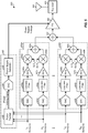
- FIG. 5 shows a design of a transmit module 500 supporting simultaneous transmission of multiple (K) transmit signals with a single PA and power tracking for all transmit signals.
- Transmit module 500 performs frequency upconversion separately for each transmit signal in the analog domain and sums the resultant upconverted RF signals for all transmit signals.
- Transmit module 500 includes K transmit circuits 540a to 540k that can simultaneously process K transmit signals, with each transmit circuit 540 processing one transmit signal.
- Transmit module 500 further includes a summer 552, a PA 560, a duplexer 570, and a power tracking supply generator 580.
- Transmit circuit 540a receives I 1 and Q 1 samples for a first transmit signal and generates a first upconverted RF signal for the first transmit signal.
- the I 1 and Q 1 samples are provided to both transmit circuit 540a and voltage generator 580.
- the I 1 and Q 1 samples are converted to I and Q analog signals by DACs 542a and 543a, respectively.
- the I and Q analog signals are filtered by lowpass filters 544a and 545a, amplified by amplifiers 546a and 547a, upconverted from baseband to RF by mixers 548a and 549a, and summed by a summer 550a to generate the first upconverted RF signal.
- Mixers 548a and 549a perform upconversion for the first transmit signal based on I and Q LO signals at a center RF frequency of the first transmit signal.
- Each remaining transmit circuit 540 may similarly process I and Q samples for a respective transmit signal and may provide an upconverted RF signal for the transmit signal.
- Up to K transmit circuits 540a to 540k may provide up to K upconverted RF signals at different RF frequencies for up to K transmit signals being sent simultaneously.
- a summer 552 receives the upconverted RF signals from transmit circuits 540a to 540k, sums the upconverted RF signals, and provides a modulated RF signal to PA 560.
- a power tracker 582 receives I 1 to I K samples and Q 1 to Q K samples for all transmit signals being sent simultaneously. Power tracker 582 computes the overall power of all transmit signals based on the I and Q samples for these transmit signals and provides a digital power tracking signal to a DAC 584. DAC 584 converts the digital power tracking signal to analog and provides an analog power tracking signal for all transmit signals. Although not shown in FIG. 5 , a lowpass filter may receive and filter an output signal from DAC 584 and provide the analog power tracking signal. A power supply generator 586 receives the analog power tracking signal and generates a power supply voltage for PA 560.
- PA 560 amplifies the modulated RF signal from summer 552 using the power supply voltage from supply generator 586. PA 560 provides an output RF signal for all transmit signals being sent simultaneously. The output RF signal is routed through duplexer 570 and transmitted via antenna 590.
- FIG. 6 shows a design of a transmit module 502 supporting simultaneous transmission of multiple (K) transmit signals with a single PA and power tracking for all transmit signals.
- Transmit module 502 digitally upconverts each transmit signal to an intermediate frequency (IF) in the digital domain, sums the resultant upconverted IF signals for all transmit signals, and performs frequency upconversion from IF to RF for all transmit signals together in the analog domain.
- Transmit module 502 includes a digital modulator 520, a transmit circuit 540, PA 560, duplexer 570, and power tracking supply generator 580.
- Digital modulator 520 receives I and Q samples for all transmit signals and generates a modulated IF signal for all transmit signals.
- the I 1 and Q 1 samples for the first transmit signal are upconverted to a first IF frequency by multipliers 522a and 523a, respectively, based on C I1 and C Q1 ) digital LO signals.
- the I and Q samples for each remaining transmit signal are upconverted to a different IF frequency by multipliers 522 and 523, respectively, for that transmit signal.
- the IF frequencies of the K transmit signals may be selected based on the final RF frequencies of the K transmit signals.
- a summer 524 sums the outputs of all K multipliers 522a to 522k and provides an I modulated signal.
- a summer 525 sums the outputs of all K multipliers 523a to 523k and provides a Q modulated signal.
- the I and Q modulated signals from summers 524 and 525 form the modulated IF signal for all transmit signals.
- Transmit circuit 540 receives I and Q modulated signals from digital modulator 520 and generates a modulated RF signal for all transmit signals.
- the I and Q modulated signals are converted to I and Q analog signals by DACs 542 and 543, respectively.
- the I and Q analog signals are filtered by lowpass filters 544 and 545, amplified by amplifiers 546 and 547, upconverted from IF to RF by mixers 548 and 549, and summed by a summer 550 to generate the modulated RF signal.
- Mixers 548 and 549 perform upconversion for the modulated IF signal based on I and Q LO signals at a suitable frequency so that the K transmit signals are upconverted to their proper RF frequencies.
- Power tracking voltage generator 580 receives the I 1 to I K samples and the Q 1 to Q K samples for all transmit signals being sent simultaneously. Voltage generator 580 generates a power supply voltage for PA 560 based on the I and Q samples. PA 560 amplifies the modulated RF signal from transmit circuit 540 using the power supply voltage from supply generator 580. PA 560 provides an output RF signal for all transmit signals being sent simultaneously. The output RF signal is routed through duplexer 570 and transmitted via antenna 590.
- FIGS. 5 and 6 show two exemplary designs of a transmit module supporting simultaneous transmission of multiple transmit signals with a single PA and power tracking for all transmit signals. Multiple transmit signals may also be sent with a single PA and power tracking in other manners. For example, polar modulation may be used instead of quadrature modulation, which is shown in FIGS. 5 and 6 .
- Power tracker 582 may compute the digital power tracking signal based on the I and Q samples for all transmit signals in various manners.
- the quantity I k 2 t + Q k 2 t denotes the power of the k-th transmit signal in sample period t.
- the powers of all transmit signals are summed to obtain an overall power.
- the digital power tracking signal is then obtained by taking the square root of the overall power.
- the scaling factor of K accounts for conversion between power and voltage.
- the quantity I k 2 t + Q k 2 t denotes the voltage of the k-th transmit signal in sample period t.
- the voltage of each transmit signal is first computed, and the voltages of all transmit signals are then summed to obtain the digital power tracking signal.
- Equations (1) and (2) are two exemplary designs of computing the digital power tracking signal based on the I and Q samples for all transmit signals being sent simultaneously.
- the digital power tracking signal computed in equation (1) or (2) has a bandwidth that approximates the bandwidth of the widest transmit signal (instead of the overall bandwidth of all transmit signals being sent simultaneously). Having the bandwidth of the power tracking signal being smaller than a modulation bandwidth may allow for a more efficient power tracking circuitry and may also result in less noise being injected into PA 560 via the power supply.
- the digital power tracking signal may also be computed based on the I and Q samples of the transmit signals in other manners, e.g., based on other equations or functions.
- the digital power tracking signal may be generated based on the I and Q samples for all transmit signals, without any filtering, e.g., as shown in equation (1) or (2).
- the digital power tracking signal may be filtered, e.g., with a lowpass filter having similar characteristics as lowpass filters 544 and 545 in transmit circuit 540.
- the digital power tracking signal may be computed in the same manner (e.g., based on the same equation) regardless of the number of transmit signals being sent simultaneously. In another design, the digital power tracking signal may be computed in different manners (e.g., based on different equations) depending on the number of transmit signals being sent simultaneously. The digital power tracking signal may also be computed in different manners depending on other factors such as the transmit power levels of different transmit signals.
- the techniques described herein for generating a power tracking supply voltage for multiple transmit signals may be used for various modulation techniques.
- the techniques may be used to generate a power tracking supply voltage for multiple transmit signals sent simultaneously using orthogonal frequency division multiplexing (OFDM), SC-FDMA, CDMA, or some other modulation techniques.
- OFDM orthogonal frequency division multiplexing
- SC-FDMA SC-FDMA
- CDMA Code Division Multiple Access
- the techniques may also be used to generate a tracking power supply voltage for any number of transmit signals being sent simultaneously.
- FIG. 7A shows an example of power tracking for two transmit signals sent on two non-contiguous carriers with SC-FDMA, e.g., for non-contiguous intra-band CA shown in FIG. 2B .
- the two transmit signals are sent on two carriers separated by a 25 MHz gap, with each carrier having a bandwidth of 10 MHz.
- a plot 710 shows an output RF signal comprising the two transmit signals and provided by PA 560 in FIG. 5 or 6 .
- a plot 712 shows a power tracking signal provided by power tracker 582 in FIG. 5 or 6 .
- the power tracking signal is computed based on I and Q samples for the two transmit signals in accordance with equation (1). As shown in FIG. 7A , the power tracking signal closely follows the envelope of the output RF signal. Hence, good performance and high efficiency may be achieved for PA 560.
- FIG. 7B shows an example of power tracking for three transmit signals sent on three non-contiguous carriers with OFDM, e.g., for non-contiguous intra-band CA.
- the three transmit signals are sent on three carriers, with each carrier having a bandwidth of 5 MHz and being separated by a 15 MHz gap to another carrier.
- a plot 720 shows an output RF signal comprising the three transmit signals and provided by PA 560 in FIG. 5 or 6 .
- a plot 722 shows a power tracking signal provided by power tracker 582 in FIG. 5 or 6 .
- the power tracking signal is computed based on I and Q samples for the three transmit signals in accordance with equation (1). As shown in FIG. 7B , the power tracking signal follows the envelope of the output RF signal. Hence, good performance and high efficiency may be achieved for PA 560.
- a power tracking supply voltage may also be generated for multiple transmit signals sent on multiple carriers with CDMA.
- the power tracking supply voltage can closely follow the envelope of the output RF signal when two transmit signals are sent simultaneously, e.g., as shown in FIG. 7A .
- the power tracking supply voltage can approximate the envelope of the output RF signal when more than two transmit signals are sent simultaneously, e.g., as shown in FIG. 7B .
- Power supply generator 586 may generate a power supply voltage for PA 560 based on a power tracking signal in various manners. Power supply generator 586 should generate the power supply voltage in an efficient manner in order to conserve battery power of wireless device 110.
- FIG. 8 shows a design of power supply generator 586 in FIGS. 5 and 6 .
- power supply generator 586 includes a power tracking amplifier (PT Amp) 810, a switcher 820, a boost converter 830, and an inductor 822.
- Switcher 820 may also be referred to as a switching-mode power supply (SMPS).
- Switcher 820 receives a battery voltage (V BAT ) and provides a first supply current (I SW ) comprising DC and low frequency components at node A.
- Inductor 822 stores current from switcher 820 and provides the stored current to node A on alternating cycles.
- Boost converter 830 receives the V BAT voltage and generates a boosted supply voltage (V BOOST ) that is higher than the V BAT voltage.
- V BOOST boosted supply voltage
- Power tracking amplifier 810 receives the analog power tracking signal at its signal input, receives the V BAT voltage and the V BOOST voltage at its two power supply inputs, and provides a second supply current (I PT ) comprising high frequency components at node A.
- the PA supply current (I PA ) provided to power amplifier 560 includes the I SW current from switcher 820 and the I PT current from power tracking amplifier 810.
- Power tracking amplifier 810 also provides the proper PA supply voltage (V PA ) at Node A for PA 560.
- V PA PA supply voltage
- FIG. 9 shows a schematic diagram of a design of power tracking amplifier 810 and switcher 820 within power supply generator 586 in FIG. 8 .
- an operational amplifier (op-amp) 910 has its non-inverting input receiving the power tracking signal, its inverting input coupled to an output of power tracking amplifier 810 (which is node X), and its output coupled to an input of a class AB driver 912.
- Driver 912 has its first output (R1) coupled to the gate of a P-channel metal oxide semiconductor (PMOS) transistor 914 and its second output (R2) coupled to the gate of an N-channel metal oxide semiconductor (NMOS) transistor 916.
- NMOS transistor 916 has its drain coupled to node X and its source coupled to circuit ground.
- PMOS transistor 914 has its drain coupled to node X and its source coupled to the drains of PMOS transistors 918 and 920.
- PMOS transistor 918 has its gate receiving a C1 control signal and its source receiving the V BOOST voltage.
- PMOS transistor 920 has its gate receiving a C2 control signal and its source receiving the V BAT voltage.
- a current sensor 824 is coupled between node X and node A and senses the I PT current provided by power tracking amplifier 810. Sensor 824 passes most of the I PT current to node A and provides a small fraction of the I PT current as a sensed current (I SEN ) to switcher 820.
- a current sense amplifier 930 has its input coupled to current sensor 824 and its output coupled to an input of a switcher driver 932.
- Driver 932 has its first output (S1) coupled to the gate of a PMOS transistor 934 and its second output (S2) coupled to the gate of an NMOS transistor 936.
- NMOS transistor 936 has its drain coupled to an output of switcher 820 (which is node Y) and its source coupled to circuit ground.
- PMOS transistor 934 has its drain coupled to node Y and its source receiving the V BAT voltage.
- Inductor 822 is coupled between node A and node Y.
- Switcher 820 operates as follows. Switcher 820 is in an ON state when current sensor 824 senses a high output current from power tracking amplifier 810 and provides a low sensed voltage to driver 932. Driver 932 then provides a low voltage to the gate of PMOS transistor 934 and a low voltage to the gate of NMOS transistor 936. PMOS transistor 934 is turned ON and couples the V BAT voltage to inductor 822, which stores energy from the V BAT voltage. The current through inductor 822 rises during the ON state, with the rate of the rise being dependent on (i) the difference between the V BAT voltage and the V PA voltage at node A and (ii) the inductance of inductor 822.
- switcher 820 is in an OFF state when current sensor 824 senses a low output current from power tracking amplifier 810 and provides a high sensed voltage to driver 932.
- Driver 932 then provides a high voltage to the gate of PMOS transistor 934 and a high voltage to the gate of NMOS transistor 936.
- NMOS transistor 936 is turned ON, and inductor 822 is coupled between node A and circuit ground.
- the current through inductor 822 falls during the OFF state, with the rate of the fall being dependent on the V PA voltage at node A and the inductance of inductor 822.
- the V BAT voltage thus provides current to PA 560 via inductor 822 during the ON state, and inductor 120 provides its stored energy to PA 560 during the OFF state.
- Power tracking amplifier 810 operates as follows. When the power tracking signal increases, the output of op-amp 910 increases, the R1 output of driver 912 deceases and the R2 output of driver 912 decreases until NMOS transistor 916 is almost turned OFF, and the output of power tracking amplifier 810 increases. The converse is true when the power tracking signal decreases. The negative feedback from the output of power tracking amplifier 810 to the inverting input of op-amp 910 results in power tracking amplifier 810 having unity gain. Hence, the output of power tracking amplifier 810 follows the power tracking signal, and the V PA voltage is approximately equal to the power tracking signal.
- Driver 912 may be implemented with a class AB amplifier to improve efficiency, so that large output currents can be supplied even though the bias current in transistors 914 and 916 is low.
- power tracking amplifier 810 operates based on the V BOOST voltage only when needed and based on the V BAT voltage during the remaining time in order to improve efficiency. For example, power tracking amplifier 810 may provide approximately 85% of the power based on the V BAT voltage and only approximately 15% of the power based on the V BOOST voltage.
- boost converter 830 is enabled and generates the V BOOST voltage, PMOS transistor 918 is turned ON and provides the V BOOST voltage to the source of PMOS transistor 914, and PMOS transistor 920 is turned OFF.
- the C1 control signal is at logic high, and the C2 control signal is at logic low.
- boost converter 830 is disabled, PMOS transistor 918 is turned OFF, and PMOS transistor 920 is turned ON and provides the V BAT voltage to the source of PMOS transistor 914.
- a control signal generator 940 receives the power tracking signal and the V BAT voltage and generates the C1 and C2 control signals.
- the C1 control signal is complementary to the C2 control signal.
- generator 940 generates the C1 and C2 control signals to select the V BOOST voltage for power tracking amplifier 910 when the magnitude of the power tracking signal exceeds a first threshold.
- the first threshold may be a fixed threshold or may be determined based on the V BAT voltage.
- generator 940 generates the C1 and C2 control signals to select the V BOOST voltage for power tracking amplifier 910 when the magnitude of the power tracking signal exceeds the first threshold and the V BAT voltage is below a second threshold.
- Generator 940 may also generate the C1 and C2 signals based on other signals, other voltages, and/or other criteria.
- Switcher 820 has high efficiency and delivers a majority of the supply current for PA 560.
- Power tracking amplifier 810 operates as a linear stage and has relatively high bandwidth (e.g., in the MHz range).
- Switcher 820 operates to reduce the output current from power tracking amplifier 810, which improves overall efficiency.
- FIG. 9 shows an exemplary design of switcher 820 and power tracking amplifier 810 in FIG. 1 .
- Switcher 820 and power tracking amplifier 810 may also be implemented in other manners.
- power tracking amplifier 810 may be implemented as described in U.S. Patent No. 6,300,826 , entitled “Apparatus and Method for Efficiently Amplifying Wideband Envelope Signals,” issued October 9, 2001.
- an apparatus e.g., an integrated circuit, a wireless device, a circuit module, etc.
- the power tracker e.g., power tracker 582 in FIG. 5
- the power supply generator may generate a power supply voltage based on the power tracking signal.
- the power tracker may determine an overall power of the plurality of transmit signals based on the I and Q components of the plurality of transmit signals, e.g., as I l 2 t + Q l 2 t + ... + I K 2 t + Q K 2 t .
- the power tracker may then determine the power tracking signal based on the overall power of the plurality of transmit signals, e.g., as shown in equation (1).
- the power tracker may determine the power of each transmit signal based on the I and Q components of that transmit signal, e.g., as I k 2 t + Q k 2 t for the k-th transmit signal.
- the power tracker may then determine the power tracking signal based on the powers of the plurality of transmit signals, e.g., as shown in equation (2).
- the power tracker may determine a voltage of each transmit signal based on the power of the transmit signal, e.g., as I k 2 t + Q k 2 t .
- the power tracker may then determine the power tracking signal based on voltages of the plurality of transmit signals, e.g., as shown in equation (2).
- the power tracker may also determine the power tracking signal based on the I and Q components of the plurality of transmit signals in other manners.
- the plurality of transmit signals may be sent on a plurality of carriers at different frequencies.
- the power tracking signal may have a bandwidth that is smaller than an overall bandwidth of the plurality of carriers.
- the apparatus may comprise a plurality of transmit circuits and a summer, e.g., as shown in FIG. 5 .
- the plurality of transmit circuits (e.g., transmit circuits 540a to 540k) may receive the I and Q components of the plurality of transmit signals and may provide a plurality of upconverted RF signals.
- Each transmit circuit may upconvert I and Q components of one transmit signal and provide a corresponding upconverted RF signal.
- the summer e.g., summer 552 may sum the plurality of upconverted RF signals and provide a modulated RF signal.
- the apparatus may comprise a transmit circuit (e.g., transmit circuit 540 in FIG.
- the apparatus may further comprise a PA (e.g., PA 560 in FIGS. 5 and 6 ) that may amplify the modulated RF signal based on the power supply voltage and provide an output RF signal.
- a PA e.g., PA 560 in FIGS. 5 and 6
- the power supply generator may comprise a power tracking amplifier (e.g., power tracking amplifier 810 in FIGS. 8 and 9 ) that may receive the power tracking signal and generate the power supply voltage.
- the power supply generator may further comprise a switcher and/or a boost converter.
- the switcher e.g., switcher 820 in FIGS. 8 and 9
- the boost converter may receive a battery voltage and provide a boosted voltage for the power tracking amplifier.
- the power tracking amplifier may operate based on the boosted voltage or the battery voltage.
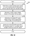
- FIG. 10 shows a design of a process 1000 for generating a power supply voltage with power tracking.
- a power tracking signal may be determined based on I and Q components of a plurality of transmit signals being sent simultaneously (block 1012).
- an overall power of the plurality of transmit signals may be determined based on the I and Q components of the plurality of transmit signals.
- the power tracking signal may then be determined based on the overall power of the plurality of transmit signals, e.g., as shown in equation (1).
- the power of each transmit signal may be determined based on the I and Q components of the transmit signal.
- the power tracking signal may then be determined based on the powers of the plurality of transmit signals, e.g., as shown in equation (2).
- a power supply voltage may be generated based on the power tracking signal (block 1014).
- the power supply voltage may be generated with a amplifier (e.g., amplifier 810 in FIG. 9 ) that tracks the power tracking signal.
- the power supply voltage may also be generated based on a switcher and/or a boost converter.
- a modulated RF signal may be generated based on the I and Q components of the plurality of transmit signals (block 1016).
- I and Q components of each transmit signal may be upconverted to obtain a corresponding upconverted RF signal.
- a plurality of upconverted RF signals for the plurality of transmit signals may then be summed to obtain the modulated RF signal, e.g., as shown in FIG. 5 .
- a modulated IF signal may be generated based on the I and Q components of the plurality of transmit signals, e.g., as shown in FIG. 6 .
- the modulated IF signal may then be upconverted to obtain the modulated RF signal.
- the modulated RF signal may be amplified with a PA (e.g., PA 560 in FIGS. 5 and 6 ) operating based on the power supply voltage to obtain an output RF signal (block 1018).
- PA e.g., PA 560 in FIGS. 5 and 6
- the power tracker and power supply generator described herein may be implemented on an IC, an analog IC, an RFIC, a mixed-signal IC, an ASIC, a printed circuit board (PCB), an electronic device, etc.
- the power tracker and power supply generator may also be fabricated with various IC process technologies such as complementary metal oxide semiconductor (CMOS), NMOS, PMOS, bipolar junction transistor (BJT), bipolar-CMOS (BiCMOS), silicon germanium (SiGe), gallium arsenide (GaAs), etc.
- CMOS complementary metal oxide semiconductor
- NMOS NMOS
- PMOS bipolar junction transistor
- BiCMOS bipolar-CMOS
- SiGe silicon germanium
- GaAs gallium arsenide
- An apparatus implementing the power tracker and/or power supply generator described herein may be a stand-alone device or may be part of a larger device.
- a device may be (i) a stand-alone IC, (ii) a set of one or more ICs that may include memory ICs for storing data and/or instructions, (iii) an RFIC such as an RF receiver (RFR) or an RF transmitter/receiver (RTR), (iv) an ASIC such as a mobile station modem (MSM), (v) a module that may be embedded within other devices, (vi) a receiver, cellular phone, wireless device, handset, or mobile unit, (vii) etc.
- RFR RF receiver
- RTR RF transmitter/receiver
- MSM mobile station modem
- the functions described may be implemented in hardware, software, firmware, or any combination thereof. If implemented in software, the functions may be stored on or transmitted over as one or more instructions or code on a computer-readable medium.
- Computer-readable media includes both computer storage media and communication media including any medium that facilitates transfer of a computer program from one place to another.
- a storage media may be any available media that can be accessed by a computer.
- such computer-readable media can comprise RAM, ROM, EEPROM, CD-ROM or other optical disk storage, magnetic disk storage or other magnetic storage devices, or any other medium that can be used to carry or store desired program code in the form of instructions or data structures and that can be accessed by a computer.
- any connection is properly termed a computer-readable medium.
- the software is transmitted from a website, server, or other remote source using a coaxial cable, fiber optic cable, twisted pair, digital subscriber line (DSL), or wireless technologies such as infrared, radio, and microwave
- the coaxial cable, fiber optic cable, twisted pair, DSL, or wireless technologies such as infrared, radio, and microwave are included in the definition of medium.
- Disk and disc includes compact disc (CD), laser disc, optical disc, digital versatile disc (DVD), floppy disk and blu-ray disc where disks usually reproduce data magnetically, while discs reproduce data optically with lasers. Combinations of the above should also be included within the scope of computer-readable media.
Landscapes
- Engineering & Computer Science (AREA)
- Power Engineering (AREA)
- Computer Networks & Wireless Communication (AREA)
- Signal Processing (AREA)
- Microelectronics & Electronic Packaging (AREA)
- Physics & Mathematics (AREA)
- Nonlinear Science (AREA)
- Transmitters (AREA)
- Amplifiers (AREA)
Description
- The present disclosure claims priority to
U.S. Nonprovisional App. No. 13/764,328 filed February 11, 2013 - The present disclosure relates generally to electronics, and more specifically to techniques for generating a power supply voltage for a circuit such as an amplifier.
- A wireless device (e.g., a cellular phone or a smartphone) in a wireless communication system may transmit and receive data for two-way communication. The wireless device may include a transmitter for data transmission and a receiver for data reception. For data transmission, the transmitter may process (e.g., encode and modulate) data to generate output samples. The transmitter may further condition (e.g., convert to analog, filter, amplify, and frequency upconvert) the output samples to generate a modulated radio frequency (RF) signal, amplify the modulated RF signal to obtain an output RF signal having the proper transmit power level, and transmit the output RF signal via an antenna to a base station. For data reception, the receiver may obtain a received RF signal via the antenna and may amplify and process the received RF signal to recover data sent by the base station.
- The transmitter typically includes a power amplifier (PA) to provide high transmit power for the output RF signal. The power amplifier should be able to provide high transmit power and have high power-added efficiency (PAE).
Attention is drawn todocument GB 2 476 393 A document GB 2 488 380 A
Finally, attention is drawn to documentUS 2012/326783 A1 which relates to techniques for efficiently generating a power supply. For example, an apparatus includes an envelope amplifier and a boost converter. The boost converter generates a boosted supply voltage having a higher voltage than a first supply voltage (e.g., a battery voltage). The envelope amplifier generates a second supply voltage based on an envelope signal and the boosted supply voltage (and also possibly the first supply voltage). A power amplifier operates based on the second supply voltage. In a further example, an apparatus includes a switcher, an envelope amplifier, and a power amplifier. The switcher receives a first supply voltage and provides a first supply current. The envelope amplifier provides a second supply current based on an envelope signal. The power amplifier receives a total supply current including the first and second supply currents. - In accordance with the present invention, an apparatus, as set forth in
claim 1, and a method, as set forth in claim 13, is provided. Further embodiments are claimed in the dependent claims. Techniques for generating a power tracking supply voltage for a circuit (e.g., a power amplifier) that processes multiple transmit signals sent simultaneously are disclosed herein. The multiple transmit signals may comprise transmissions sent simultaneously on multiple carriers at different frequencies. - In one exemplary design, an apparatus includes a power tracker and a power supply generator. The power tracker determines a power tracking signal based on inphase (I) and quadrature (Q) components of a plurality of transmit signals being sent simultaneously, as described below. The power supply generator generates a power supply voltage based on the power tracking signal. The apparatus may further include a power amplifier that amplifies a modulated RF signal based on the power supply voltage and provides an output RF signal.
- Various aspects and features of the disclosure are described in further detail below.
-
-
FIG. 1 shows a wireless device communicating with a wireless system. -
FIGS. 2A to 2D show four examples of carrier aggregation. -
FIG. 3 shows a block diagram of the wireless device inFIG. 1 . -
FIG. 4 shows a transmit module comprising a separate power amplifier with separate power tracking for each transmit signal. -
FIGS. 5 and6 show two designs of a transmit module comprising a single power amplifier with power tracking for all transmit signals. -
FIGS. 7A and 7B show power tracking for two and three transmit signals, respectively. -
FIGS. 8 and9 show a design of a power supply generator with power tracking. -
FIG. 10 shows a process for generating a power supply voltage with power tracking. - The word "exemplary" is used herein to mean "serving as an example, instance, or illustration." Any design described herein as "exemplary" is not necessarily to be construed as preferred or advantageous over other designs.
- Techniques for generating a power tracking supply voltage for a circuit (e.g., a power amplifier) that processes multiple transmit signals sent simultaneously are disclosed herein. The techniques may be used for various electronic devices such as wireless communication devices.
-
FIG. 1 shows awireless device 110 communicating with awireless communication system 120.Wireless system 120 may be a Long Term Evolution (LTE) system, a Code Division Multiple Access (CDMA) system, a Global System for Mobile Communications (GSM) system, a wireless local area network (WLAN) system, or some other wireless system. A CDMA system may implement Wideband CDMA (WCDMA), CDMA 1X, Time Division Synchronous CDMA (TD-SCDMA), or some other version of CDMA. For simplicity,FIG. 1 showswireless system 120 including twobase stations system controller 140. In general, a wireless system may include any number of base stations and any set of network entities. -
Wireless device 110 may also be referred to as a user equipment (UE), a mobile station, a terminal, an access terminal, a subscriber unit, a station, etc.Wireless device 110 may be a cellular phone, a smartphone, a tablet, a wireless modem, a personal digital assistant (PDA), a handheld device, a laptop computer, a smartbook, a netbook, a cordless phone, a wireless local loop (WLL) station, a Bluetooth device, etc.Wireless device 110 may be capable of communicating withwireless system 120.Wireless device 110 may also be capable of receiving signals from broadcast stations (e.g., a broadcast station 134), signals from satellites (e.g., a satellite 150) in one or more global navigation satellite systems (GNSS), etc.Wireless device 110 may support one or more radio technologies for wireless communication such as LTE, WCDMA, CDMA 1X, TD-SCDMA, GSM, 802.11, etc. -
Wireless device 110 may be able to operate in low-band (LB) covering frequencies lower than 1000 megahertz (MHz), mid-band (MB) covering frequencies from 1000 MHz to 2300 MHz, and/or high-band (HB) covering frequencies higher than 2300 MHz. For example, low-band may cover 698 to 960 MHz, mid-band may cover 1475 to 2170 MHz, and high-band may cover 2300 to 2690 MHz and 3400 to 3800 MHz. Low-band, mid-band, and high-band refer to three groups of bands (or band groups), with each band group including a number of frequency bands (or simply, "bands"). Each band may cover up to 200 MHz and may include one or more carriers. Each carrier may cover up to 20 MHz in LTE. LTE Release 11 supports 35 bands, which are referred to as LTE/UMTS bands and are listed in 3GPP TS 36.101. -
Wireless device 110 may support carrier aggregation, which is operation on multiple carriers. Carrier aggregation may also be referred to as multi-carrier operation.Wireless device 110 may be configured with up to 5 carriers in one or two bands in LTE Release 11. - In general, carrier aggregation (CA) may be categorized into two types - intra-band CA and inter-band CA. Intra-band CA refers to operation on multiple carriers within the same band. Inter-band CA refers to operation on multiple carriers in different bands.
-
FIG. 2A shows an example of contiguous intra-band CA. In the example shown inFIG. 2A ,wireless device 110 is configured with three contiguous carriers in one band in low-band.Wireless device 110 may send and/or receive transmissions on the three contiguous carriers in the same band. -
FIG. 2B shows an example of non-contiguous intra-band CA. In the example shown inFIG. 2B ,wireless device 110 is configured with three non-contiguous carriers in one band in low-band. The carriers may be separated by 5 MHz, 10 MHz, or some other amount.Wireless device 110 may send and/or receive transmissions on the three non-contiguous carriers in the same band. -
FIG. 2C shows an example of inter-band CA in the same band group. In the example shown inFIG. 2C ,wireless device 110 is configured with three carriers in two bands in low-band.Wireless device 110 may send and/or receive transmissions on the three carriers in different bands in the same band group. -
FIG. 2D shows an example of inter-band CA in different band groups. In the example shown inFIG. 2D ,wireless device 110 is configured with three carriers in two bands in different band groups, which include two carriers in one band in low-band and one carrier in another band in mid-band.Wireless device 110 may send and/or receive transmissions on the three carriers in different bands in different band groups. -
FIGS. 2A to 2D show four examples of carrier aggregation. Carrier aggregation may also be supported for other combinations of bands and band groups. -
FIG. 3 shows a block diagram of an exemplary design ofwireless device 110 inFIG. 1 . In this exemplary design,wireless device 110 includes a data processor/controller 310, atransceiver 320 coupled to aprimary antenna 390, and atransceiver 322 coupled to asecondary antenna 392.Transceiver 320 includes K transmitters 330pa to 330pk, L receivers 380pa to 380pl, and anantenna interface circuit 370 to support multiple bands, carrier aggregation, multiple radio technologies, etc. K and L may each be any integer value of one or greater.Transceiver 322 includes M transmitters 330sa to 330sm, N receivers 380sa to 380sn, and anantenna interface circuit 372 to support multiple bands, carrier aggregation, multiple radio technologies, receive diversity, multiple-input multiple-output (MIMO) transmission, etc. M and N may each be any integer value of one or greater. - In the exemplary design shown in
FIG. 3 , each transmitter 330 includes a transmit circuit 340 and a power amplifier (PA) 360. For data transmission,data processor 310 processes (e.g., encodes and symbol maps) data to be transmitted to obtain modulation symbols.Data processor 310 further processes the modulation symbols (e.g., for OFDM, SC-FDMA, CDMA, or some other modulation technique) and provides I and Q samples for each transmit signal to be sent bywireless device 110. A transmit signal is a signal comprising a transmission on one or more carriers, a transmission on one or more frequency channels, etc.Data processor 310 provides the I and Q samples for one or more transmit signals to one or more selected transmitters. The description below assumes that transmitter 330pa is a transmitter selected to send one transmit signal. Within transmitter 330pa, transmit circuit 340pa converts I and Q samples to I and Q analog output signals, respectively. Transmit circuit 340pa further amplifies, filters, and upconverts the I and Q analog output signals from baseband to RF and provides a modulated RF signal. Transmit circuit 340pa may include digital-to-analog converters (DACs), amplifiers, filters, mixers, matching circuits, an oscillator, a local oscillator (LO) generator, a phase-locked loop (PLL), etc. A PA 360pa receives and amplifies the modulated RF signal and provides an output RF signal having the proper transmit power level. The output RF signal is routed throughantenna interface circuit 370 and transmitted viaantenna 390.Antenna interface circuit 370 may include one or more filters, duplexers, diplexers, switches, matching circuits, directional couplers, etc. Each remaining transmitter 330 intransceivers - In the exemplary design shown in
FIG. 3 , each receiver 380 includes a low noise amplifier (LNA) 382 and a receive circuit 384. For data reception,antenna 390 receives signals from base stations and/or other transmitter stations and provides a received RF signal, which is routed throughantenna interface circuit 370 and provided to a selected receiver. The description below assumes that receiver 380pa is the selected receiver. Within receiver 380pa, an LNA 382pa amplifies the received RF signal and provides an amplified RF signal. A receive circuit 384pa downconverts the amplified RF signal from RF to baseband, amplifies and filters the downconverted signal, and provides an analog input signal todata processor 310. Receive circuit 384pa may include mixers, filters, amplifiers, matching circuits, an oscillator, an LO generator, a PLL, etc. Each remaining receiver 380 intransceivers -
FIG. 3 shows an exemplary design of transmitters 330 and receivers 380. A transmitter and a receiver may also include other circuits not shown inFIG. 3 , such as filters, matching circuits, etc. All or a portion oftransceivers Antenna interface circuits transceivers - Data processor/
controller 310 may perform various functions forwireless device 110. For example,data processor 310 may perform processing for data being transmitted via transmitters 330 and data being received via receivers 380.Controller 310 may control the operation of transmit circuits 340, PAs 360, LNAs 382, receive circuits 384,antenna interface circuits memory 312 may store program codes and data for data processor/controller 310. Data processor/controller 310 may be implemented on one or more application specific integrated circuits (ASICs) and/or other ICs. -
Wireless device 110 may send multiple transmit signals simultaneously. In one design, the multiple transmit signals may be for transmissions on multiple contiguous or non-contiguous carriers with intra-band CA., e.g., as shown inFIG. 2A or 2B . For example, each transmit signal may comprise a transmission sent on one carrier. In another design, the multiple transmit signals may be for transmissions on multiple frequency channels to the same wireless system. In yet another design, the multiple transmit signals may be for transmissions sent to different wireless systems (e.g., LTE and WLAN). In any case, data to be sent in each transmit signal may be processed (e.g., encoded, symbol mapped, and modulated) separately to generate I and Q samples for that transmit signal. Each transmit signal may be conditioned by a respective transmit circuit 340 and amplified by a respective PA 360 to generate an output RF signal for that transmit signal. - A PA may receive a modulated RF signal and a power supply voltage and may generate an output RF signal. The output RF signal typically tracks the modulated RF signal and has a time-varying envelope. The power supply voltage should be higher than the amplitude of the output RF signal at all times in order to avoid clipping the output RF signal, which would then cause intermodulation distortion (IMD) that may degrade performance. The difference between the power supply voltage and the envelope of the output RF signal represents wasted power that is dissipated by the PA instead of delivered to an output load.
- It may be desirable to generate a power supply voltage for a PA such that good performance and good efficiency can be obtained. This may be achieved by generating the power supply voltage for the PA with power tracking so that the power supply voltage can track the envelope of an output RF signal from the PA.
-
FIG. 4 shows a design of a transmitmodule 400 supporting simultaneous transmission of multiple (K) transmit signals with a separate PA and separate power tracking for each transmit signal. Transmitmodule 400 includesK transmitters 430a to 430k that can simultaneously process K transmit signals, with each transmitter 430 processing one transmit signal. Each transmitter 430 includes a transmit circuit 440, a PA 460, and a power tracking supply generator 480. -
Transmitter 430a receives I1 and Q1 samples for a first transmit signal and generates a first output RF signal for the first transmit signal. The I1 and Q1 samples are provided to both transmitcircuit 440a andvoltage generator 480a. Within transmitcircuit 440a, the I1 and Q1 samples are converted to I and Q analog signals byDACs lowpass filter 444a, amplified by an amplifier (Amp) 446a, and upconverted from baseband to RF by amixer 448a. Similarly, the Q analog signal is filtered by alowpass filter 445a, amplified by anamplifier 447a, and upconverted from baseband to RF by amixer 449a.Mixers summer 450a sums the I and Q upconverted signals frommixers PA 460a. - Within
voltage generator 480a, apower tracker 482a receives the I1 and Q1 samples for the first transmit signal, computes the power of the first transmit signal based on the I1 and Q1 samples, and provides a digital power tracking signal to aDAC 484a.DAC 484a converts the digital power tracking signal to analog and provides an analog power tracking signal. Apower supply generator 486a receives the analog power tracking signal and generates a power supply voltage forPA 460a.PA 460a amplifies the modulated RF signal from transmitcircuit 440a using the power supply voltage fromsupply generator 486a and provides the first output RF signal for the first transmit signal. - Each remaining transmitter 430 may similarly process I and Q samples for a respective transmit signal and may provide an output RF signal for the transmit signal. Up to K PAs 460a to 460k may provide up to K output RF signals at different RF frequencies for up to K transmit signals being sent simultaneously. A
summer 462 receives the output RF signals being sent simultaneously, sums the output RF signals, and provides a final output RF signal, which is routed through aduplexer 470 and transmitted via anantenna 490. - As shown in
FIG. 4 , power tracking may be used to improve the efficiency of PAs 460a to 460k. Each transmit signal may be processed by a respective transmitter 430 using a separate sets of mixers 448 and 449 and PA 460. Multiple transmit signals may be sent on different frequencies (e.g., different carriers) and hence may have increased envelope bandwidth. The increased envelope bandwidth may be addressed by using a separate transmitter 430 for each transmit signal. Each transmitter 430 may then handle the envelope bandwidth of one transmit signal. However, operating multiple transmitters 430 concurrently for multiple transmit signals may result in more circuits, higher power consumption, and increased cost, all of which are undesirable. - In an aspect of the present disclosure, a single PA with power tracking may be used to generate a single output RF signal for multiple transmit signals being sent simultaneously. A single power supply voltage may be generated for the PA to track the power of all transmit signals being sent simultaneously. This may reduce the number of circuit components, reduce power consumption, and provide other advantages.
-
FIG. 5 shows a design of a transmitmodule 500 supporting simultaneous transmission of multiple (K) transmit signals with a single PA and power tracking for all transmit signals. Transmitmodule 500 performs frequency upconversion separately for each transmit signal in the analog domain and sums the resultant upconverted RF signals for all transmit signals. Transmitmodule 500 includes K transmitcircuits 540a to 540k that can simultaneously process K transmit signals, with each transmit circuit 540 processing one transmit signal. Transmitmodule 500 further includes asummer 552, aPA 560, aduplexer 570, and a powertracking supply generator 580. - Transmit
circuit 540a receives I1 and Q1 samples for a first transmit signal and generates a first upconverted RF signal for the first transmit signal. The I1 and Q1 samples are provided to both transmitcircuit 540a andvoltage generator 580. Within transmitcircuit 540a, the I1 and Q1 samples are converted to I and Q analog signals byDACs lowpass filters amplifiers mixers summer 550a to generate the first upconverted RF signal.Mixers - Each remaining transmit circuit 540 may similarly process I and Q samples for a respective transmit signal and may provide an upconverted RF signal for the transmit signal. Up to K transmit
circuits 540a to 540k may provide up to K upconverted RF signals at different RF frequencies for up to K transmit signals being sent simultaneously. Asummer 552 receives the upconverted RF signals from transmitcircuits 540a to 540k, sums the upconverted RF signals, and provides a modulated RF signal toPA 560. - Within
voltage generator 580, apower tracker 582 receives I1 to IK samples and Q1 to QK samples for all transmit signals being sent simultaneously.Power tracker 582 computes the overall power of all transmit signals based on the I and Q samples for these transmit signals and provides a digital power tracking signal to aDAC 584.DAC 584 converts the digital power tracking signal to analog and provides an analog power tracking signal for all transmit signals. Although not shown inFIG. 5 , a lowpass filter may receive and filter an output signal fromDAC 584 and provide the analog power tracking signal. Apower supply generator 586 receives the analog power tracking signal and generates a power supply voltage forPA 560. -
PA 560 amplifies the modulated RF signal fromsummer 552 using the power supply voltage fromsupply generator 586.PA 560 provides an output RF signal for all transmit signals being sent simultaneously. The output RF signal is routed throughduplexer 570 and transmitted viaantenna 590. -
FIG. 6 shows a design of a transmitmodule 502 supporting simultaneous transmission of multiple (K) transmit signals with a single PA and power tracking for all transmit signals. Transmitmodule 502 digitally upconverts each transmit signal to an intermediate frequency (IF) in the digital domain, sums the resultant upconverted IF signals for all transmit signals, and performs frequency upconversion from IF to RF for all transmit signals together in the analog domain. Transmitmodule 502 includes adigital modulator 520, a transmit circuit 540,PA 560,duplexer 570, and powertracking supply generator 580. -
Digital modulator 520 receives I and Q samples for all transmit signals and generates a modulated IF signal for all transmit signals. Withindigital modulator 520, the I1 and Q1 samples for the first transmit signal are upconverted to a first IF frequency bymultipliers summer 524 sums the outputs of allK multipliers 522a to 522k and provides an I modulated signal. Similarly, asummer 525 sums the outputs of allK multipliers 523a to 523k and provides a Q modulated signal. The I and Q modulated signals fromsummers - Transmit circuit 540 receives I and Q modulated signals from
digital modulator 520 and generates a modulated RF signal for all transmit signals. Within transmit circuit 540, the I and Q modulated signals are converted to I and Q analog signals byDACs lowpass filters amplifiers mixers summer 550 to generate the modulated RF signal.Mixers - Power
tracking voltage generator 580 receives the I1 to IK samples and the Q1 to QK samples for all transmit signals being sent simultaneously.Voltage generator 580 generates a power supply voltage forPA 560 based on the I and Q samples.PA 560 amplifies the modulated RF signal from transmit circuit 540 using the power supply voltage fromsupply generator 580.PA 560 provides an output RF signal for all transmit signals being sent simultaneously. The output RF signal is routed throughduplexer 570 and transmitted viaantenna 590. -
FIGS. 5 and6 show two exemplary designs of a transmit module supporting simultaneous transmission of multiple transmit signals with a single PA and power tracking for all transmit signals. Multiple transmit signals may also be sent with a single PA and power tracking in other manners. For example, polar modulation may be used instead of quadrature modulation, which is shown inFIGS. 5 and6 . -
Power tracker 582 may compute the digital power tracking signal based on the I and Q samples for all transmit signals in various manners. In one design, the digital power tracking signal may be computed as follows:
- where Ik(t) and Qk(t) denote the I and Q samples for the k-th transmit signal in sample period t, for k = 1, ..., K, and
- p(t) denotes the digital power tracking signal in sample period t.
- The quantity


- In another design, the digital power tracking signal may be computed as follows:

- The quantity

- Equations (1) and (2) are two exemplary designs of computing the digital power tracking signal based on the I and Q samples for all transmit signals being sent simultaneously. The digital power tracking signal computed in equation (1) or (2) has a bandwidth that approximates the bandwidth of the widest transmit signal (instead of the overall bandwidth of all transmit signals being sent simultaneously). Having the bandwidth of the power tracking signal being smaller than a modulation bandwidth may allow for a more efficient power tracking circuitry and may also result in less noise being injected into
PA 560 via the power supply. - The digital power tracking signal may also be computed based on the I and Q samples of the transmit signals in other manners, e.g., based on other equations or functions. In one design, the digital power tracking signal may be generated based on the I and Q samples for all transmit signals, without any filtering, e.g., as shown in equation (1) or (2). In another design, the digital power tracking signal may be filtered, e.g., with a lowpass filter having similar characteristics as
lowpass filters - In one design, the digital power tracking signal may be computed in the same manner (e.g., based on the same equation) regardless of the number of transmit signals being sent simultaneously. In another design, the digital power tracking signal may be computed in different manners (e.g., based on different equations) depending on the number of transmit signals being sent simultaneously. The digital power tracking signal may also be computed in different manners depending on other factors such as the transmit power levels of different transmit signals.
- The techniques described herein for generating a power tracking supply voltage for multiple transmit signals may be used for various modulation techniques. For example, the techniques may be used to generate a power tracking supply voltage for multiple transmit signals sent simultaneously using orthogonal frequency division multiplexing (OFDM), SC-FDMA, CDMA, or some other modulation techniques. The techniques may also be used to generate a tracking power supply voltage for any number of transmit signals being sent simultaneously.
-
FIG. 7A shows an example of power tracking for two transmit signals sent on two non-contiguous carriers with SC-FDMA, e.g., for non-contiguous intra-band CA shown inFIG. 2B . The two transmit signals are sent on two carriers separated by a 25 MHz gap, with each carrier having a bandwidth of 10 MHz. Aplot 710 shows an output RF signal comprising the two transmit signals and provided byPA 560 inFIG. 5 or6 . A plot 712 shows a power tracking signal provided bypower tracker 582 inFIG. 5 or6 . The power tracking signal is computed based on I and Q samples for the two transmit signals in accordance with equation (1). As shown inFIG. 7A , the power tracking signal closely follows the envelope of the output RF signal. Hence, good performance and high efficiency may be achieved forPA 560. -
FIG. 7B shows an example of power tracking for three transmit signals sent on three non-contiguous carriers with OFDM, e.g., for non-contiguous intra-band CA. The three transmit signals are sent on three carriers, with each carrier having a bandwidth of 5 MHz and being separated by a 15 MHz gap to another carrier. Aplot 720 shows an output RF signal comprising the three transmit signals and provided byPA 560 inFIG. 5 or6 . Aplot 722 shows a power tracking signal provided bypower tracker 582 inFIG. 5 or6 . The power tracking signal is computed based on I and Q samples for the three transmit signals in accordance with equation (1). As shown inFIG. 7B , the power tracking signal follows the envelope of the output RF signal. Hence, good performance and high efficiency may be achieved forPA 560. - It can be shown that a power tracking supply voltage may also be generated for multiple transmit signals sent on multiple carriers with CDMA. In general, the power tracking supply voltage can closely follow the envelope of the output RF signal when two transmit signals are sent simultaneously, e.g., as shown in
FIG. 7A . The power tracking supply voltage can approximate the envelope of the output RF signal when more than two transmit signals are sent simultaneously, e.g., as shown inFIG. 7B . -
Power supply generator 586 may generate a power supply voltage forPA 560 based on a power tracking signal in various manners.Power supply generator 586 should generate the power supply voltage in an efficient manner in order to conserve battery power ofwireless device 110. -
FIG. 8 shows a design ofpower supply generator 586 inFIGS. 5 and6 . In this design,power supply generator 586 includes a power tracking amplifier (PT Amp) 810, aswitcher 820, aboost converter 830, and aninductor 822.Switcher 820 may also be referred to as a switching-mode power supply (SMPS).Switcher 820 receives a battery voltage (VBAT) and provides a first supply current (ISW) comprising DC and low frequency components atnode A. Inductor 822 stores current fromswitcher 820 and provides the stored current to node A on alternating cycles.Boost converter 830 receives the VBAT voltage and generates a boosted supply voltage (VBOOST) that is higher than the VBAT voltage.Power tracking amplifier 810 receives the analog power tracking signal at its signal input, receives the VBAT voltage and the VBOOST voltage at its two power supply inputs, and provides a second supply current (IPT) comprising high frequency components at node A. The PA supply current (IPA) provided topower amplifier 560 includes the ISW current fromswitcher 820 and the IPT current frompower tracking amplifier 810.Power tracking amplifier 810 also provides the proper PA supply voltage (VPA) at Node A forPA 560. The various circuits inpower supply generator 586 are described in further detail below. -
FIG. 9 shows a schematic diagram of a design ofpower tracking amplifier 810 andswitcher 820 withinpower supply generator 586 inFIG. 8 . Withinpower tracking amplifier 810, an operational amplifier (op-amp) 910 has its non-inverting input receiving the power tracking signal, its inverting input coupled to an output of power tracking amplifier 810 (which is node X), and its output coupled to an input of aclass AB driver 912.Driver 912 has its first output (R1) coupled to the gate of a P-channel metal oxide semiconductor (PMOS)transistor 914 and its second output (R2) coupled to the gate of an N-channel metal oxide semiconductor (NMOS)transistor 916.NMOS transistor 916 has its drain coupled to node X and its source coupled to circuit ground.PMOS transistor 914 has its drain coupled to node X and its source coupled to the drains ofPMOS transistors PMOS transistor 918 has its gate receiving a C1 control signal and its source receiving the VBOOST voltage.PMOS transistor 920 has its gate receiving a C2 control signal and its source receiving the VBAT voltage. - A
current sensor 824 is coupled between node X and node A and senses the IPT current provided bypower tracking amplifier 810.Sensor 824 passes most of the IPT current to node A and provides a small fraction of the IPT current as a sensed current (ISEN) toswitcher 820. - Within
switcher 820, acurrent sense amplifier 930 has its input coupled tocurrent sensor 824 and its output coupled to an input of aswitcher driver 932.Driver 932 has its first output (S1) coupled to the gate of aPMOS transistor 934 and its second output (S2) coupled to the gate of anNMOS transistor 936.NMOS transistor 936 has its drain coupled to an output of switcher 820 (which is node Y) and its source coupled to circuit ground.PMOS transistor 934 has its drain coupled to node Y and its source receiving the VBAT voltage.Inductor 822 is coupled between node A and node Y. -
Switcher 820 operates as follows.Switcher 820 is in an ON state whencurrent sensor 824 senses a high output current frompower tracking amplifier 810 and provides a low sensed voltage todriver 932.Driver 932 then provides a low voltage to the gate ofPMOS transistor 934 and a low voltage to the gate ofNMOS transistor 936.PMOS transistor 934 is turned ON and couples the VBAT voltage toinductor 822, which stores energy from the VBAT voltage. The current throughinductor 822 rises during the ON state, with the rate of the rise being dependent on (i) the difference between the VBAT voltage and the VPA voltage at node A and (ii) the inductance ofinductor 822. Conversely,switcher 820 is in an OFF state whencurrent sensor 824 senses a low output current frompower tracking amplifier 810 and provides a high sensed voltage todriver 932.Driver 932 then provides a high voltage to the gate ofPMOS transistor 934 and a high voltage to the gate ofNMOS transistor 936.NMOS transistor 936 is turned ON, andinductor 822 is coupled between node A and circuit ground. The current throughinductor 822 falls during the OFF state, with the rate of the fall being dependent on the VPA voltage at node A and the inductance ofinductor 822. The VBAT voltage thus provides current toPA 560 viainductor 822 during the ON state, andinductor 120 provides its stored energy toPA 560 during the OFF state. -
Power tracking amplifier 810 operates as follows. When the power tracking signal increases, the output of op-amp 910 increases, the R1 output ofdriver 912 deceases and the R2 output ofdriver 912 decreases untilNMOS transistor 916 is almost turned OFF, and the output ofpower tracking amplifier 810 increases. The converse is true when the power tracking signal decreases. The negative feedback from the output ofpower tracking amplifier 810 to the inverting input of op-amp 910 results inpower tracking amplifier 810 having unity gain. Hence, the output ofpower tracking amplifier 810 follows the power tracking signal, and the VPA voltage is approximately equal to the power tracking signal.Driver 912 may be implemented with a class AB amplifier to improve efficiency, so that large output currents can be supplied even though the bias current intransistors - In one design,
power tracking amplifier 810 operates based on the VBOOST voltage only when needed and based on the VBAT voltage during the remaining time in order to improve efficiency. For example,power tracking amplifier 810 may provide approximately 85% of the power based on the VBAT voltage and only approximately 15% of the power based on the VBOOST voltage. When a high VPA voltage is needed forPA 560 due to a large envelope of the output RF signal, the C1 control signal is at logic low, and the C2 control signal is at logic high. In this case,boost converter 830 is enabled and generates the VBOOST voltage,PMOS transistor 918 is turned ON and provides the VBOOST voltage to the source ofPMOS transistor 914, andPMOS transistor 920 is turned OFF. Conversely, when a high VPA voltage is not needed forPA 560, the C1 control signal is at logic high, and the C2 control signal is at logic low. In this case,boost converter 830 is disabled,PMOS transistor 918 is turned OFF, andPMOS transistor 920 is turned ON and provides the VBAT voltage to the source ofPMOS transistor 914. - A control signal generator 940 receives the power tracking signal and the VBAT voltage and generates the C1 and C2 control signals. The C1 control signal is complementary to the C2 control signal. In one design, generator 940 generates the C1 and C2 control signals to select the VBOOST voltage for
power tracking amplifier 910 when the magnitude of the power tracking signal exceeds a first threshold. The first threshold may be a fixed threshold or may be determined based on the VBAT voltage. In another design, generator 940 generates the C1 and C2 control signals to select the VBOOST voltage forpower tracking amplifier 910 when the magnitude of the power tracking signal exceeds the first threshold and the VBAT voltage is below a second threshold. Generator 940 may also generate the C1 and C2 signals based on other signals, other voltages, and/or other criteria. -
Switcher 820 has high efficiency and delivers a majority of the supply current forPA 560.Power tracking amplifier 810 operates as a linear stage and has relatively high bandwidth (e.g., in the MHz range).Switcher 820 operates to reduce the output current frompower tracking amplifier 810, which improves overall efficiency. -
FIG. 9 shows an exemplary design ofswitcher 820 andpower tracking amplifier 810 inFIG. 1 .Switcher 820 andpower tracking amplifier 810 may also be implemented in other manners. For example,power tracking amplifier 810 may be implemented as described inU.S. Patent No. 6,300,826 , entitled "Apparatus and Method for Efficiently Amplifying Wideband Envelope Signals," issued October 9, 2001. - In an exemplary design, an apparatus (e.g., an integrated circuit, a wireless device, a circuit module, etc.) may comprise a power tracker and a power supply generator. The power tracker (e.g.,
power tracker 582 inFIG. 5 ) may determine a power tracking signal based on I and Q components (e.g., I and Q samples) of a plurality of transmit signals being sent simultaneously. The power supply generator (e.g.,power supply generator 586 inFIG. 5 ) may generate a power supply voltage based on the power tracking signal. - In one design, the power tracker may determine an overall power of the plurality of transmit signals based on the I and Q components of the plurality of transmit signals, e.g., as


- In one design, the apparatus may comprise a plurality of transmit circuits and a summer, e.g., as shown in
FIG. 5 . The plurality of transmit circuits (e.g., transmitcircuits 540a to 540k) may receive the I and Q components of the plurality of transmit signals and may provide a plurality of upconverted RF signals. Each transmit circuit may upconvert I and Q components of one transmit signal and provide a corresponding upconverted RF signal. The summer (e.g., summer 552) may sum the plurality of upconverted RF signals and provide a modulated RF signal. In another design, the apparatus may comprise a transmit circuit (e.g., transmit circuit 540 inFIG. 6 ) that may receive a modulated IF signal for the plurality of transmit signals and provide a modulated RF signal. The modulated IF signal may be generated (e.g., bydigital modulator 520 inFIG. 6 ) based on the I and Q components of the plurality of transmit signals. In an exemplary design, the apparatus may further comprise a PA (e.g.,PA 560 inFIGS. 5 and6 ) that may amplify the modulated RF signal based on the power supply voltage and provide an output RF signal. - In an exemplary design, the power supply generator may comprise a power tracking amplifier (e.g.,
power tracking amplifier 810 inFIGS. 8 and9 ) that may receive the power tracking signal and generate the power supply voltage. The power supply generator may further comprise a switcher and/or a boost converter. The switcher (e.g.,switcher 820 inFIGS. 8 and9 ) may sense a first current (e.g., the IPT current) from the power tracking amplifier and provide a second current (e.g., the ISW current) for the power supply voltage based on the sensed first current. The boost converter (e.g.,boost converter 830 inFIGS. 8 and9 ) may receive a battery voltage and provide a boosted voltage for the power tracking amplifier. The power tracking amplifier may operate based on the boosted voltage or the battery voltage. -
FIG. 10 shows a design of aprocess 1000 for generating a power supply voltage with power tracking. A power tracking signal may be determined based on I and Q components of a plurality of transmit signals being sent simultaneously (block 1012). In one design of block 1012, an overall power of the plurality of transmit signals may be determined based on the I and Q components of the plurality of transmit signals. The power tracking signal may then be determined based on the overall power of the plurality of transmit signals, e.g., as shown in equation (1). In another design of block 1012, the power of each transmit signal may be determined based on the I and Q components of the transmit signal. The power tracking signal may then be determined based on the powers of the plurality of transmit signals, e.g., as shown in equation (2). - A power supply voltage may be generated based on the power tracking signal (block 1014). In one design, the power supply voltage may be generated with a amplifier (e.g.,
amplifier 810 inFIG. 9 ) that tracks the power tracking signal. The power supply voltage may also be generated based on a switcher and/or a boost converter. - A modulated RF signal may be generated based on the I and Q components of the plurality of transmit signals (block 1016). In one design, I and Q components of each transmit signal may be upconverted to obtain a corresponding upconverted RF signal. A plurality of upconverted RF signals for the plurality of transmit signals may then be summed to obtain the modulated RF signal, e.g., as shown in
FIG. 5 . In another design, a modulated IF signal may be generated based on the I and Q components of the plurality of transmit signals, e.g., as shown inFIG. 6 . The modulated IF signal may then be upconverted to obtain the modulated RF signal. In any case, the modulated RF signal may be amplified with a PA (e.g.,PA 560 inFIGS. 5 and6 ) operating based on the power supply voltage to obtain an output RF signal (block 1018). - The power tracker and power supply generator described herein may be implemented on an IC, an analog IC, an RFIC, a mixed-signal IC, an ASIC, a printed circuit board (PCB), an electronic device, etc. The power tracker and power supply generator may also be fabricated with various IC process technologies such as complementary metal oxide semiconductor (CMOS), NMOS, PMOS, bipolar junction transistor (BJT), bipolar-CMOS (BiCMOS), silicon germanium (SiGe), gallium arsenide (GaAs), etc.
- An apparatus implementing the power tracker and/or power supply generator described herein may be a stand-alone device or may be part of a larger device. A device may be (i) a stand-alone IC, (ii) a set of one or more ICs that may include memory ICs for storing data and/or instructions, (iii) an RFIC such as an RF receiver (RFR) or an RF transmitter/receiver (RTR), (iv) an ASIC such as a mobile station modem (MSM), (v) a module that may be embedded within other devices, (vi) a receiver, cellular phone, wireless device, handset, or mobile unit, (vii) etc.
- In one or more exemplary designs, the functions described may be implemented in hardware, software, firmware, or any combination thereof. If implemented in software, the functions may be stored on or transmitted over as one or more instructions or code on a computer-readable medium. Computer-readable media includes both computer storage media and communication media including any medium that facilitates transfer of a computer program from one place to another. A storage media may be any available media that can be accessed by a computer. By way of example, and not limitation, such computer-readable media can comprise RAM, ROM, EEPROM, CD-ROM or other optical disk storage, magnetic disk storage or other magnetic storage devices, or any other medium that can be used to carry or store desired program code in the form of instructions or data structures and that can be accessed by a computer. Also, any connection is properly termed a computer-readable medium. For example, if the software is transmitted from a website, server, or other remote source using a coaxial cable, fiber optic cable, twisted pair, digital subscriber line (DSL), or wireless technologies such as infrared, radio, and microwave, then the coaxial cable, fiber optic cable, twisted pair, DSL, or wireless technologies such as infrared, radio, and microwave are included in the definition of medium. Disk and disc, as used herein, includes compact disc (CD), laser disc, optical disc, digital versatile disc (DVD), floppy disk and blu-ray disc where disks usually reproduce data magnetically, while discs reproduce data optically with lasers. Combinations of the above should also be included within the scope of computer-readable media.
- The previous description of the disclosure is provided to enable any person skilled in the art to make or use the disclosure. Various modifications to the disclosure will be readily apparent to those skilled in the art, and the generic principles defined herein may be applied to other variations without departing from the scope of the disclosure. Thus, the disclosure is not intended to be limited to the examples and designs described herein but is to be accorded the widest scope consistent with the principles and novel features disclosed herein.
Claims (15)
- An apparatus (500, 502) comprising:a power tracker (582) configured to determine a single power tracking signal based on a plurality of inphase, I, and quadrature, Q, components of all of a plurality of transmit signals being sent simultaneously;a power supply generator (586) configured to generate a single power supply voltage based on the single power tracking signal; anda power amplifier, PA, (560) configured to receive the single power supply voltage and all of the plurality of transmit signals to produce a single output radio frequency, RF, signal.
- The apparatus (500, 502) of claim 1, wherein the power tracker (582) is configured to:determine an overall power of the plurality of transmit signals based on the I and Q components of the plurality of transmit signals, anddetermine the power tracking signal based on the overall power of the plurality of transmit signals.
- The apparatus (500, 502) of claim 1, wherein the power tracker (582) is configured to:determine a power of each transmit signal in the plurality of transmit signals based on I and Q components of the transmit signal, anddetermine the power tracking signal based on powers of the plurality of transmit signals.
- The apparatus (500, 502) of claim 1, wherein the power tracker (582) is configured to:determine a power of each transmit signal in the plurality of transmit signals based on I and Q components of the transmit signal,determine a voltage of each transmit signal based on the power of the transmit signal, anddetermine the power tracking signal based on voltages of the plurality of transmit signals.
- The apparatus (500) of claim 1, further comprising:a plurality of transmit circuits (540a...540k) configured to receive the I and Q components of the plurality of transmit signals and provide a plurality of upconverted RF signals, each transmit circuit configured to upconvert I and Q components of one of the plurality of transmit signals and provide a corresponding upconverted RF signal, anda summer (552) configured to sum the plurality of upconverted RF signals and provide the modulated RF signal.
- The apparatus (502) of claim 1, further comprising:a transmit circuit (540) configured to receive a modulated intermediate frequency, IF, signal for the plurality of transmit signals and provide the modulated RF signal, the modulated IF signal being generated based on the I and Q components of the plurality of transmit signals.
- The apparatus (500, 502) of claim 1, the power supply generator (586) comprising:a power tracking amplifier (810) configured to receive the power tracking signal and generate the power supply voltage.
- The apparatus (500, 502) of claim 7, the power supply generator (586) further comprising:a switcher (820) configured to sense a first current from the power tracking amplifier and provide a second current for the power supply voltage based on the sensed first current.
- The apparatus (500, 502) of claim 7, the power supply generator (586) further comprising:a boost converter (830) configured to receive a battery voltage and provide a boosted voltage for the power tracking amplifier.
- The apparatus (500, 502) of claim 9, wherein the power tracking amplifier operates based on the boosted voltage or the battery voltage.
- The apparatus (500, 502) of claim 1, wherein the plurality of transmit signals are sent on a plurality of carriers at different frequencies.
- The apparatus (500, 502) of claim 11, wherein the power tracking signal has a bandwidth that is smaller than an overall bandwidth of the plurality of carriers.
- A method (1000) comprising:determining (1012) a single power tracking signal based on all of a plurality of inphase, I, and quadrature, Q, components of a plurality of transmit signals being sent simultaneously; andgenerating (1014) a single power supply voltage based on the single power tracking signal; andreceiving the single power supply voltage and all of the plurality of transmit signals in a power amplifier, PA, and producing, by the PA, a single output RF signal.
- The method of claim 13, wherein the generating the modulated RF signal comprises
upconverting I and Q components of each of the plurality of transmit signals to obtain a corresponding upconverted RF signal, and
summing a plurality of upconverted RF signals for the plurality of transmit signals to obtain the modulated RF signal. - A computer program product, comprising
a non-transitory computer-readable medium comprising:code for causing at least one computer to perform the method of any one of claims 13 to 14.
Priority Applications (2)
| Application Number | Priority Date | Filing Date | Title |
|---|---|---|---|
| EP17163460.3A EP3203787A1 (en) | 2013-02-11 | 2014-01-30 | Power tracker for multiple transmit signals sent simultaneously |
| PL14704496T PL2954737T3 (en) | 2013-02-11 | 2014-01-30 | Power tracker for multiple transmit signals sent simultaneously |
Applications Claiming Priority (2)
| Application Number | Priority Date | Filing Date | Title |
|---|---|---|---|
| US13/764,328 US9608675B2 (en) | 2013-02-11 | 2013-02-11 | Power tracker for multiple transmit signals sent simultaneously |
| PCT/US2014/013805 WO2014123744A1 (en) | 2013-02-11 | 2014-01-30 | Power tracker for multiple transmit signals sent simultaneously |
Related Child Applications (2)
| Application Number | Title | Priority Date | Filing Date |
|---|---|---|---|
| EP17163460.3A Division EP3203787A1 (en) | 2013-02-11 | 2014-01-30 | Power tracker for multiple transmit signals sent simultaneously |
| EP17163460.3A Division-Into EP3203787A1 (en) | 2013-02-11 | 2014-01-30 | Power tracker for multiple transmit signals sent simultaneously |
Publications (2)
| Publication Number | Publication Date |
|---|---|
| EP2954737A1 EP2954737A1 (en) | 2015-12-16 |
| EP2954737B1 true EP2954737B1 (en) | 2017-06-21 |
Family
ID=50102263
Family Applications (2)
| Application Number | Title | Priority Date | Filing Date |
|---|---|---|---|
| EP14704496.0A Revoked EP2954737B1 (en) | 2013-02-11 | 2014-01-30 | Power tracker for multiple transmit signals sent simultaneously |
| EP17163460.3A Pending EP3203787A1 (en) | 2013-02-11 | 2014-01-30 | Power tracker for multiple transmit signals sent simultaneously |
Family Applications After (1)
| Application Number | Title | Priority Date | Filing Date |
|---|---|---|---|
| EP17163460.3A Pending EP3203787A1 (en) | 2013-02-11 | 2014-01-30 | Power tracker for multiple transmit signals sent simultaneously |
Country Status (9)
| Country | Link |
|---|---|
| US (6) | US9608675B2 (en) |
| EP (2) | EP2954737B1 (en) |
| JP (1) | JP6490596B2 (en) |
| KR (1) | KR102182001B1 (en) |
| CN (1) | CN104982077B (en) |
| ES (1) | ES2637546T3 (en) |
| HU (1) | HUE035637T2 (en) |
| PL (1) | PL2954737T3 (en) |
| WO (1) | WO2014123744A1 (en) |
Families Citing this family (12)
| Publication number | Priority date | Publication date | Assignee | Title |
|---|---|---|---|---|
| US9608675B2 (en) * | 2013-02-11 | 2017-03-28 | Qualcomm Incorporated | Power tracker for multiple transmit signals sent simultaneously |
| US9385665B2 (en) * | 2014-02-24 | 2016-07-05 | Telefonaktiebolaget Lm Ericsson (Publ) | PPA linearization |
| CN105162484B (en) * | 2015-07-21 | 2018-01-05 | 南方科技大学 | An energy management method and system applied to the receiving end of a signal energy simultaneous interpretation system |
| WO2018024333A1 (en) * | 2016-08-04 | 2018-02-08 | Telefonaktiebolaget Lm Ericsson (Publ) | Method and transmitter for transmit beamforming in a wireless communication system |
| US10433260B1 (en) * | 2018-07-02 | 2019-10-01 | Arris Enterprises Llc | Antenna-parameter control in a distributed system |
| CN109962716B (en) * | 2017-12-26 | 2021-02-12 | 华为技术有限公司 | Signal receiving circuit, signal processing chip, communication device, and signal receiving method |
| US12047039B2 (en) * | 2020-07-15 | 2024-07-23 | Mediatek Inc. | Envelope tracking supply modulator using linear amplifier with segmented output stage and associated wireless communication system |
| US11609247B2 (en) * | 2020-10-21 | 2023-03-21 | Qualcomm Incorporated | System and method for active S11 detection in phased array transceivers |
| US12353261B2 (en) | 2021-11-30 | 2025-07-08 | Qualcomm Incorporated | Neural-network-based power management for neural network loads |
| US11736320B2 (en) * | 2022-02-14 | 2023-08-22 | Ultralogic 6G, Llc | Multiplexed amplitude-phase modulation for 5G/6G noise mitigation |
| US12250100B2 (en) * | 2022-02-14 | 2025-03-11 | David E. Newman | Selecting a modulation scheme responsive to fault types in 5G/6G |
| US20240098658A1 (en) * | 2022-09-21 | 2024-03-21 | Qualcomm Incorporated | Transmitter including pll with dual outputs for generating dac sampling and lo signals |
Family Cites Families (87)
| Publication number | Priority date | Publication date | Assignee | Title |
|---|---|---|---|---|
| KR100315614B1 (en) | 1995-10-31 | 2002-09-17 | 산요 덴키 가부시키가이샤 | Amplification circuit |
| JP3311950B2 (en) * | 1996-12-19 | 2002-08-05 | 富士通株式会社 | Code multiplex radio equipment |
| US6028486A (en) | 1997-10-07 | 2000-02-22 | Telefonaktiebolaget Lm Ericsson | Method and apparatus for reducing power dissipation in multi-carrier amplifiers |
| US5929702A (en) | 1997-11-28 | 1999-07-27 | Motorola, Inc. | Method and apparatus for high efficiency high dynamic range power amplification |
| GB9816820D0 (en) | 1998-08-04 | 1998-09-30 | Koninkl Philips Electronics Nv | Orthogonal signal transmitter |
| US6181674B1 (en) * | 1998-09-30 | 2001-01-30 | Conexant Systems, Inc. | Method and apparatus for sharing transmit shaping filters among phase shifted signals |
| EP1166439A1 (en) | 1999-03-12 | 2002-01-02 | Nokia Corporation | Power amplifier unit |
| US6300826B1 (en) | 2000-05-05 | 2001-10-09 | Ericsson Telefon Ab L M | Apparatus and method for efficiently amplifying wideband envelope signals |
| US7450637B2 (en) | 2001-12-06 | 2008-11-11 | Pulse-Link, Inc. | Ultra-wideband communication apparatus and methods |
| KR100727798B1 (en) | 2002-03-19 | 2007-06-14 | 파워웨이브 테크놀로지스, 인크. | System and method for eliminating signal zero crossings in single and multiple channel communication systems |
| SE521746C2 (en) | 2002-04-05 | 2003-12-02 | Ericsson Telefon Ab L M | Multi Modulation Transmitter |
| US7091777B2 (en) | 2002-09-30 | 2006-08-15 | Lucent Technologies Inc. | Controller for an RF power amplifier |
| CN1781271A (en) | 2003-02-28 | 2006-05-31 | Rgb网络有限公司 | Cost-effective multi-channel quadrature amplitude modulation |
| US7139534B2 (en) | 2003-03-05 | 2006-11-21 | Matsushita Electric Industrial Co., Ltd. | Transmission circuit |
| US7092683B2 (en) * | 2003-04-01 | 2006-08-15 | Matsushita Electric Industrial Co., Ltd. | Transmission circuit |
| US7043213B2 (en) | 2003-06-24 | 2006-05-09 | Northrop Grumman Corporation | Multi-mode amplifier system |
| JP4199680B2 (en) | 2004-01-08 | 2008-12-17 | パナソニック株式会社 | Transmitter |
| JP4012165B2 (en) | 2004-03-23 | 2007-11-21 | 松下電器産業株式会社 | Transmitter |
| US7706467B2 (en) | 2004-12-17 | 2010-04-27 | Andrew Llc | Transmitter with an envelope tracking power amplifier utilizing digital predistortion of the signal envelope |
| JP4255929B2 (en) * | 2005-05-20 | 2009-04-22 | パナソニック株式会社 | Transmitter |
| EP2005602A1 (en) * | 2006-03-30 | 2008-12-24 | Nxp B.V. | Multi-mode radio transmitters and a method of their operation |
| US8077780B2 (en) | 2006-04-17 | 2011-12-13 | Linex Technologies, Inc. | Power control in a multicarrier communications system |
| US7830981B2 (en) | 2006-09-29 | 2010-11-09 | Broadcom Corp. | Method and system for minimizing power consumption in a communication system |
| FI20065783A0 (en) * | 2006-12-08 | 2006-12-08 | Nokia Corp | Signal pre-distortion in radio transmitters |
| US20100001793A1 (en) | 2006-12-12 | 2010-01-07 | Koninklijke Philips Electronics N.V. | High efficiency modulating rf amplifier |
| US20090004981A1 (en) | 2007-06-27 | 2009-01-01 | Texas Instruments Incorporated | High efficiency digital transmitter incorporating switching power supply and linear power amplifier |
| US8750414B2 (en) * | 2007-07-31 | 2014-06-10 | Broadcom Corporation | Method and system for polar modulation with discontinuous phase |
| US8995567B2 (en) * | 2007-07-31 | 2015-03-31 | Broadcom Corporation | Method and system for power supply adjustment and polar modulation in a MIMO system |
| JP5119961B2 (en) | 2008-02-08 | 2013-01-16 | 住友電気工業株式会社 | Envelope tracking power supply circuit and high-frequency amplifier including the same |
| FI20085124A0 (en) | 2008-02-12 | 2008-02-12 | Nokia Corp | Control of the power supply in a radio transmitter |
| US8099139B1 (en) | 2008-03-06 | 2012-01-17 | Marvell International Ltd. | Power control using fast signal envelope detection |
| US7808323B2 (en) | 2008-05-23 | 2010-10-05 | Panasonic Corporation | High-efficiency envelope tracking systems and methods for radio frequency power amplifiers |
| GB0811333D0 (en) | 2008-06-19 | 2008-07-30 | Icera Inc | Estimating signal characteristics |
| FI20086047A0 (en) | 2008-11-04 | 2008-11-04 | Nokia Corp | Tvåkanalmottagning |
| US8264946B2 (en) | 2008-12-31 | 2012-09-11 | Qualcomm Incorporated | Methods and systems for PAPR reduction in SC-FDMA systems |
| EP2485448B1 (en) | 2009-02-19 | 2013-05-08 | Research In Motion Limited | Mobile wireless communications device with separate in-phase (I) and quadrature (Q) phase power amplification and power amplifier pre-distortion and IQ balance compensation |
| EP2226932B1 (en) | 2009-03-02 | 2013-10-16 | Alcatel Lucent | Method for amplifying a signal by a power amplifier, power amplifier system, device, computer program product, and digital storage medium thereof |
| US8731595B2 (en) | 2009-05-14 | 2014-05-20 | Qualcomm Incorporated | Transmission power management for a moblie device supporting simultaneous transmission on multiple air interfaces |
| JP2011018994A (en) | 2009-07-07 | 2011-01-27 | Kddi Corp | Transmitter for simultaneously transmitting rf signals of a plurality of bands by using delta-sigma converter, and program |
| US8509714B2 (en) | 2009-09-04 | 2013-08-13 | Electronics And Telecommunications Research Institute | Bias modulation apparatus, and apparatus and method for transmitting signal for wideband mobile communication using the same |
| KR20110026065A (en) | 2009-09-07 | 2011-03-15 | 삼성전자주식회사 | Apparatus and method for an envelope tracking power amplifier supporting power control in a wireless communication system |
| US20110142156A1 (en) * | 2009-12-15 | 2011-06-16 | Sony Ericsson Mobile Communications Ab | Multi-channel signaling |
| US8265572B2 (en) | 2009-12-21 | 2012-09-11 | Ubidyne, Inc. | Multiple envelope tracking system for an active antenna array |
| US8509713B2 (en) * | 2009-12-21 | 2013-08-13 | Ubidyne, Inc. | Single envelope tracking system for an active antenna array |
| CN102714508B (en) | 2010-01-12 | 2015-05-06 | 联想创新有限公司(香港) | OFDM modulated wave transmission device, OFDM modulated wave transmission method, and program |
| US9277501B2 (en) | 2010-02-08 | 2016-03-01 | Broadcom Corporation | Envelope tracker driven transmit beamforming |
| CN102148563B (en) | 2010-02-10 | 2014-01-01 | 华为技术有限公司 | Tracking power supply, power control method and communication equipment |
| JP5212402B2 (en) | 2010-02-24 | 2013-06-19 | 住友電気工業株式会社 | Peak power suppression circuit and communication device having this circuit |
| CN102082752B (en) * | 2010-02-25 | 2014-03-19 | 电信科学技术研究院 | Digital predistortion processing method and equipment |
| WO2011133542A1 (en) | 2010-04-19 | 2011-10-27 | Rf Micro Devices, Inc. | Pseudo-envelope following power management system |
| JP5091979B2 (en) | 2010-04-30 | 2012-12-05 | 株式会社エヌ・ティ・ティ・ドコモ | User apparatus and method in wireless communication system |
| US8498666B2 (en) | 2010-05-05 | 2013-07-30 | Nokia Siemens Networks Oy | Carrier aggregation for two radio systems |
| CN101867284B (en) | 2010-05-31 | 2012-11-21 | 华为技术有限公司 | Control method of fast tracking power supply, fast tracking power supply and system |
| US8884697B2 (en) | 2010-07-27 | 2014-11-11 | Hitachi Kokusai Electric Inc. | Amplifying device |
| US8942760B2 (en) | 2010-08-05 | 2015-01-27 | St-Ericsson Sa | Integrated bluetooth and wireless LAN transceivers having merged low noise and power amplifier |
| EP2442440B1 (en) * | 2010-10-13 | 2016-06-15 | Alcatel Lucent | Control unit for a power amplifier and method of operating a control unit for a power amplifier |
| KR102033176B1 (en) | 2010-12-03 | 2019-10-17 | 인터디지탈 패튼 홀딩스, 인크 | Methods, apparatus and systems for performing multi-radio access technology carrier aggregation |
| JP5605568B2 (en) | 2010-12-28 | 2014-10-15 | 住友電気工業株式会社 | Overpower detection device and wireless communication device |
| EP2482509B1 (en) | 2011-02-01 | 2013-06-05 | Research In Motion Limited | Communication devices with envelope extraction and related methods |
| JP2012165261A (en) * | 2011-02-08 | 2012-08-30 | Sumitomo Electric Ind Ltd | Power amplifier circuit and communication device including this circuit |
| GB2488119B (en) * | 2011-02-15 | 2015-06-24 | Nujira Ltd | Power control |
| US8538353B2 (en) | 2011-02-18 | 2013-09-17 | Qualcomm Incorporated | Adaptive average power tracking |
| US8553802B2 (en) | 2011-03-16 | 2013-10-08 | Blackberry Limited | Quadrature communications device with I antennas and Q antennas and modulated power supply and related methods |
| US8718188B2 (en) | 2011-04-25 | 2014-05-06 | Skyworks Solutions, Inc. | Apparatus and methods for envelope tracking |
| US9054937B2 (en) | 2011-04-29 | 2015-06-09 | Fairchild Semiconductor Corporation | Envelope extraction with reduced bandwidth for power modulation |
| US9270241B2 (en) * | 2011-05-13 | 2016-02-23 | Nec Corporation | Power supply device, transmission device using same, and method for operating power supply device |
| US9083453B2 (en) * | 2011-06-23 | 2015-07-14 | Qualcomm Incorporated | Power supply generator with noise cancellation |
| US8698558B2 (en) | 2011-06-23 | 2014-04-15 | Qualcomm Incorporated | Low-voltage power-efficient envelope tracker |
| GB2488380B (en) | 2011-06-24 | 2018-04-04 | Snaptrack Inc | Envelope tracking system for mimo |
| US9252827B2 (en) * | 2011-06-27 | 2016-02-02 | Qualcomm Incorporated | Signal splitting carrier aggregation receiver architecture |
| US8942652B2 (en) | 2011-09-02 | 2015-01-27 | Rf Micro Devices, Inc. | Split VCC and common VCC power management architecture for envelope tracking |
| CN103988406B (en) | 2011-10-26 | 2017-03-01 | Qorvo美国公司 | Radio frequency (RF) switching converter and RF amplifying device using the RF switching converter |
| US8880012B2 (en) | 2012-01-19 | 2014-11-04 | Motorola Mobility Llc | Method and apparatus for resource block based transmitter optimization in wireless communication devices |
| US9071207B2 (en) | 2012-02-03 | 2015-06-30 | Telefonaktiebolaget L M Ericsson (Publ) | Predistortion of concurrent multi-band signal to compensate for PA non-linearity |
| EP2629416A3 (en) | 2012-02-15 | 2013-12-11 | Auriga Measurement Systems, LLC | Envelope tracking amplifier |
| CN104620509B (en) | 2012-03-04 | 2017-05-10 | 匡坦斯公司 | Envelope tracking power amplifier system with delay calibration and time calibration method |
| US9432946B2 (en) | 2012-03-12 | 2016-08-30 | Nec Corporation | Transmission apparatus and transmission method |
| WO2014062902A1 (en) | 2012-10-18 | 2014-04-24 | Rf Micro Devices, Inc | Transitioning from envelope tracking to average power tracking |
| US9071210B2 (en) * | 2012-10-19 | 2015-06-30 | Rf Micro Devices, Inc. | Efficient power transfer power amplifier (PA) architecture |
| US9166536B2 (en) | 2012-10-30 | 2015-10-20 | Eta Devices, Inc. | Transmitter architecture and related methods |
| US8824978B2 (en) | 2012-10-30 | 2014-09-02 | Eta Devices, Inc. | RF amplifier architecture and related techniques |
| US9220070B2 (en) * | 2012-11-05 | 2015-12-22 | Google Technology Holdings LLC | Method and system for managing transmit power on a wireless communication network |
| US8874052B2 (en) | 2012-11-15 | 2014-10-28 | Motorola Mobility Llc | Method and apparatus for improving efficiency and distortion leakage in a wireless power amplifier |
| US20140199949A1 (en) * | 2013-01-16 | 2014-07-17 | Motorola Mobility Llc | Method for improving tx gain in envelope tracking systems |
| US8824981B2 (en) | 2013-01-31 | 2014-09-02 | Intel Mobile Communications GmbH | Recalibration of envelope tracking transfer function during active transmission |
| US9608675B2 (en) * | 2013-02-11 | 2017-03-28 | Qualcomm Incorporated | Power tracker for multiple transmit signals sent simultaneously |
| US8854242B1 (en) | 2013-03-15 | 2014-10-07 | Intel Mobile Communications GmbH | Radio frequency digital to analog converter |
-
2013
- 2013-02-11 US US13/764,328 patent/US9608675B2/en active Active
-
2014
- 2014-01-30 ES ES14704496.0T patent/ES2637546T3/en active Active
- 2014-01-30 PL PL14704496T patent/PL2954737T3/en unknown
- 2014-01-30 JP JP2015556967A patent/JP6490596B2/en active Active
- 2014-01-30 HU HUE14704496A patent/HUE035637T2/en unknown
- 2014-01-30 EP EP14704496.0A patent/EP2954737B1/en not_active Revoked
- 2014-01-30 KR KR1020157024259A patent/KR102182001B1/en active Active
- 2014-01-30 EP EP17163460.3A patent/EP3203787A1/en active Pending
- 2014-01-30 WO PCT/US2014/013805 patent/WO2014123744A1/en not_active Ceased
- 2014-01-30 CN CN201480008038.1A patent/CN104982077B/en active Active
-
2017
- 2017-02-27 US US15/444,083 patent/US20170170851A1/en not_active Abandoned
-
2018
- 2018-03-08 US US15/916,101 patent/US11133833B2/en active Active
-
2021
- 2021-09-27 US US17/486,669 patent/US11641215B2/en active Active
-
2023
- 2023-05-01 US US18/141,891 patent/US11996872B2/en active Active
-
2024
- 2024-05-23 US US18/672,458 patent/US12562763B2/en active Active
Also Published As
| Publication number | Publication date |
|---|---|
| US11641215B2 (en) | 2023-05-02 |
| US9608675B2 (en) | 2017-03-28 |
| US20250070804A1 (en) | 2025-02-27 |
| JP2016507197A (en) | 2016-03-07 |
| EP3203787A1 (en) | 2017-08-09 |
| HUE035637T2 (en) | 2018-05-28 |
| US11133833B2 (en) | 2021-09-28 |
| US20230268940A1 (en) | 2023-08-24 |
| US20140226748A1 (en) | 2014-08-14 |
| PL2954737T3 (en) | 2017-12-29 |
| US20190296779A1 (en) | 2019-09-26 |
| US12562763B2 (en) | 2026-02-24 |
| US20170170851A1 (en) | 2017-06-15 |
| KR20150118185A (en) | 2015-10-21 |
| CN104982077A (en) | 2015-10-14 |
| KR102182001B1 (en) | 2020-11-23 |
| CN104982077B (en) | 2020-03-31 |
| US11996872B2 (en) | 2024-05-28 |
| JP6490596B2 (en) | 2019-03-27 |
| WO2014123744A1 (en) | 2014-08-14 |
| EP2954737A1 (en) | 2015-12-16 |
| US20220014216A1 (en) | 2022-01-13 |
| ES2637546T3 (en) | 2017-10-13 |
Similar Documents
| Publication | Publication Date | Title |
|---|---|---|
| US12562763B2 (en) | Power tracker for multiple transmit signals sent simultaneously | |
| US9154357B2 (en) | Multiple-input multiple-output (MIMO) low noise amplifiers for carrier aggregation | |
| US8786373B2 (en) | Adjustable bypass circuit for a supply voltage for an amplifier | |
| US9876473B2 (en) | Apparatus and methods for wideband envelope tracking | |
| US9059665B2 (en) | Amplifiers with multiple outputs and configurable degeneration inductor | |
| US9543903B2 (en) | Amplifiers with noise splitting | |
| JP6272817B2 (en) | Multi-antenna wireless device with power amplifier with different characteristics | |
| US9048928B2 (en) | Expandable transceivers and receivers | |
| KR20140090205A (en) | Multi-antenna wireless device with power combining power amplifiers | |
| CN105103442A (en) | Amplifiers with boosted or deboosted source degeneration inductance | |
| US11509269B2 (en) | Radio frequency (RF) amplifier bias circuit |
Legal Events
| Date | Code | Title | Description |
|---|---|---|---|
| PUAI | Public reference made under article 153(3) epc to a published international application that has entered the european phase |
Free format text: ORIGINAL CODE: 0009012 |
|
| 17P | Request for examination filed |
Effective date: 20150806 |
|
| AK | Designated contracting states |
Kind code of ref document: A1 Designated state(s): AL AT BE BG CH CY CZ DE DK EE ES FI FR GB GR HR HU IE IS IT LI LT LU LV MC MK MT NL NO PL PT RO RS SE SI SK SM TR |
|
| AX | Request for extension of the european patent |
Extension state: BA ME |
|
| DAX | Request for extension of the european patent (deleted) | ||
| 17Q | First examination report despatched |
Effective date: 20160712 |
|
| STAA | Information on the status of an ep patent application or granted ep patent |
Free format text: STATUS: EXAMINATION IS IN PROGRESS |
|
| GRAP | Despatch of communication of intention to grant a patent |
Free format text: ORIGINAL CODE: EPIDOSNIGR1 |
|
| STAA | Information on the status of an ep patent application or granted ep patent |
Free format text: STATUS: GRANT OF PATENT IS INTENDED |
|
| INTG | Intention to grant announced |
Effective date: 20170105 |
|
| GRAS | Grant fee paid |
Free format text: ORIGINAL CODE: EPIDOSNIGR3 |
|
| GRAA | (expected) grant |
Free format text: ORIGINAL CODE: 0009210 |
|
| STAA | Information on the status of an ep patent application or granted ep patent |
Free format text: STATUS: THE PATENT HAS BEEN GRANTED |
|
| AK | Designated contracting states |
Kind code of ref document: B1 Designated state(s): AL AT BE BG CH CY CZ DE DK EE ES FI FR GB GR HR HU IE IS IT LI LT LU LV MC MK MT NL NO PL PT RO RS SE SI SK SM TR |
|
| REG | Reference to a national code |
Ref country code: GB Ref legal event code: FG4D |
|
| REG | Reference to a national code |
Ref country code: CH Ref legal event code: EP |
|
| REG | Reference to a national code |
Ref country code: IE Ref legal event code: FG4D |
|
| REG | Reference to a national code |
Ref country code: AT Ref legal event code: REF Ref document number: 903941 Country of ref document: AT Kind code of ref document: T Effective date: 20170715 |
|
| REG | Reference to a national code |
Ref country code: DE Ref legal event code: R096 Ref document number: 602014010962 Country of ref document: DE |
|
| REG | Reference to a national code |
Ref country code: NL Ref legal event code: FP |
|
| REG | Reference to a national code |
Ref country code: ES Ref legal event code: FG2A Ref document number: 2637546 Country of ref document: ES Kind code of ref document: T3 Effective date: 20171013 |
|
| PG25 | Lapsed in a contracting state [announced via postgrant information from national office to epo] |
Ref country code: NO Free format text: LAPSE BECAUSE OF FAILURE TO SUBMIT A TRANSLATION OF THE DESCRIPTION OR TO PAY THE FEE WITHIN THE PRESCRIBED TIME-LIMIT Effective date: 20170921 Ref country code: HR Free format text: LAPSE BECAUSE OF FAILURE TO SUBMIT A TRANSLATION OF THE DESCRIPTION OR TO PAY THE FEE WITHIN THE PRESCRIBED TIME-LIMIT Effective date: 20170621 Ref country code: GR Free format text: LAPSE BECAUSE OF FAILURE TO SUBMIT A TRANSLATION OF THE DESCRIPTION OR TO PAY THE FEE WITHIN THE PRESCRIBED TIME-LIMIT Effective date: 20170922 Ref country code: LT Free format text: LAPSE BECAUSE OF FAILURE TO SUBMIT A TRANSLATION OF THE DESCRIPTION OR TO PAY THE FEE WITHIN THE PRESCRIBED TIME-LIMIT Effective date: 20170621 |
|
| REG | Reference to a national code |
Ref country code: LT Ref legal event code: MG4D |
|
| REG | Reference to a national code |
Ref country code: AT Ref legal event code: MK05 Ref document number: 903941 Country of ref document: AT Kind code of ref document: T Effective date: 20170621 |
|
| PG25 | Lapsed in a contracting state [announced via postgrant information from national office to epo] |
Ref country code: RS Free format text: LAPSE BECAUSE OF FAILURE TO SUBMIT A TRANSLATION OF THE DESCRIPTION OR TO PAY THE FEE WITHIN THE PRESCRIBED TIME-LIMIT Effective date: 20170621 Ref country code: LV Free format text: LAPSE BECAUSE OF FAILURE TO SUBMIT A TRANSLATION OF THE DESCRIPTION OR TO PAY THE FEE WITHIN THE PRESCRIBED TIME-LIMIT Effective date: 20170621 Ref country code: BG Free format text: LAPSE BECAUSE OF FAILURE TO SUBMIT A TRANSLATION OF THE DESCRIPTION OR TO PAY THE FEE WITHIN THE PRESCRIBED TIME-LIMIT Effective date: 20170921 Ref country code: SE Free format text: LAPSE BECAUSE OF FAILURE TO SUBMIT A TRANSLATION OF THE DESCRIPTION OR TO PAY THE FEE WITHIN THE PRESCRIBED TIME-LIMIT Effective date: 20170621 |
|
| REG | Reference to a national code |
Ref country code: DE Ref legal event code: R026 Ref document number: 602014010962 Country of ref document: DE |
|
| REG | Reference to a national code |
Ref country code: FR Ref legal event code: PLFP Year of fee payment: 5 |
|
| PLBI | Opposition filed |
Free format text: ORIGINAL CODE: 0009260 |
|
| PG25 | Lapsed in a contracting state [announced via postgrant information from national office to epo] |
Ref country code: RO Free format text: LAPSE BECAUSE OF FAILURE TO SUBMIT A TRANSLATION OF THE DESCRIPTION OR TO PAY THE FEE WITHIN THE PRESCRIBED TIME-LIMIT Effective date: 20170621 Ref country code: CZ Free format text: LAPSE BECAUSE OF FAILURE TO SUBMIT A TRANSLATION OF THE DESCRIPTION OR TO PAY THE FEE WITHIN THE PRESCRIBED TIME-LIMIT Effective date: 20170621 Ref country code: EE Free format text: LAPSE BECAUSE OF FAILURE TO SUBMIT A TRANSLATION OF THE DESCRIPTION OR TO PAY THE FEE WITHIN THE PRESCRIBED TIME-LIMIT Effective date: 20170621 Ref country code: AT Free format text: LAPSE BECAUSE OF FAILURE TO SUBMIT A TRANSLATION OF THE DESCRIPTION OR TO PAY THE FEE WITHIN THE PRESCRIBED TIME-LIMIT Effective date: 20170621 Ref country code: SK Free format text: LAPSE BECAUSE OF FAILURE TO SUBMIT A TRANSLATION OF THE DESCRIPTION OR TO PAY THE FEE WITHIN THE PRESCRIBED TIME-LIMIT Effective date: 20170621 |
|
| 26 | Opposition filed |
Opponent name: APPLE INC. Effective date: 20171214 Opponent name: INTEL CORPORATION Effective date: 20171214 |
|
| PG25 | Lapsed in a contracting state [announced via postgrant information from national office to epo] |
Ref country code: SM Free format text: LAPSE BECAUSE OF FAILURE TO SUBMIT A TRANSLATION OF THE DESCRIPTION OR TO PAY THE FEE WITHIN THE PRESCRIBED TIME-LIMIT Effective date: 20170621 Ref country code: IS Free format text: LAPSE BECAUSE OF FAILURE TO SUBMIT A TRANSLATION OF THE DESCRIPTION OR TO PAY THE FEE WITHIN THE PRESCRIBED TIME-LIMIT Effective date: 20171021 |
|
| PLAX | Notice of opposition and request to file observation + time limit sent |
Free format text: ORIGINAL CODE: EPIDOSNOBS2 |
|
| PG25 | Lapsed in a contracting state [announced via postgrant information from national office to epo] |
Ref country code: DK Free format text: LAPSE BECAUSE OF FAILURE TO SUBMIT A TRANSLATION OF THE DESCRIPTION OR TO PAY THE FEE WITHIN THE PRESCRIBED TIME-LIMIT Effective date: 20170621 |
|
| REG | Reference to a national code |
Ref country code: HU Ref legal event code: AG4A Ref document number: E035637 Country of ref document: HU |
|
| PLAB | Opposition data, opponent's data or that of the opponent's representative modified |
Free format text: ORIGINAL CODE: 0009299OPPO |
|
| R26 | Opposition filed (corrected) |
Opponent name: APPLE INC. Effective date: 20171214 |
|
| PLBB | Reply of patent proprietor to notice(s) of opposition received |
Free format text: ORIGINAL CODE: EPIDOSNOBS3 |
|
| PG25 | Lapsed in a contracting state [announced via postgrant information from national office to epo] |
Ref country code: SI Free format text: LAPSE BECAUSE OF FAILURE TO SUBMIT A TRANSLATION OF THE DESCRIPTION OR TO PAY THE FEE WITHIN THE PRESCRIBED TIME-LIMIT Effective date: 20170621 |
|
| REG | Reference to a national code |
Ref country code: CH Ref legal event code: PL |
|
| PG25 | Lapsed in a contracting state [announced via postgrant information from national office to epo] |
Ref country code: LU Free format text: LAPSE BECAUSE OF NON-PAYMENT OF DUE FEES Effective date: 20180130 |
|
| REG | Reference to a national code |
Ref country code: BE Ref legal event code: MM Effective date: 20180131 |
|
| PG25 | Lapsed in a contracting state [announced via postgrant information from national office to epo] |
Ref country code: LI Free format text: LAPSE BECAUSE OF NON-PAYMENT OF DUE FEES Effective date: 20180131 Ref country code: BE Free format text: LAPSE BECAUSE OF NON-PAYMENT OF DUE FEES Effective date: 20180131 Ref country code: CH Free format text: LAPSE BECAUSE OF NON-PAYMENT OF DUE FEES Effective date: 20180131 |
|
| RDAF | Communication despatched that patent is revoked |
Free format text: ORIGINAL CODE: EPIDOSNREV1 |
|
| PG25 | Lapsed in a contracting state [announced via postgrant information from national office to epo] |
Ref country code: MC Free format text: LAPSE BECAUSE OF FAILURE TO SUBMIT A TRANSLATION OF THE DESCRIPTION OR TO PAY THE FEE WITHIN THE PRESCRIBED TIME-LIMIT Effective date: 20170621 |
|
| APBM | Appeal reference recorded |
Free format text: ORIGINAL CODE: EPIDOSNREFNO |
|
| APBP | Date of receipt of notice of appeal recorded |
Free format text: ORIGINAL CODE: EPIDOSNNOA2O |
|
| APAH | Appeal reference modified |
Free format text: ORIGINAL CODE: EPIDOSCREFNO |
|
| APBQ | Date of receipt of statement of grounds of appeal recorded |
Free format text: ORIGINAL CODE: EPIDOSNNOA3O |
|
| PG25 | Lapsed in a contracting state [announced via postgrant information from national office to epo] |
Ref country code: MT Free format text: LAPSE BECAUSE OF NON-PAYMENT OF DUE FEES Effective date: 20180130 |
|
| PG25 | Lapsed in a contracting state [announced via postgrant information from national office to epo] |
Ref country code: TR Free format text: LAPSE BECAUSE OF FAILURE TO SUBMIT A TRANSLATION OF THE DESCRIPTION OR TO PAY THE FEE WITHIN THE PRESCRIBED TIME-LIMIT Effective date: 20170621 |
|
| PG25 | Lapsed in a contracting state [announced via postgrant information from national office to epo] |
Ref country code: PT Free format text: LAPSE BECAUSE OF FAILURE TO SUBMIT A TRANSLATION OF THE DESCRIPTION OR TO PAY THE FEE WITHIN THE PRESCRIBED TIME-LIMIT Effective date: 20170621 |
|
| PG25 | Lapsed in a contracting state [announced via postgrant information from national office to epo] |
Ref country code: CY Free format text: LAPSE BECAUSE OF FAILURE TO SUBMIT A TRANSLATION OF THE DESCRIPTION OR TO PAY THE FEE WITHIN THE PRESCRIBED TIME-LIMIT Effective date: 20170621 Ref country code: MK Free format text: LAPSE BECAUSE OF NON-PAYMENT OF DUE FEES Effective date: 20170621 |
|
| PG25 | Lapsed in a contracting state [announced via postgrant information from national office to epo] |
Ref country code: AL Free format text: LAPSE BECAUSE OF FAILURE TO SUBMIT A TRANSLATION OF THE DESCRIPTION OR TO PAY THE FEE WITHIN THE PRESCRIBED TIME-LIMIT Effective date: 20170621 |
|
| PLBP | Opposition withdrawn |
Free format text: ORIGINAL CODE: 0009264 |
|
| REG | Reference to a national code |
Ref country code: FI Ref legal event code: MDE Opponent name: APPLE INC. Ref country code: FI Ref legal event code: MDE Opponent name: INTEL CORPORATION |
|
| APBU | Appeal procedure closed |
Free format text: ORIGINAL CODE: EPIDOSNNOA9O |
|
| APBM | Appeal reference recorded |
Free format text: ORIGINAL CODE: EPIDOSNREFNO |
|
| APBP | Date of receipt of notice of appeal recorded |
Free format text: ORIGINAL CODE: EPIDOSNNOA2O |
|
| APAH | Appeal reference modified |
Free format text: ORIGINAL CODE: EPIDOSCREFNO |
|
| APAW | Appeal reference deleted |
Free format text: ORIGINAL CODE: EPIDOSDREFNO |
|
| APAY | Date of receipt of notice of appeal deleted |
Free format text: ORIGINAL CODE: EPIDOSDNOA2O |
|
| APBM | Appeal reference recorded |
Free format text: ORIGINAL CODE: EPIDOSNREFNO |
|
| APBP | Date of receipt of notice of appeal recorded |
Free format text: ORIGINAL CODE: EPIDOSNNOA2O |
|
| APAH | Appeal reference modified |
Free format text: ORIGINAL CODE: EPIDOSCREFNO |
|
| PGFP | Annual fee paid to national office [announced via postgrant information from national office to epo] |
Ref country code: GB Payment date: 20231218 Year of fee payment: 11 |
|
| REG | Reference to a national code |
Ref country code: DE Ref legal event code: R103 Ref document number: 602014010962 Country of ref document: DE Ref country code: DE Ref legal event code: R064 Ref document number: 602014010962 Country of ref document: DE |
|
| APBU | Appeal procedure closed |
Free format text: ORIGINAL CODE: EPIDOSNNOA9O |
|
| PGFP | Annual fee paid to national office [announced via postgrant information from national office to epo] |
Ref country code: NL Payment date: 20231220 Year of fee payment: 11 Ref country code: IE Payment date: 20231228 Year of fee payment: 11 Ref country code: FR Payment date: 20231214 Year of fee payment: 11 Ref country code: FI Payment date: 20231228 Year of fee payment: 11 |
|
| PGFP | Annual fee paid to national office [announced via postgrant information from national office to epo] |
Ref country code: PL Payment date: 20231220 Year of fee payment: 11 |
|
| PGFP | Annual fee paid to national office [announced via postgrant information from national office to epo] |
Ref country code: ES Payment date: 20240222 Year of fee payment: 11 |
|
| RDAD | Information modified related to despatch of communication that patent is revoked |
Free format text: ORIGINAL CODE: EPIDOSCREV1 |
|
| RDAG | Patent revoked |
Free format text: ORIGINAL CODE: 0009271 |
|
| STAA | Information on the status of an ep patent application or granted ep patent |
Free format text: STATUS: PATENT REVOKED |
|
| PGFP | Annual fee paid to national office [announced via postgrant information from national office to epo] |
Ref country code: HU Payment date: 20231221 Year of fee payment: 11 Ref country code: DE Payment date: 20231128 Year of fee payment: 11 |
|
| REG | Reference to a national code |
Ref country code: CH Ref legal event code: PL |
|
| 27W | Patent revoked |
Effective date: 20240123 |
|
| GBPR | Gb: patent revoked under art. 102 of the ep convention designating the uk as contracting state |
Effective date: 20240123 |
|
| PGFP | Annual fee paid to national office [announced via postgrant information from national office to epo] |
Ref country code: IT Payment date: 20240112 Year of fee payment: 11 |