EP2953168A1 - Device and structure for bulk finfet technology - Google Patents
Device and structure for bulk finfet technology Download PDFInfo
- Publication number
- EP2953168A1 EP2953168A1 EP15169215.9A EP15169215A EP2953168A1 EP 2953168 A1 EP2953168 A1 EP 2953168A1 EP 15169215 A EP15169215 A EP 15169215A EP 2953168 A1 EP2953168 A1 EP 2953168A1
- Authority
- EP
- European Patent Office
- Prior art keywords
- regions
- dummy
- well
- well regions
- fin
- Prior art date
- Legal status (The legal status is an assumption and is not a legal conclusion. Google has not performed a legal analysis and makes no representation as to the accuracy of the status listed.)
- Withdrawn
Links
Images


Classifications
-
- H—ELECTRICITY
- H10—SEMICONDUCTOR DEVICES; ELECTRIC SOLID-STATE DEVICES NOT OTHERWISE PROVIDED FOR
- H10D—INORGANIC ELECTRIC SEMICONDUCTOR DEVICES
- H10D84/00—Integrated devices formed in or on semiconductor substrates that comprise only semiconducting layers, e.g. on Si wafers or on GaAs-on-Si wafers
- H10D84/101—Integrated devices comprising main components and built-in components, e.g. IGBT having built-in freewheel diode
- H10D84/151—LDMOS having built-in components
-
- H—ELECTRICITY
- H10—SEMICONDUCTOR DEVICES; ELECTRIC SOLID-STATE DEVICES NOT OTHERWISE PROVIDED FOR
- H10D—INORGANIC ELECTRIC SEMICONDUCTOR DEVICES
- H10D30/00—Field-effect transistors [FET]
- H10D30/60—Insulated-gate field-effect transistors [IGFET]
- H10D30/64—Double-diffused metal-oxide semiconductor [DMOS] FETs
- H10D30/65—Lateral DMOS [LDMOS] FETs
-
- H—ELECTRICITY
- H10—SEMICONDUCTOR DEVICES; ELECTRIC SOLID-STATE DEVICES NOT OTHERWISE PROVIDED FOR
- H10D—INORGANIC ELECTRIC SEMICONDUCTOR DEVICES
- H10D30/00—Field-effect transistors [FET]
- H10D30/01—Manufacture or treatment
- H10D30/021—Manufacture or treatment of FETs having insulated gates [IGFET]
- H10D30/024—Manufacture or treatment of FETs having insulated gates [IGFET] of fin field-effect transistors [FinFET]
-
- H—ELECTRICITY
- H10—SEMICONDUCTOR DEVICES; ELECTRIC SOLID-STATE DEVICES NOT OTHERWISE PROVIDED FOR
- H10D—INORGANIC ELECTRIC SEMICONDUCTOR DEVICES
- H10D30/00—Field-effect transistors [FET]
- H10D30/01—Manufacture or treatment
- H10D30/021—Manufacture or treatment of FETs having insulated gates [IGFET]
- H10D30/028—Manufacture or treatment of FETs having insulated gates [IGFET] of double-diffused metal oxide semiconductor [DMOS] FETs
- H10D30/0281—Manufacture or treatment of FETs having insulated gates [IGFET] of double-diffused metal oxide semiconductor [DMOS] FETs of lateral DMOS [LDMOS] FETs
-
- H—ELECTRICITY
- H10—SEMICONDUCTOR DEVICES; ELECTRIC SOLID-STATE DEVICES NOT OTHERWISE PROVIDED FOR
- H10D—INORGANIC ELECTRIC SEMICONDUCTOR DEVICES
- H10D30/00—Field-effect transistors [FET]
- H10D30/60—Insulated-gate field-effect transistors [IGFET]
- H10D30/601—Insulated-gate field-effect transistors [IGFET] having lightly-doped drain or source extensions, e.g. LDD IGFETs or DDD IGFETs
- H10D30/603—Insulated-gate field-effect transistors [IGFET] having lightly-doped drain or source extensions, e.g. LDD IGFETs or DDD IGFETs having asymmetry in the channel direction, e.g. lateral high-voltage MISFETs having drain offset region or extended drain IGFETs [EDMOS]
-
- H—ELECTRICITY
- H10—SEMICONDUCTOR DEVICES; ELECTRIC SOLID-STATE DEVICES NOT OTHERWISE PROVIDED FOR
- H10D—INORGANIC ELECTRIC SEMICONDUCTOR DEVICES
- H10D30/00—Field-effect transistors [FET]
- H10D30/60—Insulated-gate field-effect transistors [IGFET]
- H10D30/62—Fin field-effect transistors [FinFET]
- H10D30/6211—Fin field-effect transistors [FinFET] having fin-shaped semiconductor bodies integral with the bulk semiconductor substrates
-
- H—ELECTRICITY
- H10—SEMICONDUCTOR DEVICES; ELECTRIC SOLID-STATE DEVICES NOT OTHERWISE PROVIDED FOR
- H10D—INORGANIC ELECTRIC SEMICONDUCTOR DEVICES
- H10D62/00—Semiconductor bodies, or regions thereof, of devices having potential barriers
- H10D62/10—Shapes, relative sizes or dispositions of the regions of the semiconductor bodies; Shapes of the semiconductor bodies
- H10D62/102—Constructional design considerations for preventing surface leakage or controlling electric field concentration
- H10D62/103—Constructional design considerations for preventing surface leakage or controlling electric field concentration for increasing or controlling the breakdown voltage of reverse-biased devices
- H10D62/105—Constructional design considerations for preventing surface leakage or controlling electric field concentration for increasing or controlling the breakdown voltage of reverse-biased devices by having particular doping profiles, shapes or arrangements of PN junctions; by having supplementary regions, e.g. junction termination extension [JTE]
-
- H—ELECTRICITY
- H10—SEMICONDUCTOR DEVICES; ELECTRIC SOLID-STATE DEVICES NOT OTHERWISE PROVIDED FOR
- H10D—INORGANIC ELECTRIC SEMICONDUCTOR DEVICES
- H10D62/00—Semiconductor bodies, or regions thereof, of devices having potential barriers
- H10D62/10—Shapes, relative sizes or dispositions of the regions of the semiconductor bodies; Shapes of the semiconductor bodies
- H10D62/124—Shapes, relative sizes or dispositions of the regions of semiconductor bodies or of junctions between the regions
- H10D62/126—Top-view geometrical layouts of the regions or the junctions
- H10D62/127—Top-view geometrical layouts of the regions or the junctions of cellular field-effect devices, e.g. multicellular DMOS transistors or IGBTs
-
- H—ELECTRICITY
- H10—SEMICONDUCTOR DEVICES; ELECTRIC SOLID-STATE DEVICES NOT OTHERWISE PROVIDED FOR
- H10D—INORGANIC ELECTRIC SEMICONDUCTOR DEVICES
- H10D62/00—Semiconductor bodies, or regions thereof, of devices having potential barriers
- H10D62/10—Shapes, relative sizes or dispositions of the regions of the semiconductor bodies; Shapes of the semiconductor bodies
- H10D62/13—Semiconductor regions connected to electrodes carrying current to be rectified, amplified or switched, e.g. source or drain regions
- H10D62/149—Source or drain regions of field-effect devices
- H10D62/151—Source or drain regions of field-effect devices of IGFETs
- H10D62/156—Drain regions of DMOS transistors
- H10D62/159—Shapes
Definitions
- the present disclosure relates generally to integrated circuits, and more particularly, but not exclusively, to a lateral double-diffused MOS (LDMOS) device and structure for bulk fin field-effect transistor (finFET) technology.
- LDMOS lateral double-diffused MOS
- finFET bulk fin field-effect transistor
- Fin field-effect transistors are 3-D device structures that can be used in nano-scale complementary metal-oxide-semiconductor (CMOS) and high-density memory applications.
- FinFET devices are divided into two categories, bulk finFETs and silicon-on-insulator (SOI) finFETs.
- bulk finFET devices which are more common in 14nm and/or 16nm technology, the fin can be formed on the bulk silicon (e.g., silicon substrate).
- the bulk finFET can be produced at low cost, low defect density, high heat transfer to substrate, and good process control.
- Bulk finFETs with lateral double-diffused MOS (LDMOS) structures which are mostly used in RF power amplifiers, can provide a high breakdown voltage (e.g., between drain and source terminals).
- the high breakdown voltage is achieved, for example, by a charge carrier (e.g., electron) flow path that passes through a depletion region.
- a charge carrier e.g., electron
- a lateral double-diffused MOS (LDMOS) bulk finFET device for high-voltage operation comprising:
- a method for forming a lateral double-diffused MOS (LDMOS) bulk finFET device for high-voltage operation comprising:
- a communication device comprising:
- the subject technology may provide methods and implementations for providing bulk finFET devices with lateral double-diffused MOS (LDMOS) structures for high-voltage operations.
- LDMOS lateral double-diffused MOS
- the subject technology achieves higher breakdown voltage by increasing the flow path of the charge carriers (e.g., electrons in NLDMOS or holes in PLDMOS) in one or more additional depletion regions.
- the advantageous features of the disclosed solution include compatibility with the existing finFET-based CMOS device fabrication process flow without requiring any additional masks.
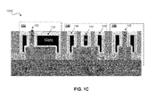
- FIGs. 1A through1C illustrate cross-sectional and top views of examples of a lateral double-diffused MOS (LDMOS) bulk finFET device for high-voltage operation in accordance with one or more implementations.
- An LDMOS bulk finFET device (hereinafter "LDMOS device"), as shown in the cross-sectional view 100A, includes a first-well region 110 and two or more second-well regions, for example, 120-1 and 120-2 formed on a substrate material 105.
- the LDMOS device further includes one or more non-well regions, such as the non-well region 115.
- the non-well regions include the same material as the substrate material 105, whereas the first-well region and the second-well regions include doped semiconductor material (e.g., silicon).
- the non-well regions e.g., 115
- separate well regions e.g., 120-1 and 120-2) of the second-well regions.
- the LDMOS device is an NLDMOS device formed on a substrate material (e.g., 105) consisting p-type silicon.
- the first-well region 110 is a p-well region doped with p-type impurity
- the second-well regions e.g., 120-1 and 120-2 are n-well regions doped with n-type impurity for the charge carriers, which are electrons, to pass through.
- the region 115 can be a p-well region separating the n-well regions.
- the LDMOS device can be a PLDMOS device fabricated on a substrate material consisting of deep n-well in silicon.
- the first-well region 110 can be an n-well region
- the second-well regions e.g., 120-1 and 120-2
- the region 115 can be an n-well, a deep n-well, or a combination of the n-well and the deep n-well.
- a source structure 130 is disposed on a first fin 135 that is partially formed on the first-well region 110.
- a drain structure 150 is disposed on a second fin 155 that is formed on a last one of second-well regions (e.g., 120-2).
- One or more dummy regions e.g., 140
- the dummy regions 140 can provide additional depletion region flow paths including vertical flow paths for charge carriers to enable the high-voltage operation.
- the high voltage operation of the LDMOS device depends, among other things, on the path length of the charge carriers (e.g., electrons) through the depletion regions.
- the depletion regions would be formed only in the first well region 110 (e.g., p-well) and the second well region(s) 120 (e.g., n-well(s)), which would not be separated by the non-well region 115.
- the subject technology provides the additional depletion regions in the dummy region 140, which makes the charge carriers to pass through a lengthier path 160, than if the dummy region 140 did not exist (e.g., the existing technology).
- the additional depletion regions are formed at the junction of the non-well region 115 (e.g., p-type) and a dummy fin145 (n-type) formed in the dummy region 140.
- the additional depletion regions extend both horizontally (e.g., along the top portion of the dummy fin 145) and vertically (e.g., along the side portions of the dummy fin 145) to increase the length of the path 160 of the charge carriers (e.g., electrons) in the depletion regions.
- the increased path length of the charge carriers in the additional depletion regions leads to higher device breakdown voltage (e.g., between a source 132 and a drain 152 of the LDMOS device).
- the source structure 130 includes a source 132 built on the top of an epitaxial formation 138 covering a portion of the first fin 135, a dummy gate structure 136, and a gate structure 134.
- the gate structure 134 covers a portion of the first fin 135 including an edge of the first fin 135.
- the drain structure 150 includes a drain 152 built on top of an epitaxial formation 158 covering a portion of the second fin 155 and dummy gate structures 154 and 156.
- the dummy gate structures 136 of the source structure 130 and dummy gate structures 154 and 156 of the drain structure 150 have no functionality related to the subject technology, and are shown as they are part of the normal finFET-based CMOS fabrication process flow.
- FIG. 1B illustrates a top view 100B of the LDMOS device of FIG. 1A .
- the top view 100B shows regions 160, 170, and 180, respectively corresponding to the source structure 130, the dummy region 140, and drain structure 150 of the cross-sectional view 100A.
- a broken line A-A' shows an axis, across which the cross-sectional view 100A is shown.
- the region 160 shows a number of (e.g., three) first fins 135, portions of which are covered with the epitaxial formations 138 and the gate structure 134.
- the region 170 depicts a number of (e.g., three) dummy fins 145, and the region 180 shows a number of (e.g., three) second fins 155, partially covered with the epitaxial formations 158.
- each of the dummy regions includes a dummy gate 142, dummy epitaxial formations 148, and dummy gate structures 144 and 146, disposed on the dummy fin 145.
- the LDMOS device shown in the cross-section view 100C is otherwise similar to the LDMOS device shown in the cross-section view 100A. It is understood that the high-voltage operation of the LDMOS device is achievable without these dummy structures including the dummy gate 142, the dummy epitaxial formations 148, and the dummy gate structures 144 and 146. These dummy structures are not essential to the operation of the subject technology and are added to conform to finFET-based CMOS fabrication process flow.
- the dummy gate 142 although not essential, but when coupled to a suitable bias voltage, does not interfere with the high voltage operation of the device, as discussed below. It is important to note that the LDMOS device of the subject technology can be fabricated using normal finFET-based CMOS device fabrication process flow without additional masks or process steps, thus with no additional cost.
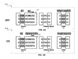
- FIGs. 2A and 2B illustrate examples of high-voltage operation modes 200A and 200B of the LDMOS device of FIG. 1A in accordance with one or more implementations.
- the source 132 and the gate 134 are connected to a lowest voltage (e.g., zero voltage such as ground potential) and the drain 152 is connected to a high voltage (e.g., 5V).
- the source 132 is connected to the lowest voltage (e.g., zero voltage such as ground potential) and the drain 152 is connected to a high voltage (e.g., 5V), while the gate 134 is connected to suitable gate voltage (e.g., 1.8V) above the threshold voltage of the LDMOS device.
- the dummy region 140 of the LDMOS device of FIGs. 2A and 2B has no dummy gates, therefore the dummy region 140 is not expected to interfere with the high-voltage operation of the LDMOS device.
- FIGs. 3A and 3B illustrate examples of high-voltage operation modes 300A and 300B of the LDMOS device of FIG. 1C in accordance with one or more implementations.
- the source 132 and the gate 134 are connected to a lowest voltage (e.g., zero voltage such as ground potential) and the drain 152 is connected to a high voltage (e.g., 5V).
- the dummy region 140 as shown in FIG. 1C , includes the dummy gate 142, which, for the proper operation of the LDMOS device, is connected to a suitable voltage (e.g., 1.8 V) above the threshold voltage of the LDMOS device
- the source 132 is connected to the lowest voltage (e.g., zero voltage such as ground potential) and the drain 152 is connected to a high voltage (e.g., 5V), while the gate 134 and the dummy gate 142 of FIG.1C are connected to suitable gate voltage (e.g., 1.8V) above the threshold voltage of the LDMOS device.
- the lowest voltage e.g., zero voltage such as ground potential
- the drain 152 is connected to a high voltage (e.g., 5V)
- suitable gate voltage e.g., 1.8V
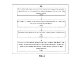
- FIG. 4 illustrates an example of a method 400 for forming an LDMOS device for high-voltage operation in accordance with one or more implementations.
- the example method 400 is described herein with reference to, but is not limited to, the process disclosed with respect the LDMOS device of FIG. 1A .
- the blocks of the example method 400 are described herein as occurring in serial, or linearly. However, multiple blocks of the example method 400 can occur in parallel.
- the blocks of the example method 400 need not be performed in the order shown and/or one or more of the blocks of the example method 400 need not be performed.
- the method 400 includes forming a first-well region (e.g., 110 of FIG. 1A ) and two or more second-well regions (e.g., 120-1 and 120-2 of FIG. 1A ) on a substrate material (e.g., 105 of FIG. 1A ) (410).
- the two or more second-well regions are separated by one or more non-well regions (e.g., 115 of FIG. 1A ).
- a first fin e.g., 135 of FIG. 1A
- a second fin e.g., 155 of FIG. 1A
- a source structure (e.g., 130 of FIG. 1A ) is disposed on the first fin and a drain structure (e.g., 150 of FIG. 1A ) on the second fin (430).
- One or more dummy regions (e.g., 140 of FIG. 1A ) are formed on the one or more non-well regions (440).
- the dummy regions provide additional depletion region flow paths (e.g., portions of path 160, which is in the dummy region 140 of FIG. 1A ) including vertical flow paths for charge carriers to enable the high-voltage operation.
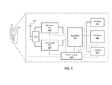
- FIG. 5 illustrates an example of a wireless communication device in accordance with one or more implementations.
- the wireless communication device 500 includes a radio-frequency (RF) antenna 510, a receiver 520, a transmitter 530, a baseband processing module 540, a memory 550, a processor 460, a local oscillator generator (LOGEN) 570, and a power supply 580.
- RF radio-frequency
- LOGEN local oscillator generator
- one or more of the blocks represented in FIG. 5 can be integrated on one or more semiconductor substrates.
- the blocks 520-570 can be realized in a single chip or a single system on chip, or can be realized in a multi-chip chipset.
- the RF antenna 510 can be suitable for transmitting and/or receiving RF signals (e.g., wireless signals) over a wide range of frequencies. Although a single RF antenna 510 is illustrated, the subject technology is not so limited.
- the receiver 520 comprises suitable logic circuitry and/or code that can be operable to receive and process signals from the RF antenna 510.
- the receiver 520 may, for example, be operable to amplify and/or down-convert received wireless signals.
- the receiver 520 is operable to cancel noise in received signals and can be linear over a wide range of frequencies. In this manner, the receiver 520 is suitable for receiving signals in accordance with a variety of wireless standards. Wi-Fi, WiMAX, Bluetooth, and various cellular standards.
- the transmitter 530 comprises suitable logic circuitry and/or code that can be operable to process and transmit signals from the RF antenna 510.
- the transmitter 530 may, for example, be operable to up-convert baseband signals to RF signals and amplify RF signals.
- the transmitter 530 is operable to up-convert and to amplify baseband signals processed in accordance with a variety of wireless standards. Examples of such standards include Wi-Fi, WiMAX, Bluetooth, and various cellular standards.
- the transmitter 530 is operable to provide signals for further amplification by one or more power amplifiers.
- the transmitter 530 includes an RF power amplifier that can be a high-voltage power amplifier fabricated using the LDMOS device (e.g. as shown in FIGs. 1A or 1C ) of the subject technology.
- the duplexer 512 provides isolation in the transmit band to avoid saturation of the receiver 520 or damaging parts of the receiver 520, and to relax one or more design requirements of the receiver 520. Furthermore, the duplexer 512 can attenuate the noise in the receive band.
- the duplexer is operable in multiple frequency bands of various wireless standards.
- the baseband processing module 540 comprises suitable logic, circuitry, interfaces, and/or code that can be operable to perform processing of baseband signals.
- the baseband processing module 540 may, for example, analyze received signals and generate control and/or feedback signals for configuring various components of the wireless communication device 500 such as the receiver 520.
- the baseband processing module 540 is operable to encode, decode, transcode, modulate, demodulate, encrypt, decrypt, scramble, descramble, and/or otherwise process data in accordance with one or more wireless standards.
- the processor 560 comprises suitable logic, circuitry, and/or code that can enable processing data and/or controlling operations of the wireless communication device 500.
- the processor 560 is enabled to provide control signals to various other portions of the wireless communication device 500.
- the processor 560 can also control transfers of data between various portions of the wireless communication device 500.
- the processor 560 can enable implementation of an operating system or otherwise execute code to manage operations of the wireless communication device 500.
- the memory 550 comprises suitable logic, circuitry, and/or code that can enable storage of various types of information such as received data, generated data, code, and/or configuration information.
- the local oscillator generator (LOG EN) 570 comprises suitable logic, circuitry, interfaces, and/or code that can be operable to generate one or more oscillating signals of one or more frequencies.
- the LOGEN 570 can be operable to generate digital and/or analog signals. In this manner, the LOGEN 570 can be operable to generate one or more clock signals and/or sinusoidal signals. Characteristics of the oscillating signals such as the frequency and duty cycle can be determined based on one or more control signals from, for example, the processor 560 and/or the baseband processing module 540.
- the processor 560 can configure the various components of the wireless communication device 500 based on a wireless standard according to which it is desired to receive signals.
- Wireless signals can be received via the RF antenna 510 and amplified and down-converted by the receiver 520.
- the baseband processing module 540 can perform noise estimation and/or noise cancellation, decoding, and/or demodulation of the baseband signals. In this manner, information in the received signal can be recovered and utilized appropriately.
- the information can be audio and/or video to be presented to a user of the wireless communication device, data to be stored to the memory 550, and/or information affecting and/or enabling operation of the wireless communication device 500.
- the baseband processing module 540 can modulate, encode and perform other processing on audio, video, and/or control signals to be transmitted by the transmitter 530 in accordance to various wireless standards.
- the phrase "at least one of” preceding a series of items, with the term “and” or “or” to separate any of the items, modifies the list as a whole, rather than each member of the list (i.e., each item).
- the phrase "at least one of” does not require selection of at least one of each item listed; rather, the phrase allows a meaning that includes at least one of any one of the items, and/or at least one of any combination of the items, and/or at least one of each of the items.
- phrases “at least one of A, B, and C” or “at least one of A, B, or C” each refer to only A, only B, or only C; any combination of A, B, and C; and/or at least one of each of A, B, and C.
- a phrase such as "an aspect” does not imply that such aspect is essential to the subject technology or that such aspect applies to all configurations of the subject technology.
- a disclosure relating to an aspect can apply to all configurations, or one or more configurations.
- An aspect can provide one or more examples of the disclosure.
- a phrase such as an "aspect” refers to one or more aspects and vice versa.
- a phrase such as an "embodiment” does not imply that such embodiment is essential to the subject technology or that such embodiment applies to all configurations of the subject technology.
- a disclosure relating to an embodiment can apply to all embodiments, or one or more embodiments.
- An embodiment can provide one or more examples of the disclosure.
- a phrase such an "embodiment” can refer to one or more embodiments and vice versa.
- a phrase such as a "configuration” does not imply that such configuration is essential to the subject technology or that such configuration applies to all configurations of the subject technology.
- a disclosure relating to a configuration can apply to all configurations, or one or more configurations.
- a configuration can provide one or more examples of the disclosure.
- a phrase such as a "configuration” can refer to one or more configurations and vice versa.
Landscapes
- Metal-Oxide And Bipolar Metal-Oxide Semiconductor Integrated Circuits (AREA)
- Insulated Gate Type Field-Effect Transistor (AREA)
Abstract
Description
- The present disclosure relates generally to integrated circuits, and more particularly, but not exclusively, to a lateral double-diffused MOS (LDMOS) device and structure for bulk fin field-effect transistor (finFET) technology.
- There are a number of challenges that scaling of conventional planar metal-oxide-semiconductor field-effect transistors (MOSFETs) are faced with. For example, threshold swing degradation, large drain-induced barrier lowering (DIBL), device characteristics fluctuations, and leakage are among the most common problems that may be addressed by 3-D device structures. Fin field-effect transistors (FinFETs) are 3-D device structures that can be used in nano-scale complementary metal-oxide-semiconductor (CMOS) and high-density memory applications.
- FinFET devices are divided into two categories, bulk finFETs and silicon-on-insulator (SOI) finFETs. In bulk finFET devices, which are more common in 14nm and/or 16nm technology, the fin can be formed on the bulk silicon (e.g., silicon substrate). The bulk finFET can be produced at low cost, low defect density, high heat transfer to substrate, and good process control. Bulk finFETs with lateral double-diffused MOS (LDMOS) structures, which are mostly used in RF power amplifiers, can provide a high breakdown voltage (e.g., between drain and source terminals). The high breakdown voltage is achieved, for example, by a charge carrier (e.g., electron) flow path that passes through a depletion region.
- In accordance with a first aspect of the present disclosure, there is provided a lateral double-diffused MOS (LDMOS) bulk finFET device for high-voltage operation, the device comprising:
- a first-well region and two or more second-well regions formed on a substrate material and one or more non-well regions comprising substrate material, wherein the one or more non-well regions are configured to separate well regions of the two or more second-well regions;
- a source structure disposed on a first fin partially formed on the first-well region;
- a drain structure disposed on a second fin formed on a last one of the two or more second-well regions; and
- one or more dummy regions formed on the one or more non-well regions, wherein the dummy regions are configured to provide additional depletion region flow paths including vertical flow paths for charge carriers to enable the high-voltage operation.
- In accordance with a second aspect of the present disclosure, there is provided a method for forming a lateral double-diffused MOS (LDMOS) bulk finFET device for high-voltage operation, the method comprising:
- forming a first-well region and two or more second-well regions on a substrate material, wherein the two or more second-well regions are separated by one or more non-well regions;
- forming a first fin partially on the first-well region and a second fin on a last one of the two or more second-well regions;
- disposing a source structure on the first fin and a drain structure on the second fin; and
- forming one or more dummy regions on the one or more non-well regions, wherein the dummy regions are configured to provide additional depletion region flow paths including vertical flow paths for charge carriers to enable the high-voltage operation.
- In accordance with a third aspect of the present disclosure, there is provided a communication device, comprising:
- a transmitter circuit including a radio-frequency (RF) power amplifier, wherein the RF power amplifier is fabricated using lateral double-diffused MOS (LDMOS) bulk finFET devices for high-voltage operation, each LDMOS bulk finFET device comprising:
- a first-well region and two or more second-well regions formed on a substrate material and one or more non-well regions comprising substrate material, wherein the one or more non-well regions are configured to separate well regions of the two or more second-well regions;
- a source structure disposed on a first fin partially formed on the first-well region;
- a drain structure disposed on a second fin formed on a last one of the two or more second-well regions; and
- one or more dummy regions formed on the one or more non-well regions, wherein the dummy regions are configured to provide additional depletion region flow paths including vertical flow paths for charge carriers to enable the high-voltage operation.
- Further features and advantages will become apparent from the following description of embodiments of the present disclosure, given by way of example only, which is made with reference to the accompanying drawings.
- Certain features of the subject technology are set forth in the appended claims. However, for purpose of explanation, several embodiments of the subject technology are set forth in the following figures.
-
FIGs. 1A through 1C illustrate cross-sectional and top views of examples of a lateral double-diffused MOS (LDMOS) bulk finFET device for high-voltage operation in accordance with one or more implementations. -
FIGs. 2A and 2B illustrate examples of high-voltage operation modes of the LDMOS bulk finFET device ofFIG. 1A in accordance with one or more implementations. -
FIGs. 3A and 3B illustrate examples of high-voltage operation modes of an LDMOS bulk finFET device ofFIG. 1C in accordance with one or more implementations. -
FIG. 4 illustrates an example of a method for forming an LDMOS bulk finFET device for high-voltage operation in accordance with one or more implementations. -
FIG. 5 illustrates an example of a wireless communication device in accordance with one or more implementations. - The detailed description set forth below is intended as a description of various configurations of the subject technology and is not intended to represent the only configurations in which the subject technology can be practiced. The appended drawings are incorporated herein and constitute a part of the detailed description. The detailed description includes specific details for the purpose of providing a thorough understanding of the subject technology. However, it will be clear and apparent to those skilled in the art that the subject technology is not limited to the specific details set forth herein and can be practiced using one or more implementations. In one or more instances, well-known structures and components are shown in block diagram form in order to avoid obscuring the concepts of the subject technology.
- The subject technology may provide methods and implementations for providing bulk finFET devices with lateral double-diffused MOS (LDMOS) structures for high-voltage operations. In one or more implementations, the subject technology achieves higher breakdown voltage by increasing the flow path of the charge carriers (e.g., electrons in NLDMOS or holes in PLDMOS) in one or more additional depletion regions. The advantageous features of the disclosed solution include compatibility with the existing finFET-based CMOS device fabrication process flow without requiring any additional masks.
-
FIGs. 1A through1C illustrate cross-sectional and top views of examples of a lateral double-diffused MOS (LDMOS) bulk finFET device for high-voltage operation in accordance with one or more implementations. An LDMOS bulk finFET device (hereinafter "LDMOS device"), as shown in thecross-sectional view 100A, includes a first-well region 110 and two or more second-well regions, for example, 120-1 and 120-2 formed on a substrate material 105. The LDMOS device further includes one or more non-well regions, such as the non-well region 115. The non-well regions (e.g., 115) include the same material as the substrate material 105, whereas the first-well region and the second-well regions include doped semiconductor material (e.g., silicon). The non-well regions (e.g., 115) separate well regions (e.g., 120-1 and 120-2) of the second-well regions. - In one or more implementations, the LDMOS device, as shown in
FIG. 1A , is an NLDMOS device formed on a substrate material (e.g., 105) consisting p-type silicon. In this case, the first-well region 110 is a p-well region doped with p-type impurity, and the second-well regions (e.g., 120-1 and 120-2) are n-well regions doped with n-type impurity for the charge carriers, which are electrons, to pass through. In some implementations, the region 115 can be a p-well region separating the n-well regions. - In some aspects, the LDMOS device can be a PLDMOS device fabricated on a substrate material consisting of deep n-well in silicon. The first-
well region 110 can be an n-well region, and the second-well regions (e.g., 120-1 and 120-2) can be p-well regions for the charge carriers (e.g., holes) to travel through. In some aspects, for the PLDMOS device, the region 115 can be an n-well, a deep n-well, or a combination of the n-well and the deep n-well. - A
source structure 130 is disposed on a first fin 135 that is partially formed on the first-well region 110. Adrain structure 150 is disposed on asecond fin 155 that is formed on a last one of second-well regions (e.g., 120-2). One or more dummy regions (e.g., 140) are formed on the one or more non-well regions (e.g., 115). Thedummy regions 140 can provide additional depletion region flow paths including vertical flow paths for charge carriers to enable the high-voltage operation. The high voltage operation of the LDMOS device depends, among other things, on the path length of the charge carriers (e.g., electrons) through the depletion regions. Without the dummy region(s) of the subject technology, the depletion regions would be formed only in the first well region 110 (e.g., p-well) and the second well region(s) 120 (e.g., n-well(s)), which would not be separated by the non-well region 115. The subject technology provides the additional depletion regions in thedummy region 140, which makes the charge carriers to pass through alengthier path 160, than if thedummy region 140 did not exist (e.g., the existing technology). The additional depletion regions are formed at the junction of the non-well region 115 (e.g., p-type) and a dummy fin145 (n-type) formed in thedummy region 140. The additional depletion regions extend both horizontally (e.g., along the top portion of the dummy fin 145) and vertically (e.g., along the side portions of the dummy fin 145) to increase the length of thepath 160 of the charge carriers (e.g., electrons) in the depletion regions. The increased path length of the charge carriers in the additional depletion regions leads to higher device breakdown voltage (e.g., between asource 132 and adrain 152 of the LDMOS device). - The
source structure 130 includes asource 132 built on the top of anepitaxial formation 138 covering a portion of the first fin 135, adummy gate structure 136, and agate structure 134. Thegate structure 134 covers a portion of the first fin 135 including an edge of the first fin 135. Thedrain structure 150 includes adrain 152 built on top of anepitaxial formation 158 covering a portion of thesecond fin 155 anddummy gate structures dummy gate structures 136 of thesource structure 130 anddummy gate structures drain structure 150 have no functionality related to the subject technology, and are shown as they are part of the normal finFET-based CMOS fabrication process flow. -
FIG. 1B illustrates atop view 100B of the LDMOS device ofFIG. 1A . Thetop view 100B showsregions source structure 130, thedummy region 140, anddrain structure 150 of thecross-sectional view 100A. A broken line A-A' shows an axis, across which thecross-sectional view 100A is shown. Theregion 160 shows a number of (e.g., three) first fins 135, portions of which are covered with theepitaxial formations 138 and thegate structure 134. Theregion 170 depicts a number of (e.g., three)dummy fins 145, and theregion 180 shows a number of (e.g., three)second fins 155, partially covered with theepitaxial formations 158. - In one or more implementations, as shown in the
cross-sectional view 100C ofFIG. 1C , each of the dummy regions (e.g., 140) includes adummy gate 142, dummyepitaxial formations 148, anddummy gate structures dummy fin 145. The LDMOS device shown in thecross-section view 100C is otherwise similar to the LDMOS device shown in thecross-section view 100A. It is understood that the high-voltage operation of the LDMOS device is achievable without these dummy structures including thedummy gate 142, the dummyepitaxial formations 148, and thedummy gate structures - The
dummy gate 142, although not essential, but when coupled to a suitable bias voltage, does not interfere with the high voltage operation of the device, as discussed below. It is important to note that the LDMOS device of the subject technology can be fabricated using normal finFET-based CMOS device fabrication process flow without additional masks or process steps, thus with no additional cost. -
FIGs. 2A and 2B illustrate examples of high-voltage operation modes FIG. 1A in accordance with one or more implementations. In the off mode of the LDMOS device, as shown in theoperation mode 200A, thesource 132 and thegate 134 are connected to a lowest voltage (e.g., zero voltage such as ground potential) and thedrain 152 is connected to a high voltage (e.g., 5V). - In the on mode of the LDMOS device, as shown in the
operation mode 200B, thesource 132 is connected to the lowest voltage (e.g., zero voltage such as ground potential) and thedrain 152 is connected to a high voltage (e.g., 5V), while thegate 134 is connected to suitable gate voltage (e.g., 1.8V) above the threshold voltage of the LDMOS device. Thedummy region 140 of the LDMOS device ofFIGs. 2A and 2B has no dummy gates, therefore thedummy region 140 is not expected to interfere with the high-voltage operation of the LDMOS device. -
FIGs. 3A and 3B illustrate examples of high-voltage operation modes 300A and 300B of the LDMOS device ofFIG. 1C in accordance with one or more implementations. In the off mode of the LDMOS device, as shown in theoperation mode 300A, thesource 132 and thegate 134 are connected to a lowest voltage (e.g., zero voltage such as ground potential) and thedrain 152 is connected to a high voltage (e.g., 5V). Thedummy region 140, as shown inFIG. 1C , includes thedummy gate 142, which, for the proper operation of the LDMOS device, is connected to a suitable voltage (e.g., 1.8 V) above the threshold voltage of the LDMOS device - In the on mode of the LDMOS device, as shown in the operation mode 300B, the
source 132 is connected to the lowest voltage (e.g., zero voltage such as ground potential) and thedrain 152 is connected to a high voltage (e.g., 5V), while thegate 134 and thedummy gate 142 ofFIG.1C are connected to suitable gate voltage (e.g., 1.8V) above the threshold voltage of the LDMOS device. -
FIG. 4 illustrates an example of amethod 400 for forming an LDMOS device for high-voltage operation in accordance with one or more implementations. For explanatory purposes, theexample method 400 is described herein with reference to, but is not limited to, the process disclosed with respect the LDMOS device ofFIG. 1A . Further, for explanatory purposes, the blocks of theexample method 400 are described herein as occurring in serial, or linearly. However, multiple blocks of theexample method 400 can occur in parallel. In addition, the blocks of theexample method 400 need not be performed in the order shown and/or one or more of the blocks of theexample method 400 need not be performed. - The
method 400 includes forming a first-well region (e.g., 110 ofFIG. 1A ) and two or more second-well regions (e.g., 120-1 and 120-2 ofFIG. 1A ) on a substrate material (e.g., 105 ofFIG. 1A ) (410). The two or more second-well regions are separated by one or more non-well regions (e.g., 115 ofFIG. 1A ). A first fin (e.g., 135 ofFIG. 1A ) is formed partially on the first-well region and a second fin (e.g., 155 ofFIG. 1A ) is formed on a last one of the two or more second-well regions (e.g., 120-2 ofFIG. 1A ) (420). A source structure (e.g., 130 ofFIG. 1A ) is disposed on the first fin and a drain structure (e.g., 150 ofFIG. 1A ) on the second fin (430). One or more dummy regions (e.g., 140 ofFIG. 1A ) are formed on the one or more non-well regions (440). The dummy regions provide additional depletion region flow paths (e.g., portions ofpath 160, which is in thedummy region 140 ofFIG. 1A ) including vertical flow paths for charge carriers to enable the high-voltage operation. -
FIG. 5 illustrates an example of a wireless communication device in accordance with one or more implementations. Thewireless communication device 500 includes a radio-frequency (RF)antenna 510, areceiver 520, atransmitter 530, abaseband processing module 540, amemory 550, a processor 460, a local oscillator generator (LOGEN) 570, and apower supply 580. In various embodiments of the subject technology, one or more of the blocks represented inFIG. 5 can be integrated on one or more semiconductor substrates. For example, the blocks 520-570 can be realized in a single chip or a single system on chip, or can be realized in a multi-chip chipset. - The
RF antenna 510 can be suitable for transmitting and/or receiving RF signals (e.g., wireless signals) over a wide range of frequencies. Although asingle RF antenna 510 is illustrated, the subject technology is not so limited. - The
receiver 520 comprises suitable logic circuitry and/or code that can be operable to receive and process signals from theRF antenna 510. Thereceiver 520 may, for example, be operable to amplify and/or down-convert received wireless signals. In various embodiments of the subject technology, thereceiver 520 is operable to cancel noise in received signals and can be linear over a wide range of frequencies. In this manner, thereceiver 520 is suitable for receiving signals in accordance with a variety of wireless standards. Wi-Fi, WiMAX, Bluetooth, and various cellular standards. - The
transmitter 530 comprises suitable logic circuitry and/or code that can be operable to process and transmit signals from theRF antenna 510. Thetransmitter 530 may, for example, be operable to up-convert baseband signals to RF signals and amplify RF signals. In various embodiments of the subject technology, thetransmitter 530 is operable to up-convert and to amplify baseband signals processed in accordance with a variety of wireless standards. Examples of such standards include Wi-Fi, WiMAX, Bluetooth, and various cellular standards. In various embodiments of the subject technology, thetransmitter 530 is operable to provide signals for further amplification by one or more power amplifiers. - In some implementations, the
transmitter 530 includes an RF power amplifier that can be a high-voltage power amplifier fabricated using the LDMOS device (e.g. as shown inFIGs. 1A or1C ) of the subject technology. - The
duplexer 512 provides isolation in the transmit band to avoid saturation of thereceiver 520 or damaging parts of thereceiver 520, and to relax one or more design requirements of thereceiver 520. Furthermore, theduplexer 512 can attenuate the noise in the receive band. The duplexer is operable in multiple frequency bands of various wireless standards. - The
baseband processing module 540 comprises suitable logic, circuitry, interfaces, and/or code that can be operable to perform processing of baseband signals. Thebaseband processing module 540 may, for example, analyze received signals and generate control and/or feedback signals for configuring various components of thewireless communication device 500 such as thereceiver 520. Thebaseband processing module 540 is operable to encode, decode, transcode, modulate, demodulate, encrypt, decrypt, scramble, descramble, and/or otherwise process data in accordance with one or more wireless standards. - The
processor 560 comprises suitable logic, circuitry, and/or code that can enable processing data and/or controlling operations of thewireless communication device 500. In this regard, theprocessor 560 is enabled to provide control signals to various other portions of thewireless communication device 500. Theprocessor 560 can also control transfers of data between various portions of thewireless communication device 500. Additionally, theprocessor 560 can enable implementation of an operating system or otherwise execute code to manage operations of thewireless communication device 500. - The
memory 550 comprises suitable logic, circuitry, and/or code that can enable storage of various types of information such as received data, generated data, code, and/or configuration information. The local oscillator generator (LOG EN) 570 comprises suitable logic, circuitry, interfaces, and/or code that can be operable to generate one or more oscillating signals of one or more frequencies. TheLOGEN 570 can be operable to generate digital and/or analog signals. In this manner, theLOGEN 570 can be operable to generate one or more clock signals and/or sinusoidal signals. Characteristics of the oscillating signals such as the frequency and duty cycle can be determined based on one or more control signals from, for example, theprocessor 560 and/or thebaseband processing module 540. - In operation, the
processor 560 can configure the various components of thewireless communication device 500 based on a wireless standard according to which it is desired to receive signals. Wireless signals can be received via theRF antenna 510 and amplified and down-converted by thereceiver 520. Thebaseband processing module 540 can perform noise estimation and/or noise cancellation, decoding, and/or demodulation of the baseband signals. In this manner, information in the received signal can be recovered and utilized appropriately. For example, the information can be audio and/or video to be presented to a user of the wireless communication device, data to be stored to thememory 550, and/or information affecting and/or enabling operation of thewireless communication device 500. Thebaseband processing module 540 can modulate, encode and perform other processing on audio, video, and/or control signals to be transmitted by thetransmitter 530 in accordance to various wireless standards. - Those of skill in the art would appreciate that the various illustrative blocks, modules, elements, components, and methods described herein can be implemented as electronic hardware, computer software, or combinations of both. To illustrate this interchangeability of hardware and software, various illustrative blocks, modules, elements, components, and methods have been described above generally in terms of their functionality. Whether such functionality is implemented as hardware or software depends upon the particular application and design constraints imposed on the overall system. Skilled artisans can implement the described functionality in varying ways for each particular application. Various components and blocks can be arranged differently (e.g., arranged in a different order, or partitioned in a different way) all without departing from the scope of the subject technology.
- As used herein, the phrase "at least one of" preceding a series of items, with the term "and" or "or" to separate any of the items, modifies the list as a whole, rather than each member of the list (i.e., each item). The phrase "at least one of" does not require selection of at least one of each item listed; rather, the phrase allows a meaning that includes at least one of any one of the items, and/or at least one of any combination of the items, and/or at least one of each of the items. By way of example, the phrases "at least one of A, B, and C" or "at least one of A, B, or C" each refer to only A, only B, or only C; any combination of A, B, and C; and/or at least one of each of A, B, and C.
- A phrase such as "an aspect" does not imply that such aspect is essential to the subject technology or that such aspect applies to all configurations of the subject technology. A disclosure relating to an aspect can apply to all configurations, or one or more configurations. An aspect can provide one or more examples of the disclosure. A phrase such as an "aspect" refers to one or more aspects and vice versa. A phrase such as an "embodiment" does not imply that such embodiment is essential to the subject technology or that such embodiment applies to all configurations of the subject technology. A disclosure relating to an embodiment can apply to all embodiments, or one or more embodiments. An embodiment can provide one or more examples of the disclosure. A phrase such an "embodiment" can refer to one or more embodiments and vice versa. A phrase such as a "configuration" does not imply that such configuration is essential to the subject technology or that such configuration applies to all configurations of the subject technology. A disclosure relating to a configuration can apply to all configurations, or one or more configurations. A configuration can provide one or more examples of the disclosure. A phrase such as a "configuration" can refer to one or more configurations and vice versa.
- The word "exemplary" is used herein to mean "serving as an example, instance, or illustration." Any embodiment described herein as "exemplary" or as an "example" is not necessarily to be construed as preferred or advantageous over other embodiments. Furthermore, to the extent that the term "include," "have," or the like is used in the description or the claims, such term is intended to be inclusive in a manner similar to the term "comprise" as "comprise" is interpreted when employed as a transitional word in a claim.
- All structural and functional equivalents to the elements of the various aspects described throughout this disclosure that are known or later come to be known to those of ordinary skill in the art are expressly incorporated herein by reference and are intended to be encompassed by the claims. Moreover, nothing disclosed herein is intended to be dedicated to the public regardless of whether such disclosure is explicitly recited in the claims. No claim element is to be construed under the provisions of 35 U.S.C. §112, sixth paragraph, unless the element is expressly recited using the phrase "means for" or, in the case of a method claim, the element is recited using the phrase "step for."
- The previous description is provided to enable any person skilled in the art to practice the various aspects described herein. Various modifications to these aspects will be readily apparent to those skilled in the art, and the generic principles defined herein can be applied to other aspects. Thus, the claims are not intended to be limited to the aspects shown herein, but are to be accorded the full scope consistent with the language claims, wherein reference to an element in the singular is not intended to mean "one and only one" unless specifically so stated, but rather "one or more." Unless specifically stated otherwise, the term "some" refers to one or more. Pronouns in the masculine (e.g., his) include the feminine and neuter gender (e.g., her and its) and vice versa. Headings and subheadings, if any, are used for convenience only and do not limit the subject disclosure.
- The above embodiments are to be understood as illustrative examples of the present disclosure. Further embodiments of the present disclosure are envisaged. It is to be understood that any feature described in relation to any one embodiment may be used alone, or in combination with other features described, and may also be used in combination with one or more features of any other of the embodiments, or any combination of any other of the embodiments. Furthermore, equivalents and modifications not described above may also be employed without departing from the scope of embodiments, which is defined in the accompanying claims.
Claims (15)
- A lateral double-diffused MOS (LDMOS) bulk finFET device for high-voltage operation, the device comprising:a first-well region and two or more second-well regions formed on a substrate material and one or more non-well regions comprising substrate material, wherein the one or more non-well regions are configured to separate well regions of the two or more second-well regions;a source structure disposed on a first fin partially formed on the first-well region;a drain structure disposed on a second fin formed on a last one of the two or more second-well regions; andone or more dummy regions formed on the one or more non-well regions, wherein the dummy regions are configured to provide additional depletion region flow paths including vertical flow paths for charge carriers to enable the high-voltage operation.
- A device according to claim 1, wherein the LDMOS bulk finFET device comprises an NLDMOS bulk finFET device, the substrate material comprises p-type silicon, the first-well region comprises a p-well region, the two or more second-well regions comprise n-well regions, and the charge carriers comprise electrons.
- A device according to claim 1, wherein the LDMOS bulk finFET device comprises a PLDMOS bulk finFET device, the substrate material comprises a deep n-well in silicon, the first-well region comprises an n-well region, the two or more second-well regions comprise p-well regions, and the charge carriers comprise holes.
- A device according to any preceding claim, wherein each of the one or more dummy regions comprises a dummy fin formed on one of the one or more non-well regions, wherein each of the one or more dummy regions are configurable to allow the vertical flow paths for charge carriers to pass through the dummy fin.
- A device according to claim 4, wherein each of the one or more dummy regions comprises a dummy gate disposed on the dummy fin to conform to finFET-based CMOS fabrication process flow, wherein the high-voltage operation of the device is achievable without the dummy gate, and wherein the dummy gate is configured to allow the high voltage operation of the device, when coupled to a suitable bias voltage.
- A method for forming a lateral double-diffused MOS (LDMOS) bulk finFET device for high-voltage operation, the method comprising:forming a first-well region and two or more second-well regions on a substrate material, wherein the two or more second-well regions are separated by one or more non-well regions;forming a first fin partially on the first-well region and a second fin on a last one of the two or more second-well regions;disposing a source structure on the first fin and a drain structure on the second fin; andforming one or more dummy regions on the one or more non-well regions, wherein the dummy regions are configured to provide additional depletion region flow paths including vertical flow paths for charge carriers to enable the high-voltage operation.
- A method according to claim 6, wherein forming the LDMOS bulk finFET device comprises forming an NLDMOS bulk finFET device, the substrate material comprises p-type silicon, the first-well region comprises a p-well region, forming the two or more second-well regions comprises forming n-well regions, and the charge carriers comprise electrons.
- A method according to claim 6, wherein forming the LDMOS bulk finFET device comprises forming a PLDMOS bulk finFET device, the substrate material comprises a deep n-well in silicon, forming the first-well region comprises forming an n-well region, forming the two or more second-well regions comprises forming p-well regions, and the charge carriers comprise holes.
- A method according to any of claims 6 to 8, wherein each of the one or more dummy regions comprises a dummy fin formed on one of the one or more non-well regions, and wherein each of the one or more dummy regions are configurable to allow the vertical flow paths for charge carriers to pass through the dummy fin.
- A method according to claim 9, wherein forming each of the one or more dummy regions comprises disposing a dummy gate on the dummy fin to conform to finFET-based CMOS fabrication process flow, wherein the high-voltage operation of the device is achievable without the dummy gate.
- A method according to any of claims 6 to 10, further comprising:configuring the dummy gate to allow the high voltage operation of the device, when coupled to a suitable bias voltage; andfabricating the LDMOS bulk finFET using finFET-based CMOS fabrication process flow without additional masks or process steps.
- A communication device, comprising:a transmitter circuit including a radio-frequency (RF) power amplifier, wherein the RF power amplifier is fabricated using lateral double-diffused MOS (LDMOS) bulk finFET devices for high-voltage operation, each LDMOS bulk finFET device comprising:a first-well region and two or more second-well regions formed on a substrate material and one or more non-well regions comprising substrate material, wherein the one or more non-well regions are configured to separate well regions of the two or more second-well regions;a source structure disposed on a first fin partially formed on the first-well region;a drain structure disposed on a second fin formed on a last one of the two or more second-well regions; andone or more dummy regions formed on the one or more non-well regions, wherein the dummy regions are configured to provide additional depletion region flow paths including vertical flow paths for charge carriers to enable the high-voltage operation.
- A communication device according to claim 12, wherein each of the one or more dummy regions comprises a dummy fin formed on one of the one or more non-well regions, and wherein each of the one or more dummy regions are configurable to allow the vertical flow paths for charge carriers to pass through the dummy fin.
- A communication device according to claim 12, wherein each of the one or more dummy regions comprises a dummy gate disposed on the dummy fin to conform to finFET-based CMOS fabrication process flow, wherein the high-voltage operation of the device is achievable without the dummy gate.
- A communication device according to claim 14, wherein the dummy gate is configured to allow the high voltage operation of the device, when coupled to a suitable bias voltage, and wherein the LDMOS bulk finFET device is fabricated using finFET-based CMOS fabrication process flow without additional masks or process steps.
Applications Claiming Priority (2)
| Application Number | Priority Date | Filing Date | Title |
|---|---|---|---|
| US201462007832P | 2014-06-04 | 2014-06-04 | |
| US14/309,843 US9379236B2 (en) | 2014-06-04 | 2014-06-19 | LDMOS device and structure for bulk FinFET technology |
Publications (1)
| Publication Number | Publication Date |
|---|---|
| EP2953168A1 true EP2953168A1 (en) | 2015-12-09 |
Family
ID=53267250
Family Applications (1)
| Application Number | Title | Priority Date | Filing Date |
|---|---|---|---|
| EP15169215.9A Withdrawn EP2953168A1 (en) | 2014-06-04 | 2015-05-26 | Device and structure for bulk finfet technology |
Country Status (4)
| Country | Link |
|---|---|
| US (1) | US9379236B2 (en) |
| EP (1) | EP2953168A1 (en) |
| CN (2) | CN204792801U (en) |
| HK (1) | HK1215895A1 (en) |
Cited By (2)
| Publication number | Priority date | Publication date | Assignee | Title |
|---|---|---|---|---|
| EP3188248A1 (en) * | 2015-12-30 | 2017-07-05 | IMEC vzw | High voltage tolerant ldmos |
| EP3258498A1 (en) * | 2016-06-15 | 2017-12-20 | Semiconductor Manufacturing International Corporation (Shanghai) | Ldmos design for a finfet device |
Families Citing this family (22)
| Publication number | Priority date | Publication date | Assignee | Title |
|---|---|---|---|---|
| US9379236B2 (en) * | 2014-06-04 | 2016-06-28 | Broadcom Corporation | LDMOS device and structure for bulk FinFET technology |
| US9653466B2 (en) * | 2015-08-04 | 2017-05-16 | Qualcomm Incorporated | FinFET device and method of making the same |
| CN105428353B (en) * | 2015-12-17 | 2018-08-21 | 江南大学 | A kind of high-voltage ESD protective device with class fin LDMOS structure |
| KR102421730B1 (en) | 2016-04-05 | 2022-07-18 | 삼성전자주식회사 | Layout method and semiconductor device |
| CN107452729B (en) * | 2016-06-01 | 2020-09-15 | 中芯国际集成电路制造(上海)有限公司 | Electrostatic discharge ESD protection devices and semiconductor devices |
| CN107516668B (en) | 2016-06-15 | 2020-04-24 | 中芯国际集成电路制造(北京)有限公司 | Semiconductor device and method for manufacturing the same |
| US20170365675A1 (en) * | 2016-06-16 | 2017-12-21 | United Microelectronics Corp. | Dummy pattern arrangement and method of arranging dummy patterns |
| CN107634056B (en) | 2016-07-07 | 2021-06-29 | 联华电子股份有限公司 | Semiconductor device and method of forming the same |
| CN107644815B (en) * | 2016-07-21 | 2021-04-23 | 中芯国际集成电路制造(上海)有限公司 | Semiconductor device, manufacturing method thereof and electronic device |
| TWI698021B (en) | 2016-09-13 | 2020-07-01 | 聯華電子股份有限公司 | Semiconductor device and method for fabricating the same |
| CN108155111B (en) * | 2016-12-02 | 2020-05-08 | 中芯国际集成电路制造(上海)有限公司 | Semiconductor test structure and forming method thereof |
| US10396159B2 (en) * | 2017-10-30 | 2019-08-27 | Avago Technologies International Sales Pte. Limited | FinFET cascode laterally-diffused semiconductor device |
| US9992496B1 (en) * | 2017-11-15 | 2018-06-05 | Google Llc | Bin string coding based on a most probable symbol |
| US10600866B2 (en) * | 2018-02-01 | 2020-03-24 | Qualcomm Incorporated | Standard cell architecture for gate tie-off |
| US10741685B2 (en) | 2018-09-21 | 2020-08-11 | Globalfoundries Inc. | Semiconductor devices having a fin channel arranged between source and drift regions and methods of manufacturing the same |
| US11075298B2 (en) | 2019-06-27 | 2021-07-27 | Globalfoundries U.S. Inc. | LDMOS integrated circuit product |
| US11195947B2 (en) | 2019-10-24 | 2021-12-07 | Globalfoundries U.S. Inc. | Semiconductor device with doped region adjacent isolation structure in extension region |
| US11183591B2 (en) | 2019-10-30 | 2021-11-23 | Avago Technologies International Sales Pte. Ltd. | Lateral double-diffused metal-oxide-semiconductor (LDMOS) fin field effect transistor with enhanced capabilities |
| US12218134B2 (en) * | 2021-01-22 | 2025-02-04 | Taiwan Semiconductor Manufacturing Co., Ltd. | Semiconductor device and method |
| CN116031299B (en) | 2021-10-26 | 2026-02-24 | 联华电子股份有限公司 | Lateral diffusion metal oxide semiconductor element |
| US20250040256A1 (en) * | 2023-07-24 | 2025-01-30 | Avago Technologies International Sales Pte. Limited | Semiconductor device with electrostatic discharge protection |
| TWI887076B (en) * | 2024-08-09 | 2025-06-11 | 聯華電子股份有限公司 | Semiconductor device and method for fabricating the same |
Citations (6)
| Publication number | Priority date | Publication date | Assignee | Title |
|---|---|---|---|---|
| JP2007059427A (en) * | 2005-08-22 | 2007-03-08 | Seiko Epson Corp | Semiconductor device and manufacturing method thereof, MIS type high voltage transistor |
| US20110215423A1 (en) * | 2010-03-05 | 2011-09-08 | Renesas Electronics Corporation | Semiconductor device and a manufacturing method thereof |
| US20120049279A1 (en) * | 2010-08-25 | 2012-03-01 | Mayank Shrivastava | High Voltage Semiconductor Devices |
| US20130292777A1 (en) * | 2012-05-03 | 2013-11-07 | Taiwan Semiconductor Manufacturing Company, Ltd. | Structure for FinFETs |
| US20140008733A1 (en) * | 2012-07-03 | 2014-01-09 | Intel Mobile Communications GmbH | Drain extended mos device for bulk finfet technology |
| US8716791B1 (en) * | 2011-08-11 | 2014-05-06 | Maxim Integrated Products, Inc. | LDMOS with corrugated drift region |
Family Cites Families (11)
| Publication number | Priority date | Publication date | Assignee | Title |
|---|---|---|---|---|
| US8004038B2 (en) * | 2006-05-22 | 2011-08-23 | Taiwan Semiconductor Manufacturing Company, Ltd. | Suppression of hot-carrier effects using double well for thin gate oxide LDMOS embedded in HV process |
| KR20100064556A (en) * | 2008-12-05 | 2010-06-15 | 주식회사 동부하이텍 | A semiconductor device and method of manufacturing the same |
| TWI455316B (en) * | 2011-01-28 | 2014-10-01 | 立錡科技股份有限公司 | High voltage multi-gate element and method of manufacturing same |
| US9647066B2 (en) * | 2012-04-24 | 2017-05-09 | Taiwan Semiconductor Manufacturing Company, Ltd. | Dummy FinFET structure and method of making same |
| US20140167173A1 (en) * | 2012-12-14 | 2014-06-19 | Broadcom Corporation | Increasing the breakdown voltage of a metal oxide semiconductor device |
| US9306057B2 (en) * | 2012-12-27 | 2016-04-05 | Broadcom Corporation | Metal oxide semiconductor devices and fabrication methods |
| US9105719B2 (en) * | 2013-01-09 | 2015-08-11 | Broadcom Corporation | Multigate metal oxide semiconductor devices and fabrication methods |
| US9041127B2 (en) * | 2013-05-14 | 2015-05-26 | International Business Machines Corporation | FinFET device technology with LDMOS structures for high voltage operations |
| US9418993B2 (en) * | 2013-08-05 | 2016-08-16 | Globalfoundries Inc. | Device and method for a LDMOS design for a FinFET integrated circuit |
| US9379236B2 (en) * | 2014-06-04 | 2016-06-28 | Broadcom Corporation | LDMOS device and structure for bulk FinFET technology |
| US9082852B1 (en) * | 2014-12-04 | 2015-07-14 | Stmicroelectronics, Inc. | LDMOS FinFET device using a long channel region and method of manufacture |
-
2014
- 2014-06-19 US US14/309,843 patent/US9379236B2/en active Active
-
2015
- 2015-05-26 EP EP15169215.9A patent/EP2953168A1/en not_active Withdrawn
- 2015-06-03 CN CN201520379079.3U patent/CN204792801U/en not_active Withdrawn - After Issue
- 2015-06-03 CN CN201510301027.9A patent/CN105322017B/en active Active
-
2016
- 2016-04-05 HK HK16103791.7A patent/HK1215895A1/en unknown
Patent Citations (6)
| Publication number | Priority date | Publication date | Assignee | Title |
|---|---|---|---|---|
| JP2007059427A (en) * | 2005-08-22 | 2007-03-08 | Seiko Epson Corp | Semiconductor device and manufacturing method thereof, MIS type high voltage transistor |
| US20110215423A1 (en) * | 2010-03-05 | 2011-09-08 | Renesas Electronics Corporation | Semiconductor device and a manufacturing method thereof |
| US20120049279A1 (en) * | 2010-08-25 | 2012-03-01 | Mayank Shrivastava | High Voltage Semiconductor Devices |
| US8716791B1 (en) * | 2011-08-11 | 2014-05-06 | Maxim Integrated Products, Inc. | LDMOS with corrugated drift region |
| US20130292777A1 (en) * | 2012-05-03 | 2013-11-07 | Taiwan Semiconductor Manufacturing Company, Ltd. | Structure for FinFETs |
| US20140008733A1 (en) * | 2012-07-03 | 2014-01-09 | Intel Mobile Communications GmbH | Drain extended mos device for bulk finfet technology |
Cited By (4)
| Publication number | Priority date | Publication date | Assignee | Title |
|---|---|---|---|---|
| EP3188248A1 (en) * | 2015-12-30 | 2017-07-05 | IMEC vzw | High voltage tolerant ldmos |
| US10680098B2 (en) | 2015-12-30 | 2020-06-09 | Imec Vzw | High voltage tolerant LDMOS |
| EP3258498A1 (en) * | 2016-06-15 | 2017-12-20 | Semiconductor Manufacturing International Corporation (Shanghai) | Ldmos design for a finfet device |
| US10043804B2 (en) | 2016-06-15 | 2018-08-07 | Semiconductor Manufacturing International (Shanghai) Corporation | LDMOS design for a FinFET device |
Also Published As
| Publication number | Publication date |
|---|---|
| CN105322017A (en) | 2016-02-10 |
| HK1215895A1 (en) | 2016-09-23 |
| US9379236B2 (en) | 2016-06-28 |
| US20150357462A1 (en) | 2015-12-10 |
| CN204792801U (en) | 2015-11-18 |
| CN105322017B (en) | 2019-03-19 |
Similar Documents
| Publication | Publication Date | Title |
|---|---|---|
| US9379236B2 (en) | LDMOS device and structure for bulk FinFET technology | |
| US10505020B2 (en) | FinFET LDMOS devices with improved reliability | |
| US9209202B2 (en) | Enabling bulk FINFET-based devices for FINFET technology with dielectric isolation | |
| US9543383B2 (en) | High-speed high-power semiconductor devices | |
| EP2894668B1 (en) | Dummy end-gate based anti-fuse device for finFET technologies | |
| CN109728094B (en) | FINFET cascode laterally diffused semiconductor device | |
| US10483960B2 (en) | Radio frequency switch with low oxide stress | |
| KR20140001145A (en) | Body-contacted partially depleted silicon on insulator transistor | |
| JP2015149720A (en) | Field effect transistor switch circuit | |
| US10157907B2 (en) | Semiconductor device and method of manufacturing the same | |
| US12598800B2 (en) | Wide bandgap transistor layout with staggered gate electrode fingers and split active regions | |
| US10340289B2 (en) | Cascode radio frequency (RF) power amplifier on single diffusion | |
| US20160149033A1 (en) | Increasing breakdown voltage of ldmos devices for foundry processes | |
| US9520398B1 (en) | Including low and high-voltage CMOS devices in CMOS process | |
| US9379212B1 (en) | Extended-drain transistor using inner spacer | |
| US12224347B2 (en) | P-type field effect transistor (PFET) on a silicon germanium (Ge) buffer layer to increase Ge in the PFET source and drain to increase compression of the PFET channel and method of fabrication | |
| WO2026084825A1 (en) | Asymmetric pmos fets |
Legal Events
| Date | Code | Title | Description |
|---|---|---|---|
| PUAI | Public reference made under article 153(3) epc to a published international application that has entered the european phase |
Free format text: ORIGINAL CODE: 0009012 |
|
| AK | Designated contracting states |
Kind code of ref document: A1 Designated state(s): AL AT BE BG CH CY CZ DE DK EE ES FI FR GB GR HR HU IE IS IT LI LT LU LV MC MK MT NL NO PL PT RO RS SE SI SK SM TR |
|
| AX | Request for extension of the european patent |
Extension state: BA ME |
|
| 17P | Request for examination filed |
Effective date: 20160609 |
|
| RBV | Designated contracting states (corrected) |
Designated state(s): AL AT BE BG CH CY CZ DE DK EE ES FI FR GB GR HR HU IE IS IT LI LT LU LV MC MK MT NL NO PL PT RO RS SE SI SK SM TR |
|
| RAP1 | Party data changed (applicant data changed or rights of an application transferred) |
Owner name: AVAGO TECHNOLOGIES GENERAL IP (SINGAPORE) PTE. LTD |
|
| RAP1 | Party data changed (applicant data changed or rights of an application transferred) |
Owner name: AVAGO TECHNOLOGIES INTERNATIONAL SALES PTE. LIMITE |
|
| STAA | Information on the status of an ep patent application or granted ep patent |
Free format text: STATUS: EXAMINATION IS IN PROGRESS |
|
| 17Q | First examination report despatched |
Effective date: 20190711 |
|
| STAA | Information on the status of an ep patent application or granted ep patent |
Free format text: STATUS: THE APPLICATION IS DEEMED TO BE WITHDRAWN |
|
| 18D | Application deemed to be withdrawn |
Effective date: 20211201 |