EP2953154A1 - Usage of Si-O-Si based molecules for high efficiency Si solar cells - Google Patents
Usage of Si-O-Si based molecules for high efficiency Si solar cells Download PDFInfo
- Publication number
- EP2953154A1 EP2953154A1 EP14305829.5A EP14305829A EP2953154A1 EP 2953154 A1 EP2953154 A1 EP 2953154A1 EP 14305829 A EP14305829 A EP 14305829A EP 2953154 A1 EP2953154 A1 EP 2953154A1
- Authority
- EP
- European Patent Office
- Prior art keywords
- silicon oxide
- deposition
- doping source
- layers
- siox
- Prior art date
- Legal status (The legal status is an assumption and is not a legal conclusion. Google has not performed a legal analysis and makes no representation as to the accuracy of the status listed.)
- Withdrawn
Links
Images


Classifications
-
- H—ELECTRICITY
- H01—ELECTRIC ELEMENTS
- H01L—SEMICONDUCTOR DEVICES NOT COVERED BY CLASS H10
- H01L21/00—Processes or apparatus adapted for the manufacture or treatment of semiconductor or solid state devices or of parts thereof
- H01L21/02—Manufacture or treatment of semiconductor devices or of parts thereof
- H01L21/02104—Forming layers
- H01L21/02107—Forming insulating materials on a substrate
- H01L21/02109—Forming insulating materials on a substrate characterised by the type of layer, e.g. type of material, porous/non-porous, pre-cursors, mixtures or laminates
- H01L21/02112—Forming insulating materials on a substrate characterised by the type of layer, e.g. type of material, porous/non-porous, pre-cursors, mixtures or laminates characterised by the material of the layer
- H01L21/02123—Forming insulating materials on a substrate characterised by the type of layer, e.g. type of material, porous/non-porous, pre-cursors, mixtures or laminates characterised by the material of the layer the material containing silicon
- H01L21/02126—Forming insulating materials on a substrate characterised by the type of layer, e.g. type of material, porous/non-porous, pre-cursors, mixtures or laminates characterised by the material of the layer the material containing silicon the material containing Si, O, and at least one of H, N, C, F, or other non-metal elements, e.g. SiOC, SiOC:H or SiONC
- H01L21/02129—Forming insulating materials on a substrate characterised by the type of layer, e.g. type of material, porous/non-porous, pre-cursors, mixtures or laminates characterised by the material of the layer the material containing silicon the material containing Si, O, and at least one of H, N, C, F, or other non-metal elements, e.g. SiOC, SiOC:H or SiONC the material being boron or phosphorus doped silicon oxides, e.g. BPSG, BSG or PSG
Definitions
- the invention concerns the use of Si-O-Si based molecules for the deposition of undoped and doped microcrystalline silicon oxide ( ⁇ c-SiOx:H) films on a substrate surface (silicon wafers, glass, metals).
- ⁇ c-SiOx:H microcrystalline silicon oxide
- the doped ⁇ c-SiOx:H can be used as a p type layer or a n type layer in single junction and multi-junction silicon thin film solar cells or as the Silicon Oxide Intermediate Reflector (SOIR) in multi-junction silicon thin film solar cells.
- Undoped and doped hydrogenated microcrystalline silicon oxide ( ⁇ c-SiOx:H) thin films have attracted particular scientific interest due to their potential applications in single and multi-junction thin film solar cells.
- the most widely used method for producing the material is Plasma Enhanced Chemical Vapor Deposition (PECVD) method from highly diluted SiH 4 in H 2 discharges with water, oxygen, N 2 O or most often carbon dioxide gas as an oxygen source.
- PECVD Plasma Enhanced Chemical Vapor Deposition
- the doping is done using B 2 H 6 , Trimethylborane (TMB) as 'p' type dopant and PH 3 as 'n' type dopant.
- These p and n type doped layers can be used as p and n type layers in single junction and multi-junction amorphous layers.
- the doped ⁇ c-SiOx:H can also be used as Silicon Oxide Intermediate Reflector (SOIR) in multi-junction solar cells.
- ⁇ c-SiOx:H films consist of a mixed phase material based on an oxygen rich amorphous silicon oxide and a doped microcrystalline silicon phase.
- the properties of the films varies. With an increase in the oxidant content, more oxygen is incorporated in the films and the material gets a reduced refractive index (compared to Si) but the electrical conductivity decreases and the structure of the material changes from highly crystalline to fully amorphous.
- microcrystalline silicon oxide ( ⁇ c-SiOx:H) film on a substrate surface with superior qualities, notably conductivity and transparency with better control of film properties during the deposition processes and thus resulting in thin film Si solar cells with improved efficiencies.
- an object of the present invention is a method for deposing on a substrate a microcrystalline silicon oxide layer of formula SiO x :H, where 0 ⁇ x ⁇ 2, comprising introducing into a deposition zone where the substrate is located a gas mixture comprising :
- the invention concerns:
- the silicon oxide layer is a p-type layer and the doping source comprises at least one atom of Bore.
- the silicon oxide layer is a p-type layer and the doping source is diborane.
- the silicon oxide layer is a n-type layer and the doping source comprises at least one atom of Phosphorus.
- the silicon oxide layer is a n-type layer and the doping source is phosphine.
- the silicon precursor is hexamethyldisiloxane (HMDSO) or tetramethyldisiloxane (TMDSO).
- HMDSO hexamethyldisiloxane
- TMDSO tetramethyldisiloxane
- step (ii) comprised, for 100% in volume, between 0.2% and 1% of monosilane.
- Si-O-Si based molecules according to the invention there is one Oxygen atom and two Silicon atoms. This results in a better control of the properties of the deposited films and serves as an extra source of Silicon which leads to the formation of denser Silicon thin films. These enhanced properties enable to achieve high efficiency thin film solar cells and one needs to explore this subject further and invoke the use of advanced Si-O-Si based molecules during the deposition of ⁇ c-SiOx:H films.
- Si-O-Si based molecules have been used for depositing microcrystalline silicon oxide ( ⁇ c-SiOx:H) film on a substrate surface with superior qualities, notably conductivity and transparency.
- Molecules like HMDSO and TMDSO are being used for the depositions. These molecules give better control of film properties during the deposition processes and thus result in thin film Si solar cells with improved efficiencies.
- These molecules are used for the deposition of high quality undoped and doped microcrystalline silicon oxide ( ⁇ c-SiOx:H) film on a substrate surface.
- Si-O-Si molecules present advantages over the conventional water, oxygen, N 2 O or CO 2 as source of oxygen atom in the deposition of intrinsic and doped microcrystalline silicon oxide ( ⁇ c-SiOx:H) film on a substrate surface in the following ways:
- a preferred method for deposition of hydrogenated microcrystalline silicon oxide thin films is as following:
- Example 1 Hydrogenated micro-crystalline silicon oxide films
- ⁇ c-SiOx:H is obtained by implementing a gas mixture comprising of monosilane, hydrogenand Si-O-Si based molecules according to the invention under CVD conditions.
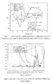
- Figure 1 compares the ellipsometry spectra obtained through the depositions with HMDSO with the undoped and 'p' type doped ⁇ c-SiOx:H films. As seen in Figure 1 , the intensity of ellipsometry spectra from the 'p' type ⁇ c-SiOx:H films obtained from HMDSO as the oxygen source decreases as HMDSO flow rate increases. This indicates that the Oxygen content in the films is increasing.
- Figure 2 compares the FTIR spectra of the depositions in different gas mixture conditions.
- the FTIR spectra of the p type ⁇ c-Si:H films, p type ⁇ c-SiOx:H films from CO 2 and p type ⁇ c-SiOx:H films from HMDSO is shown.
- the presence of a peak ( ⁇ 1200 cm -1 ) in FTIR spectra indicates the presence of Si-O. This peak is seen in the FTIR spectra of SiO 2 films, p- ⁇ c-SiOx:H from CO 2 as Oxygen source and p- ⁇ c-SiOx:H from HMDSO as the Oxygen source.
- the described Si-O-Si molecules of the invention presents a new method to deposit undoped and doped microcrystalline silicon oxide ( ⁇ c-SiOx:H) film on a substrate surface.
- ⁇ c-SiOx:H microcrystalline silicon oxide
- These films have superior properties (refractive index, optical band gap, conductivity, mechanical and material) than the conventional films deposited from other oxygen sources like water, oxygen, N 2 O and CO 2 . These enhanced properties will facilitate the increased efficiencies of the solar cells.
- Example 2 - p-type microcrystalline silicon oxide layers using HMDSO as the Oxygen source.
- the doped layers (p-type and n-type) in thin film silicon solar cells are necessary to provide an electron-hole separation mechanism. These layers are a source of parasitic absorption, but can provide an advantage if they provide greater control over optical reflection.
- Doped microcrystalline silicon oxide ( ⁇ c-SiOx:H) is a material which has gained scientific interest because of its reduced optical absorption while still generating sufficient electric field for electron-hole separation.
- Hexamethyldisiloxane C 6 H 18 OSi 2 , HMDSO
- HMDSO Hexamethyldisiloxane
- the use of molecules with pre-formed Si-O-Si bonds as the oxygen source growth precursor is expected to provide different material properties ascompared to when the Oxygen arrives as either an atom or as a hydroxyl group (-OH).
- CO 2 is used as the Oxygen source for depositing p-type ⁇ c-SiOx:H layers.
- p- ⁇ c-SiOx:H layers were deposited on glass substrate (AF-32) and FZ Wafer.
- the refractive index (n) of the layers was estimated by fitting the Ellipsometry curves on Delta-Psi2 software.
- the coplanar conductivities were evaluated by evaporating metal contacts on the deposited layers and measuring the current at a specified voltage.
- the bond configuration in the films was confirmed with Fourier Transform Infrared Spectroscopy (FTIR).
- FTIR Fourier Transform Infrared Spectroscopy
- SIMS Secondary Ion Mass Spectroscopy
- the p-type layers from HMDSO were also tested in a single junction amorphous silicon p-i-n type device structures which demonstrated the functioning of the new p-type layers in the devices.
- Figure 3 shows the comparison of Refractive Index (n) of the layers as a function of Oxygen source/SiH 4 flow.
- the Oxygen source is HMDSO in one case and CO 2 in another case.
- Figure 4 shows the comparison of coplanar conductivities of the layers as a function of Oxygen source/SiH 4 flow.
- FTIR Fourier Transform Infrared Spectroscopy
- Figure 5 shows the FTIR Spectra of the p- ⁇ c-SiOx:H layers deposited with HMDSO.
- the C density is ⁇ 10 22 at/cm 3 while in the standard p- ⁇ c-SiOx:H layers, it is about ⁇ 10 21 at/cm 3 .
- HMDSO has six CH 3 groups.
- the other elements (B, Si, H, O) have almost similar densities.
Abstract
- a silicon precursor of (R1R2R3)Si-O-Si(R4R5R6) where R1-R6 are organic ligands independently selected from the group consisting of H, C1-C5 linear or branched, alkyl, aryl, alkenyl ; and
- monosilane, hydrogen and a doping source.
Description
- The invention concerns the use of Si-O-Si based molecules for the deposition of undoped and doped microcrystalline silicon oxide (µc-SiOx:H) films on a substrate surface (silicon wafers, glass, metals). The doped µc-SiOx:H can be used as a p type layer or a n type layer in single junction and multi-junction silicon thin film solar cells or as the Silicon Oxide Intermediate Reflector (SOIR) in multi-junction silicon thin film solar cells.
- Undoped and doped hydrogenated microcrystalline silicon oxide (µc-SiOx:H) thin films have attracted particular scientific interest due to their potential applications in single and multi-junction thin film solar cells. The most widely used method for producing the material is Plasma Enhanced Chemical Vapor Deposition (PECVD) method from highly diluted SiH4 in H2 discharges with water, oxygen, N2O or most often carbon dioxide gas as an oxygen source. The doping is done using B2H6, Trimethylborane (TMB) as 'p' type dopant and PH3 as 'n' type dopant.
- These p and n type doped layers can be used as p and n type layers in single junction and multi-junction amorphous layers. The doped µc-SiOx:H can also be used as Silicon Oxide Intermediate Reflector (SOIR) in multi-junction solar cells.
- µc-SiOx:H films consist of a mixed phase material based on an oxygen rich amorphous silicon oxide and a doped microcrystalline silicon phase. Depending on the nature of the oxidant gas and their ratios, the properties of the films varies. With an increase in the oxidant content, more oxygen is incorporated in the films and the material gets a reduced refractive index (compared to Si) but the electrical conductivity decreases and the structure of the material changes from highly crystalline to fully amorphous.
- The domain of the properties (refractive index, optical band gap, conductivity, mechanical and material) which can be explored when using water, oxygen, N2O or CO2 as the O source in µc-SiOx:H is limited.
- The presence of doped layers is necessary for the fabrication of thin-film silicon solar cells, but these layers also give parasitic absorption, decreasing cell efficiency. Consequently there is a need for depositing microcrystalline silicon oxide (µc-SiOx:H) film on a substrate surface with superior qualities, notably conductivity and transparency with better control of film properties during the deposition processes and thus resulting in thin film Si solar cells with improved efficiencies.
- Consequently, an object of the present invention is a method for deposing on a substrate a microcrystalline silicon oxide layer of formula SiOx:H, where 0 < x < 2, comprising introducing into a deposition zone where the substrate is located a gas mixture comprising :
- a silicon precursor of (R1R2R3)Si-O-Si(R4R5R6) where R1-R6 are organic ligands independently selected from the group consisting of H, C1-C5 linear or branched, alkyl, aryl, alkenyl ; and
- monosilane, hydrogen and a doping source.
- According to other embodiments, the invention concerns:
- A method as defined above, wherein the silicon oxide layer is a p-type layer and the doping source comprises at least one atom of Bore.
- A method as defined above, wherein the silicon oxide layer is a p-type layer and the doping source is diborane.
- A method as defined above, wherein the silicon oxide layer is a n-type layer and the doping source comprises at least one atom of Phosphorus.
- A method as defined above, wherein the silicon oxide layer is a n-type layer and the doping source is phosphine.
- A method as defined above, wherein the silicon precursor is hexamethyldisiloxane (HMDSO) or tetramethyldisiloxane (TMDSO).
- A method as defined above, wherein the deposition is performed by chemical vapour deposition and comprises at least one cycle comprising the following steps:
- (i) introducing the silicon precursor into a deposition zone where the substrate is located; and
- (ii) introducing the gas mixture of monosilane, hydrogen and a doping source into the deposition zone.
- A method as defined above, wherein the steps are performed simultaneously.
- A method as defined above, wherein the steps are performed sequentially.
- A method as defined above, wherein the temperature maintained in the deposition zone is comprised between 150°C and 250°C and the pressure maintained in the deposition zone is comprised between 133 Pa and 333 Pa.
- A method as defined above, wherein the gas mixture introduced at step (ii) comprised, for 100% in volume, between 0.2% and 1% of monosilane.
- A method as defined above, wherein the silicon precursor is added to the gas mixture in a range comprised, in volume, between 10% and 100% of the monosilane.
- In Si-O-Si based molecules according to the invention, there is one Oxygen atom and two Silicon atoms. This results in a better control of the properties of the deposited films and serves as an extra source of Silicon which leads to the formation of denser Silicon thin films. These enhanced properties enable to achieve high efficiency thin film solar cells and one needs to explore this subject further and invoke the use of advanced Si-O-Si based molecules during the deposition of µc-SiOx:H films.
- Si-O-Si based molecules have been used for depositing microcrystalline silicon oxide (µc-SiOx:H) film on a substrate surface with superior qualities, notably conductivity and transparency. Molecules like HMDSO and TMDSO are being used for the depositions. These molecules give better control of film properties during the deposition processes and thus result in thin film Si solar cells with improved efficiencies.
- These molecules are used for the deposition of high quality undoped and doped microcrystalline silicon oxide (µc-SiOx:H) film on a substrate surface.
- These Si-O-Si molecules present advantages over the conventional water, oxygen, N2O or CO2 as source of oxygen atom in the deposition of intrinsic and doped microcrystalline silicon oxide (µc-SiOx:H) film on a substrate surface in the following ways:
- 1. Si-O-Si based molecules according to the invention have only one Oxygen atom and two Silicon atoms. During the deposition in a CVD system, the oxidation of microcrystalline Silicon will be limited and two additional Silicon atoms will result in the deposition of denser intrinsic and doped microcrystalline silicon oxide (µc-SiOx:H) film.
- 2. These Si-O-Si based molecules according to the invention, have sufficient volatility for vapour phase distribution and can be distributed easily using a conventional liquid molecule distribution system.
- Those skilled in the art will recognise that these molecules can also be used for various other applications like deposition of SiOC films which have a higher band gap and can be used in the doped layers of a thin film Si Solar cell.
- A preferred method for deposition of hydrogenated microcrystalline silicon oxide thin films is as following:
- 1. A mixture of 0.2% to 1 % silane is used in hydrogen.
- 2. The flow rate of SiH4 ranges from 0 to 10 sccm.
- 3. The power densities can be ranged from 0 to 800 mW/cm2.
- 4. Si-O-Si based molecule (HMDSO, TMDSO,...) is added to the mixture and it ranges from 10% to 100% of the SiH4.
- 5. The applied pressure was between 133 Pa to 333 Pa.
- 6. The temperature of the substrate ranges from 150°C to 250°C.
- µc-SiOx:H is obtained by implementing a gas mixture comprising of monosilane, hydrogenand Si-O-Si based molecules according to the invention under CVD conditions.
Figure 1 compares the ellipsometry spectra obtained through the depositions with HMDSO with the undoped and 'p' type doped µc-SiOx:H films. As seen inFigure 1 , the intensity of ellipsometry spectra from the 'p' type µc-SiOx:H films obtained from HMDSO as the oxygen source decreases as HMDSO flow rate increases. This indicates that the Oxygen content in the films is increasing. -
Figure 2 compares the FTIR spectra of the depositions in different gas mixture conditions. The FTIR spectra of the p type µc-Si:H films, p type µc-SiOx:H films from CO2 and p type µc-SiOx:H films from HMDSO is shown. The presence of a peak (∼1200 cm-1) in FTIR spectra indicates the presence of Si-O. This peak is seen in the FTIR spectra of SiO2 films, p-µc-SiOx:H from CO2 as Oxygen source and p-µc-SiOx:H from HMDSO as the Oxygen source. - The described Si-O-Si molecules of the invention presents a new method to deposit undoped and doped microcrystalline silicon oxide (µc-SiOx:H) film on a substrate surface. These films have superior properties (refractive index, optical band gap, conductivity, mechanical and material) than the conventional films deposited from other oxygen sources like water, oxygen, N2O and CO2. These enhanced properties will facilitate the increased efficiencies of the solar cells.
- The doped layers (p-type and n-type) in thin film silicon solar cells are necessary to provide an electron-hole separation mechanism. These layers are a source of parasitic absorption, but can provide an advantage if they provide greater control over optical reflection.
- Doped microcrystalline silicon oxide (µc-SiOx:H) is a material which has gained scientific interest because of its reduced optical absorption while still generating sufficient electric field for electron-hole separation.
- In this example, the use of Hexamethyldisiloxane (C6H18OSi2, HMDSO) as an oxygen source for microcrystalline silicon oxide p-type layers deposited by PECVD is illustrated. The use of molecules with pre-formed Si-O-Si bonds as the oxygen source growth precursor is expected to provide different material properties ascompared to when the Oxygen arrives as either an atom or as a hydroxyl group (-OH). Conventionally, CO2 is used as the Oxygen source for depositing p-type µc-SiOx:H layers.
- p-µc-SiOx:H layers were deposited on glass substrate (AF-32) and FZ Wafer. The refractive index (n) of the layers was estimated by fitting the Ellipsometry curves on Delta-Psi2 software. The coplanar conductivities were evaluated by evaporating metal contacts on the deposited layers and measuring the current at a specified voltage. The bond configuration in the films was confirmed with Fourier Transform Infrared Spectroscopy (FTIR). The elemental composition and density of the elements in the deposited films was checked with Secondary Ion Mass Spectroscopy (SIMS) analysis. All the properties of the films were compared with the p-µc-SiOx:H layers using CO2 as Oxygen source.
- The p-type layers from HMDSO were also tested in a single junction amorphous silicon p-i-n type device structures which demonstrated the functioning of the new p-type layers in the devices.
-
Figure 3 shows the comparison of Refractive Index (n) of the layers as a function of Oxygen source/SiH4 flow. The Oxygen source is HMDSO in one case and CO2 in another case. - As seen in
Figure 3 , with HMDSO, layers were obtained in the range of n ∼3.5 to 2.2 while with CO2, n changed drastically (2.3 to 1.7) with a slight increase in CO2 flow. -
Figure 4 shows the comparison of coplanar conductivities of the layers as a function of Oxygen source/SiH4 flow. - As seen in
Figure 4 , it was easier to control the conductivities between 10-4 S/cm and 10-10 S/cm with HMDSO compared to CO2. These layers are interesting for p-type layer in a single junction cell and as an Intermediate Reflector Layer (IRL) in a micromorph cell. -
Figure 5 shows the FTIR Spectra of the p-µc-SiOx:H layers deposited with HMDSO. - As seen in
Figure 5 , there is a peak at 1100 cm-1 which indicates Si-O bond in the deposited films. This peak is typically seen in the FTIR spectra of the µc-SiOx:H layers. - The p-type layers from HMDSO were deposited on FZ Crystalline Wafer substrate and SIMS analysis were performed to know the elemental composition and the density.
Figure 6 shows the elements and their densities in p-µc-SiOx:H layers from HMDSO. - As seen in
Figure 6 , the C density is ∼1022 at/cm3 while in the standard p-µc-SiOx:H layers, it is about ∼1021at/cm3. This is expected because HMDSO has six CH3 groups. The other elements (B, Si, H, O) have almost similar densities. - The p-type layers from HMDSO were also tested in a single junction silicon p-i-n type device structures.
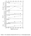
Figure 7 shows the cell parameters as a function of HMDSO flow whileFigure 8 shows the External Quantum Efficiency (EQE). - The p-type layers were tested in a single junction silicon p-i-n type device structures, and the following best cell parameters (Jsc= 11.4 mA/cm2, Voc= 0.81 V, FF= 60, η = 5.5 %) were obtained using very thick p-layers and aluminium back reflectors. Further, annealing of the cells led to a small increase in Voc, but the main limitation (low current) is expected to be overcome using thinner p-layers and an improved back reflector.
Claims (12)
- A method for deposing on a substrate a microcrystalline silicon oxide layer of formula SiOx:H, where 0 < x < 2, comprising introducing into a deposition zone where the substrate is located a gas mixture comprising :- a silicon precursor of (R1R2R3)Si-O-Si(R4R5R6) where R1-R6 are organic ligands independently selected from the group consisting of H, C1-C5 linear or branched, alkyl, aryl, alkenyl ; and- monosilane, hydrogen and a doping source.
- A method according to Claim 1, wherein the silicon oxide layer is a p-type layer and the doping source comprises at least one atom of Bore.
- A method according to Claim 2, wherein the silicon oxide layer is a p-type layer and the doping source is diborane.
- A method according to Claim 1, wherein the silicon oxide layer is a n-type layer and the doping source comprises at least one atom of Phosphorus.
- A method according to Claim 4, wherein the silicon oxide layer is a n-type layer and the doping source is phosphine.
- A method according to anyone of claims 1 to 5 wherein the silicon precursor is hexamethyldisiloxane (HMDSO) or tetramethyldisiloxane (TMDSO).
- A method according to anyone of claims 1 to 6 wherein the deposition is performed by chemical vapour deposition and comprises at least one cycle comprising the following steps:(i) introducing the silicon precursor into a deposition zone where the substrate is located; and(ii) introducing the gas mixture of monosilane, hydrogen and a doping source into the deposition zone.
- A method according to Claim 7, wherein the steps are performed simultaneously.
- A method according to Claim 7, wherein the steps are performed sequentially.
- A method according to anyone of preceding claims, wherein the temperature maintained in the deposition zone is comprised between 150°C and 250°C and the pressure maintained in the deposition zone is comprised between 133 Pa and 333 Pa.
- A method according to anyone of claims 7 to 10, wherein the gas mixture introduced at step (ii) comprised, for 100% in volume, between 0.2% and 1% of monosilane.
- A method according to anyone of claims 7 to 11, wherein the silicon precursor is added to the gas mixture in a range comprised, in volume, between 10% and 100% of the monosilane.
Priority Applications (1)
| Application Number | Priority Date | Filing Date | Title |
|---|---|---|---|
| EP14305829.5A EP2953154A1 (en) | 2014-06-02 | 2014-06-02 | Usage of Si-O-Si based molecules for high efficiency Si solar cells |
Applications Claiming Priority (1)
| Application Number | Priority Date | Filing Date | Title |
|---|---|---|---|
| EP14305829.5A EP2953154A1 (en) | 2014-06-02 | 2014-06-02 | Usage of Si-O-Si based molecules for high efficiency Si solar cells |
Publications (1)
| Publication Number | Publication Date |
|---|---|
| EP2953154A1 true EP2953154A1 (en) | 2015-12-09 |
Family
ID=50942241
Family Applications (1)
| Application Number | Title | Priority Date | Filing Date |
|---|---|---|---|
| EP14305829.5A Withdrawn EP2953154A1 (en) | 2014-06-02 | 2014-06-02 | Usage of Si-O-Si based molecules for high efficiency Si solar cells |
Country Status (1)
| Country | Link |
|---|---|
| EP (1) | EP2953154A1 (en) |
Cited By (1)
| Publication number | Priority date | Publication date | Assignee | Title |
|---|---|---|---|---|
| JP2020505786A (en) * | 2017-01-18 | 2020-02-20 | エネル グリーン パワー エス.ピー.エー.Enel Green Power S.P.A. | Single-type, tandem-type, and heterojunction-type solar cell devices and methods for forming the same |
Citations (1)
| Publication number | Priority date | Publication date | Assignee | Title |
|---|---|---|---|---|
| US7217658B1 (en) * | 2004-09-07 | 2007-05-15 | Novellus Systems, Inc. | Process modulation to prevent structure erosion during gap fill |
-
2014
- 2014-06-02 EP EP14305829.5A patent/EP2953154A1/en not_active Withdrawn
Patent Citations (1)
| Publication number | Priority date | Publication date | Assignee | Title |
|---|---|---|---|---|
| US7217658B1 (en) * | 2004-09-07 | 2007-05-15 | Novellus Systems, Inc. | Process modulation to prevent structure erosion during gap fill |
Non-Patent Citations (2)
| Title |
|---|
| KOBSAK SRIPRAPHA ET AL: "p-Type hydrogenated silicon oxide thin film deposited near amorphous to microcrystalline phase transition and its application to solar cells", CURRENT APPLIED PHYSICS, NORTH-HOLLAND, AMSTERDAM, NL, vol. 11, no. 1, 1 November 2010 (2010-11-01), pages S47 - S49, XP028156911, ISSN: 1567-1739, [retrieved on 20101105], DOI: 10.1016/J.CAP.2010.11.008 * |
| SMIRNOV V. ET AL: "Microcrystalline silicon oxide (uc-SiOx:H) alloys: A versatile material for application in thin film silicon single and tandem junction solar cells", JOURNAL OF NON-CRYSTALLINE SOLIDS, no. 358, 30 December 2011 (2011-12-30), pages 1954 - 1957, XP002727943, DOI: 10.1016/j.jnoncrysol.2011.12.019 * |
Cited By (1)
| Publication number | Priority date | Publication date | Assignee | Title |
|---|---|---|---|---|
| JP2020505786A (en) * | 2017-01-18 | 2020-02-20 | エネル グリーン パワー エス.ピー.エー.Enel Green Power S.P.A. | Single-type, tandem-type, and heterojunction-type solar cell devices and methods for forming the same |
Similar Documents
| Publication | Publication Date | Title |
|---|---|---|
| CN102044632B (en) | For the Zinc oxide film method and structure of CIGS battery | |
| US8987039B2 (en) | Antireflective coatings for photovoltaic applications | |
| US20110126893A1 (en) | Thin film silicon solar cell and manufacturing method thereof | |
| JP2010067973A (en) | Microcrystalline silicon alloys for thin film, and wafer based solar applications | |
| US20150136210A1 (en) | Silicon-based solar cells with improved resistance to light-induced degradation | |
| US20120202315A1 (en) | In-situ hydrogen plasma treatment of amorphous silicon intrinsic layers | |
| US20120325302A1 (en) | Photovoltaic device including flexible or inflexible substrate and method for manufacturing the same | |
| US20120325284A1 (en) | Thin-film silicon tandem solar cell and method for manufacturing the same | |
| US20110308583A1 (en) | Plasma treatment at a p-i junction for increasing open circuit voltage of a photovoltaic device | |
| Qiu et al. | Function analysis of the phosphine gas flow for n-type nanocrystalline silicon oxide layer in silicon heterojunction solar cells | |
| Zhou et al. | Low temperature SiNx: H films deposited by inductively coupled plasma for solar cell applications | |
| EP2953154A1 (en) | Usage of Si-O-Si based molecules for high efficiency Si solar cells | |
| US4726851A (en) | Amorphous silicon semiconductor film and production process thereof | |
| US20110232753A1 (en) | Methods of forming a thin-film solar energy device | |
| EP2953155A1 (en) | Usage of Si-O-Si based molecules for depositing an amorphous silicon oxide layer on a substrate | |
| Woerdenweber et al. | Incorporation and critical concentration of oxygen in a-Si: H solar cells | |
| US20210296522A1 (en) | Solar cell apparatus and method for forming the same for single, tandem and heterojunction systems | |
| Xu et al. | Structural and photoelectronic properties of a-SiGe: H thin films with varied Ge prepared by PECVD | |
| Ide et al. | Amorphous silicon thin films prepared by hot wire cell method and its application to solar cells | |
| Pandey et al. | Investigation of dual intrinsic a-Si: H films for crystalline silicon surface passivation by spectroscopic ellipsometry: application in silicon heterojunction solar cells | |
| KR20090014417A (en) | Process for preparation of thin layered structure | |
| EP2612367A1 (en) | Improved a-si:h absorber layer for a-si single- and multijunction thin film silicon solar cells | |
| EP2953156A1 (en) | Usage of TMDSO for depositing a silicon dioxide layer on a substrate. | |
| Lee et al. | Characterization of microcrystalline silicon thin film solar cells prepared by high working pressure plasma-enhanced chemical vapor deposition | |
| JPH06260665A (en) | Amorphous solar cell |
Legal Events
| Date | Code | Title | Description |
|---|---|---|---|
| PUAI | Public reference made under article 153(3) epc to a published international application that has entered the european phase |
Free format text: ORIGINAL CODE: 0009012 |
|
| AK | Designated contracting states |
Kind code of ref document: A1 Designated state(s): AL AT BE BG CH CY CZ DE DK EE ES FI FR GB GR HR HU IE IS IT LI LT LU LV MC MK MT NL NO PL PT RO RS SE SI SK SM TR |
|
| AX | Request for extension of the european patent |
Extension state: BA ME |
|
| 17P | Request for examination filed |
Effective date: 20160609 |
|
| RBV | Designated contracting states (corrected) |
Designated state(s): AL AT BE BG CH CY CZ DE DK EE ES FI FR GB GR HR HU IE IS IT LI LT LU LV MC MK MT NL NO PL PT RO RS SE SI SK SM TR |
|
| 17Q | First examination report despatched |
Effective date: 20191211 |
|
| STAA | Information on the status of an ep patent application or granted ep patent |
Free format text: STATUS: THE APPLICATION IS DEEMED TO BE WITHDRAWN |
|
| 18D | Application deemed to be withdrawn |
Effective date: 20200623 |