EP2953153A1 - Production method of soi wafer, and soi wafer - Google Patents
Production method of soi wafer, and soi wafer Download PDFInfo
- Publication number
- EP2953153A1 EP2953153A1 EP13874124.4A EP13874124A EP2953153A1 EP 2953153 A1 EP2953153 A1 EP 2953153A1 EP 13874124 A EP13874124 A EP 13874124A EP 2953153 A1 EP2953153 A1 EP 2953153A1
- Authority
- EP
- European Patent Office
- Prior art keywords
- wafer
- soi
- heat treatment
- delamination
- layer
- Prior art date
- Legal status (The legal status is an assumption and is not a legal conclusion. Google has not performed a legal analysis and makes no representation as to the accuracy of the status listed.)
- Granted
Links
Images

Classifications
-
- H—ELECTRICITY
- H10—SEMICONDUCTOR DEVICES; ELECTRIC SOLID-STATE DEVICES NOT OTHERWISE PROVIDED FOR
- H10P—GENERIC PROCESSES OR APPARATUS FOR THE MANUFACTURE OR TREATMENT OF DEVICES COVERED BY CLASS H10
- H10P90/00—Preparation of wafers not covered by a single main group of this subclass, e.g. wafer reinforcement
- H10P90/19—Preparing inhomogeneous wafers
- H10P90/1904—Preparing vertically inhomogeneous wafers
- H10P90/1906—Preparing SOI wafers
- H10P90/1914—Preparing SOI wafers using bonding
- H10P90/1916—Preparing SOI wafers using bonding with separation or delamination along an ion implanted layer, e.g. Smart-cut
-
- H—ELECTRICITY
- H10—SEMICONDUCTOR DEVICES; ELECTRIC SOLID-STATE DEVICES NOT OTHERWISE PROVIDED FOR
- H10D—INORGANIC ELECTRIC SEMICONDUCTOR DEVICES
- H10D62/00—Semiconductor bodies, or regions thereof, of devices having potential barriers
- H10D62/50—Physical imperfections
- H10D62/57—Physical imperfections the imperfections being on the surface of the semiconductor body, e.g. the body having a roughened surface
-
- H—ELECTRICITY
- H10—SEMICONDUCTOR DEVICES; ELECTRIC SOLID-STATE DEVICES NOT OTHERWISE PROVIDED FOR
- H10W—GENERIC PACKAGES, INTERCONNECTIONS, CONNECTORS OR OTHER CONSTRUCTIONAL DETAILS OF DEVICES COVERED BY CLASS H10
- H10W10/00—Isolation regions in semiconductor bodies between components of integrated devices
- H10W10/10—Isolation regions comprising dielectric materials
- H10W10/181—Semiconductor-on-insulator [SOI] isolation regions, e.g. buried oxide regions of SOI wafers
Definitions
- the present invention relates to a method for manufacturing SOI wafer that has used a so-called ion implantation delamination method of manufacturing an SOI wafer by delaminating a wafer that has been ion implanted after bonded and the SOI wafer manufactured by this method.
- a method for manufacturing bonded wafer a method of manufacturing the bonded wafer by bonding the ion implanted wafer and another wafer and delaminating it at an ion implanted layer (an ion implantation delamination method: a technique that is also called as a Smart-Cut method (TM)) attracts attention.
- an ion implantation delamination method a technique that is also called as a Smart-Cut method (TM)
- an oxide film is formed on at least one of two silicon wafers, and gas ions such as hydrogen ions, rare gas ions and so forth are implanted from an upper surface of one silicon wafer (a bond wafer) to form a micro bubble layer (a seal layer) in the wafer.
- gas ions such as hydrogen ions, rare gas ions and so forth are implanted from an upper surface of one silicon wafer (a bond wafer) to form a micro bubble layer (a seal layer) in the wafer.
- the SOI wafer having an SOI layer the delamination surface of which is a mirror surface and film thickness of which is uniform can be obtained comparatively with ease.
- a damaged layer generated by ion implantation is present on the surface of bonded wafer after delaminated, and the surface roughness becomes large in comparison with a mirror surface of a silicon single crystal wafer of a normal product level. Accordingly, in the manufacture by the ion implantation delamination method, it becomes necessary to remove such damaged layer and surface roughness.
- this method is characterized by implantation of a large amount of hydrogen ions, and plasma treatment for heightening the bonding strength and room-temperature separation. Since the surface roughness of the delamination surface can be improved by this, a load on flattening treatment after delamination can be reduced.
- Patent Literatures 4, 5 there is a co-implantation method of ion-implanting both of hydrogen ions and helium ions.
- This method is a method of implanting respectively both of hydrogen ions and helium ions into the bond wafer, thereafter, bonding it with the base wafer, and delaminating at the ion-implanted layer by delamination heat treatment of, for example, about 500°C, 30 minutes.
- the delamination is possible in dose amount that is little in comparison with the Smart-Cut method by ion-implantation of a single ion, and also the surface roughness of the delamination surface can be improved.
- the method for manufacturing SOI wafer using the ion-implantation delamination method can be classified into 3 methods (the Smart-Cut method, the SiGen method, the co-implantation method).
- the level regarding to the SOI layer film thickness range and the terrace shape is free from problems, the surface roughness of the SOI layer surface is large in comparison with those of the other methods.
- the surface roughness of the SOI layer surface can be reduced, since the wedge is inserted in room-temperature separation, a film thickness distribution is greatly changed between a region where separation initially occurs and a boundary where separation occurs subsequently and the SOI layer film thickness range becomes large, and a rugged shape and chipping are generated in the terrace shape by forcedly separating them.
- the SOI wafer as a finished product to be shipped to device manufacturers the one that is small in SOI layer film thickness range, is small in surface roughness of the SOI layer surface, is smooth in shape of the terrace part, and has no defects such as the voids, the blisters and so forth in the SOI layer is demanded.
- the terrace part is a region that the surface of the base wafer has been exposed without transferring the SOI layer on an outer peripheral part of the SOI wafer after delamination.
- the main cause of the terrace part is that since the flatness of the wafer is worsened on an outer peripheral part of an extent of several mm of a mirror-polished wafer, the bonding strength between the wafers that have been bonded each other is weak, and the SOI layer is hardly transferred to the base wafer side.
- the terrace part of this SOI wafer is observed through an optical microscope, the boundary between the SOI layer and the terrace part that is in the form of a complicated rugged shape and an SOI island that the SOI layer is isolated in the form of an islands are observed.
- the present invention has been made in view of the above-mentioned circumstances, and aims to provide a method of manufacturing an SOI wafer that is small in SOI layer film thickness range, is small in surface roughness of the SOI layer surface, is smooth in shape of the terrace part, and has no defects such as the voids, the blisters and so forth in the SOI layer.
- the present invention has been made in order to solve the above-mentioned problems, the present invention provides a method for manufacturing SOI wafer, comprising steps of forming an ion implanted layer by implanting hydrogen ions from a surface of a bond wafer consisting of a silicon single crystal substrate, bonding an ion implanted surface of the bond wafer and a surface of a base wafer consisting of a silicon single crystal wafer through an oxide film, and thereafter delaminating the bond wafer at the ion implanted layer by performing delamination heat treatment, wherein, after plasma treatment has been performed on at least one surface of a bonding interface of the bond wafer and a bonding interface of the base wafer, bonding is performed through the oxide film, and the bond wafer is delaminated at the ion implanted layer by the delamination heat treatment comprising a first heat treatment at 250°C or less for 2 hours or more and a second heat treatment at 400°C to 450°C for 30 minutes or more.
- the present invention performs ion implantation of only hydrogen ions into the bond wafer (helium ions are not implanted), it is not influenced by generation of the voids and the blisters caused by implantation of helium ions and has no defects such as the voids, the blisters and so forth in the SOI layer.
- the bonding strength is enhanced by bonding together the wafers after performing plasma treatment, thereafter, delamination is performed by performing heat treatment (the aforementioned first step and second step) that raises the temperature in 2 steps at a comparatively low temperature so as to make the ion implanted layer brittle stepwise, and thereby the surface roughness of the SOI layer surface can be made small.
- the present invention delaminates the ion implanted layer by heat treatment (not mechanically delaminating it by inserting the wedge) in delamination step, the SOI film thickness range can be made small, and the shape of the terrace part can be made smooth.
- nitrogen plasma treatment is performed on a wafer having the oxide film
- oxygen plasma treatment is performed on a wafer having no oxide film.
- the bonding strength is heightened.
- the wafer that has been treated under such conditions is convenient, because wafer delamination is completed at a comparatively low temperature, and the SOI wafer that is small in surface roughness of the delamination surface can be produced.
- flattening treatment can be performed without performing CMP.
- sacrificial oxidation treatment + Ar annealing + sacrificial oxidation treatment can be given.
- the SOI wafer that has been produced in this way is convenient because the film thickness uniformity of the SOI layer is particularly excellent, and the SOI film thickness range can be made further smaller.
- the SOI wafer that has been manufactured in this way can be made as the one that the surface roughness (RMS) of the SOI layer surface that is the delamination surface is not more than 3 nm, and the film thickness range of the SOI layer is not more than 1.5 nm.
- RMS surface roughness
- the SOI wafer that is small in SOI layer film thickness range, is small in surface roughness of the SOI layer surface, is smooth in shape of the terrace part, and has no defects such as the voids, the blisters and so forth in the SOI layer can be manufactured.
- the SOI wafer that is small in SOI layer film thickness range, is small in surface roughness of the SOI layer surface, is smooth in shape of the terrace part, and has no defects such as the voids, the blisters and so forth in the SOI layer can be manufactured, by a method for manufacturing SOI wafer, comprising steps of forming an ion implanted layer by implanting hydrogen ions from a surface of a bond wafer consisting of a silicon single crystal substrate, bonding an ion implanted surface of the bond wafer and a surface of a base wafer consisting of a silicon single crystal wafer through an oxide film, and thereafter delaminating the bond wafer at the ion implanted layer by performing delamination heat treatment, wherein, after plasma treatment has been performed on at least one surface of a bonding interface of the bond wafer and a bonding interface of the base wafer, bonding is performed through the oxide film, and the bond wafer is delaminated
- the present invention performs ion implantation of only hydrogen ions into the bond wafer, performs plasma treatment on at least one of the bonding surfaces of the bond wafer and the base wafer, and thereafter bonds them through the oxide film, and performs delamination heat treatment.
- the present invention enhances the bonding strength of the wafers by performing plasma treatment on at least one of the bonding interfaces of the bond wafer and the base wafer, and thereafter performing delamination treatment in comparatively low-temperature heat treatment.
- the present invention can make the surface roughness of the SOI layer surface small.
- At least 2-hour annealing is performed at not more than 250°C as the first step, and next, at least 30-minute annealing is performed in a temperature range of 400 to 450°C as the second step, thereby the ion implanted layer is made brittle and delamination is performed.
- the wafer bonded after performing plasma treatment is more improved in bonding strength than a normally bonded wafer.
- the first embrittlement of ion implanted layer and enhancing of the bonding strength of the wafer occur by treating the wafer at not more than 250°C as the first step, thereafter, the bonding strength is more improved by 400 to 450°C heat treatment, embrittlement of the ion implanted layer is completed and wafer delamination occurs.
- plasma treatment is performed on the wafer so as to enhance the bonding strength of the wafers, and heat treatment that raises the temperature at comparatively low-temperature in 2 steps (the aforementioned first step, second step) is performed so as to make the ion implanted layer brittle stepwise and delamination is performed, and thereby the surface roughness of the SOI layer surface can be made small.
- the SOI layer film thickness can be made small and the shape of the terrace part can be made smooth.
- the heat treatment time in the first step and second step of delamination heat treatment be not more than 8 hours in either step, and it is more preferable that it be not more than 4 hours. Therefore, it is preferable the heat treatment temperature in the first step be at least 150°C.
- the aforementioned plasma treatment is preferable to perform nitrogen plasma treatment on the wafer having the oxide film, and to perform oxygen plasma treatment on the wafer (including a wafer that only a native oxide film has been grown) with no oxide film.
- the particularly high bonding strength can be obtained.
- the wafer that has been treated under such condition makes it possible to complete wafer delamination at a comparatively low temperature and in a short time, and to manufacture the SOI wafer that is further smaller in roughness of the delamination surface.
- the SOI wafer just after delamination that has been manufactured in this way is small in surface roughness of the SOI layer surface, and is favorable in film thickness distribution of the SOI layer, terrace shape, and is free from generation of the blisters and the voids.
- the SOI wafer as the finished product can make the surface roughness of the SOI layer surface sufficiently small even when performing flattening treatment only by heat treatment not using CMP.
- the SOI wafer that has been manufactured in this way can be made as the one that the surface roughness (RMS) of the SOI layer surface that is the delamination surface before performing flattening treatment is not more than 3 nm, and the film thickness range of the SOI layer is not more than 1.5 nm.
- RMS surface roughness
- the SOI wafer of high quality can be manufactured by performing flattening treatment on the delamination surface of the SOI wafer after the aforementioned delamination without performing CMP.
- An SOI wafer was produced by using a Si single crystal wafer of 300 mm in diameter and ⁇ 100> in crystal orientation. In that occasion, a thermal oxide film of 150 nm was grown on a bond wafer in a heat treat furnace, and hydrogen ions (H + ions) were ion-implanted into this wafer in dose amount of 5 ⁇ 10 16 /cm 2 and with acceleration energy of 40 keV.
- a base wafer consisting of a Si single crystal wafer was prepared, oxygen plasma treatment was performed only on the base wafer, and thereafter, bonding with the ion-implanted bond wafer was performed.
- the temperature was raised at a rate of temperature rise of 10°C/min, and an annealing at 400°C for 6 hours as the second step was performed.
- the wafer was delaminated by this heat treatment and became an initial SOI wafer.
- An SOI wafer was produced by using a Si single crystal wafer of 300 mm in diameter and ⁇ 100> in crystal orientation. In that occasion, a thermal oxide film of 150 nm was grown on a bond wafer in the heat treat furnace, and hydrogen ions (H + ions) were ion-implanted into this wafer in dose amount of 5 ⁇ 10 16 /cm 2 and with acceleration energy of 40 keV. A base wafer consisting of a Si single crystal wafer was prepared and bonding with the ion-implanted bond wafer was performed (no plasma treatment).
- the temperature was raised at a rate of temperature rise of 10°C/min, and an annealing at 500°C for 30 minutes as the second step was performed.
- the wafer was delaminated by this heat treatment and became an initial SOI wafer.
- An SOI wafer was produced by using a Si single crystal wafer of 300 mm in diameter and ⁇ 100> in crystal orientation. In that occasion, a thermal oxide film of 150 nm was grown on a bond wafer in the heat treat furnace, and hydrogen ions (H + ions) were ion-implanted into this wafer in dose amount of 7.5 ⁇ 10 16 /cm 2 and with acceleration energy of 40 keV.
- a base wafer consisting of a Si single crystal wafer was prepared, oxygen plasma treatment was performed only on the base wafer, and thereafter, bonding with the ion-implanted bond wafer was performed. An annealing at 350°C for 2 hours was only performed on this bonded wafer. Wafer separation was not yet done in this state, and thereafter wafer delamination was performed using a wedge at a room temperature.
- An SOI wafer was produced by using a Si single crystal wafer of 300 mm in diameter and ⁇ 100> in crystal orientation. In that occasion, a thermal oxide film of 150 nm was grown on a bond wafer in the heat treat furnace, and helium ions (He + ions) and hydrogen ions (H + ions) were ion-implanted into this wafer in dose amount of 0.9 ⁇ 10 16 /cm 2 and in dose amount of 0.9 ⁇ 10 16 /cm 2 , and with acceleration energy of 40 keV.
- a base wafer consisting of a Si single crystal wafer was prepared, and bonding with the ion-implanted bond wafer was performed (no plasma treatment).
- the temperature was raised at a rate of temperature rise of 10°C/min, and annealing at 500°C for 30 minutes as the second step was performed.
- the wafer was delaminated by this heat treatment and became an initial SOI wafer.
- the AFM roughness in Table 1 is a value that the surface roughness of a 30 ⁇ m-square region measured through an AFM (an atomic force microscope) has been expressed in RMS (Root Mean Square).
- RMS Room Mean Square
- Example 1 2.5 1.3
- Favorable None Comparative Example 2 2.5 2.1 Noticeable ruggedness None Comparative Example 3 3.1 1.2 Favorable Generated by 2-3%
- Comparative Example 1 results in about two times as large as the other examples, the surface roughness is large and it can be anticipated that a load will be exerted onto a subsequent flattening process.
- Comparative Example 2 In regard to the film thickness distribution, only Comparative Example 2 had become large.
- the cause therefor lies in that when performing wafer separation, wafer separation occurs around the wedge at the moment that the wedge has been inserted, and thereafter wafer separation is performed by further advancing the wedge in a central direction of the wafer.
- the film thickness is sharply changed at a boundary between this initially wafer separated region and a subsequently separated region. This is a cause for large film thickness distribution.
- An SOI wafer was produced by using Si single crystal wafers of 300 mm in diameter and ⁇ 100> in crystal orientation as a bond wafer and a base wafer.
- a thermal oxide film of 150 nm was grown on the bond wafer in the heat treat furnace. Hydrogen was ion-implanted into this wafer in dose amount of 5 ⁇ 10 16 /cm 2 and with acceleration energy of 40 keV.
- the base wafer (with no oxide film) was prepared, nitrogen plasma treatment was performed on the base wafer, and thereafter bonding was performed.
- delamination heat treatment 2-hour annealing was performed on this bonded wafer within a range of 150 to 350°C as the first step, the temperature was raised at 10°C /min, and 350 to 500°C annealing was performed as the second step (see Table 2 for heat treatment conditions of the first step, the second step).
- the surface roughness (RMS) of the SOI layer surface when heat treatment was performed for 2 hours within a range of 150°C to 250°C as the first step, and heat treatment was performed for at least 30 minutes and not more than 4 hours at 400°C to 450°C as the second step is extremely small.
- Finished products of the SOI wafer were produced under the same conditions as in Experimental Example 1 excepting that the heat treatment time in the first step was set to 4 hours, and the second step was set to 3 conditions of 350°C and 4 hours, 400°C and 0.5 hours, 450°C and 0.5 hours were set, and the surface roughness (RMS) of the SOI layer surfaces thereof was measured and compared through the AFM within the range of 30 ⁇ m ⁇ 30 ⁇ m.
- RMS surface roughness
- the surface roughness (RMS) of the SOI layer surface when heat treatment was performed for 4 hours within a range of 150°C to 250°C as the first step, and heat treatment was performed for 30 minutes at 400°C to 450°C as the second step is extremely small.
- the heat treatment temperature in the second step after heat treatment in the first step is 350°C (less than 400°C)
- delamination itself did not occur even when heat treatment was performed for 4 hours.
- Finished products of the SOI wafer were produced under the same conditions as in Experimental Example 1 excepting that the heat treatment time in the first step was set to 1 hour, and the second step was set to 2 conditions of 350°C and 4 hours, 400°C and 0.5 hours, and the surface roughnesses (RMS) of the SOI layer surfaces thereof were measured and compared through the AFM within the range of 30 ⁇ m ⁇ 30 ⁇ m.
- RMS surface roughnesses
- the result was such that when the heat treatment time in the first step is 1 hour (less than 2 hours), the wafer is not delaminated partially even when heat treatment is performed for 30 minutes at 400°C in the second step.
- the heat treatment time in the first step is 1 hour (less than 2 hour) and the heat treatment temperature in the second step is 350°C (less than 400°C)
- delamination itself did not occur even when heat treatment was performed for 4 hours.
- SOI was produced by using Si single crystal wafers of 300 mm in diameter and ⁇ 100> in crystal orientation as the bond wafer and the base wafer.
- a thermal oxide film of 150 nm was grown on the bond wafer in the heat treat furnace. Hydrogen was ion-implanted into this bond wafer in dose amount of 5 ⁇ 10 16 /cm 2 and with acceleration energy of 40 keV.
- the base wafer (with no oxide film) was prepared, plasma treatment was performed on both of them, and thereafter they were bonded each other.
- Plasma conditions were as in the following Table 6. [Table 6] Bond Wafer (with oxide film) Base Wafer (without oxide film) Condition (1) Nitrogen Plasma Nitrogen Plasma Condition (2) Nitrogen Plasma Oxygen Plasma Condition (3) Oxygen Plasma Nitrogen Plasma Condition (4) Oxygen Plasma Oxygen Plasma
- the surface roughness (RMS) were made as follows. Condition (1) 0.17 nm Condition (2) 0.14 nm Condition (3) 0.17 nm Condition (4) 0.15 nm
- the surface roughness (RMS) becomes the smallest by treating the oxide film with nitrogen plasmas and the wafer with no oxide film with oxygen plasmas.
- the present invention is illustrative and ones having configurations that are substantially the same as the technical ideas described in the scope of patent claims of the present invention and exhibiting the same operational effects are included in the technical scope of the present invention whatever they may be.
Landscapes
- Element Separation (AREA)
Abstract
Description
- The present invention relates to a method for manufacturing SOI wafer that has used a so-called ion implantation delamination method of manufacturing an SOI wafer by delaminating a wafer that has been ion implanted after bonded and the SOI wafer manufactured by this method.
- Recently, as a method for manufacturing bonded wafer, a method of manufacturing the bonded wafer by bonding the ion implanted wafer and another wafer and delaminating it at an ion implanted layer (an ion implantation delamination method: a technique that is also called as a Smart-Cut method (TM)) attracts attention.
- In the method of manufacturing the SOI wafer by such an ion implantation delamination method, an oxide film is formed on at least one of two silicon wafers, and gas ions such as hydrogen ions, rare gas ions and so forth are implanted from an upper surface of one silicon wafer (a bond wafer) to form a micro bubble layer (a seal layer) in the wafer. Then, a plane on the ion implanted side is adhered to the other silicon wafer (a base wafer) through the oxide film, thereafter heat treatment (delamination heat treatment) is applied to delaminate the one wafer (the bond wafer) in the form of a thin film by using the micro bubble layer as a delamination surface, and heat treatment (bonding heat treatment) is further applied to firmly bond them together into the SOI wafer (see Patent Literatures 1, 2).
- In this method, the SOI wafer having an SOI layer the delamination surface of which is a mirror surface and film thickness of which is uniform can be obtained comparatively with ease. However, in a case of manufacturing the bonded wafer by the ion implantation delamination method, a damaged layer generated by ion implantation is present on the surface of bonded wafer after delaminated, and the surface roughness becomes large in comparison with a mirror surface of a silicon single crystal wafer of a normal product level. Accordingly, in the manufacture by the ion implantation delamination method, it becomes necessary to remove such damaged layer and surface roughness.
- Conventionally, in order to remove this damaged layer and so forth, in a final process after the bonding heat treatment, mirror polishing (stock removal: about 100 nm) that is called touch polishing and is extremely reduced in stock removal of polishing has been performed. However, when polishing that includes machining elements is performed on a thin film (the SOI film) of the bonded wafer, since the stock removal of polishing is not uniform in the plane, such a problem arises that the film thickness uniformity of the thin film that has been attained by implantation of hydrogen ions and so forth, delamination is worsened.
- As a method for solving such a problem, flattening treatment that improves surface roughness by performing high temperature heat treatment has been conducted in place of the aforementioned touch polishing.
- On the other hand, there is a room-temperature mechanical delamination method (also called rT-CCP, SiGen methods) that when hydrogen ions and so forth are to be implanted into the bond wafer, implantation is performed in dose amount that is about 1.5 times that of the Smart-Cut method, thereafter, bonding interfaces of the bond wafer and the base wafer are bonded each other after performing plasma treatment on the bonding interfaces, the ion-implanted layer is made brittle by heat treatment under a condition (for example, heat treatment at a low temperature of not more than 350°C) that delamination does not occur by only this heat treatment, and thereafter, the bond wafer is mechanically delaminated to form the thin film layer at a room temperature, starting from insertion of, for example, a wedge-shaped member into an outer peripheral end in the vicinity of the bonding surface (Patent Literature 3). It can be said that this method is characterized by implantation of a large amount of hydrogen ions, and plasma treatment for heightening the bonding strength and room-temperature separation. Since the surface roughness of the delamination surface can be improved by this, a load on flattening treatment after delamination can be reduced.
- Similarly to this method, as another method for reducing the surface roughness of the delamination surface, there is a co-implantation method of ion-implanting both of hydrogen ions and helium ions (Patent Literatures 4, 5). This method is a method of implanting respectively both of hydrogen ions and helium ions into the bond wafer, thereafter, bonding it with the base wafer, and delaminating at the ion-implanted layer by delamination heat treatment of, for example, about 500°C, 30 minutes. The delamination is possible in dose amount that is little in comparison with the Smart-Cut method by ion-implantation of a single ion, and also the surface roughness of the delamination surface can be improved.
- As described above, the method for manufacturing SOI wafer using the ion-implantation delamination method can be classified into 3 methods (the Smart-Cut method, the SiGen method, the co-implantation method).
- In the above-mentioned 3 manufacturing methods, in a case where treatment of flattening the delamination surface of the SOI wafer after delamination has been performed without using Chemical Mechanical Polishing (CMP), characteristics of the quality of the manufactured SOI wafers will be shown in the following.
- Although, in the Smart-Cut method, the level regarding to the SOI layer film thickness range and the terrace shape is free from problems, the surface roughness of the SOI layer surface is large in comparison with those of the other methods.
- Although, in the SiGen method, the surface roughness of the SOI layer surface can be reduced, since the wedge is inserted in room-temperature separation, a film thickness distribution is greatly changed between a region where separation initially occurs and a boundary where separation occurs subsequently and the SOI layer film thickness range becomes large, and a rugged shape and chipping are generated in the terrace shape by forcedly separating them.
- In the co-implantation of hydrogen and helium, although similarly to the SiGen method, the surface roughness of the SOI layer surface can be reduced, and there is no serious problem in the SOI layer film thickness range and the terrace shape, however, there is a trend that generation of voids and blister is increased under the influence of implantation of He.
- The SOI wafer as a finished product to be shipped to device manufacturers, the one that is small in SOI layer film thickness range, is small in surface roughness of the SOI layer surface, is smooth in shape of the terrace part, and has no defects such as the voids, the blisters and so forth in the SOI layer is demanded.
- Here, the terrace part is a region that the surface of the base wafer has been exposed without transferring the SOI layer on an outer peripheral part of the SOI wafer after delamination. And the main cause of the terrace part is that since the flatness of the wafer is worsened on an outer peripheral part of an extent of several mm of a mirror-polished wafer, the bonding strength between the wafers that have been bonded each other is weak, and the SOI layer is hardly transferred to the base wafer side. When the terrace part of this SOI wafer is observed through an optical microscope, the boundary between the SOI layer and the terrace part that is in the form of a complicated rugged shape and an SOI island that the SOI layer is isolated in the form of an islands are observed. It is thought that this occurs in a transition region between a region of favorable flatness to which the SOI layer is transferred and a region of bad flatness to which it is not transferred. It is anticipated that such rugged shape and SOI island are delaminated from the wafer in a device producing process, turn to silicon particles, again stick to a device producing region and provide cause of failure of the device(see Patent Literature 6).
-
- Patent Literature 1: Japanese Unexamined Patent Publication (Kokai) No.
H5-211128 - Patent Literature 2: Japanese Unexamined Patent Publication (Kokai) No.
2003-347526 - Patent Literature 3: Japanese Unexamined Patent Publication (Kokai) No.
2006-210898 - Patent Literature 4: Japanese Unexamined Patent Publication (Translation of PCT Application) No.
2007-500435 - Patent Literature 5: Japanese Unexamined Patent Publication (Translation of PCT Application) No.
2008-513989 - Patent Literature 6: Japanese Unexamined Patent Publication (Kokai) No.
2002-305292 - The present invention has been made in view of the above-mentioned circumstances, and aims to provide a method of manufacturing an SOI wafer that is small in SOI layer film thickness range, is small in surface roughness of the SOI layer surface, is smooth in shape of the terrace part, and has no defects such as the voids, the blisters and so forth in the SOI layer.
- The present invention has been made in order to solve the above-mentioned problems, the present invention provides a method for manufacturing SOI wafer, comprising steps of forming an ion implanted layer by implanting hydrogen ions from a surface of a bond wafer consisting of a silicon single crystal substrate, bonding an ion implanted surface of the bond wafer and a surface of a base wafer consisting of a silicon single crystal wafer through an oxide film, and thereafter delaminating the bond wafer at the ion implanted layer by performing delamination heat treatment, wherein,
after plasma treatment has been performed on at least one surface of a bonding interface of the bond wafer and a bonding interface of the base wafer, bonding is performed through the oxide film, and
the bond wafer is delaminated at the ion implanted layer by the delamination heat treatment comprising a first heat treatment at 250°C or less for 2 hours or more and a second heat treatment at 400°C to 450°C for 30 minutes or more. - Since the present invention performs ion implantation of only hydrogen ions into the bond wafer (helium ions are not implanted), it is not influenced by generation of the voids and the blisters caused by implantation of helium ions and has no defects such as the voids, the blisters and so forth in the SOI layer. In addition, the bonding strength is enhanced by bonding together the wafers after performing plasma treatment, thereafter, delamination is performed by performing heat treatment (the aforementioned first step and second step) that raises the temperature in 2 steps at a comparatively low temperature so as to make the ion implanted layer brittle stepwise, and thereby the surface roughness of the SOI layer surface can be made small.
- In addition, since the present invention delaminates the ion implanted layer by heat treatment (not mechanically delaminating it by inserting the wedge) in delamination step, the SOI film thickness range can be made small, and the shape of the terrace part can be made smooth.
- At that time, as the aforementioned plasma treatment, nitrogen plasma treatment is performed on a wafer having the oxide film, and oxygen plasma treatment is performed on a wafer having no oxide film.
- In a case where bonding of the wafers has been performed by such treatment, it is preferable, in particular, because the bonding strength is heightened. In addition, the wafer that has been treated under such conditions is convenient, because wafer delamination is completed at a comparatively low temperature, and the SOI wafer that is small in surface roughness of the delamination surface can be produced.
- Further, at that time, flattening treatment can be performed without performing CMP.
- As such flattening treatment, for example, sacrificial oxidation treatment + Ar annealing + sacrificial oxidation treatment can be given. The SOI wafer that has been produced in this way is convenient because the film thickness uniformity of the SOI layer is particularly excellent, and the SOI film thickness range can be made further smaller.
- Further, the SOI wafer that has been manufactured in this way can be made as the one that the surface roughness (RMS) of the SOI layer surface that is the delamination surface is not more than 3 nm, and the film thickness range of the SOI layer is not more than 1.5 nm.
- In such an SOI wafer, since it can be made as the one that is extremely small in SOI film thickness range and surface roughness of the SOI layer surface, further is smooth in shape of the terrace part and has no defects such as the voids, the blisters and so forth in the SOI layer, it is convenient as the finished product to be shipped to the device manufacturers.
- As described above, according to the present invention, the SOI wafer that is small in SOI layer film thickness range, is small in surface roughness of the SOI layer surface, is smooth in shape of the terrace part, and has no defects such as the voids, the blisters and so forth in the SOI layer can be manufactured.
-
-
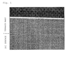
Fig. 1 is an example of the shape of a terrace part of an SOI wafer manufactured by a method for manufacturing SOI wafer of an example 1; and -
Fig. 2 is an example of the shape of a terrace part of an SOI wafer manufactured by a method for manufacturing SOI wafer of a comparative example 2. - In the following, although a method for manufacturing SOI wafer and an SOI wafer of the present invention will be described in detail, the present invention is not limited thereto.
- The present inventors, as a result of performance of keen examination, discovered that the SOI wafer that is small in SOI layer film thickness range, is small in surface roughness of the SOI layer surface, is smooth in shape of the terrace part, and has no defects such as the voids, the blisters and so forth in the SOI layer can be manufactured, by a method for manufacturing SOI wafer, comprising steps of forming an ion implanted layer by implanting hydrogen ions from a surface of a bond wafer consisting of a silicon single crystal substrate, bonding an ion implanted surface of the bond wafer and a surface of a base wafer consisting of a silicon single crystal wafer through an oxide film, and thereafter delaminating the bond wafer at the ion implanted layer by performing delamination heat treatment, wherein, after plasma treatment has been performed on at least one surface of a bonding interface of the bond wafer and a bonding interface of the base wafer, bonding is performed through the oxide film, and the bond wafer is delaminated at the ion implanted layer by the delamination heat treatment comprising a first heat treatment at 250°C or less for 2 hours or more and a second heat treatment at 400°C to 450°C for 30 minutes or more. And the present inventors have accomplished the present invention.
- As described above, the present invention performs ion implantation of only hydrogen ions into the bond wafer, performs plasma treatment on at least one of the bonding surfaces of the bond wafer and the base wafer, and thereafter bonds them through the oxide film, and performs delamination heat treatment.
- By performing ion implantation of only hydrogen ions on the bond wafer (without implanting helium ions) in this way, influence of generation of the voids and the blisters caused by implantation of helium ions is not exerted, and the defects such as the voids and the blisters are not generated in the SOI layer.
- In addition, as described above, the present invention enhances the bonding strength of the wafers by performing plasma treatment on at least one of the bonding interfaces of the bond wafer and the base wafer, and thereafter performing delamination treatment in comparatively low-temperature heat treatment. Thereby, the present invention can make the surface roughness of the SOI layer surface small.
- Here, in the delamination heat treatment of the present invention, at least 2-hour annealing is performed at not more than 250°C as the first step, and next, at least 30-minute annealing is performed in a temperature range of 400 to 450°C as the second step, thereby the ion implanted layer is made brittle and delamination is performed.
- The wafer bonded after performing plasma treatment is more improved in bonding strength than a normally bonded wafer. The first embrittlement of ion implanted layer and enhancing of the bonding strength of the wafer occur by treating the wafer at not more than 250°C as the first step, thereafter, the bonding strength is more improved by 400 to 450°C heat treatment, embrittlement of the ion implanted layer is completed and wafer delamination occurs.
- In the present invention, in this way, plasma treatment is performed on the wafer so as to enhance the bonding strength of the wafers, and heat treatment that raises the temperature at comparatively low-temperature in 2 steps (the aforementioned first step, second step) is performed so as to make the ion implanted layer brittle stepwise and delamination is performed, and thereby the surface roughness of the SOI layer surface can be made small.
- In addition, since the present invention delaminates the ion implanted layer by heat treatment (not mechanically, forcedly delaminating it by inserting the wedge) in delamination, the SOI layer film thickness can be made small and the shape of the terrace part can be made smooth.
- Incidentally, taking efficiency of delamination heat treatment into account, it is preferable that the heat treatment time in the first step and second step of delamination heat treatment be not more than 8 hours in either step, and it is more preferable that it be not more than 4 hours. Therefore, it is preferable the heat treatment temperature in the first step be at least 150°C.
- The aforementioned plasma treatment is preferable to perform nitrogen plasma treatment on the wafer having the oxide film, and to perform oxygen plasma treatment on the wafer (including a wafer that only a native oxide film has been grown) with no oxide film.
- By performing such plasma treatment and thereafter performing bonding of the wafers, the particularly high bonding strength can be obtained. The wafer that has been treated under such condition makes it possible to complete wafer delamination at a comparatively low temperature and in a short time, and to manufacture the SOI wafer that is further smaller in roughness of the delamination surface.
- The SOI wafer just after delamination that has been manufactured in this way is small in surface roughness of the SOI layer surface, and is favorable in film thickness distribution of the SOI layer, terrace shape, and is free from generation of the blisters and the voids. In addition, since the surface roughness of the SOI layer surface is small, the SOI wafer as the finished product can make the surface roughness of the SOI layer surface sufficiently small even when performing flattening treatment only by heat treatment not using CMP.
- The SOI wafer that has been manufactured in this way can be made as the one that the surface roughness (RMS) of the SOI layer surface that is the delamination surface before performing flattening treatment is not more than 3 nm, and the film thickness range of the SOI layer is not more than 1.5 nm.
- The SOI wafer of high quality can be manufactured by performing flattening treatment on the delamination surface of the SOI wafer after the aforementioned delamination without performing CMP.
- As flattening treatment, for example, treatment of performing sacrificial oxidation treatment + Ar annealing + sacrificial oxidation treatment can be given. The SOI wafer that has been produced in this way is convenient because the film thickness uniformity of the SOI layer is excellent, and the SOI layer film thickness range is made further smaller.
- In such an SOI wafer, since the SOI layer film thickness range and the surface roughness of the SOI layer surface are extremely small, further the shape of the terrace part is smooth, and there are no defects such as the voids, the blisters and so forth in the SOI layer. Therefore, it is made high in quality as the finished product to be shipped to the device manufacturers.
- Although, in the following, the present invention will be more specifically described by showing examples, comparative examples and experimental examples, the present invention is not limited thereto.
- An SOI wafer was produced by using a Si single crystal wafer of 300 mm in diameter and <100> in crystal orientation. In that occasion, a thermal oxide film of 150 nm was grown on a bond wafer in a heat treat furnace, and hydrogen ions (H+ ions) were ion-implanted into this wafer in dose amount of 5 × 10¹⁶/cm2 and with acceleration energy of 40 keV. A base wafer consisting of a Si single crystal wafer was prepared, oxygen plasma treatment was performed only on the base wafer, and thereafter, bonding with the ion-implanted bond wafer was performed. After an annealing at 200°C for 4 hours as the first step had been performed on this bonded wafer, the temperature was raised at a rate of temperature rise of 10°C/min, and an annealing at 400°C for 6 hours as the second step was performed. The wafer was delaminated by this heat treatment and became an initial SOI wafer.
- An SOI wafer was produced by using a Si single crystal wafer of 300 mm in diameter and <100> in crystal orientation. In that occasion, a thermal oxide film of 150 nm was grown on a bond wafer in the heat treat furnace, and hydrogen ions (H+ ions) were ion-implanted into this wafer in dose amount of 5 × 10¹⁶/cm2 and with acceleration energy of 40 keV. A base wafer consisting of a Si single crystal wafer was prepared and bonding with the ion-implanted bond wafer was performed (no plasma treatment). After an annealing at 350°C for 2 hours as the first step had been performed on this bonded wafer, the temperature was raised at a rate of temperature rise of 10°C/min, and an annealing at 500°C for 30 minutes as the second step was performed. The wafer was delaminated by this heat treatment and became an initial SOI wafer.
- An SOI wafer was produced by using a Si single crystal wafer of 300 mm in diameter and <100> in crystal orientation. In that occasion, a thermal oxide film of 150 nm was grown on a bond wafer in the heat treat furnace, and hydrogen ions (H+ ions) were ion-implanted into this wafer in dose amount of 7.5 × 10¹⁶/cm2 and with acceleration energy of 40 keV. A base wafer consisting of a Si single crystal wafer was prepared, oxygen plasma treatment was performed only on the base wafer, and thereafter, bonding with the ion-implanted bond wafer was performed. An annealing at 350°C for 2 hours was only performed on this bonded wafer. Wafer separation was not yet done in this state, and thereafter wafer delamination was performed using a wedge at a room temperature.
- An SOI wafer was produced by using a Si single crystal wafer of 300 mm in diameter and <100> in crystal orientation. In that occasion, a thermal oxide film of 150 nm was grown on a bond wafer in the heat treat furnace, and helium ions (He+ ions) and hydrogen ions (H+ ions) were ion-implanted into this wafer in dose amount of 0.9 × 10¹⁶/cm2 and in dose amount of 0.9 × 10¹⁶/cm2, and with acceleration energy of 40 keV. A base wafer consisting of a Si single crystal wafer was prepared, and bonding with the ion-implanted bond wafer was performed (no plasma treatment). After an annealing at 350°C for 2 hours as the first step had been performed on this bonded wafer, the temperature was raised at a rate of temperature rise of 10°C/min, and annealing at 500°C for 30 minutes as the second step was performed. The wafer was delaminated by this heat treatment and became an initial SOI wafer.
- A result of evaluation of four items of the AFM roughness, the SOI layer film thickness range, the shape of the terrace part, the defects (voids, blisters) of the example 1, comparative example 1-3 was tabulated in the following Table 1.
- Incidentally, the AFM roughness in Table 1 is a value that the surface roughness of a 30 µm-square region measured through an AFM (an atomic force microscope) has been expressed in RMS (Root Mean Square).
[Table 1] AFM Roughness 30x30 µm RMS (nm) SOI Film Thickness Range (nm) Shape of Terrace Part Defects (Voids, Blisters) Example 1 2.5 1.3 Favorable None Comparative Example 1 5.3 1.1 Favorable None Comparative Example 2 2.5 2.1 Noticeable ruggedness None Comparative Example 3 3.1 1.2 Favorable Generated by 2-3% - In regard to the AFM roughness, Comparative Example 1 results in about two times as large as the other examples, the surface roughness is large and it can be anticipated that a load will be exerted onto a subsequent flattening process.
- In regard to the film thickness distribution, only Comparative Example 2 had become large. The cause therefor lies in that when performing wafer separation, wafer separation occurs around the wedge at the moment that the wedge has been inserted, and thereafter wafer separation is performed by further advancing the wedge in a central direction of the wafer. The film thickness is sharply changed at a boundary between this initially wafer separated region and a subsequently separated region. This is a cause for large film thickness distribution.
- In regard to the shape of the terrace part, noticeable ruggedness was generated only in Comparative Example 2 (
Fig. 2 ). It is thought that this is because mechanical compelling force is exerted by forcedly performing wafer separation by using the wedge at the room temperature. In comparison with it, the shapes of the terrace parts in other examples are favorable (Fig. 1 ). It is thought that the rugged shape is not generated because delamination occurs smoothly by heat treatment. - In regard to generation of the defects, they were generated only in Comparative Example 3. It is thought that ion implantation of He (helium) and H (hydrogen) is performed and it leads to performance of treatment two times in a process that particle adhesion is the most liable to occur in the manufacturing process, and therefore particle-induced generation of voids and blisters is more increased than other examples. Incidentally, though not shown in the table, although generation of the blisters was reduced in other examples that had been performed under the same conditions as Comparative Example 3 excepting that the plasma treatment was performed before bonding, generation of the voids was increased and there was no change in total number of defects of the voids and the blisters.
- An experiment that the first step and the second step for wafer separation (delamination) are combined was performed under the following conditions.
- An SOI wafer was produced by using Si single crystal wafers of 300 mm in diameter and <100> in crystal orientation as a bond wafer and a base wafer.
- First, a thermal oxide film of 150 nm was grown on the bond wafer in the heat treat furnace. Hydrogen was ion-implanted into this wafer in dose amount of 5 × 10¹⁶/cm2 and with acceleration energy of 40 keV. The base wafer (with no oxide film) was prepared, nitrogen plasma treatment was performed on the base wafer, and thereafter bonding was performed. As delamination heat treatment, 2-hour annealing was performed on this bonded wafer within a range of 150 to 350°C as the first step, the temperature was raised at 10°C /min, and 350 to 500°C annealing was performed as the second step (see Table 2 for heat treatment conditions of the first step, the second step). By this heat treatment, it was delaminated at the ion implanted layer and an initial SOI wafer was produced (there are the ones that cannot be delaminated depending on the heat treatment condition). A sacrificial oxidation treatment at 900°C for 2 hours(thermal oxidation + oxide film removal), an annealing at 1200°C for 1 hour under an Ar atmosphere, and 950°C sacrificial oxidation treatment for film thickness adjustment were sequentially performed on this initial SOI wafer so as to produce finished products of the SOI wafer of 88 nm in SOI layer film thickness, and the surface roughness (RMS) of the SOI layer surfaces thereof was measured and compared through the AFM within a range of 30 µm × 30 µm. A result is shown in the following Table 2.

- The surface roughness (RMS) of the SOI layer surface when heat treatment was performed for 2 hours within a range of 150°C to 250°C as the first step, and heat treatment was performed for at least 30 minutes and not more than 4 hours at 400°C to 450°C as the second step is extremely small.
- Finished products of the SOI wafer were produced under the same conditions as in Experimental Example 1 excepting that the heat treatment time in the first step was set to 4 hours, and the second step was set to 3 conditions of 350°C and 4 hours, 400°C and 0.5 hours, 450°C and 0.5 hours were set, and the surface roughness (RMS) of the SOI layer surfaces thereof was measured and compared through the AFM within the range of 30 µm × 30 µm. A result is shown in the following Table 3.

- The surface roughness (RMS) of the SOI layer surface when heat treatment was performed for 4 hours within a range of 150°C to 250°C as the first step, and heat treatment was performed for 30 minutes at 400°C to 450°C as the second step is extremely small. Incidentally, when the heat treatment temperature in the second step after heat treatment in the first step is 350°C (less than 400°C), delamination itself did not occur even when heat treatment was performed for 4 hours.
- Finished products of the SOI wafer were produced under the same conditions as in Experimental Example 1 excepting that the heat treatment time in the first step was set to 1 hour, and the second step was set to 2 conditions of 350°C and 4 hours, 400°C and 0.5 hours, and the surface roughnesses (RMS) of the SOI layer surfaces thereof were measured and compared through the AFM within the range of 30 µm × 30 µm. A result is shown in the following Table 4.

- The result was such that when the heat treatment time in the first step is 1 hour (less than 2 hours), the wafer is not delaminated partially even when heat treatment is performed for 30 minutes at 400°C in the second step. In addition, when the heat treatment time in the first step is 1 hour (less than 2 hour) and the heat treatment temperature in the second step is 350°C (less than 400°C), delamination itself did not occur even when heat treatment was performed for 4 hours.
- Finished products of the SOI wafer were produced under the same conditions (some conditions were not performed) as in Experimental Example 1 excepting that plasma treatment is not performed before bonding , and the surface roughness (RMS) of the SOI layer surfaces thereof was measured and compared through the AFM within the range of 30 µm × 30 µm. A result is shown in the following Table 5.

- Even when heat treatment was performed for 2 hours within a range of 150°C to 250°C as the first step and heat treatment was performed for 4 hours at 400°C, or 1 hour at 450°C as the second step, the wafer was not delaminated or the surface roughness (RMS) of the SOI layer surface was large although it had been delaminated, unless plasma treatment was performed before bonding.
- In order to confirm the effects of the plasma treatment conditions, finished products of the SOI were produced under the following conditions.
- SOI was produced by using Si single crystal wafers of 300 mm in diameter and <100> in crystal orientation as the bond wafer and the base wafer.
- First, a thermal oxide film of 150 nm was grown on the bond wafer in the heat treat furnace. Hydrogen was ion-implanted into this bond wafer in dose amount of 5 × 10¹⁶/cm2 and with acceleration energy of 40 keV. The base wafer (with no oxide film) was prepared, plasma treatment was performed on both of them, and thereafter they were bonded each other.
- Plasma conditions were as in the following Table 6.
[Table 6] Bond Wafer (with oxide film) Base Wafer (without oxide film) Condition (1) Nitrogen Plasma Nitrogen Plasma Condition (2) Nitrogen Plasma Oxygen Plasma Condition (3) Oxygen Plasma Nitrogen Plasma Condition (4) Oxygen Plasma Oxygen Plasma - As delamination heat treatment, after an annealing at 200°C for 4 hours had been performed on this bonded wafer as the first step, the temperature was then raised at the rate of temperature rise of 10°C /min, and thereafter an annealing at 400°C for 4 hours was performed as the second step. By this heat treatment, it was delaminated at the ion implanted layer, and an initial SOI wafer was produced. Thereafter an sacrificial oxidation treatment at 900°C for 2 hours, an annealing at 1200°C for 1 hour under the Ar atmosphere, and 950°C sacrificial oxidation treatment for film thickness adjustment were sequentially performed on this initial SOI wafer so as to produce finished products of the SOI wafer of 88 nm in SOI layer film thickness, and the surface roughness (RMS) of the SOI layer surfaces thereof was measured and compared through the AFM within the range of 30 µm × 30 µm.
- The surface roughness (RMS) were made as follows.
Condition (1) 0.17 nm Condition (2) 0.14 nm Condition (3) 0.17 nm Condition (4) 0.15 nm - From the above, it was found that the surface roughness (RMS) becomes the smallest by treating the oxide film with nitrogen plasmas and the wafer with no oxide film with oxygen plasmas.
- Incidentally, the present invention, the above mentioned embodiment is illustrative and ones having configurations that are substantially the same as the technical ideas described in the scope of patent claims of the present invention and exhibiting the same operational effects are included in the technical scope of the present invention whatever they may be.
Claims (4)
- A method for manufacturing SOI wafer, comprising steps of forming an ion implanted layer by implanting hydrogen ions from a surface of a bond wafer consisting of a silicon single crystal substrate, bonding an ion implanted surface of the bond wafer and a surface of a base wafer consisting of a silicon single crystal wafer through an oxide film, and thereafter delaminating the bond wafer at the ion implanted layer by performing delamination heat treatment, wherein,
after plasma treatment has been performed on at least one surface of a bonding interface of the bond wafer and a bonding interface of the base wafer, bonding is performed through the oxide film, and
the bond wafer is delaminated at the ion implanted layer by the delamination heat treatment comprising a first heat treatment at 250°C or less for 2 hours or more and a second heat treatment at 400°C to 450°C for 30 minutes or more. - The method for manufacturing SOI wafer according to claim 1, wherein, as the plasma treatment, nitrogen plasma treatment is performed on a wafer having the oxide film, and oxygen plasma treatment is performed on a wafer having no oxide film.
- The method for manufacturing SOI wafer according to claim 1 or 2, wherein flattening treatment without CMP is performed on a delamination surface of the SOI wafer after the delamination.
- An SOI wafer manufactured by the method for manufacturing SOI wafer according to claim 1 or 2, wherein a surface roughness (RMS) of an SOI layer surface that is a delamination surface is not more than 3 nm, and a film thickness range of the SOI layer is not more than 1.5 nm.
Applications Claiming Priority (2)
| Application Number | Priority Date | Filing Date | Title |
|---|---|---|---|
| JP2013018833A JP6056516B2 (en) | 2013-02-01 | 2013-02-01 | Manufacturing method of SOI wafer and SOI wafer |
| PCT/JP2013/007248 WO2014118851A1 (en) | 2013-02-01 | 2013-12-10 | Production method of soi wafer, and soi wafer |
Publications (3)
| Publication Number | Publication Date |
|---|---|
| EP2953153A1 true EP2953153A1 (en) | 2015-12-09 |
| EP2953153A4 EP2953153A4 (en) | 2016-10-19 |
| EP2953153B1 EP2953153B1 (en) | 2021-05-26 |
Family
ID=51261601
Family Applications (1)
| Application Number | Title | Priority Date | Filing Date |
|---|---|---|---|
| EP13874124.4A Active EP2953153B1 (en) | 2013-02-01 | 2013-12-10 | Production method of soi wafer, and soi wafer |
Country Status (6)
| Country | Link |
|---|---|
| US (1) | US20150340279A1 (en) |
| EP (1) | EP2953153B1 (en) |
| JP (1) | JP6056516B2 (en) |
| KR (1) | KR102019653B1 (en) |
| CN (1) | CN104956464B (en) |
| WO (1) | WO2014118851A1 (en) |
Families Citing this family (7)
| Publication number | Priority date | Publication date | Assignee | Title |
|---|---|---|---|---|
| JP3471869B2 (en) | 1993-11-05 | 2003-12-02 | 蛇の目ミシン工業株式会社 | Operation detection start sewing machine |
| JP6473970B2 (en) * | 2015-10-28 | 2019-02-27 | 信越半導体株式会社 | Manufacturing method of bonded SOI wafer |
| CN106960811A (en) * | 2016-01-12 | 2017-07-18 | 沈阳硅基科技有限公司 | A kind of preparation method of SOI silicon chip |
| CN107154379B (en) * | 2016-03-03 | 2020-01-24 | 上海新昇半导体科技有限公司 | Silicon substrate with top layer on insulating layer and manufacturing method thereof |
| EP3571900B1 (en) | 2017-01-18 | 2024-11-13 | SHINE Technologies, LLC | Device comprising a waveguide with an inverted impedance matcher and system with the same |
| KR101952492B1 (en) * | 2017-01-20 | 2019-02-26 | 한양대학교 산학협력단 | Wafer bonding method, and three-dimensional semiconductor device manufactured by the same |
| CN114664657A (en) * | 2021-10-29 | 2022-06-24 | 中国科学院上海微系统与信息技术研究所 | A kind of wafer surface treatment method |
Family Cites Families (19)
| Publication number | Priority date | Publication date | Assignee | Title |
|---|---|---|---|---|
| FR2681472B1 (en) | 1991-09-18 | 1993-10-29 | Commissariat Energie Atomique | PROCESS FOR PRODUCING THIN FILMS OF SEMICONDUCTOR MATERIAL. |
| FR2755537B1 (en) * | 1996-11-05 | 1999-03-05 | Commissariat Energie Atomique | METHOD FOR MANUFACTURING A THIN FILM ON A SUPPORT AND STRUCTURE THUS OBTAINED |
| JP3900741B2 (en) | 1999-05-21 | 2007-04-04 | 信越半導体株式会社 | Manufacturing method of SOI wafer |
| JP4304879B2 (en) | 2001-04-06 | 2009-07-29 | 信越半導体株式会社 | Method for determining the implantation amount of hydrogen ions or rare gas ions |
| EP1408551B1 (en) * | 2001-07-17 | 2014-07-02 | Shin-Etsu Handotai Co., Ltd. | Method for producing bonding wafer |
| FR2839385B1 (en) * | 2002-05-02 | 2004-07-23 | Soitec Silicon On Insulator | PROCESS FOR TAKING OFF MATERIAL LAYERS |
| FR2874455B1 (en) | 2004-08-19 | 2008-02-08 | Soitec Silicon On Insulator | HEAT TREATMENT BEFORE BONDING TWO PLATES |
| EP1652230A2 (en) | 2003-07-29 | 2006-05-03 | S.O.I.Tec Silicon on Insulator Technologies | Method for obtaining a thin high-quality layer by co-implantation and thermal annealing |
| CN101027768B (en) | 2004-09-21 | 2010-11-03 | S.O.I.Tec绝缘体上硅技术公司 | Thin layer transfer method with co-injection step under conditions to avoid bubble formation and limit roughness |
| JP2006210898A (en) | 2004-12-28 | 2006-08-10 | Shin Etsu Chem Co Ltd | Manufacturing method of SOI wafer and SOI wafer |
| US7767542B2 (en) | 2007-04-20 | 2010-08-03 | Semiconductor Energy Laboratory Co., Ltd | Manufacturing method of SOI substrate |
| US8163628B2 (en) * | 2007-11-01 | 2012-04-24 | Semiconductor Energy Laboratory Co., Ltd. | Method for manufacturing semiconductor substrate |
| JP5654206B2 (en) * | 2008-03-26 | 2015-01-14 | 株式会社半導体エネルギー研究所 | Method for manufacturing SOI substrate and semiconductor device using the SOI substrate |
| JP5496598B2 (en) * | 2008-10-31 | 2014-05-21 | 信越化学工業株式会社 | Manufacturing method of silicon thin film transfer insulating wafer |
| JP5493343B2 (en) * | 2008-12-04 | 2014-05-14 | 信越半導体株式会社 | Manufacturing method of bonded wafer |
| JP5244650B2 (en) | 2009-02-26 | 2013-07-24 | 信越半導体株式会社 | Manufacturing method of SOI wafer |
| JP5532680B2 (en) * | 2009-05-27 | 2014-06-25 | 信越半導体株式会社 | Manufacturing method of SOI wafer and SOI wafer |
| JP5706670B2 (en) * | 2009-11-24 | 2015-04-22 | 株式会社半導体エネルギー研究所 | Method for manufacturing SOI substrate |
| JP5703853B2 (en) * | 2011-03-04 | 2015-04-22 | 信越半導体株式会社 | Manufacturing method of bonded wafer |
-
2013
- 2013-02-01 JP JP2013018833A patent/JP6056516B2/en active Active
- 2013-12-10 WO PCT/JP2013/007248 patent/WO2014118851A1/en not_active Ceased
- 2013-12-10 CN CN201380071248.0A patent/CN104956464B/en active Active
- 2013-12-10 KR KR1020157020474A patent/KR102019653B1/en active Active
- 2013-12-10 EP EP13874124.4A patent/EP2953153B1/en active Active
- 2013-12-10 US US14/655,880 patent/US20150340279A1/en not_active Abandoned
Also Published As
| Publication number | Publication date |
|---|---|
| KR102019653B1 (en) | 2019-09-09 |
| CN104956464A (en) | 2015-09-30 |
| WO2014118851A1 (en) | 2014-08-07 |
| EP2953153A4 (en) | 2016-10-19 |
| JP2014150193A (en) | 2014-08-21 |
| JP6056516B2 (en) | 2017-01-11 |
| US20150340279A1 (en) | 2015-11-26 |
| EP2953153B1 (en) | 2021-05-26 |
| KR20150112968A (en) | 2015-10-07 |
| CN104956464B (en) | 2017-09-22 |
Similar Documents
| Publication | Publication Date | Title |
|---|---|---|
| EP2953153B1 (en) | Production method of soi wafer, and soi wafer | |
| CN100419960C (en) | Method for manufacturing SOI wafer | |
| US10236205B2 (en) | Thin film and method for manufacturing thin film | |
| JP2006156770A (en) | Direct bonding wafer manufacturing method and direct bonding wafer | |
| JP2006005127A (en) | Manufacturing method of bonded wafer | |
| EP3118889B1 (en) | Process for producing bonded soi wafer | |
| EP2887383A1 (en) | Soi wafer manufacturing method | |
| EP2251895B1 (en) | Method for manufacturing bonded wafer | |
| JP5261960B2 (en) | Manufacturing method of semiconductor substrate | |
| EP3309820A1 (en) | Method of manufacturing soi wafer | |
| EP2579296A1 (en) | Method for manufacturing bonded wafer | |
| US8697544B2 (en) | Method for manufacturing bonded wafer | |
| JP5263509B2 (en) | Manufacturing method of bonded wafer | |
| TW201445636A (en) | Fitting wafer manufacturing method | |
| JP2007073768A (en) | Method for manufacturing laminated soi wafer | |
| JP2016082093A (en) | Manufacturing method of bonded wafer | |
| JP6927143B2 (en) | Manufacturing method of bonded SOI wafer | |
| JP2013055184A (en) | Manufacturing method of laminated wafer | |
| WO2017217129A1 (en) | Bonded wafer manufacturing method | |
| JP5531642B2 (en) | Manufacturing method of bonded wafer | |
| EP3370249B1 (en) | Bonded soi wafer manufacturing method | |
| JP5572914B2 (en) | Manufacturing method of directly bonded wafer | |
| JP2006013179A (en) | Method for manufacturing soi wafer | |
| KR20160052551A (en) | Bonded wafer manufacturing method | |
| JP2014212172A (en) | Method of manufacturing laminated wafer |
Legal Events
| Date | Code | Title | Description |
|---|---|---|---|
| PUAI | Public reference made under article 153(3) epc to a published international application that has entered the european phase |
Free format text: ORIGINAL CODE: 0009012 |
|
| 17P | Request for examination filed |
Effective date: 20150722 |
|
| AK | Designated contracting states |
Kind code of ref document: A1 Designated state(s): AL AT BE BG CH CY CZ DE DK EE ES FI FR GB GR HR HU IE IS IT LI LT LU LV MC MK MT NL NO PL PT RO RS SE SI SK SM TR |
|
| AX | Request for extension of the european patent |
Extension state: BA ME |
|
| DAX | Request for extension of the european patent (deleted) | ||
| A4 | Supplementary search report drawn up and despatched |
Effective date: 20160916 |
|
| RIC1 | Information provided on ipc code assigned before grant |
Ipc: H01L 21/02 20060101AFI20160912BHEP Ipc: H01L 27/12 20060101ALI20160912BHEP Ipc: H01L 21/265 20060101ALI20160912BHEP Ipc: H01L 29/34 20060101ALI20160912BHEP Ipc: H01L 21/762 20060101ALI20160912BHEP |
|
| STAA | Information on the status of an ep patent application or granted ep patent |
Free format text: STATUS: EXAMINATION IS IN PROGRESS |
|
| 17Q | First examination report despatched |
Effective date: 20190527 |
|
| GRAP | Despatch of communication of intention to grant a patent |
Free format text: ORIGINAL CODE: EPIDOSNIGR1 |
|
| STAA | Information on the status of an ep patent application or granted ep patent |
Free format text: STATUS: GRANT OF PATENT IS INTENDED |
|
| INTG | Intention to grant announced |
Effective date: 20201211 |
|
| GRAS | Grant fee paid |
Free format text: ORIGINAL CODE: EPIDOSNIGR3 |
|
| GRAA | (expected) grant |
Free format text: ORIGINAL CODE: 0009210 |
|
| STAA | Information on the status of an ep patent application or granted ep patent |
Free format text: STATUS: THE PATENT HAS BEEN GRANTED |
|
| AK | Designated contracting states |
Kind code of ref document: B1 Designated state(s): AL AT BE BG CH CY CZ DE DK EE ES FI FR GB GR HR HU IE IS IT LI LT LU LV MC MK MT NL NO PL PT RO RS SE SI SK SM TR |
|
| REG | Reference to a national code |
Ref country code: GB Ref legal event code: FG4D |
|
| RIN1 | Information on inventor provided before grant (corrected) |
Inventor name: KOBAYASHI, NORIHIRO Inventor name: YOKOKAWA, ISAO Inventor name: AGA, HIROJI |
|
| REG | Reference to a national code |
Ref country code: CH Ref legal event code: EP |
|
| REG | Reference to a national code |
Ref country code: DE Ref legal event code: R096 Ref document number: 602013077704 Country of ref document: DE |
|
| REG | Reference to a national code |
Ref country code: AT Ref legal event code: REF Ref document number: 1397066 Country of ref document: AT Kind code of ref document: T Effective date: 20210615 |
|
| REG | Reference to a national code |
Ref country code: IE Ref legal event code: FG4D |
|
| REG | Reference to a national code |
Ref country code: DE Ref legal event code: R082 Ref document number: 602013077704 Country of ref document: DE Representative=s name: WUESTHOFF & WUESTHOFF, PATENTANWAELTE PARTG MB, DE |
|
| REG | Reference to a national code |
Ref country code: LT Ref legal event code: MG9D |
|
| REG | Reference to a national code |
Ref country code: AT Ref legal event code: MK05 Ref document number: 1397066 Country of ref document: AT Kind code of ref document: T Effective date: 20210526 |
|
| PG25 | Lapsed in a contracting state [announced via postgrant information from national office to epo] |
Ref country code: HR Free format text: LAPSE BECAUSE OF FAILURE TO SUBMIT A TRANSLATION OF THE DESCRIPTION OR TO PAY THE FEE WITHIN THE PRESCRIBED TIME-LIMIT Effective date: 20210526 Ref country code: BG Free format text: LAPSE BECAUSE OF FAILURE TO SUBMIT A TRANSLATION OF THE DESCRIPTION OR TO PAY THE FEE WITHIN THE PRESCRIBED TIME-LIMIT Effective date: 20210826 Ref country code: AT Free format text: LAPSE BECAUSE OF FAILURE TO SUBMIT A TRANSLATION OF THE DESCRIPTION OR TO PAY THE FEE WITHIN THE PRESCRIBED TIME-LIMIT Effective date: 20210526 Ref country code: LT Free format text: LAPSE BECAUSE OF FAILURE TO SUBMIT A TRANSLATION OF THE DESCRIPTION OR TO PAY THE FEE WITHIN THE PRESCRIBED TIME-LIMIT Effective date: 20210526 Ref country code: FI Free format text: LAPSE BECAUSE OF FAILURE TO SUBMIT A TRANSLATION OF THE DESCRIPTION OR TO PAY THE FEE WITHIN THE PRESCRIBED TIME-LIMIT Effective date: 20210526 |
|
| REG | Reference to a national code |
Ref country code: NL Ref legal event code: MP Effective date: 20210526 |
|
| PG25 | Lapsed in a contracting state [announced via postgrant information from national office to epo] |
Ref country code: SE Free format text: LAPSE BECAUSE OF FAILURE TO SUBMIT A TRANSLATION OF THE DESCRIPTION OR TO PAY THE FEE WITHIN THE PRESCRIBED TIME-LIMIT Effective date: 20210526 Ref country code: RS Free format text: LAPSE BECAUSE OF FAILURE TO SUBMIT A TRANSLATION OF THE DESCRIPTION OR TO PAY THE FEE WITHIN THE PRESCRIBED TIME-LIMIT Effective date: 20210526 Ref country code: PT Free format text: LAPSE BECAUSE OF FAILURE TO SUBMIT A TRANSLATION OF THE DESCRIPTION OR TO PAY THE FEE WITHIN THE PRESCRIBED TIME-LIMIT Effective date: 20210927 Ref country code: NO Free format text: LAPSE BECAUSE OF FAILURE TO SUBMIT A TRANSLATION OF THE DESCRIPTION OR TO PAY THE FEE WITHIN THE PRESCRIBED TIME-LIMIT Effective date: 20210826 Ref country code: PL Free format text: LAPSE BECAUSE OF FAILURE TO SUBMIT A TRANSLATION OF THE DESCRIPTION OR TO PAY THE FEE WITHIN THE PRESCRIBED TIME-LIMIT Effective date: 20210526 Ref country code: LV Free format text: LAPSE BECAUSE OF FAILURE TO SUBMIT A TRANSLATION OF THE DESCRIPTION OR TO PAY THE FEE WITHIN THE PRESCRIBED TIME-LIMIT Effective date: 20210526 Ref country code: GR Free format text: LAPSE BECAUSE OF FAILURE TO SUBMIT A TRANSLATION OF THE DESCRIPTION OR TO PAY THE FEE WITHIN THE PRESCRIBED TIME-LIMIT Effective date: 20210827 Ref country code: IS Free format text: LAPSE BECAUSE OF FAILURE TO SUBMIT A TRANSLATION OF THE DESCRIPTION OR TO PAY THE FEE WITHIN THE PRESCRIBED TIME-LIMIT Effective date: 20210926 |
|
| PG25 | Lapsed in a contracting state [announced via postgrant information from national office to epo] |
Ref country code: NL Free format text: LAPSE BECAUSE OF FAILURE TO SUBMIT A TRANSLATION OF THE DESCRIPTION OR TO PAY THE FEE WITHIN THE PRESCRIBED TIME-LIMIT Effective date: 20210526 |
|
| PG25 | Lapsed in a contracting state [announced via postgrant information from national office to epo] |
Ref country code: SM Free format text: LAPSE BECAUSE OF FAILURE TO SUBMIT A TRANSLATION OF THE DESCRIPTION OR TO PAY THE FEE WITHIN THE PRESCRIBED TIME-LIMIT Effective date: 20210526 Ref country code: SK Free format text: LAPSE BECAUSE OF FAILURE TO SUBMIT A TRANSLATION OF THE DESCRIPTION OR TO PAY THE FEE WITHIN THE PRESCRIBED TIME-LIMIT Effective date: 20210526 Ref country code: CZ Free format text: LAPSE BECAUSE OF FAILURE TO SUBMIT A TRANSLATION OF THE DESCRIPTION OR TO PAY THE FEE WITHIN THE PRESCRIBED TIME-LIMIT Effective date: 20210526 Ref country code: EE Free format text: LAPSE BECAUSE OF FAILURE TO SUBMIT A TRANSLATION OF THE DESCRIPTION OR TO PAY THE FEE WITHIN THE PRESCRIBED TIME-LIMIT Effective date: 20210526 Ref country code: DK Free format text: LAPSE BECAUSE OF FAILURE TO SUBMIT A TRANSLATION OF THE DESCRIPTION OR TO PAY THE FEE WITHIN THE PRESCRIBED TIME-LIMIT Effective date: 20210526 Ref country code: ES Free format text: LAPSE BECAUSE OF FAILURE TO SUBMIT A TRANSLATION OF THE DESCRIPTION OR TO PAY THE FEE WITHIN THE PRESCRIBED TIME-LIMIT Effective date: 20210526 Ref country code: RO Free format text: LAPSE BECAUSE OF FAILURE TO SUBMIT A TRANSLATION OF THE DESCRIPTION OR TO PAY THE FEE WITHIN THE PRESCRIBED TIME-LIMIT Effective date: 20210526 |
|
| REG | Reference to a national code |
Ref country code: DE Ref legal event code: R097 Ref document number: 602013077704 Country of ref document: DE |
|
| PLBE | No opposition filed within time limit |
Free format text: ORIGINAL CODE: 0009261 |
|
| STAA | Information on the status of an ep patent application or granted ep patent |
Free format text: STATUS: NO OPPOSITION FILED WITHIN TIME LIMIT |
|
| 26N | No opposition filed |
Effective date: 20220301 |
|
| PG25 | Lapsed in a contracting state [announced via postgrant information from national office to epo] |
Ref country code: IS Free format text: LAPSE BECAUSE OF FAILURE TO SUBMIT A TRANSLATION OF THE DESCRIPTION OR TO PAY THE FEE WITHIN THE PRESCRIBED TIME-LIMIT Effective date: 20210926 Ref country code: AL Free format text: LAPSE BECAUSE OF FAILURE TO SUBMIT A TRANSLATION OF THE DESCRIPTION OR TO PAY THE FEE WITHIN THE PRESCRIBED TIME-LIMIT Effective date: 20210526 |
|
| PG25 | Lapsed in a contracting state [announced via postgrant information from national office to epo] |
Ref country code: MC Free format text: LAPSE BECAUSE OF FAILURE TO SUBMIT A TRANSLATION OF THE DESCRIPTION OR TO PAY THE FEE WITHIN THE PRESCRIBED TIME-LIMIT Effective date: 20210526 Ref country code: IT Free format text: LAPSE BECAUSE OF FAILURE TO SUBMIT A TRANSLATION OF THE DESCRIPTION OR TO PAY THE FEE WITHIN THE PRESCRIBED TIME-LIMIT Effective date: 20210526 |
|
| REG | Reference to a national code |
Ref country code: CH Ref legal event code: PL |
|
| GBPC | Gb: european patent ceased through non-payment of renewal fee |
Effective date: 20211210 |
|
| REG | Reference to a national code |
Ref country code: BE Ref legal event code: MM Effective date: 20211231 |
|
| PG25 | Lapsed in a contracting state [announced via postgrant information from national office to epo] |
Ref country code: LU Free format text: LAPSE BECAUSE OF NON-PAYMENT OF DUE FEES Effective date: 20211210 Ref country code: IE Free format text: LAPSE BECAUSE OF NON-PAYMENT OF DUE FEES Effective date: 20211210 Ref country code: GB Free format text: LAPSE BECAUSE OF NON-PAYMENT OF DUE FEES Effective date: 20211210 |
|
| PG25 | Lapsed in a contracting state [announced via postgrant information from national office to epo] |
Ref country code: BE Free format text: LAPSE BECAUSE OF NON-PAYMENT OF DUE FEES Effective date: 20211231 |
|
| PG25 | Lapsed in a contracting state [announced via postgrant information from national office to epo] |
Ref country code: LI Free format text: LAPSE BECAUSE OF NON-PAYMENT OF DUE FEES Effective date: 20211231 Ref country code: CH Free format text: LAPSE BECAUSE OF NON-PAYMENT OF DUE FEES Effective date: 20211231 |
|
| PG25 | Lapsed in a contracting state [announced via postgrant information from national office to epo] |
Ref country code: HU Free format text: LAPSE BECAUSE OF FAILURE TO SUBMIT A TRANSLATION OF THE DESCRIPTION OR TO PAY THE FEE WITHIN THE PRESCRIBED TIME-LIMIT; INVALID AB INITIO Effective date: 20131210 |
|
| PG25 | Lapsed in a contracting state [announced via postgrant information from national office to epo] |
Ref country code: CY Free format text: LAPSE BECAUSE OF FAILURE TO SUBMIT A TRANSLATION OF THE DESCRIPTION OR TO PAY THE FEE WITHIN THE PRESCRIBED TIME-LIMIT Effective date: 20210526 |
|
| PG25 | Lapsed in a contracting state [announced via postgrant information from national office to epo] |
Ref country code: MK Free format text: LAPSE BECAUSE OF FAILURE TO SUBMIT A TRANSLATION OF THE DESCRIPTION OR TO PAY THE FEE WITHIN THE PRESCRIBED TIME-LIMIT Effective date: 20210526 |
|
| PG25 | Lapsed in a contracting state [announced via postgrant information from national office to epo] |
Ref country code: TR Free format text: LAPSE BECAUSE OF FAILURE TO SUBMIT A TRANSLATION OF THE DESCRIPTION OR TO PAY THE FEE WITHIN THE PRESCRIBED TIME-LIMIT Effective date: 20210526 |
|
| PG25 | Lapsed in a contracting state [announced via postgrant information from national office to epo] |
Ref country code: MT Free format text: LAPSE BECAUSE OF FAILURE TO SUBMIT A TRANSLATION OF THE DESCRIPTION OR TO PAY THE FEE WITHIN THE PRESCRIBED TIME-LIMIT Effective date: 20210526 |
|
| REG | Reference to a national code |
Ref country code: DE Ref legal event code: R079 Ref document number: 602013077704 Country of ref document: DE Free format text: PREVIOUS MAIN CLASS: H01L0021020000 Ipc: H10P0095000000 |
|
| PGFP | Annual fee paid to national office [announced via postgrant information from national office to epo] |
Ref country code: DE Payment date: 20251211 Year of fee payment: 13 |
|
| PGFP | Annual fee paid to national office [announced via postgrant information from national office to epo] |
Ref country code: FR Payment date: 20251223 Year of fee payment: 13 |