EP2953012B1 - Electronic skin, preparation method and use thereof - Google Patents
Electronic skin, preparation method and use thereof Download PDFInfo
- Publication number
- EP2953012B1 EP2953012B1 EP14746641.1A EP14746641A EP2953012B1 EP 2953012 B1 EP2953012 B1 EP 2953012B1 EP 14746641 A EP14746641 A EP 14746641A EP 2953012 B1 EP2953012 B1 EP 2953012B1
- Authority
- EP
- European Patent Office
- Prior art keywords
- electronic skin
- piezoresistive electronic
- microstructure
- piezoresistive
- carbon nanotubes
- Prior art date
- Legal status (The legal status is an assumption and is not a legal conclusion. Google has not performed a legal analysis and makes no representation as to the accuracy of the status listed.)
- Active
Links
Images




Classifications
-
- G—PHYSICS
- G01—MEASURING; TESTING
- G01L—MEASURING FORCE, STRESS, TORQUE, WORK, MECHANICAL POWER, MECHANICAL EFFICIENCY, OR FLUID PRESSURE
- G01L1/00—Measuring force or stress, in general
- G01L1/18—Measuring force or stress, in general using properties of piezo-resistive materials, i.e. materials of which the ohmic resistance varies according to changes in magnitude or direction of force applied to the material
-
- A—HUMAN NECESSITIES
- A61—MEDICAL OR VETERINARY SCIENCE; HYGIENE
- A61B—DIAGNOSIS; SURGERY; IDENTIFICATION
- A61B1/00—Instruments for performing medical examinations of the interior of cavities or tubes of the body by visual or photographical inspection, e.g. endoscopes; Illuminating arrangements therefor
- A61B1/00147—Holding or positioning arrangements
- A61B1/00149—Holding or positioning arrangements using articulated arms
-
- A—HUMAN NECESSITIES
- A61—MEDICAL OR VETERINARY SCIENCE; HYGIENE
- A61B—DIAGNOSIS; SURGERY; IDENTIFICATION
- A61B3/00—Apparatus for testing the eyes; Instruments for examining the eyes
- A61B3/10—Objective types, i.e. instruments for examining the eyes independent of the patients' perceptions or reactions
- A61B3/16—Objective types, i.e. instruments for examining the eyes independent of the patients' perceptions or reactions for measuring intraocular pressure, e.g. tonometers
-
- A—HUMAN NECESSITIES
- A61—MEDICAL OR VETERINARY SCIENCE; HYGIENE
- A61B—DIAGNOSIS; SURGERY; IDENTIFICATION
- A61B34/00—Computer-aided surgery; Manipulators or robots specially adapted for use in surgery
- A61B34/30—Surgical robots
-
- A—HUMAN NECESSITIES
- A61—MEDICAL OR VETERINARY SCIENCE; HYGIENE
- A61B—DIAGNOSIS; SURGERY; IDENTIFICATION
- A61B5/00—Measuring for diagnostic purposes; Identification of persons
- A61B5/02—Detecting, measuring or recording for evaluating the cardiovascular system, e.g. pulse, heart rate, blood pressure or blood flow
- A61B5/0205—Simultaneously evaluating both cardiovascular conditions and different types of body conditions, e.g. heart and respiratory condition
-
- A—HUMAN NECESSITIES
- A61—MEDICAL OR VETERINARY SCIENCE; HYGIENE
- A61B—DIAGNOSIS; SURGERY; IDENTIFICATION
- A61B5/00—Measuring for diagnostic purposes; Identification of persons
- A61B5/02—Detecting, measuring or recording for evaluating the cardiovascular system, e.g. pulse, heart rate, blood pressure or blood flow
- A61B5/021—Measuring pressure in heart or blood vessels
-
- A—HUMAN NECESSITIES
- A61—MEDICAL OR VETERINARY SCIENCE; HYGIENE
- A61B—DIAGNOSIS; SURGERY; IDENTIFICATION
- A61B5/00—Measuring for diagnostic purposes; Identification of persons
- A61B5/02—Detecting, measuring or recording for evaluating the cardiovascular system, e.g. pulse, heart rate, blood pressure or blood flow
- A61B5/024—Measuring pulse rate or heart rate
-
- A—HUMAN NECESSITIES
- A61—MEDICAL OR VETERINARY SCIENCE; HYGIENE
- A61B—DIAGNOSIS; SURGERY; IDENTIFICATION
- A61B5/00—Measuring for diagnostic purposes; Identification of persons
- A61B5/103—Measuring devices for testing the shape, pattern, colour, size or movement of the body or parts thereof, for diagnostic purposes
- A61B5/11—Measuring movement of the entire body or parts thereof, e.g. head or hand tremor or mobility of a limb
-
- A—HUMAN NECESSITIES
- A61—MEDICAL OR VETERINARY SCIENCE; HYGIENE
- A61B—DIAGNOSIS; SURGERY; IDENTIFICATION
- A61B5/00—Measuring for diagnostic purposes; Identification of persons
- A61B5/48—Other medical applications
- A61B5/4803—Speech analysis specially adapted for diagnostic purposes
-
- B—PERFORMING OPERATIONS; TRANSPORTING
- B29—WORKING OF PLASTICS; WORKING OF SUBSTANCES IN A PLASTIC STATE IN GENERAL
- B29C—SHAPING OR JOINING OF PLASTICS; SHAPING OF MATERIAL IN A PLASTIC STATE, NOT OTHERWISE PROVIDED FOR; AFTER-TREATMENT OF THE SHAPED PRODUCTS, e.g. REPAIRING
- B29C41/00—Shaping by coating a mould, core or other substrate, i.e. by depositing material and stripping-off the shaped article; Apparatus therefor
- B29C41/02—Shaping by coating a mould, core or other substrate, i.e. by depositing material and stripping-off the shaped article; Apparatus therefor for making articles of definite length, i.e. discrete articles
-
- B—PERFORMING OPERATIONS; TRANSPORTING
- B29—WORKING OF PLASTICS; WORKING OF SUBSTANCES IN A PLASTIC STATE IN GENERAL
- B29C—SHAPING OR JOINING OF PLASTICS; SHAPING OF MATERIAL IN A PLASTIC STATE, NOT OTHERWISE PROVIDED FOR; AFTER-TREATMENT OF THE SHAPED PRODUCTS, e.g. REPAIRING
- B29C41/00—Shaping by coating a mould, core or other substrate, i.e. by depositing material and stripping-off the shaped article; Apparatus therefor
- B29C41/34—Component parts, details or accessories; Auxiliary operations
- B29C41/42—Removing articles from moulds, cores or other substrates
-
- B—PERFORMING OPERATIONS; TRANSPORTING
- B29—WORKING OF PLASTICS; WORKING OF SUBSTANCES IN A PLASTIC STATE IN GENERAL
- B29C—SHAPING OR JOINING OF PLASTICS; SHAPING OF MATERIAL IN A PLASTIC STATE, NOT OTHERWISE PROVIDED FOR; AFTER-TREATMENT OF THE SHAPED PRODUCTS, e.g. REPAIRING
- B29C65/00—Joining or sealing of preformed parts, e.g. welding of plastics materials; Apparatus therefor
-
- G—PHYSICS
- G01—MEASURING; TESTING
- G01L—MEASURING FORCE, STRESS, TORQUE, WORK, MECHANICAL POWER, MECHANICAL EFFICIENCY, OR FLUID PRESSURE
- G01L1/00—Measuring force or stress, in general
- G01L1/14—Measuring force or stress, in general by measuring variations in capacitance or inductance of electrical elements, e.g. by measuring variations of frequency of electrical oscillators
-
- G—PHYSICS
- G06—COMPUTING OR CALCULATING; COUNTING
- G06F—ELECTRIC DIGITAL DATA PROCESSING
- G06F3/00—Input arrangements for transferring data to be processed into a form capable of being handled by the computer; Output arrangements for transferring data from processing unit to output unit, e.g. interface arrangements
- G06F3/01—Input arrangements or combined input and output arrangements for interaction between user and computer
- G06F3/03—Arrangements for converting the position or the displacement of a member into a coded form
- G06F3/041—Digitisers, e.g. for touch screens or touch pads, characterised by the transducing means
-
- A—HUMAN NECESSITIES
- A61—MEDICAL OR VETERINARY SCIENCE; HYGIENE
- A61B—DIAGNOSIS; SURGERY; IDENTIFICATION
- A61B2562/00—Details of sensors; Constructional details of sensor housings or probes; Accessories for sensors
- A61B2562/02—Details of sensors specially adapted for in-vivo measurements
- A61B2562/0204—Acoustic sensors
-
- A—HUMAN NECESSITIES
- A61—MEDICAL OR VETERINARY SCIENCE; HYGIENE
- A61B—DIAGNOSIS; SURGERY; IDENTIFICATION
- A61B2562/00—Details of sensors; Constructional details of sensor housings or probes; Accessories for sensors
- A61B2562/02—Details of sensors specially adapted for in-vivo measurements
- A61B2562/0285—Nanoscale sensors
-
- B—PERFORMING OPERATIONS; TRANSPORTING
- B29—WORKING OF PLASTICS; WORKING OF SUBSTANCES IN A PLASTIC STATE IN GENERAL
- B29K—INDEXING SCHEME ASSOCIATED WITH SUBCLASSES B29B, B29C OR B29D, RELATING TO MOULDING MATERIALS OR TO MATERIALS FOR MOULDS, REINFORCEMENTS, FILLERS OR PREFORMED PARTS, e.g. INSERTS
- B29K2083/00—Use of polymers having silicon, with or without sulfur, nitrogen, oxygen, or carbon only, in the main chain, as moulding material
-
- B—PERFORMING OPERATIONS; TRANSPORTING
- B29—WORKING OF PLASTICS; WORKING OF SUBSTANCES IN A PLASTIC STATE IN GENERAL
- B29K—INDEXING SCHEME ASSOCIATED WITH SUBCLASSES B29B, B29C OR B29D, RELATING TO MOULDING MATERIALS OR TO MATERIALS FOR MOULDS, REINFORCEMENTS, FILLERS OR PREFORMED PARTS, e.g. INSERTS
- B29K2995/00—Properties of moulding materials, reinforcements, fillers, preformed parts or moulds
- B29K2995/0003—Properties of moulding materials, reinforcements, fillers, preformed parts or moulds having particular electrical or magnetic properties, e.g. piezoelectric
-
- B—PERFORMING OPERATIONS; TRANSPORTING
- B29—WORKING OF PLASTICS; WORKING OF SUBSTANCES IN A PLASTIC STATE IN GENERAL
- B29K—INDEXING SCHEME ASSOCIATED WITH SUBCLASSES B29B, B29C OR B29D, RELATING TO MOULDING MATERIALS OR TO MATERIALS FOR MOULDS, REINFORCEMENTS, FILLERS OR PREFORMED PARTS, e.g. INSERTS
- B29K2995/00—Properties of moulding materials, reinforcements, fillers, preformed parts or moulds
- B29K2995/0003—Properties of moulding materials, reinforcements, fillers, preformed parts or moulds having particular electrical or magnetic properties, e.g. piezoelectric
- B29K2995/0005—Conductive
-
- B—PERFORMING OPERATIONS; TRANSPORTING
- B29—WORKING OF PLASTICS; WORKING OF SUBSTANCES IN A PLASTIC STATE IN GENERAL
- B29L—INDEXING SCHEME ASSOCIATED WITH SUBCLASS B29C, RELATING TO PARTICULAR ARTICLES
- B29L2009/00—Layered products
- B29L2009/005—Layered products coated
-
- B—PERFORMING OPERATIONS; TRANSPORTING
- B29—WORKING OF PLASTICS; WORKING OF SUBSTANCES IN A PLASTIC STATE IN GENERAL
- B29L—INDEXING SCHEME ASSOCIATED WITH SUBCLASS B29C, RELATING TO PARTICULAR ARTICLES
- B29L2031/00—Other particular articles
- B29L2031/34—Electrical apparatus, e.g. sparking plugs or parts thereof
-
- B—PERFORMING OPERATIONS; TRANSPORTING
- B29—WORKING OF PLASTICS; WORKING OF SUBSTANCES IN A PLASTIC STATE IN GENERAL
- B29L—INDEXING SCHEME ASSOCIATED WITH SUBCLASS B29C, RELATING TO PARTICULAR ARTICLES
- B29L2031/00—Other particular articles
- B29L2031/753—Medical equipment; Accessories therefor
- B29L2031/7546—Surgical equipment
Definitions
- the present invention relates to the field of sensors, more particularly to an electronic skin, a preparation method and a use thereof.
- robots As automatic devices with artificial intelligence, robots have been more and more involved in people's daily lives and have replaced human to perform related work in hazardous industries such as high temperature, high pressure, explosive disposal, etc.
- the existing robot systems By the integration of various sensors, the existing robot systems already have achieved a lot of human sensations, like vision, hearing and olfaction.
- the robot systems are faced with one of the most challenging problems all the time: how to get sensitive tactile sensation like human beings. The birth of electronic skin will bring the robot systems tremendous changes and will enable the robots to get more information from the external environment.
- wearable equipment comes to public attention with advantages such as high sensitivity, low cost, low power consumption, easy portability, more convenient user experience, and so on, extending functions that PC and cell phone do not have.
- advantages such as high sensitivity, low cost, low power consumption, easy portability, more convenient user experience, and so on, extending functions that PC and cell phone do not have.
- wearable equipment By the deep integration with software and hardware technology and by means of highly integrated intelligent terminal, wearable equipment not only creates smart personal life, but also builds smart city and even smart world, thereby bringing the life-style and consumption concept of human being revolutionary changes.
- wearable equipment There will be many varieties of wearable equipment in future, but all of which will be combined with sensor technology, taking the human body as a part of input or output process, then connecting the Internet by itself or by APP on the cell phone, and finally achieving intelligent human-machine interaction.
- the electronic skin with nanostructure, ultrathin thickness, lighter weight, and flexibility similar to human skin is the most suitable material for constructing wearable equipment.
- the world-recognized top journal Nature has reported an ultrathin (2 ⁇ m) electronic skin with OFET structure, which is lighter than feather and still works after being kneaded, stretched out, or drawn back.
- the electronic skin needs high working voltage and high power consumption, but has low sensitivity.
- the reported speech recognition technologies are usually based on methods of speech template, large vocabulary continuous speech recognition, acoustic model, etc.
- these traditional speech recognition technologies have lots of problems. For example, in circumstances of noisy environment, unclear pronunciation with accent or in dialect, or of a multitude of voices from multi-people at the same time, voice input will have a bad effect, low recognition rate and even will fail to be recognized.
- voice acquisition modules capture voices by collecting transmitted signals of voices in the air, while other acoustic sources around will interfere the collecting of voice data.
- KR 20110042924A discloses a touch panel and manufacturing method thereof.
- the polymer layer 26 formed with carbon nanotube film patterns 25 is deformed and intrudes into the space of the spacer 31, and thus the resistance value changes.
- US 2010/050779A1 discloses a load cell, comprising: a block of carbon nanotubes; a first multiplicity of electrodes on a first side of said block; a second multiplicity of electrodes on an opposing side of said block to said first side, and an electrical circuit for measuring the electrical resistance, wherein the substrates 252 and 254 are fixed to the electrodes or the block of carbon nanotubes by adhesive material 256.
- KR 20130003856A discloses a piezoresistive touch screen panel, comprising a Polymer cover 60, a polymer membrane 30 and a substrate 10, wherein the substrate 10 is arranged with a plurality of holes 20 or grooves, a plurality of grooves 32a, 34a are formed on two sides 32, 34 of the polymer membrane 30 for receiving first and second electrode strips 40 and 50, wherein the first and second electrode strips 40, 50 comprises first and second flexible electrodes 42, 52 at the portions corresponding to holes 20 and first and second metal electrodes 44, 54 at the other portions.
- US 2012/223454A1 discloses a mold and manufacturing method thereof.
- the mold has a pattern-formation surface 1A defined by one surface 3, wherein the pattern-formation layer has a projection-and-depression structure area for patterning, and a base surface 4 defined by another surface.
- At least the pattern-formation layer and the base surface each comprise a polydimethylsiloxane layer.
- WO 2004/069736 A2 discloses a conductive article, including a substrate and a conductive layer that is formed on the surface of the substrate.
- One of the goals of the present invention is to provide a piezoresistive electronic skin with a completely new structure, which has advantages of low cost, low driving voltage, high sensitivity, short response time, high stability, etc.
- the present invention provides a piezoresistive electronic skin according to claim 1.
- At least one of the flexible substrates uses polydimethylsiloxane film, or, at least one of the flexible substrates is made of one or a combination of more of the follows: polyvinylidene fluoride (PVDF), polyvinyl fluoride (PVF), polyvinyl chloride (PVC), polyethylene (PE), polypropylene (PP), polystyrene (PS), polymethyl methacrylate (PMMA), polyvinyl chloride (PVC), nylon (Nylon), polycarbonate (PC), polyurethane (PU), polytetrafluoroethylene (PTFE), polyethylene terephthalate (PET, PETE), and high-polymer rubber materials.
- PVDF polyvinylidene fluoride
- PVDF polyvinyl fluoride
- PVVC polyvinyl chloride
- PE polyethylene
- PP polypropylene
- PS polystyrene
- PMMA polymethyl methacrylate
- PVC polyvinyl chloride
- nylon Nylon
- the flexible substrate uses polydimethylsiloxane film, at least one surface of the polydimethylsiloxane film which faces the other substrate is provided with patterns, the sizes of the patterns are between 0.1 and 500 ⁇ m; and the unit amount of the patterns in a square centimeter is between 1 and 10 12 .
- the template is anyone of a silicon substrate provided with microstructure, a glass substrate provided with microstructure, a metallic substrate provided with microstructure, a plastic substrate, fabric or silk article provided with microstructure, and a bio-organ provided with microstructure.
- the conductive layer is attached with organic polymer material on the surfaces, wherein the organic polymer material is one or a combination of more of the follows: polyvinylidene fluoride (PVDF), polyvinyl fluoride (PVF), polyvinyl chloride (PVC), polyethylene (PE), polypropylene (PP), polystyrene (PS), polymethyl methacrylate (PMMA), polyvinyl chloride (PVC), nylon (Nylon), polycarbonate (PC), polyurethane (PU), polytetrafluoroethylene (PTFE), polyethylene terephthalate (PET, PETE), PDMS, and high-polymer rubber materials.
- PVDF polyvinylidene fluoride
- PVDF polyvinyl fluoride
- PVVC polyvinyl chloride
- PE polyethylene
- PP polypropylene
- PS polystyrene
- PMMA polymethyl methacrylate
- PVC polyvinyl chloride
- nylon Nylon
- PC polycarbonate
- the present invention also provides a preparation method of the piezoresistive electronic skin according to claim 10.
- the piezoresistive electronic skin uses carbon nanotube films as the conductive layers and uses materials, such as polydimethylsiloxane, polyethylene terephthalate, polyvinyl alcohol, polyvinyl formal, polyethylene, and so on, as the flexible substrates, allowing the substrate to be high flexible and pliable, and to have low operating voltage, little power consumption, as well as high sensitivity and short response time.
- Employing the patterned flexible substrate with the increased amount of contact resistances as the basis greatly improves the sensitivity of electronic skin reacting to tiny applied force from the outside.
- the template used in the patterning process is a soft template, such as fabric, silk cloth, and the like, which has low-cost, is easy to get, and does not need any complex micromachining process, effectively improving the practicality of the technical solution, saving material resources and decreasing the manufacturing cost of the piezoresistive electronic skin.
- the present invention also provides a use of the piezoresistive electronic skin in detecting human pulse, cardiac pulsation, tension, breathing, intraocular pressure, vibration of muscle groups in the throat, speech recognition, muscle and skin movement caused by moving, blood pressure, and in medical robot, endoscopic robot system, surgery mechanical arm on the aspect of touching, sensing and protecting human organ. the problems of poor speech input effect and low recognition rate in the existing technology.
- a speech recognition system which comprises:
- the present invention also provides a speech recognition method, comprising steps as follows:
- Another goal of the present invention is to provide a pulse detection system and a method respectively on the basis of the piezoresistive electronic skin or the capacitive electronic skin so as to solve the existing technical problems of the pulse detection device, such as big size, high energy consumption, low accuracy, high cost, disability of displaying a full waveform of pulse wave, etc.
- the analog-to-digital conversion circuit communicates with the display device by Bluetooth, Zigbee or Wifi.
- a pulse detection method comprising steps as follows:
- the present invention has advantages as follows:
- the piezoresistive electronic skin or the capacitive electronic skin can be well adhered to human skin to form a wearable device and provide excellent user experience.
- the device due to the distinctive nanostructure of the sensitive material, the device has high sensitivity, good stability and portability with light weight and small size as well as low cost.
- the speech recognition system and method obtained on the basis of the above-mentioned piezoresistive electronic skin or the capacitive electronic skin solve the existing technical problems of poor speech detection effect and low recognition rate, having property of synchronized reorganization, high recognition rate, small size and being convenient to carry.
- the pulse detection system and method obtained on the basis of the piezoresistive electronic skin or the capacitive electronic skin solve the existing problems, such as big size, uncomfortable
- This embodiment provides a piezoresistive electronic skin, comprising: a plurality of overlapped flexible substrates; a conductive layer arranged on contact surface of adjacent flexible substrates, at least one contact area of the conductive layer has non-planar structure; and conductive electrodes electrically connected with the conductive layer.
- the electronic skin comprises two flexible substrates 11, 12; two conductive layers 21, 22 respectively coated on the two flexible substrates 11, 12, the two conductive layers 21, 22 are contacted with each other; two conductive electrodes 31, 32 respectively contacted with the two conductive layers 21, 22.
- each of the flexible substrates is made of various materials.
- At least one of the flexible substrates uses a polydimethylsiloxane film, at least one surface of the polydimethylsiloxane film is provided with micro-nano patterns, the sizes of the patterns are between 0.1 and 500 ⁇ m; and the unit amount of the patterns in a square centimeter is between 1 and 10 12 .
- At least one of the flexible substrates is made of one or a combination of more of the follows: polyvinylidene fluoride (PVDF), polyvinyl fluoride (PVF), polyvinyl chloride (PVC), polyethylene (PE), polypropylene (PP), polystyrene (PS), polymethyl methacrylate (PMMA), polyvinyl chloride (PVC), nylon (Nylon), polycarbonate (PC), polyurethane (PU), polytetrafluoroethylene (PTFE), polyethylene terephthalate (PET, PETE), and high-polymer rubber materials.
- PVDF polyvinylidene fluoride
- PVDF polyvinyl fluoride
- PVVC polyvinyl chloride
- PE polyethylene
- PP polypropylene
- PS polystyrene
- PMMA polymethyl methacrylate
- PVC polyvinyl chloride
- nylon Nylon
- PC polycarbonate
- PU polyurethane
- PTFE polyte
- the patterns are preferably formed by coating the polydimethylsiloxane onto a template and solidifying it. Particularly, for example, degassing it in vacuum for 1-30 minutes and coating it onto a template.
- the template is preferably anyone of a silicon substrate provided with microstructure, a glass substrate provided with microstructure, a metallic substrate provided with microstructure, a plastic substrate, fabric or silk article provided with microstructure, and a bio-organ provided with microstructure.
- making a template by material which is easy to get will effectively improve the practicality of the piezoresistive electronic skin and greatly decrease the manufacturing cost of the piezoresistive electronic skin.
- the conductive layers 21, 22 comprise a carbon nanotube film which comprises networks formed by cross-linked carbon nanotubes.
- the light transmittance of the carbon nanotube film is between 50% and 97%, and the sheet resistance of the carbon nanotube film is between 10 2 ⁇ /sq and 10 7 ⁇ /sq.
- the thickness of the carbon nanotube film is approximately between 10nm and 500nm.
- the carbon nanotube film is made of one type or a combination of more types of single-walled carbon nanotubes, double-walled carbon nanotubes and multi-walled carbon nanotubes, wherein the single-walled carbon nanotubes may be metallic single-walled carbon nanotubes, semiconductor-type carbon nanotubes or hybrid single-walled carbon nanotubes containing both metallic single-walled carbon nanotubes and semiconductor-type carbon nanotubes.
- the carbon nanotube film may also be a carbon nanotube film mixed or modified by nitrogen or boron, precious metal, metal, surface active agent, organic macromolecule compound, and so on.
- the carbon nanotubes may be carbon nanotubes functionalized by hydroxy (-OH), carboxyl (-COOH), amidogen (-NH 2 ), by high molecular polymer, by metal nanoparticle, by metallic oxide, or by biomolecule.
- the conductive layers 21, 22 may also be made of one or a combination of more of any conductive metal among copper, silver and gold, and semiconductor materials.
- the conductive layer is attached with organic polymer material on the surface.
- the organic polymer material is preferably likewise one or a combination of more of the follows: polyvinylidene fluoride (PVDF), polyvinyl fluoride (PVF), polyvinyl chloride (PVC), polyethylene (PE), polypropylene (PP), polystyrene (PS), polymethyl methacrylate (PMMA), polyvinyl chloride (PVC), nylon (Nylon), polycarbonate (PC), polyurethane (PU), polytetrafluoroethylene (PTFE), polyethylene terephthalate (PET, PETE), PDMS, and high-polymer rubber materials.
- PVDF polyvinylidene fluoride
- PVDF polyvinyl fluoride
- PVVC polyvinyl chloride
- PE polyethylene
- PP polypropylene
- PS polystyrene
- PMMA polymethyl methacrylate
- PVC polyvinyl chloride
- nylon Nylon
- PC polycarbonate
- PU polyurethane
- PTFE
- the high-polymer rubber materials include, but are not limited to, butyl rubber, cis-polybutadiene rubber, chloroprene rubber, ethylene propylene diene monomer rubber, acrylate rubber, and polyurethane rubber.
- the sensitivity and stability of the conductive layer can be increased by adhering different materials to the surface of the conductive layer.
- a layer of PVDF piezoelectric material (not limited to PVDF) may be added between the conductive film layers 21, 22 shown in fig. 1 , so as to improve the sensitivity and stability of the device.
- the conductive electrode 31 is connected with the conductive layer 21 but is not connected with the conductive layer 22, while the conductive electrode 32 is connected with the conductive layer 22 but is not connected with the conductive layer 21, and the thin film of carbon tubes provided with micro-nano patterns can only be connected with one of the conductive electrodes, respectively.
- the conductive electrodes 31, 32 are made of any material or a combination of more materials of gold, platinum, nickel, silver, indium, copper, carbon nanotube and graphene.
- the way the two layers of patterned conductive films are assembled makes a big impact on the stability of the device.
- the device is packaged by adhering the two layers of films from periphery and surroundings to form a stable quasi-single layer structure.
- the present invention also provides a preparation method of the piezoresistive electronic skin, the steps are as follows:
- the polydimethylsiloxane film is prepared by the following method, comprising a step S11 and a step S12:
- the template may be anyone of a silicon substrate, a glass substrate, a metallic substrate, a plastic substrate, fabric, silk article, each of which has microstructure, and a bio-organ provided with microstructure.
- the organic solvent may be methanol, ethyl alcohol or ethylene glycol.
- One or two surfaces of the prepared polydimethylsiloxane film are placed in the oxygen plasma condition to react for 1 to 60 minutes.
- the polydimethylsiloxane film may also be high molecular materials, including but not limited to one or a combination of more of the follows: polyvinylidene fluoride (PVDF), polyvinyl fluoride (PVF), polyvinyl chloride (PVC), polyethylene (PE), polypropylene (PP), polystyrene (PS), polymethyl methacrylate (PMMA), polyvinyl chloride (PVC), nylon (Nylon), polycarbonate (PC), polyurethane (PU), polytetrafluoroethylene (PTFE), polyethylene terephthalate (PET, PETE), PDMS, and high-polymer rubber materials.
- PVDF polyvinylidene fluoride
- PVDF polyvinyl fluoride
- PVVC polyvinyl chloride
- PE polyethylene
- PP polypropylene
- PS polystyrene
- PMMA polymethyl methacrylate
- PVC polyvinyl chloride
- nylon Nylon
- PC poly
- the high-polymer rubber materials include, but are not limited to, butyl rubber, cis-polybutadiene rubber, chloroprene rubber, ethylene propylene diene monomer rubber, acrylate rubber, and polyurethane rubber.
- the density of the microstructure is (X*Y) lines/cm 2 , wherein 1 ⁇ X ⁇ 10 6 , 1 ⁇ Y ⁇ 10 6 .
- the density of the microstructure is defined as a density in a unit area of a square centimeter.
- the high-density structure refers to a structure with a density more than 44*77 lines/cm 2
- the low-density structure refers to a structure with a density less than 27*38 lines/cm 2
- the preferred density is 44*77 lines/cm 2 .
- the higher density the higher sensitivity.
- the piezoresistive electronic skin has good output capability, wherein the sensitivity may reach up to 1.8KPa -1 , the lower limit of detection may reach to 0.6Pa, and the response time may reach to 10ms.
- SEM scanning electron microscope
- the step S2 may particularly comprise steps S21- S23:
- step S23 comprises steeping the film which has the carbon nanotube film on the surface for several times by deionized water so as to remove the surfactant, disposing the carbon nanotube film in strong acid with a concentration of 3-8M for 0.1-24h after drying it.
- the strong acid may be anyone or a combination of nitric acid and hydrochloric acid.
- FIG. 4 it is a SEM image with single-walled carbon nanotubes affixed to the polydimethylsiloxane film, showing that single-walled carbon nanotubes are cross-linked with each other and are affixed to the surface of the polydimethylsiloxane film.
- the conductive materials for electrodes may be silver paste or fulmargin, or may be gas electrode such as gold, silver, copper, aluminum, or the like, which is made by steaming, ion sputtering and so on.
- the resistance value of the piezoresistive sensor is measured as 110-120k ⁇ .
- the resistance values are decreased fast when pressures of 60Pa, 120Pa and 180Pa are accordingly applied respectively.
- the resistance value is rapidly decreased to 95-105k ⁇ . The result indicates that the piezoresistive sensor has high sensitivity and very short response time.
- the piezoresistive electronic skin uses carbon nanotube film as the conductive layer and uses materials, such as polydimethylsiloxane, polyethylene terephthalate, polyvinyl alcohol, polyvinyl formal, polyethylene, and so on, as the flexible substrates, enabling the substrate has advantages of high flexibility and being pliable, and it needs low operating voltage and little power consumption, but has high sensitivity and short response time.
- the electronic skin uses the micro-patterned flexible substrate as the basis, with increased amount of contact resistances and obtains improved sensitivity to tiny applied force from the outside.
- the template used in the patterning process is a soft template, such as fabric, silk cloth, and the like, which has low-cost and is easy to get, does not need any complex micromachining process, effectively improving the practicality of the piezoresistive electronic skin and greatly decreasing the manufacturing cost of the piezoresistive electronic skin.
- a simple, feasible and systematic method for recognizing vibration signals comprising the steps as follows: collecting vibration signals generated by vocal cords during speaking by means of micro/nano sensor instead of collecting transmitted sound signals of voices in the air by means of acquisition module in traditional speech recognition technology, pre-treating the vibration signals, such as amplifying the vibration signals, filtering the vibration signals and the like, extracting characteristic signals, recognizing and analyzing by time domain analysis, frequency domain analysis and the like, and finally displaying the results.
- This embodiment makes innovations on the basis of traditional speech recognition technology, mainly focused on the method for collecting speech signals and on the extracting device. It has advantages of synchronized recognition, high recognition rate, small size and being convenient to carry. In the meantime, due to the use of flexible thin film material, it's convenient to construct the present device as wearable equipment.
- a speech recognition system comprises an electronic skin 101, a data processing module 102 and a display module 103.
- the electronic skin 101 includes piezoresistive electronic skin and capacitive electronic skin.
- the piezoresistive electronic skin is used for collecting vibration signals of vocal cords
- the data processing module 102 is used for filtering and amplifying the collected vibration signals, extracting characteristic signals, analyzing and recognizing the characteristic signals by time domain analysis method or frequency domain analysis method
- the display module 103 is used for displaying the recognition results.
- the piezoresistive electronic skin may be the piezoresistive electronic skin provided in the above embodiment 1, the detail structure of which refers to embodiment 1 and need not be repeated here.
- the preparation method of the piezoresistive electronic skin may take the preparation method of the piezoresistive electronic skin provided in the above embodiment 2 for reference.
- Another embodiment of the present invention provides a speech recognition method, comprising:
- the speech recognition method provided in the present embodiment may use the speech recognition system according to embodiment 3 to detect signals. Due to the high sensitivity of the piezoresistive electronic skin and the portability of the speech recognition system, the speech recognition method is feasible, practicable and efficient.
- an embodiment of the present invention provides a pulse detection system.
- the pulse detection system comprises an electronic skin 201, a filter circuit 202, an amplification circuit 203, an analog-to-digital conversion circuit 204 and a display device 205.
- the electronic skin 201 includes piezoresistive electronic skin.
- the electronic skin in the present embodiment may be the piezoresistive electronic skin provided in embodiment 1 the detail structures thereof refer to the above embodiments, and need not be repeated here.
- Pulse is formed by the flow of the blood shot into aorta by ventricle and flowed along the arterial system from aorta root in the form of waves during the periodic expansion and contraction of the heart.
- the signals of pulse pulsation with good integrality, small distortion, stable baseline and moderate amplitude are automatically collected by the piezoresistive electronic skin, then the pulse signals output by the electronic skin are filtered out the background noise signals by means of the filter circuit 202 to get valid pulse wave signals, then the signals are amplified by amplifying circuit and transmitted to ADC circuit 203 (further comprises an analog-to-digital conversion circuit) to be switched, after that, the signals are transmitted to the receiving device on the display device 205 by wireless Bluetooth transmitting technology, Zigbee technology or Wifi technology, and finally the pulse waves are displayed on the displayer in real-time.
- the analog-to-digital conversion circuit 204 and the display device 205 may communicate by GPRS (General Packet Radio Service), GSM (Global System of Mobile communication), WLAN (Wireless Local Area Networks), CDMA (Code Division Multiple Access), TDMA (Time Division Multiple Access), TV communication network, Zigbee technology or Wifi technology, or other telecommunication networks.
- GPRS General Packet Radio Service
- GSM Global System of Mobile communication
- WLAN Wireless Local Area Networks
- CDMA Code Division Multiple Access
- TDMA Time Division Multiple Access
- TV communication network Zigbee technology or Wifi technology, or other telecommunication networks.
- the analog-to-digital conversion circuit 204 and the display device 205 may also be connected in a wired manner.
- preparation method for the above piezoresistive electronic skin may refer to the preparation method for the piezoresistive electronic skin provided in the above embodiment.
- the pulse detection system provided in the present embodiment has advantages as follows: as the result of using the above piezoresistive electronic skin, it has advantages of toxic free and good biocompatibility. So it can be adhered to human skin and bring the user excellent experience. In the meantime, due to the distinctive nanostructure of sensitive materials of electronic skin, the pulse detection system has high sensitivity and good stability, has portability as being light, small and flexible on the whole, and has low cost in fabrication, and thus it has good practicability.
- the pulse detection system is used to detect pulse signals.
- sensor capacitance changes with the beat of pulse.
- filtering out the background noise signals by means of a filter circuit to get valid pulse wave signals, amplifying the signals by amplifying circuit and transmitting them to ADC circuit to be switched, transmitting the signals to a receiving device on a displayer by wireless Bluetooth transmitting technology, thereby displaying the pulse waves on the displayer in real-time.
- An embodiment of the present invention provides multiple new uses of the electronic skin in a variety of fields.
- the electronic skin provided in the present invention may be used for detecting human physiology signals comprising arterial pulsation, cardiac pulsation, tension detection, intraocular pressure, vibration of muscle groups in the throat caused by talking, speech recognition caused by contact and non-contact vibration, muscle and skin movement of other parts of the body caused by moving.
- human physiology signals comprising arterial pulsation, cardiac pulsation, tension detection, intraocular pressure, vibration of muscle groups in the throat caused by talking, speech recognition caused by contact and non-contact vibration, muscle and skin movement of other parts of the body caused by moving.
- P-peak, T-peak and D-peak in the pulse can be accurately recognized.
- the arterial pulsation comprises the pulse in each part of the body beating with the arterial pulsation.
- the electronic skin has potential applications on the aspect of touching, sensing and protecting human organ, in respects such as blood pressure, breathing, medical robot, endoscopic robot system, surgery mechanical arm, etc.
- the electronic skin comprises: the piezoresistive electronic skin according to embodiment 1.
- the detection of human pulse signals can be achieved by measuring current signals in real-time when the voltage is at 2V.
- the oscillogram of wrist pulse measured by the piezoresistive electronic skin is shown in fig. 13 .
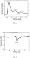
- Fig. 14 is a typical curve of a single waveform of the pulse wave measured by the piezoresistive electronic skin of the present invention. The result indicates that, the device not only achieves a quick and accurate real-time measurement of human pulse signals, but also may accurately distinguish P-peak, T-peak and D-peak in human pulse waves.
- pulse waves are relevant to information of heart rate, cardiac pulsation, blood viscosity and the like of human body. By accurate detection of the pulse waves, previous diagnosis of human diseases may be achieved.
- the use of the device for measuring pulse at wrist is one embodiment, and the device may also be used for real-time measuring arterial pulsation at other parts of the body, such as at neck, head and the like.
- the recognition of human speech may be achieved by measuring current signals in real-time when the voltage is at 2V.
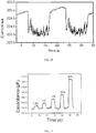
- the piezoresistive electronic skin when using the piezoresistive electronic skin to detect speech, the real-time I-t curve obtained when a subject says hello is shown in fig. 15 .
- the vibration of vocal cords may cause a vibration of skin, thereby resulting in that the resistance value of the device changes and the current flowed through the device also changes in the meantime. In this way, the relationship between speech and current is established.
- the waveforms of different speech and the changes thereof may be measured and obtained by the conversion of several physical quantities. Referring to fig.
- FIG. 16 it is another detection graph of speech recognition, with the use of a piezoresistive electronic skin of the present invention.
- the piezoresistive electronic skin when the piezoresistive electronic skin is put above a stereo without contact, the device vibrates in response to sound waves from the stereo. So the current value of the device changes. Besides, each type of sound vibration will have its own changing curve of current.
- the piezoresistive electronic skin of the present invention may be applied to the detection of tension.
- the deformation of the flexible piezoresistive electronic skin caused under the outside tension is precisely controlled by a high-precision stepping platform.
- the dielectric thickness, electrode area and the structure of the piezoresistive electronic skin change under the outside tension, and thus the resistance value of the electronic skin device changes.
- the electronic skin of the present invention may be applied on medical robot system and realizes functions of medical robot or surgery mechanical arm, touching, sensing and protecting human organ.
- the electronic skin includes the piezoresistive electronic skin.
- the piezoresistive electronic skin has same structure with the piezoresistive electronic skin according to embodiment 1.
- the piezoresistive electronic skin may be applied on the self-guide endoscopic medical system.
- FIG. 18 it is a signal acquisition graph of the endoscopic robot touching human internal organ, which is sensed by the electronic skin quickly, accurately and in real-time when the piezoresistive electronic skin of the present invention is applied on the endoscopic medical system.
- a sentient electronic skin device with high sensitivity, low energy consumption and high portability (wearable, attachable) may be formed, and new applications thereof, in various fields, may be researched and developed on the basis of physical characteristics of the piezoresistive electronic skin and the capacitive electronic skin.
- the piezoresistive electronic skin has high-sensitivity sensing of small applied force from the outside, and the capacitive electronic skin may be applied on attachable electronic device and system to realize the acquisition of speech information, human physiology signals and the like.
- the piezoresistive electronic skin and the ultrathin capacitive electronic device may be applied for achieving the real-time detection of human physiology signals (such as pulse, heart rate, breathing, blood pressure, and the like), and thereby achieving assessment of human health and previous diagnosis of diseases.
- human physiology signals such as pulse, heart rate, breathing, blood pressure, and the like
Landscapes
- Health & Medical Sciences (AREA)
- Life Sciences & Earth Sciences (AREA)
- Engineering & Computer Science (AREA)
- Surgery (AREA)
- Physics & Mathematics (AREA)
- Veterinary Medicine (AREA)
- Public Health (AREA)
- Biomedical Technology (AREA)
- Heart & Thoracic Surgery (AREA)
- Medical Informatics (AREA)
- Molecular Biology (AREA)
- General Health & Medical Sciences (AREA)
- Animal Behavior & Ethology (AREA)
- Biophysics (AREA)
- Pathology (AREA)
- Cardiology (AREA)
- Physiology (AREA)
- General Physics & Mathematics (AREA)
- Mechanical Engineering (AREA)
- Nuclear Medicine, Radiotherapy & Molecular Imaging (AREA)
- Theoretical Computer Science (AREA)
- General Engineering & Computer Science (AREA)
- Dentistry (AREA)
- Oral & Maxillofacial Surgery (AREA)
- Robotics (AREA)
- Human Computer Interaction (AREA)
- Audiology, Speech & Language Pathology (AREA)
- Optics & Photonics (AREA)
- Radiology & Medical Imaging (AREA)
- Pulmonology (AREA)
- Vascular Medicine (AREA)
- Ophthalmology & Optometry (AREA)
- Measurement And Recording Of Electrical Phenomena And Electrical Characteristics Of The Living Body (AREA)
- Measurement Of The Respiration, Hearing Ability, Form, And Blood Characteristics Of Living Organisms (AREA)
- Force Measurement Appropriate To Specific Purposes (AREA)
- Pressure Sensors (AREA)
- Laminated Bodies (AREA)
- Materials For Medical Uses (AREA)
- Measuring Pulse, Heart Rate, Blood Pressure Or Blood Flow (AREA)
Description
- The present invention relates to the field of sensors, more particularly to an electronic skin, a preparation method and a use thereof.
- As automatic devices with artificial intelligence, robots have been more and more involved in people's daily lives and have replaced human to perform related work in hazardous industries such as high temperature, high pressure, explosive disposal, etc. By the integration of various sensors, the existing robot systems already have achieved a lot of human sensations, like vision, hearing and olfaction. However, the robot systems are faced with one of the most challenging problems all the time: how to get sensitive tactile sensation like human beings. The birth of electronic skin will bring the robot systems tremendous changes and will enable the robots to get more information from the external environment.
- Since the University of Tokyo first suggested OFET electronic skin, some research groups in Japan and America have constructed the electronic skin based on organic field effect transistor, capacitive electronic skin as well as piezoresistive electronic skin successfully. However, the application ranges of these devices are limited due to complicated processing technic and device structures, bigger driving voltage, lower sensitivity or characteristics such as non- transparency and non-flexibility resulting from the use of rigid silicon-based materials. Therefore, it is necessary to provide an artificial electronic skin which has simple structure, high sensitivity, high accuracy and durability.
- Along with the advent of conceptual products such as Google glass, Apple Watch, and the like, wearable equipment comes to public attention with advantages such as high sensitivity, low cost, low power consumption, easy portability, more convenient user experience, and so on, extending functions that PC and cell phone do not have. By the deep integration with software and hardware technology and by means of highly integrated intelligent terminal, wearable equipment not only creates smart personal life, but also builds smart city and even smart world, thereby bringing the life-style and consumption concept of human being revolutionary changes. There will be many varieties of wearable equipment in future, but all of which will be combined with sensor technology, taking the human body as a part of input or output process, then connecting the Internet by itself or by APP on the cell phone, and finally achieving intelligent human-machine interaction.
- The electronic skin with nanostructure, ultrathin thickness, lighter weight, and flexibility similar to human skin is the most suitable material for constructing wearable equipment. Recently, the world-recognized top journal Nature has reported an ultrathin (2µm) electronic skin with OFET structure, which is lighter than feather and still works after being kneaded, stretched out, or drawn back. However, because of low carrier mobility of OFET, the electronic skin needs high working voltage and high power consumption, but has low sensitivity.
- In addition, with the rapid development of communication technology and continuous progress of computer science and technology, speech recognition becomes a remarkable high-tech intelligent human-computer interaction technology, which involves multi-disciplines comprehensive technologies of phonetics, vocalism principle, microelectronic technology, computer information processing technology, speech processing technology, circuit and system, sense technology, and so on. The application thereof has become a competitive new high-technology industry.
- The reported speech recognition technologies are usually based on methods of speech template, large vocabulary continuous speech recognition, acoustic model, etc. However, these traditional speech recognition technologies have lots of problems. For example, in circumstances of noisy environment, unclear pronunciation with accent or in dialect, or of a multitude of voices from multi-people at the same time, voice input will have a bad effect, low recognition rate and even will fail to be recognized. The main reason for these problems mentioned above is that traditional voice acquisition modules capture voices by collecting transmitted signals of voices in the air, while other acoustic sources around will interfere the collecting of voice data.
- Moreover, in order to extract physiological and pathological information from the pulse waves of human body as the basis for clinical diagnose and treatment, a number of pulse monitors appear in recent years, such as portable electronic sphygmomanometer which can measure pulse. However, this kind of portable electronic sphygmomanometers use mini air pump to pressurize rubber pneumatic bag and need pressurizing process and depressurizing process in every single measurement, thereby having some problems, such as big size, uncomfortable user experience during pressurization and depressurization, low accuracy in the detection of pulse, disability of displaying a full waveform of pulse wave, etc. Some large sphygmographes, such as Complior Analyse (France), have accurate measuring results and good repeatability, but are mainly used in specialist treatment and the study of epidemiology and are too expensive to use in household or popular portable medical services.
- Furthermore, in order to meet the growing needs of people, it is very necessary to explore new applications in various fields for the electronic skin which is an electronic device with extremely high sensitivity.
-
KR 20110042924A polymer layer 26 formed with carbonnanotube film patterns 25 is deformed and intrudes into the space of thespacer 31, and thus the resistance value changes. -
US 2010/050779A1 discloses a load cell, comprising: a block of carbon nanotubes; a first multiplicity of electrodes on a first side of said block; a second multiplicity of electrodes on an opposing side of said block to said first side, and an electrical circuit for measuring the electrical resistance, wherein the substrates 252 and 254 are fixed to the electrodes or the block of carbon nanotubes by adhesive material 256. -
KR 20130003856A Polymer cover 60, apolymer membrane 30 and asubstrate 10, wherein thesubstrate 10 is arranged with a plurality ofholes 20 or grooves, a plurality of grooves 32a, 34a are formed on twosides 32, 34 of thepolymer membrane 30 for receiving first andsecond electrode strips second electrode strips holes 20 and first and second metal electrodes 44, 54 at the other portions. -
US 2012/223454A1 discloses a mold and manufacturing method thereof. The mold has a pattern-formation surface 1A defined by onesurface 3, wherein the pattern-formation layer has a projection-and-depression structure area for patterning, and a base surface 4 defined by another surface. At least the pattern-formation layer and the base surface each comprise a polydimethylsiloxane layer. -
WO 2004/069736 A2 discloses a conductive article, including a substrate and a conductive layer that is formed on the surface of the substrate. - Additional state of the art is known from
EP 1480029 A2 andUS 201002958120A1 - One of the goals of the present invention is to provide a piezoresistive electronic skin with a completely new structure, which has advantages of low cost, low driving voltage, high sensitivity, short response time, high stability, etc.
- In order to achieve the above goal, the present invention provides a piezoresistive electronic skin according to
claim 1. - Preferably, at least one of the flexible substrates uses polydimethylsiloxane film, or, at least one of the flexible substrates is made of one or a combination of more of the follows: polyvinylidene fluoride (PVDF), polyvinyl fluoride (PVF), polyvinyl chloride (PVC), polyethylene (PE), polypropylene (PP), polystyrene (PS), polymethyl methacrylate (PMMA), polyvinyl chloride (PVC), nylon (Nylon), polycarbonate (PC), polyurethane (PU), polytetrafluoroethylene (PTFE), polyethylene terephthalate (PET, PETE), and high-polymer rubber materials.
- According to the invention, the flexible substrate uses polydimethylsiloxane film, at least one surface of the polydimethylsiloxane film which faces the other substrate is provided with patterns, the sizes of the patterns are between 0.1 and 500µm; and the unit amount of the patterns in a square centimeter is between 1 and 1012.
- The template is anyone of a silicon substrate provided with microstructure, a glass substrate provided with microstructure, a metallic substrate provided with microstructure, a plastic substrate, fabric or silk article provided with microstructure, and a bio-organ provided with microstructure.
- Furthermore, the conductive layer is attached with organic polymer material on the surfaces, wherein the organic polymer material is one or a combination of more of the follows: polyvinylidene fluoride (PVDF), polyvinyl fluoride (PVF), polyvinyl chloride (PVC), polyethylene (PE), polypropylene (PP), polystyrene (PS), polymethyl methacrylate (PMMA), polyvinyl chloride (PVC), nylon (Nylon), polycarbonate (PC), polyurethane (PU), polytetrafluoroethylene (PTFE), polyethylene terephthalate (PET, PETE), PDMS, and high-polymer rubber materials.
- In order to achieve the above goal, the present invention also provides a preparation method of the piezoresistive electronic skin according to
claim 10. - Compared with the existing technologies, the present invention has advantages as follows: the piezoresistive electronic skin uses carbon nanotube films as the conductive layers and uses materials, such as polydimethylsiloxane, polyethylene terephthalate, polyvinyl alcohol, polyvinyl formal, polyethylene, and so on, as the flexible substrates, allowing the substrate to be high flexible and pliable, and to have low operating voltage, little power consumption, as well as high sensitivity and short response time. Employing the patterned flexible substrate with the increased amount of contact resistances as the basis greatly improves the sensitivity of electronic skin reacting to tiny applied force from the outside. Meanwhile, the template used in the patterning process is a soft template, such as fabric, silk cloth, and the like, which has low-cost, is easy to get, and does not need any complex micromachining process, effectively improving the practicality of the technical solution, saving material resources and decreasing the manufacturing cost of the piezoresistive electronic skin.
- The present invention also provides a use of the piezoresistive electronic skin in detecting human pulse, cardiac pulsation, tension, breathing, intraocular pressure, vibration of muscle groups in the throat, speech recognition, muscle and skin movement caused by moving, blood pressure, and in medical robot, endoscopic robot system, surgery mechanical arm on the aspect of touching, sensing and protecting human organ. the problems of poor speech input effect and low recognition rate in the existing technology.
- In order to achieve the above goal, technical solutions are provided as follows:
- A speech recognition system is provided, which comprises:
- the above-mentioned piezoresistive electronic skin,
- a data processing module for receiving signals from the piezoresistive electronic skin and transmitting the processed signals to display module;
- a display module for receiving and displaying the signals from the data processing module.
- The present invention also provides a speech recognition method, comprising steps as follows:
- collecting vibration signals of vocal cords by means of the above-mentioned piezoresistive electronic skin; filtering and amplifying the collected vibration signals, and extracting characteristic signals;
- analyzing and recognizing the characteristic signals by time domain analysis method or frequency domain analysis method, and displaying the recognition results by means of a display module.
- Another goal of the present invention is to provide a pulse detection system and a method respectively on the basis of the piezoresistive electronic skin or the capacitive electronic skin so as to solve the existing technical problems of the pulse detection device, such as big size, high energy consumption, low accuracy, high cost, disability of displaying a full waveform of pulse wave, etc.
- In order to achieve the above goal, technical solutions are provided as follows:
- A pulse detection system is provided, comprising:
- the piezoresistive electronic skin according to the one of
embodiment 1; a filter circuit for filtering the signals received from the piezoresistive electronic skin to obtain valid pulse signals; - an amplification circuit for amplifying the valid pulse signals and transmitting them to an analog-to-digital conversion circuit;
- a display device for receiving and displaying the signals received from the analog-to-digital conversion circuit.
- the piezoresistive electronic skin according to the one of
- Preferably, the analog-to-digital conversion circuit communicates with the display device by Bluetooth, Zigbee or Wifi.
- A pulse detection method is also provided, comprising steps as follows:
- collecting pulse signals by means of the above-mentioned piezoresistive electronic skin; filtering the collected pulse signals to obtain valid pulse signals;
- amplifying the valid pulse signals and transmitting them to an analog-to-digital conversion circuit;
- displaying the signals received from the analog-to-digital conversion circuit by means of a displayer.
- Compared with the existing technologies, the present invention has advantages as follows:
- By incorporating new micro-nano sensing technology and using the ultrathin, elastic film material which is non-toxic and has good biocompatibility, the piezoresistive electronic skin or the capacitive electronic skin can be well adhered to human skin to form a wearable device and provide excellent user experience. In the meantime, due to the distinctive nanostructure of the sensitive material, the device has high sensitivity, good stability and portability with light weight and small size as well as low cost. Furthermore, the speech recognition system and method obtained on the basis of the above-mentioned piezoresistive electronic skin or the capacitive electronic skin solve the existing technical problems of poor speech detection effect and low recognition rate, having property of synchronized reorganization, high recognition rate, small size and being convenient to carry. Moreover, the pulse detection system and method obtained on the basis of the piezoresistive electronic skin or the capacitive electronic skin solve the existing problems, such as big size, uncomfortable
-
-
Fig. 1 is a schematic diagram of a piezoresistive electronic skin according to a preferred embodiment of the present invention; -
Fig. 2 is a flow diagram of a preparation method of an electronic skin according to an embodiment of the present invention; -
Fig. 3 is a SEM image of a polydimethylsiloxane film provided with micropattern according to an embodiment of the invention; -
Fig. 4 is a SEM image of a single-walled carbon nanotube film according to an embodiment of the invention; -
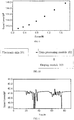
Fig. 5 is a plot of resistance versus the change of pressure using an electronic skin according to an embodiment of the present invention; -
Fig. 6 is a schematic diagram of a capacitive electronic skin according to an embodiment of the present invention; -
Fig. 7 is a SEM image of a silicon wafer template according to an embodiment of the present invention; -
Fig. 8 is a SEM image of a flexible PDMS film molded from the template corresponding tofigure 7 ; -
Fig. 9 is a plot of the response of a capacitive electronic skin versus applied force not falling under the scope of the invention; -
Fig. 10 is a schematic diagram of a speech recognition system according to an embodiment of the present invention; -
Fig. 11 is a plot showing the detection results of speech recognition with the use of a capacitive electronic skin not falling under the scope of the invention; -
Fig. 12 is a schematic diagram of a pulse detection system according to an embodiment of the present invention; -
Fig. 13 is a oscillogram of a wrist pulse wave measured by a piezoresistive electronic skin according to an embodiment of the present invention; -
Fig. 14 is a oscillogram of an individual pulse waveform measured by a piezoresistive electronic skin according to an embodiment of the present invention; -
Fig. 15 is a first detection graph of speech recognition, with the use of a piezoresistive electronic skin according to an embodiment of the present invention; -
Fig. 16 is a second detection graph of speech recognition, with the use of a piezoresistive electronic skin according to an embodiment of the present invention; -
Fig. 17 is a response diagram of a capacitive electronic skin detecting external tension not falling under the scope of the invention; -
Fig. 18 is a force-signal acquisition graph of a piezoresistive electronic skin applied on the endoscopic medical system according to an embodiment of the invention. - The present invention will be further explained below in detail with reference to figures and particular embodiments.
- This embodiment provides a piezoresistive electronic skin, comprising: a plurality of overlapped flexible substrates; a conductive layer arranged on contact surface of adjacent flexible substrates, at least one contact area of the conductive layer has non-planar structure; and conductive electrodes electrically connected with the conductive layer.
- Referring to
fig. 1 , as an embodiment, the electronic skin comprises twoflexible substrates conductive layers flexible substrates conductive layers conductive electrodes conductive layers - In specific implementations, each of the flexible substrates is made of various materials.
- According to the invention at least one of the flexible substrates uses a polydimethylsiloxane film, at least one surface of the polydimethylsiloxane film is provided with micro-nano patterns, the sizes of the patterns are between 0.1 and 500µm; and the unit amount of the patterns in a square centimeter is between 1 and 1012. In another embodiment, at least one of the flexible substrates is made of one or a combination of more of the follows: polyvinylidene fluoride (PVDF), polyvinyl fluoride (PVF), polyvinyl chloride (PVC), polyethylene (PE), polypropylene (PP), polystyrene (PS), polymethyl methacrylate (PMMA), polyvinyl chloride (PVC), nylon (Nylon), polycarbonate (PC), polyurethane (PU), polytetrafluoroethylene (PTFE), polyethylene terephthalate (PET, PETE), and high-polymer rubber materials.
- In the present embodiment, the patterns are preferably formed by coating the polydimethylsiloxane onto a template and solidifying it. Particularly, for example, degassing it in vacuum for 1-30 minutes and coating it onto a template. The template is preferably anyone of a silicon substrate provided with microstructure, a glass substrate provided with microstructure, a metallic substrate provided with microstructure, a plastic substrate, fabric or silk article provided with microstructure, and a bio-organ provided with microstructure. In specific implementations, making a template by material which is easy to get will effectively improve the practicality of the piezoresistive electronic skin and greatly decrease the manufacturing cost of the piezoresistive electronic skin.
- The
conductive layers - The carbon nanotube film may also be a carbon nanotube film mixed or modified by nitrogen or boron, precious metal, metal, surface active agent, organic macromolecule compound, and so on. The carbon nanotubes may be carbon nanotubes functionalized by hydroxy (-OH), carboxyl (-COOH), amidogen (-NH2), by high molecular polymer, by metal nanoparticle, by metallic oxide, or by biomolecule.
- The
conductive layers - In another embodiment, the conductive layer is attached with organic polymer material on the surface.
- Furthermore, analogized with the material of the flexible substrates, the organic polymer material is preferably likewise one or a combination of more of the follows: polyvinylidene fluoride (PVDF), polyvinyl fluoride (PVF), polyvinyl chloride (PVC), polyethylene (PE), polypropylene (PP), polystyrene (PS), polymethyl methacrylate (PMMA), polyvinyl chloride (PVC), nylon (Nylon), polycarbonate (PC), polyurethane (PU), polytetrafluoroethylene (PTFE), polyethylene terephthalate (PET, PETE), PDMS, and high-polymer rubber materials. Thereinto, the high-polymer rubber materials include, but are not limited to, butyl rubber, cis-polybutadiene rubber, chloroprene rubber, ethylene propylene diene monomer rubber, acrylate rubber, and polyurethane rubber. In the present embodiment, the sensitivity and stability of the conductive layer can be increased by adhering different materials to the surface of the conductive layer.
- Preferably, in one embodiment, a layer of PVDF piezoelectric material (not limited to PVDF) may be added between the conductive film layers 21, 22 shown in
fig. 1 , so as to improve the sensitivity and stability of the device. - In the embodiment as shown in
fig. 1 , theconductive electrode 31 is connected with theconductive layer 21 but is not connected with theconductive layer 22, while theconductive electrode 32 is connected with theconductive layer 22 but is not connected with theconductive layer 21, and the thin film of carbon tubes provided with micro-nano patterns can only be connected with one of the conductive electrodes, respectively. Moreover, theconductive electrodes - In the present embodiment, the way the two layers of patterned conductive films are assembled, that is, the way the device is packaged, makes a big impact on the stability of the device. Thereinto, in one embodiment, the device is packaged by adhering the two layers of films from periphery and surroundings to form a stable quasi-single layer structure.
- Referring to
fig. 2 , the present invention also provides a preparation method of the piezoresistive electronic skin, the steps are as follows: -
S 1. Preparing two patterned flexible substrates, at least one layer of which is polydimethylsiloxane film. - In the step S1, the polydimethylsiloxane film is prepared by the following method, comprising a step S11 and a step S12:
- S11. Degassing polydimethylsiloxane in vacuum for 1-30 minutes and coating it onto a template provided with patterns, wherein the polydimethylsiloxane has a thickness of 0.1mm to 3mm, and then heating it for more than 0.5 hour at a temperature of 50 to 100 to solidify and mold it;
- S12. Removing the solidified and molded polydimethylsiloxane from the template by ultrasound in organic solvent for 5 to 30 minutes.
- In specific implementations, the template may be anyone of a silicon substrate, a glass substrate, a metallic substrate, a plastic substrate, fabric, silk article, each of which has microstructure, and a bio-organ provided with microstructure. The organic solvent may be methanol, ethyl alcohol or ethylene glycol. One or two surfaces of the prepared polydimethylsiloxane film are placed in the oxygen plasma condition to react for 1 to 60 minutes. The polydimethylsiloxane film may also be high molecular materials, including but not limited to one or a combination of more of the follows: polyvinylidene fluoride (PVDF), polyvinyl fluoride (PVF), polyvinyl chloride (PVC), polyethylene (PE), polypropylene (PP), polystyrene (PS), polymethyl methacrylate (PMMA), polyvinyl chloride (PVC), nylon (Nylon), polycarbonate (PC), polyurethane (PU), polytetrafluoroethylene (PTFE), polyethylene terephthalate (PET, PETE), PDMS, and high-polymer rubber materials. Thereinto, the high-polymer rubber materials include, but are not limited to, butyl rubber, cis-polybutadiene rubber, chloroprene rubber, ethylene propylene diene monomer rubber, acrylate rubber, and polyurethane rubber.
- In the present embodiment, the density of the microstructure is (X*Y) lines/cm2, wherein 1<X<106, 1<Y<106. Thereinto, the density of the microstructure is defined as a density in a unit area of a square centimeter. The high-density structure refers to a structure with a density more than 44*77 lines/cm2, while the low-density structure refers to a structure with a density less than 27*38 lines/cm2. In the embodiment, the preferred density is 44*77 lines/cm2. In theory, the higher density, the higher sensitivity.
- In the present embodiment, with the use of the microstructure, the piezoresistive electronic skin has good output capability, wherein the sensitivity may reach up to 1.8KPa-1, the lower limit of detection may reach to 0.6Pa, and the response time may reach to 10ms. Referring to
fig. 3 , it is a scanning electron microscope (SEM) image of the prepared polydimethylsiloxane film provided with micro-nano pattern, showing that the polydimethylsiloxane film is formed with periodic microstructure patterns thereon. - S2. Preparing a solution for the conductive layer. In one embodiment, the solution for the conductive layer is a solution of carbon nanotubes, and the conductive layer is preferably a carbon nanotube film. Coating it to the patterned surfaces of the two flexible substrates to form carbon nanotube films, respectively. Assembling the carbon nanotube films by making the patterned surfaces face to face to form a film device with carbon nanotube films being contacted with each other.
- The step S2 may particularly comprise steps S21- S23:
- S21. Adding single-walled carbon nanotubes and/or double-walled carbon nanotubes, few-walled carbon nanotubes, multi-walled carbon nanotubes into an aqueous solution containing 1wt%-10wt% of surfactant until the concentration of carbon nanotubes reaches to 0.01-50mg/ml, then, pre-dispersing the mixed solution by ultrasound for 1min-10h to form carbon nanotube dispersion solution. In the present embodiment, the surfactant may be common ionic surfactant or non-ionic surfactant, preferably is ionic surfactant, more preferably, but is not limited to, sodium dodecylsulphate, sodium dodecyl benzene sulfonate and so on, with a preferred concentration of 1-10wt%.
- S22. Centrifuging the carbon nanotube dispersion solution at a speed of 1000-20000rpm for more than 0.1h, and taking the supernatant as pre-filmed solution.
- S23. Diluting the pre-filmed solution for 1-100 times by deionized water, and then evenly spraying the diluted solution of carbon nanotubes to the patterned surfaces of the two flexible substrates by sprayer to form carbon nanotube films. Assembling the carbon nanotube films by making the patterned surfaces face to face to form a film device with carbon nanotube films being contacted with each other. It should be explained that, the thickness and the electrical conductivity of the carbon nanotube film depend on the amount of carbon nanotubes contained therein and the time of spraying. The more content of carbon nanotubes and time of spraying, the better strength and electrical conductivity. In the present embodiment, the film-forming process may be performed in common film-forming manners, such as by vacuum filtration or spin coating, spray coating, printing, etc. For example, if the film is formed by spray coating, the process is as follows in detail: spraying the diluted carbon nanotube dispersion solution to the patterned polydimethylsiloxane film at a pressure of 0.1-1psi by sprayer, and then putting the film in heating furnace and heating it to 80-120°C to speed up the evaporation of water, after that, washing off the residual surfactant in the carbon nanotube film by deionized water so as to form a carbon nanotube film coated on the patterned polydimethylsiloxane film. If the film is formed by printing, coating and so on, the process is as follows in detail: coating the diluted carbon nanotube dispersion solution, by spin coating, spray coating and so on, to the material having flat surface, such as glass, mica, silicon wafer, and the like, so as to form a film. Accordingly, a method for removing the base is as follows: steeping it in water or aqueous solution containing acid, alkali, salt and so on until the carbon nanotube film falls off from the base, then shifting the carbon nanotube film onto the patterned polydimethylsiloxane film.
- Furthermore, before the assembling of the film device, step S23 comprises steeping the film which has the carbon nanotube film on the surface for several times by deionized water so as to remove the surfactant, disposing the carbon nanotube film in strong acid with a concentration of 3-8M for 0.1-24h after drying it. In the present embodiment, the strong acid may be anyone or a combination of nitric acid and hydrochloric acid.
- Referring to
fig. 4 , it is a SEM image with single-walled carbon nanotubes affixed to the polydimethylsiloxane film, showing that single-walled carbon nanotubes are cross-linked with each other and are affixed to the surface of the polydimethylsiloxane film. - S3. Forming upper, lower conductive electrodes respectively on the two carbon nanotube films by conductive material and leading wires from the conductive electrodes, thereby obtaining a piezoresistive electronic skin.
- In the step S3, the conductive materials for electrodes may be silver paste or fulmargin, or may be gas electrode such as gold, silver, copper, aluminum, or the like, which is made by steaming, ion sputtering and so on.
- Referring to
fig. 5 , at an operating voltage of 1V and in air atmosphere, the resistance value of the piezoresistive sensor is measured as 110-120kΩ. At time points of 30 seconds, 60 seconds, 90 seconds, the resistance values are decreased fast when pressures of 60Pa, 120Pa and 180Pa are accordingly applied respectively. For example, when a pressure of 60Pa is applied, the resistance value is rapidly decreased to 95-105kΩ. The result indicates that the piezoresistive sensor has high sensitivity and very short response time. - Compared with the existing technologies, the present invention has advantages as follows: the piezoresistive electronic skin uses carbon nanotube film as the conductive layer and uses materials, such as polydimethylsiloxane, polyethylene terephthalate, polyvinyl alcohol, polyvinyl formal, polyethylene, and so on, as the flexible substrates, enabling the substrate has advantages of high flexibility and being pliable, and it needs low operating voltage and little power consumption, but has high sensitivity and short response time. Moreover, the electronic skin uses the micro-patterned flexible substrate as the basis, with increased amount of contact resistances and obtains improved sensitivity to tiny applied force from the outside. Meanwhile, the template used in the patterning process is a soft template, such as fabric, silk cloth, and the like, which has low-cost and is easy to get, does not need any complex micromachining process, effectively improving the practicality of the piezoresistive electronic skin and greatly decreasing the manufacturing cost of the piezoresistive electronic skin.
- The international competition of information industry has been shown increasingly as the battle over science and technology. The speech recognition industry, as a strategic, forward-looking and important technology industry, has been the focus of scientific community and the industrial community. One embodiment of the present invention provides a new speech recognition technology and the relevant device. A simple, feasible and systematic method for recognizing vibration signals is also provided, comprising the steps as follows: collecting vibration signals generated by vocal cords during speaking by means of micro/nano sensor instead of collecting transmitted sound signals of voices in the air by means of acquisition module in traditional speech recognition technology, pre-treating the vibration signals, such as amplifying the vibration signals, filtering the vibration signals and the like, extracting characteristic signals, recognizing and analyzing by time domain analysis, frequency domain analysis and the like, and finally displaying the results.
- This embodiment makes innovations on the basis of traditional speech recognition technology, mainly focused on the method for collecting speech signals and on the extracting device. It has advantages of synchronized recognition, high recognition rate, small size and being convenient to carry. In the meantime, due to the use of flexible thin film material, it's convenient to construct the present device as wearable equipment.
- As shown in
fig. 10 , in an embodiment of the present invention, a speech recognition system comprises anelectronic skin 101, adata processing module 102 and adisplay module 103. Theelectronic skin 101 includes piezoresistive electronic skin and capacitive electronic skin. - In this embodiment, the piezoresistive electronic skin is used for collecting vibration signals of vocal cords, the
data processing module 102 is used for filtering and amplifying the collected vibration signals, extracting characteristic signals, analyzing and recognizing the characteristic signals by time domain analysis method or frequency domain analysis method, and thedisplay module 103 is used for displaying the recognition results. - In one embodiment, the piezoresistive electronic skin may be the piezoresistive electronic skin provided in the
above embodiment 1, the detail structure of which refers toembodiment 1 and need not be repeated here. - In addition, the preparation method of the piezoresistive electronic skin may take the preparation method of the piezoresistive electronic skin provided in the
above embodiment 2 for reference. - Another embodiment of the present invention provides a speech recognition method, comprising:
- Collecting vibration signals of vocal cords by means of the piezoresistive electronic skin according to
embodiment 1; Filtering and amplifying the collected vibration signals, and extracting characteristic signals; - Analyzing and recognizing the characteristic signals by time domain analysis method or frequency domain analysis method, and displaying the recognition results by means of a display module.
- In an embodiment, the speech recognition method provided in the present embodiment may use the speech recognition system according to
embodiment 3 to detect signals. Due to the high sensitivity of the piezoresistive electronic skin and the portability of the speech recognition system, the speech recognition method is feasible, practicable and efficient. - Referring to
fig. 12 , an embodiment of the present invention provides a pulse detection system. - The pulse detection system comprises an
electronic skin 201, afilter circuit 202, anamplification circuit 203, an analog-to-digital conversion circuit 204 and adisplay device 205. In the present embodiment, theelectronic skin 201 includes piezoresistive electronic skin. - Thereinto, the electronic skin in the present embodiment may be the piezoresistive electronic skin provided in
embodiment 1 the detail structures thereof refer to the above embodiments, and need not be repeated here. - Pulse is formed by the flow of the blood shot into aorta by ventricle and flowed along the arterial system from aorta root in the form of waves during the periodic expansion and contraction of the heart. When the above wearable pulse detection device is put on the area with aterial pulse, the signals of pulse pulsation with good integrality, small distortion, stable baseline and moderate amplitude are automatically collected by the piezoresistive electronic skin, then the pulse signals output by the electronic skin are filtered out the background noise signals by means of the
filter circuit 202 to get valid pulse wave signals, then the signals are amplified by amplifying circuit and transmitted to ADC circuit 203 (further comprises an analog-to-digital conversion circuit) to be switched, after that, the signals are transmitted to the receiving device on thedisplay device 205 by wireless Bluetooth transmitting technology, Zigbee technology or Wifi technology, and finally the pulse waves are displayed on the displayer in real-time. - The analog-to-
digital conversion circuit 204 and thedisplay device 205 may communicate by GPRS (General Packet Radio Service), GSM (Global System of Mobile communication), WLAN (Wireless Local Area Networks), CDMA (Code Division Multiple Access), TDMA (Time Division Multiple Access), TV communication network, Zigbee technology or Wifi technology, or other telecommunication networks. Obviously, the analog-to-digital conversion circuit 204 and thedisplay device 205 may also be connected in a wired manner. - In addition, the preparation method for the above piezoresistive electronic skin may refer to the preparation method for the piezoresistive electronic skin provided in the above embodiment.
- The pulse detection system provided in the present embodiment has advantages as follows: as the result of using the above piezoresistive electronic skin, it has advantages of toxic free and good biocompatibility. So it can be adhered to human skin and bring the user excellent experience. In the meantime, due to the distinctive nanostructure of sensitive materials of electronic skin, the pulse detection system has high sensitivity and good stability, has portability as being light, small and flexible on the whole, and has low cost in fabrication, and thus it has good practicability.
- An embodiment of the present invention provides a pulse detection method as follows:
- Collecting pulse signals by means of the piezoresistive electronic skin according to the
embodiment 1; Filtering the collected pulse signals to get valid pulse signals; - Amplifying the valid pulse signals and transmitting them to an analog-to-digital conversion circuit;
- Displaying the signals received from the analog-to-digital conversion circuit by means of a displayer.
- In this embodiment, the pulse detection system according to
embodiment 7 is used to detect pulse signals. When the device is put on the pulse, sensor capacitance changes with the beat of pulse. Then, filtering out the background noise signals by means of a filter circuit to get valid pulse wave signals, amplifying the signals by amplifying circuit and transmitting them to ADC circuit to be switched, transmitting the signals to a receiving device on a displayer by wireless Bluetooth transmitting technology, thereby displaying the pulse waves on the displayer in real-time. - An embodiment of the present invention provides multiple new uses of the electronic skin in a variety of fields.
- The electronic skin provided in the present invention may be used for detecting human physiology signals comprising arterial pulsation, cardiac pulsation, tension detection, intraocular pressure, vibration of muscle groups in the throat caused by talking, speech recognition caused by contact and non-contact vibration, muscle and skin movement of other parts of the body caused by moving. For example, when detecting arterial pulsation at wrist, P-peak, T-peak and D-peak in the pulse can be accurately recognized. The arterial pulsation comprises the pulse in each part of the body beating with the arterial pulsation. Furthermore, the electronic skin has potential applications on the aspect of touching, sensing and protecting human organ, in respects such as blood pressure, breathing, medical robot, endoscopic robot system, surgery mechanical arm, etc.
- In the present embodiment, the electronic skin comprises: the piezoresistive electronic skin according to
embodiment 1. - New uses of the piezoresistive electronic skin, in a variety of fields, provided by the present invention are explained by four particular embodiments as follows.
- Putting the prepared piezoresistive/capacitive electronic skin on the wrist, the detection of human pulse signals can be achieved by measuring current signals in real-time when the voltage is at 2V. Particularly, when using the piezoresistive electronic skin to detect an individual pulse wave, the oscillogram of wrist pulse measured by the piezoresistive electronic skin is shown in
fig. 13 .Fig. 14 is a typical curve of a single waveform of the pulse wave measured by the piezoresistive electronic skin of the present invention. The result indicates that, the device not only achieves a quick and accurate real-time measurement of human pulse signals, but also may accurately distinguish P-peak, T-peak and D-peak in human pulse waves. Theses pulse waves are relevant to information of heart rate, cardiac pulsation, blood viscosity and the like of human body. By accurate detection of the pulse waves, previous diagnosis of human diseases may be achieved. The use of the device for measuring pulse at wrist is one embodiment, and the device may also be used for real-time measuring arterial pulsation at other parts of the body, such as at neck, head and the like. - Putting the prepared piezoresistive electronic skin on neck, the recognition of human speech may be achieved by measuring current signals in real-time when the voltage is at 2V. In one embodiment , when using the piezoresistive electronic skin to detect speech, the real-time I-t curve obtained when a subject says hello is shown in
fig. 15 . When the subject talks, the vibration of vocal cords may cause a vibration of skin, thereby resulting in that the resistance value of the device changes and the current flowed through the device also changes in the meantime. In this way, the relationship between speech and current is established. The waveforms of different speech and the changes thereof may be measured and obtained by the conversion of several physical quantities. Referring tofig. 16 , it is another detection graph of speech recognition, with the use of a piezoresistive electronic skin of the present invention. As shown infig. 16 , when the piezoresistive electronic skin is put above a stereo without contact, the device vibrates in response to sound waves from the stereo. So the current value of the device changes. Besides, each type of sound vibration will have its own changing curve of current. - The piezoresistive electronic skin of the present invention may be applied to the detection of tension. In specific implementations, when the prepared piezoresistive electronic skin is applied to the detection of tension, the deformation of the flexible piezoresistive electronic skin caused under the outside tension is precisely controlled by a high-precision stepping platform. The dielectric thickness, electrode area and the structure of the piezoresistive electronic skin change under the outside tension, and thus the resistance value of the electronic skin device changes.
- The electronic skin of the present invention may be applied on medical robot system and realizes functions of medical robot or surgery mechanical arm, touching, sensing and protecting human organ. Thereinto, the electronic skin includes the piezoresistive electronic skin. Thereinto, the piezoresistive electronic skin has same structure with the piezoresistive electronic skin according to
embodiment 1. - For example, applying the piezoresistive electronic skin to endoscopic robot and enabling the endoscopic robot to have ability to detect small applied force from outside. When performing endoscopic operation, the endoscopic robot system may obtain the touching signal of the human internal organ and input the information into the control center of the endoscopic robot system, and then the control center may adjust the postures and movements of the robot, reducing the pain of the patient and the damage for the human internal organ. In one embodiment, the piezoresistive electronic skin of the present invention may be applied on the self-guide endoscopic medical system.
- Referring to
fig. 18 , it is a signal acquisition graph of the endoscopic robot touching human internal organ, which is sensed by the electronic skin quickly, accurately and in real-time when the piezoresistive electronic skin of the present invention is applied on the endoscopic medical system. - When implementing the embodiments of the invention, by the combination of nanostructure and new type nano-material, a sentient electronic skin device with high sensitivity, low energy consumption and high portability (wearable, attachable) may be formed, and new applications thereof, in various fields, may be researched and developed on the basis of physical characteristics of the piezoresistive electronic skin and the capacitive electronic skin. Thereinto, in the respect of sensing information from outside, the piezoresistive electronic skin has high-sensitivity sensing of small applied force from the outside, and the capacitive electronic skin may be applied on attachable electronic device and system to realize the acquisition of speech information, human physiology signals and the like. Therefore, the piezoresistive electronic skin and the ultrathin capacitive electronic device may be applied for achieving the real-time detection of human physiology signals (such as pulse, heart rate, breathing, blood pressure, and the like), and thereby achieving assessment of human health and previous diagnosis of diseases.
Claims (13)
- A piezoresistive electronic skin, comprising two overlapping flexible substrates (11; 12); conductive layers (21; 22) arranged on contact surfaces of adjacent flexible substrates (11; 12); and
conductive electrodes (31; 32) electrically connected with said conductive layers (21; 22),
characterized in that:at least one flexible substrate is a polydimethylsiloxane film, and at least one surface of said polydimethylsiloxane film which faces the other flexible substrate (11; 12) is provided with micro-nano patterns, the sizes of said patterns are between 0.1 and 500µm, and the unit amount of said patterns in a square centimeter is between 1 and 1012,wherein said conductive layers (21; 22) are coated on patterned contact surface of adjacent flexible substrates (11; 12) and being contacted with each other,wherein said conductive layers are micro-nano patterned carbon nanotube films. - The piezoresistive electronic skin according to claim 1, characterized in that at least one of said flexible substrates (11; 12) is made of one or a combination of more of the following materials: polydimethylsiloxane (PDMS) film, polyvinylidene fluoride (PVDF), polyvinyl fluoride (PVF), polyvinyl chloride (PVC), polyethylene (PE), polypropylene (PP), polystyrene (PS), polymethyl methacrylate (PMMA), nylon (Nylon), polycarbonate (PC), polyurethane (PU), polytetrafluoroethylene (PTFE), polyethylene terephthalate (PET, PETE), and high-polymer rubber materials.
- The piezoresistive electronic skin according to claim 2, characterized in that said patterns are formed from said polydimethylsiloxane which is solidified after being coated onto a template,
said template is anyone of a silicon substrate provided with microstructure, a glass substrate provided with microstructure, a metallic substrate provided with microstructure, a plastic substrate, fabric or silk article provided with microstructure, and a bio-organ provided with microstructure. - The piezoresistive electronic skin according to claim 1, characterized in that said conductive layer (21; 22) comprises networks formed by cross-linked carbon nanotubes.
- The piezoresistive electronic skin according to claim 4, characterized in that the light transmittance of said carbon nanotube film is between 50% and 97%, and the sheet resistance is between 102Ω/sq and 107Ω/sq.
- The piezoresistive electronic skin according to claim 5, characterized in that the thickness of said carbon nanotube film is between 10nm and 500nm, said carbon nanotube film is made of one type or a combination of more types of single-walled carbon nanotubes, double-walled carbon nanotubes and multi-walled carbon nanotubes, wherein said single-walled carbon nanotubes are metallic single-walled carbon nanotubes, semiconductor-type carbon nanotubes or hybrid single-walled carbon nanotubes containing both metallic single-walled carbon nanotubes and semiconductor-type carbon nanotubes.
- The piezoresistive electronic skin according to claim 1, characterized in that said conductive layer (21; 22) is made of one or a combination of more of any conductive metal among copper, silver and gold, and semiconductor materials.
- The piezoresistive electronic skin according to anyone of claims 1-7, characterized in that said conductive layer (21; 22) is attached with organic polymer material on the surfaces, said organic polymer material is one or a combination of more of materials as follows: polyvinylidene fluoride (PVDF), polyvinyl fluoride (PVF), polyvinyl chloride (PVC), polyethylene (PE), polypropylene (PP), polystyrene (PS), polymethyl methacrylate (PMMA), nylon (Nylon), polycarbonate (PC), polyurethane (PU), polytetrafluoroethylene (PTFE), polyethylene terephthalate (PET, PETE), polydimethylsiloxane(PDMS), and high-polymer rubber materials.
- The piezoresistive electronic skin according to claim 1, characterized in that said conductive electrodes (31; 32) are made of one or a combination of more materials of gold, platinum, nickel, silver, indium, copper, carbon nanotube and graphene.
- A preparation method of the piezoresistive electronic skin according to one of claims 1-9, comprising steps as follows:S1. preparing the substrates (11; 12);S2. forming the conductive layers (21; 22) on said substrates (11; 12);S3. forming upper, lower conductive electrodes (31; 32) respectively on the two conductive layers (21; 22) by conductive material, and leading the wires from the conductive electrodes (31; 32), thereby obtaining the piezoresistive electronic skin,characterized in that:in step S 1, preparing the two patterned flexible substrates (11; 12), andin step S2, forming thepatterned conductive layers (21; 22) on the flexible substrates (11; 12) by preparing a solution for the conductive layer and respectively coating it to the patterned surfaces of the two flexible substrates (11; 12), and then assembling the two conductive layers (21; 22) by making the patterned surfaces face to face to form a film device with the patterned conductive layers (21; 22) being contacted with each other.
- The preparation method of the piezoresistive electronic skin according to claim 10, characterized in that said flexible substrates (11; 12) in said step S1 are prepared by steps as follows:S11. degassing the polydimethylsiloxane in vacuum for 1-30 minutes and coating it onto a template provided with patterns, wherein the polydimethylsiloxane has a thickness of 0.1mm to 3mm, and then heating it for more than 0.5 hour at a temperature of 50°C to 100°C to solidify and mold it;S12. removing the solidified and molded polydimethylsiloxane from the template by ultrasound in organic solvent for 5 to 30 minutes.
- The preparation method of the piezoresistive electronic skin according to claim 11, characterized in that said template is chosen from a silicon substrate provided with microstructure, a glass substrate provided with microstructure, a metallic substrate provided with microstructure, a plastic substrate, fabric or silk article provided with microstructure, and a bio-organ provided with microstructure; said organic solvent may be methanol, ethyl alcohol and ethylene glycol.
- A use of the piezoresistive electronic skin according to anyone of claims 1-9 in detecting human pulse, cardiac pulsation, tension, breathing, intraocular pressure, vibration of muscle groups in the throat, speech recognition, muscle and skin movement caused by moving, blood pressure, and in medical robot, endoscopic robot system, surgery mechanical arm on the aspect of touching, sensing and protecting human organ.
Applications Claiming Priority (5)
| Application Number | Priority Date | Filing Date | Title |
|---|---|---|---|
| CN2013100344781A CN103083007A (en) | 2013-01-29 | 2013-01-29 | Piezoresistive electronic skin and preparation method thereof |
| CN201310507497.1A CN104555883A (en) | 2013-10-24 | 2013-10-24 | Electronic skin and production method thereof |
| CN201310508179.7A CN104575500B (en) | 2013-10-24 | 2013-10-24 | Application, speech recognition system and method for the electronic skin in speech recognition |
| CN201310693411.9A CN104706335B (en) | 2013-12-17 | 2013-12-17 | Application of the electronic skin in pulse detection, pulse detection system and method |
| PCT/CN2014/071631 WO2014117724A1 (en) | 2013-01-29 | 2014-01-28 | Electronic skin, preparation method and use thereof |
Publications (3)
| Publication Number | Publication Date |
|---|---|
| EP2953012A1 EP2953012A1 (en) | 2015-12-09 |
| EP2953012A4 EP2953012A4 (en) | 2016-01-20 |
| EP2953012B1 true EP2953012B1 (en) | 2018-04-18 |
Family
ID=51261470
Family Applications (1)
| Application Number | Title | Priority Date | Filing Date |
|---|---|---|---|
| EP14746641.1A Active EP2953012B1 (en) | 2013-01-29 | 2014-01-28 | Electronic skin, preparation method and use thereof |
Country Status (7)
| Country | Link |
|---|---|
| US (1) | US9816882B2 (en) |
| EP (1) | EP2953012B1 (en) |
| JP (1) | JP6180547B2 (en) |
| KR (1) | KR101877108B1 (en) |
| AU (1) | AU2014211862B2 (en) |
| CA (1) | CA2899676C (en) |
| WO (1) | WO2014117724A1 (en) |
Families Citing this family (46)
| Publication number | Priority date | Publication date | Assignee | Title |
|---|---|---|---|---|
| US9494474B2 (en) | 2013-04-03 | 2016-11-15 | Texavie Technologies Inc. | Core-shell nanofiber textiles for strain sensing, and methods of their manufacture |
| KR20160091364A (en) * | 2013-11-28 | 2016-08-02 | 반도 카가쿠 가부시키가이샤 | Stretchable electrode, sensor sheet and capacitive sensor |
| CN105361977B (en) * | 2014-08-26 | 2018-08-10 | 中国科学院苏州纳米技术与纳米仿生研究所 | Resistance-type flexible and transparent joint part electronic skin and its preparation method and application |
| CN106153178A (en) * | 2015-03-17 | 2016-11-23 | 中国科学院苏州纳米技术与纳米仿生研究所 | Compliant conductive vibrating diaphragm, flexible vibration sensor and its preparation method and application |
| CN104803339A (en) * | 2015-04-21 | 2015-07-29 | 电子科技大学 | Flexible micro pressure sensor and preparation method thereof |
| WO2017020082A1 (en) * | 2015-08-03 | 2017-02-09 | Newsouth Innovations Pty Limited | Nanocomposite as stress sensor |
| US20170061824A1 (en) * | 2015-09-01 | 2017-03-02 | Pepe Loves Books, Inc. | Bilingual blocks, application, and system |
| KR101790558B1 (en) * | 2015-09-07 | 2017-10-27 | 울산과학기술원 | Artificial electronic skin based on ferroelectric composites |
| US20170086704A1 (en) * | 2015-09-25 | 2017-03-30 | Intel Corporation | Electronic skin |
| CN108368469A (en) * | 2015-10-07 | 2018-08-03 | 加利福尼亚大学校董会 | Graphene based multimodal sensor |
| CA3002455C (en) * | 2015-11-09 | 2024-02-13 | Shiseido Americas Corporation | Compositions and methods for application over skin |
| US9836687B1 (en) * | 2016-05-25 | 2017-12-05 | American Express Travel Related Services Company, Inc. | Ceramic-containing transaction cards and methods of making the same |
| EP3469324B1 (en) | 2016-06-14 | 2022-08-24 | Technion Research & Development Foundation Ltd. | Cardiac waveform sensing |
| US10663361B2 (en) | 2016-10-13 | 2020-05-26 | The Trustees Of Columbia University In The City Of New York | Systems and methods for tactile sensing |
| US11660004B2 (en) * | 2016-10-27 | 2023-05-30 | City University Of Hong Kong | System, device and sensor for monitoring circulatory conditions and a method for manufacturing the same |
| WO2018128513A1 (en) * | 2017-01-09 | 2018-07-12 | 세종대학교 산학협력단 | Sensing system and sensing method using machine learning |
| US10820853B2 (en) * | 2017-06-09 | 2020-11-03 | Bravrr, LLC | Sensor and apparatus for measurement of muscle activity in the detection and treatment of Bruxism Disorder |
| CN107990918B (en) * | 2017-10-20 | 2020-04-17 | 苏州大学 | Method for manufacturing high-sensitivity piezoresistive sensor through multi-level structural design |
| KR101991578B1 (en) * | 2017-10-24 | 2019-06-20 | 연세대학교 산학협력단 | Tactile sensor for measuring of normal force, shear force and torsion force |
| CN108078543A (en) * | 2017-11-23 | 2018-05-29 | 韩金玲 | A kind of preparation method of high sensitivity electronic skin |
| US10573323B2 (en) * | 2017-12-26 | 2020-02-25 | Intel Corporation | Speaker recognition based on vibration signals |
| EP3556283A1 (en) * | 2018-04-17 | 2019-10-23 | Centre National de la Recherche Scientifique | Piezoelectric biosensor |
| WO2020060032A1 (en) * | 2018-09-21 | 2020-03-26 | 동국대학교 산학협력단 | Method for thin film deposition of layered structure materials using atomized spray and apparatus therefor |
| KR102104033B1 (en) | 2019-02-15 | 2020-04-24 | 한국화학연구원 | Conductive self-healing hydrogel |
| CN111765998A (en) * | 2019-04-02 | 2020-10-13 | 天津大学 | Flexible capacitive sensor |
| EP3970206B1 (en) | 2019-05-15 | 2025-03-12 | TDK Electronics AG | Ferroelectric sensor |
| KR102256248B1 (en) * | 2019-06-04 | 2021-05-26 | 한국화학연구원 | Paste composition and method for producing the same, and pressure sensor manufactured therefrom and method for producing the same |
| KR102256241B1 (en) * | 2019-07-25 | 2021-05-27 | 한국과학기술연구원 | Shear and Normal Force Sensor and Manufacturing Method thereof |
| CN110636426B (en) * | 2019-09-28 | 2020-12-18 | 徐州奥拉可电子科技有限公司 | Dysaudia auxiliary appliance based on electronic skin technology |
| CN112985648A (en) * | 2019-12-13 | 2021-06-18 | 天津大学 | Dielectric layer and preparation method thereof, capacitive pressure sensor and application thereof |
| CN113125054B (en) * | 2020-01-16 | 2023-03-28 | 深圳第三代半导体研究院 | Flexible pressure sensor and manufacturing method thereof |
| KR102431074B1 (en) * | 2020-03-24 | 2022-08-10 | 한국과학기술원 | Transparent pressure sensor, manufacturing method for the same, and electronic device comprising the same |
| US11614377B2 (en) | 2020-03-24 | 2023-03-28 | Korea Advanced Institute Of Science And Technology | Transparent and highly sensitive pressure sensor with improved linearity and pressure sensitivity |
| EP4141867B1 (en) * | 2020-05-29 | 2026-05-20 | Huawei Tech Co Ltd | Speech signal processing method and associated device therefor |
| CN113040779A (en) * | 2021-03-05 | 2021-06-29 | 郑州大学 | Stretchable electronic skin based on paper-cut structure and preparation method and application thereof |
| CN113041008B (en) * | 2021-03-09 | 2022-12-06 | 电子科技大学 | A wearable thermotherapy electronic device |
| KR20220133439A (en) * | 2021-03-25 | 2022-10-05 | 연세대학교 산학협력단 | Wearable Sensor for Detecting Pressure Ulcer and the Sensor System including the Same |
| WO2022250939A1 (en) * | 2021-05-27 | 2022-12-01 | The University Of Chicago | Strain-insensitive soft pressure sensor and method of measuring pressure |
| US11908478B2 (en) | 2021-08-04 | 2024-02-20 | Q (Cue) Ltd. | Determining speech from facial skin movements using a housing supported by ear or associated with an earphone |
| US12216749B2 (en) | 2021-08-04 | 2025-02-04 | Q (Cue) Ltd. | Using facial skin micromovements to identify a user |
| KR102693548B1 (en) | 2022-01-06 | 2024-08-12 | 국방과학연구소 | Graphene channel comprising graphene layer and graphene nanoparticle layer, biosensor wearable device including the same |
| CN114674466B (en) * | 2022-03-23 | 2023-03-24 | 中山大学 | Method for preparing capacitance-piezoresistive dual-mode stress sensor of flexible conductive micron column |
| KR20250137111A (en) | 2022-07-20 | 2025-09-17 | 큐(큐) 리미티드 | Detection and utilization of facial micro-movements |
| CN115029866B (en) * | 2022-08-12 | 2022-11-22 | 江苏恒力化纤股份有限公司 | Preparation method of flexible electronic sensor composite material |
| CN117433672B (en) * | 2023-09-20 | 2024-12-17 | 华南理工大学 | Flexible piezoresistive sensor based on conductive nanofiber and preparation method and application thereof |
| CN119074237B (en) * | 2024-11-08 | 2025-03-21 | 中国科学院自动化研究所 | Rigid-flexible coupled multi-layer heterogeneous dial-in continuum robot |
Citations (2)
| Publication number | Priority date | Publication date | Assignee | Title |
|---|---|---|---|---|
| EP1480029A2 (en) * | 2003-05-21 | 2004-11-24 | Nitta Corporation | Pressure-sensitive sensor |
| US20100295812A1 (en) * | 2005-07-25 | 2010-11-25 | Plastic Logic Limited | Flexible touch screen display |
Family Cites Families (78)
| Publication number | Priority date | Publication date | Assignee | Title |
|---|---|---|---|---|
| US3565195A (en) * | 1969-04-16 | 1971-02-23 | Sibany Mfg Corp | Electrical weighing apparatus using capacitive flexible mat |
| US3875481A (en) * | 1973-10-10 | 1975-04-01 | Uniroyal Inc | Capacitive weighing mat |
| JPS58150995A (en) * | 1982-03-03 | 1983-09-07 | 工業技術院長 | Speech feature extractor |
| US4509527A (en) * | 1983-04-08 | 1985-04-09 | Timex Medical Products Corporation | Cardio-respiration transducer |
| US4654546A (en) * | 1984-11-20 | 1987-03-31 | Kari Kirjavainen | Electromechanical film and procedure for manufacturing same |
| US4852443A (en) * | 1986-03-24 | 1989-08-01 | Key Concepts, Inc. | Capacitive pressure-sensing method and apparatus |
| DE8815246U1 (en) * | 1988-12-07 | 1990-04-05 | Brunner, Wolfgang, Dipl.-Ing. (FH), 88167 Maierhöfen | Measuring arrangement, preferably in the form of a measuring platform |
| US5642015A (en) * | 1993-07-14 | 1997-06-24 | The University Of British Columbia | Elastomeric micro electro mechanical systems |
| JPH08110272A (en) * | 1994-10-12 | 1996-04-30 | Fujitsu Ltd | Pressure detector |
| DE19533756A1 (en) * | 1995-09-12 | 1997-03-13 | Fraunhofer Ges Forschung | Electronic component for static and dynamic pressure detection |
| US6216545B1 (en) * | 1995-11-14 | 2001-04-17 | Geoffrey L. Taylor | Piezoresistive foot pressure measurement |
| US5977685A (en) * | 1996-02-15 | 1999-11-02 | Nitta Corporation | Polyurethane elastomer actuator |
| US6882086B2 (en) * | 2001-05-22 | 2005-04-19 | Sri International | Variable stiffness electroactive polymer systems |
| US6809462B2 (en) * | 2000-04-05 | 2004-10-26 | Sri International | Electroactive polymer sensors |
| US6543110B1 (en) * | 1997-02-07 | 2003-04-08 | Sri International | Electroactive polymer fabrication |
| US6891317B2 (en) * | 2001-05-22 | 2005-05-10 | Sri International | Rolled electroactive polymers |
| US6628040B2 (en) * | 2000-02-23 | 2003-09-30 | Sri International | Electroactive polymer thermal electric generators |
| US6047203A (en) * | 1997-03-17 | 2000-04-04 | Nims, Inc. | Physiologic signs feedback system |
| TW357517B (en) * | 1997-05-29 | 1999-05-01 | Koji Akai | Monitoring system |
| US6555945B1 (en) * | 1999-02-25 | 2003-04-29 | Alliedsignal Inc. | Actuators using double-layer charging of high surface area materials |
| FI108986B (en) * | 1999-07-01 | 2002-04-30 | Emfitech Oy | Process for producing a sensor element and a sensor element |
| WO2002029836A1 (en) * | 2000-10-02 | 2002-04-11 | Andelman Marc D | Fringe-field capacitor electrode for electrochemical device |
| US7548015B2 (en) * | 2000-11-02 | 2009-06-16 | Danfoss A/S | Multilayer composite and a method of making such |
| WO2004027970A1 (en) * | 2002-09-20 | 2004-04-01 | Danfoss A/S | An elastomer actuator and a method of making an actuator |
| DE10054247C2 (en) * | 2000-11-02 | 2002-10-24 | Danfoss As | Actuator and method for its manufacture |
| US7518284B2 (en) * | 2000-11-02 | 2009-04-14 | Danfoss A/S | Dielectric composite and a method of manufacturing a dielectric composite |
| US8181338B2 (en) * | 2000-11-02 | 2012-05-22 | Danfoss A/S | Method of making a multilayer composite |
| US6341504B1 (en) * | 2001-01-31 | 2002-01-29 | Vivometrics, Inc. | Composite elastic and wire fabric for physiological monitoring apparel |
| GB0123294D0 (en) * | 2001-09-27 | 2001-11-21 | 1 Ltd | Piezoelectric structures |
| US6689970B2 (en) * | 2001-10-04 | 2004-02-10 | Lester E. Burgess | Pressure actuated switching device and method and system for making same |
| DE60224844T2 (en) * | 2001-12-21 | 2009-01-08 | Danfoss A/S | DIELECTRIC ACTUATOR OR SENSOR STRUCTURE AND MANUFACTURING METHOD |
| KR20050019885A (en) * | 2002-07-17 | 2005-03-03 | 쓰리엠 이노베이티브 프로퍼티즈 컴파니 | Resistive touch sensor having microstructured conductive layer |
| CN1320432C (en) * | 2002-12-12 | 2007-06-06 | 丹福斯有限公司 | Tactile sensor element and sensor array |
| EP1437584A1 (en) * | 2003-01-07 | 2004-07-14 | IEE INTERNATIONAL ELECTRONICS & ENGINEERING S.A. | Pressure transducer with elastic sensor layer, the surface of which is micro structured |
| JP2004230690A (en) * | 2003-01-30 | 2004-08-19 | Takiron Co Ltd | Antistatic transparent resin sheet |
| DE10321099A1 (en) * | 2003-05-09 | 2004-11-25 | Cgs Sensortechnik Gmbh | Pressure measuring device |
| US7507472B2 (en) * | 2004-03-09 | 2009-03-24 | The United States Of America As Represented By The Administator Of National Aeronatics And Space Adminstration | Multilayer electroactive polymer composite material comprising carbon nanotubes |
| WO2006113804A2 (en) * | 2005-04-20 | 2006-10-26 | Vivometrics, Inc. | Systems and methods for non-invasive physiological monitoring of non-human animals |
| US20060287140A1 (en) * | 2005-06-16 | 2006-12-21 | Brandt Richard A | Automated line calling system |
| US8431080B2 (en) * | 2006-06-02 | 2013-04-30 | The Board Of Trustees Of The University Of Illinois | Soft MEMS |
| US20080048996A1 (en) * | 2006-08-11 | 2008-02-28 | Unidym, Inc. | Touch screen devices employing nanostructure networks |
| US7732999B2 (en) * | 2006-11-03 | 2010-06-08 | Danfoss A/S | Direct acting capacitive transducer |
| US7880371B2 (en) * | 2006-11-03 | 2011-02-01 | Danfoss A/S | Dielectric composite and a method of manufacturing a dielectric composite |
| JP5396698B2 (en) * | 2007-07-25 | 2014-01-22 | セイコーエプソン株式会社 | pressure sensor |
| WO2009018130A2 (en) * | 2007-07-27 | 2009-02-05 | The Penn State Research Foundation | Piezoelectric materials based on flexoelectric charge separation and their fabrication |
| JP4855373B2 (en) * | 2007-10-30 | 2012-01-18 | ミネベア株式会社 | Bending sensor |
| US8161826B1 (en) * | 2009-03-05 | 2012-04-24 | Stryker Corporation | Elastically stretchable fabric force sensor arrays and methods of making |
| US7971489B2 (en) * | 2008-08-29 | 2011-07-05 | Applied Materials, Inc. | Carbon nanotube-based load cells |
| JP2010227334A (en) * | 2009-03-27 | 2010-10-14 | Seiko Epson Corp | Detector and measurement system |
| EP2239793A1 (en) * | 2009-04-11 | 2010-10-13 | Bayer MaterialScience AG | Electrically switchable polymer film structure and use thereof |
| JP4868032B2 (en) * | 2009-06-22 | 2012-02-01 | コニカミノルタビジネステクノロジーズ株式会社 | Developing device and image forming apparatus having the same |
| WO2011045837A1 (en) * | 2009-10-14 | 2011-04-21 | 国立大学法人東北大学 | Sheet-like tactile sensor system |
| KR101094165B1 (en) * | 2009-10-20 | 2011-12-14 | 한국표준과학연구원 | Piezoresistive touch panel, manufacturing method thereof, display device including same, touch pad and pressure sensor |
| US10441185B2 (en) * | 2009-12-16 | 2019-10-15 | The Board Of Trustees Of The University Of Illinois | Flexible and stretchable electronic systems for epidermal electronics |
| US9091657B2 (en) * | 2010-01-26 | 2015-07-28 | Metis Design Corporation | Multifunctional CNT-engineered structures |
| JP5198608B2 (en) * | 2010-03-18 | 2013-05-15 | 韓国標準科学研究院 | Flexible force or pressure sensor array using semiconductor strain gauge, method for manufacturing the flexible force or pressure sensor array, and force or pressure measuring method using the flexible force or pressure sensor array |
| WO2011125408A1 (en) * | 2010-04-09 | 2011-10-13 | 株式会社村田製作所 | Touch panel and input/output device provided with the touch panel |
| US8322224B2 (en) * | 2010-06-24 | 2012-12-04 | Universal Cement Corporation | Pressure sensor with fixed deformable area |
| US9281415B2 (en) * | 2010-09-10 | 2016-03-08 | The Board Of Trustees Of The Leland Stanford Junior University | Pressure sensing apparatuses and methods |
| CN101963864B (en) * | 2010-10-14 | 2013-03-13 | 北京富纳特创新科技有限公司 | Touch screen |
| KR101161295B1 (en) * | 2010-10-15 | 2012-07-04 | 서강대학교산학협력단 | Device for measuring pressure and method for manufacturing the same |
| EP3686719B1 (en) * | 2010-12-24 | 2024-08-14 | Graphene Square Inc. | Touch sensor using graphene for simultaneously detecting a pressure and a position |
| JP5678728B2 (en) * | 2011-03-03 | 2015-03-04 | 大日本印刷株式会社 | Mold and manufacturing method thereof |
| JP5839442B2 (en) * | 2011-05-26 | 2016-01-06 | 国立研究開発法人科学技術振興機構 | Wiring structure, sensor, and manufacturing method of wiring structure |
| JP2013008877A (en) * | 2011-06-24 | 2013-01-10 | Kuraray Co Ltd | Patterning method of composite layer including carbon nanotube layer and overcoat layer, and pattern formed by that method |
| KR101274123B1 (en) * | 2011-07-01 | 2013-06-13 | 한국과학기술원 | Piezoresistive type touch screen panel |
| US8966997B2 (en) * | 2011-10-12 | 2015-03-03 | Stryker Corporation | Pressure sensing mat |
| KR101214787B1 (en) * | 2011-12-28 | 2012-12-24 | 한양대학교 산학협력단 | Biscrolled yarn micro-supercapacitor and the fabrication method thereof |
| US8692442B2 (en) * | 2012-02-14 | 2014-04-08 | Danfoss Polypower A/S | Polymer transducer and a connector for a transducer |
| US9373427B2 (en) * | 2012-03-05 | 2016-06-21 | Empire Technology Development Llc | Flexible circuits |
| CN102749092A (en) * | 2012-07-13 | 2012-10-24 | 合肥工业大学 | Flexible compound type array sensor used for artificial sensitive skin of intelligent robot |
| TWM444569U (en) * | 2012-07-27 | 2013-01-01 | Seda Chemical Products Co Ltd | Non aware type activity sensing device with conductive elastomer |
| US8904876B2 (en) * | 2012-09-29 | 2014-12-09 | Stryker Corporation | Flexible piezocapacitive and piezoresistive force and pressure sensors |
| CN103083007A (en) * | 2013-01-29 | 2013-05-08 | 中国科学院苏州纳米技术与纳米仿生研究所 | Piezoresistive electronic skin and preparation method thereof |
| US9075095B2 (en) * | 2013-02-27 | 2015-07-07 | Synaptics Incorporated | Device and method for localized force sensing |
| US20150248159A1 (en) * | 2013-06-19 | 2015-09-03 | Florida State University Research Foundation, Inc. | Piezoresistive sensors and methods |
| KR102081892B1 (en) * | 2013-09-05 | 2020-02-26 | 삼성전자주식회사 | Resistive pressure sensor including piezo-resistive electrode |
| KR101811214B1 (en) * | 2015-05-29 | 2017-12-22 | 고려대학교 세종산학협력단 | Flexible pressure sensor using an amorphous metal, and flexible bimodal sensor for simultaneously sensing pressure and temperature |
-
2014
- 2014-01-28 AU AU2014211862A patent/AU2014211862B2/en active Active
- 2014-01-28 KR KR1020157022839A patent/KR101877108B1/en active Active
- 2014-01-28 CA CA2899676A patent/CA2899676C/en active Active
- 2014-01-28 EP EP14746641.1A patent/EP2953012B1/en active Active
- 2014-01-28 WO PCT/CN2014/071631 patent/WO2014117724A1/en not_active Ceased
- 2014-01-28 US US14/764,165 patent/US9816882B2/en active Active
- 2014-01-28 JP JP2015554045A patent/JP6180547B2/en active Active
Patent Citations (2)
| Publication number | Priority date | Publication date | Assignee | Title |
|---|---|---|---|---|
| EP1480029A2 (en) * | 2003-05-21 | 2004-11-24 | Nitta Corporation | Pressure-sensitive sensor |
| US20100295812A1 (en) * | 2005-07-25 | 2010-11-25 | Plastic Logic Limited | Flexible touch screen display |
Also Published As
| Publication number | Publication date |
|---|---|
| EP2953012A4 (en) | 2016-01-20 |
| JP6180547B2 (en) | 2017-08-16 |
| WO2014117724A1 (en) | 2014-08-07 |
| KR20150114509A (en) | 2015-10-12 |
| EP2953012A1 (en) | 2015-12-09 |
| US20160011063A1 (en) | 2016-01-14 |
| CA2899676A1 (en) | 2014-08-07 |
| CA2899676C (en) | 2020-03-24 |
| JP2016516174A (en) | 2016-06-02 |
| AU2014211862B2 (en) | 2017-05-18 |
| KR101877108B1 (en) | 2018-07-10 |
| AU2014211862A1 (en) | 2015-09-10 |
| US9816882B2 (en) | 2017-11-14 |
Similar Documents
| Publication | Publication Date | Title |
|---|---|---|
| CA2899676C (en) | Electronic skin, preparation method and use thereof | |
| Chao et al. | Wearable MXene nanocomposites-based strain sensor with tile-like stacked hierarchical microstructure for broad-range ultrasensitive sensing | |
| Chen et al. | Hierarchical elastomer tuned self-powered pressure sensor for wearable multifunctional cardiovascular electronics | |
| Shahandashti et al. | Highly conformable stretchable dry electrodes based on inexpensive flex substrate for long-term biopotential (EMG/ECG) monitoring | |
| He et al. | A Universal high accuracy wearable pulse monitoring system via high sensitivity and large linearity graphene pressure sensor | |
| Sun et al. | Highly sensitive and ultrastable skin sensors for biopressure and bioforce measurements based on hierarchical microstructures | |
| Kedambaimoole et al. | MXene wearables: properties, fabrication strategies, sensing mechanism and applications | |
| Chen et al. | Bioinspired design of highly sensitive flexible tactile sensors for wearable healthcare monitoring | |
| Lozano Montero et al. | Self-powered, ultrathin, and transparent printed pressure sensor for biosignal monitoring | |
| Li et al. | Flexible and wearable healthcare sensors for visual reality health-monitoring | |
| Kim et al. | Stretchable multichannel electromyography sensor array covering large area for controlling home electronics with distinguishable signals from multiple muscles | |
| Peng et al. | A novel passive electrode based on porous Ti for EEG recording | |
| CN113801265B (en) | Electrode and signal detection system | |
| Zhang et al. | Highly sensitive resistance-type flexible pressure sensor for cuffless blood-pressure monitoring by using neural network techniques | |
| Liu et al. | Wireless battery-free broad-band sensor for wearable multiple physiological measurement | |
| CN104706335B (en) | Application of the electronic skin in pulse detection, pulse detection system and method | |
| CN103961073A (en) | Piezoresistive electronic skin and preparation method thereof | |
| CN111839503B (en) | A skin-attached electrocardiogram acceleration detection system and its preparation method | |
| CN104523368A (en) | Wearable flexible electronic adhesive bandage and human body health monitoring system | |
| Meng et al. | A flexible dry electrode based on APTES-anchored PDMS substrate for portable ECG acquisition system | |
| Peng et al. | Development of a flexible dry electrode based MXene with low contact impedance for biopotential recording | |
| CN112587140A (en) | Self-attaching bionic octopus sucking disc micro-nano structure dry electrode | |
| CN120403929A (en) | A skin-inspired multi-level micro-nanostructure flexible wearable pressure sensor and its preparation method and application | |
| CN116295952B (en) | A flexible pressure sensor for human motion/voice detection and its preparation method and application | |
| CN115028887B (en) | Flexible piezoresistive pressure sensor based on two-dimensional titanium carbide/polyaniline and its preparation method and electronic skin sensing application |
Legal Events
| Date | Code | Title | Description |
|---|---|---|---|
| PUAI | Public reference made under article 153(3) epc to a published international application that has entered the european phase |
Free format text: ORIGINAL CODE: 0009012 |
|
| 17P | Request for examination filed |
Effective date: 20150828 |
|
| AK | Designated contracting states |
Kind code of ref document: A1 Designated state(s): AL AT BE BG CH CY CZ DE DK EE ES FI FR GB GR HR HU IE IS IT LI LT LU LV MC MK MT NL NO PL PT RO RS SE SI SK SM TR |
|
| AX | Request for extension of the european patent |
Extension state: BA ME |
|
| A4 | Supplementary search report drawn up and despatched |
Effective date: 20151222 |
|
| RIC1 | Information provided on ipc code assigned before grant |
Ipc: G01L 1/18 20060101ALI20151216BHEP Ipc: G06F 3/041 20060101AFI20151216BHEP |
|
| DAX | Request for extension of the european patent (deleted) | ||
| STAA | Information on the status of an ep patent application or granted ep patent |
Free format text: STATUS: EXAMINATION IS IN PROGRESS |
|
| 17Q | First examination report despatched |
Effective date: 20161021 |
|
| GRAP | Despatch of communication of intention to grant a patent |
Free format text: ORIGINAL CODE: EPIDOSNIGR1 |
|
| STAA | Information on the status of an ep patent application or granted ep patent |
Free format text: STATUS: GRANT OF PATENT IS INTENDED |
|
| INTG | Intention to grant announced |
Effective date: 20171106 |
|
| GRAS | Grant fee paid |
Free format text: ORIGINAL CODE: EPIDOSNIGR3 |
|
| GRAA | (expected) grant |
Free format text: ORIGINAL CODE: 0009210 |
|
| STAA | Information on the status of an ep patent application or granted ep patent |
Free format text: STATUS: THE PATENT HAS BEEN GRANTED |
|
| AK | Designated contracting states |
Kind code of ref document: B1 Designated state(s): AL AT BE BG CH CY CZ DE DK EE ES FI FR GB GR HR HU IE IS IT LI LT LU LV MC MK MT NL NO PL PT RO RS SE SI SK SM TR |
|
| REG | Reference to a national code |
Ref country code: GB Ref legal event code: FG4D |
|
| REG | Reference to a national code |
Ref country code: CH Ref legal event code: EP |
|
| REG | Reference to a national code |
Ref country code: AT Ref legal event code: REF Ref document number: 991154 Country of ref document: AT Kind code of ref document: T Effective date: 20180515 |
|
| REG | Reference to a national code |
Ref country code: IE Ref legal event code: FG4D |
|
| REG | Reference to a national code |
Ref country code: DE Ref legal event code: R096 Ref document number: 602014024110 Country of ref document: DE |
|
| REG | Reference to a national code |
Ref country code: SE Ref legal event code: TRGR |
|
| REG | Reference to a national code |
Ref country code: NL Ref legal event code: MP Effective date: 20180418 |
|
| REG | Reference to a national code |
Ref country code: LT Ref legal event code: MG4D |
|
| PG25 | Lapsed in a contracting state [announced via postgrant information from national office to epo] |
Ref country code: NL Free format text: LAPSE BECAUSE OF FAILURE TO SUBMIT A TRANSLATION OF THE DESCRIPTION OR TO PAY THE FEE WITHIN THE PRESCRIBED TIME-LIMIT Effective date: 20180418 |
|
| PG25 | Lapsed in a contracting state [announced via postgrant information from national office to epo] |
Ref country code: ES Free format text: LAPSE BECAUSE OF FAILURE TO SUBMIT A TRANSLATION OF THE DESCRIPTION OR TO PAY THE FEE WITHIN THE PRESCRIBED TIME-LIMIT Effective date: 20180418 Ref country code: AL Free format text: LAPSE BECAUSE OF FAILURE TO SUBMIT A TRANSLATION OF THE DESCRIPTION OR TO PAY THE FEE WITHIN THE PRESCRIBED TIME-LIMIT Effective date: 20180418 Ref country code: BG Free format text: LAPSE BECAUSE OF FAILURE TO SUBMIT A TRANSLATION OF THE DESCRIPTION OR TO PAY THE FEE WITHIN THE PRESCRIBED TIME-LIMIT Effective date: 20180718 Ref country code: NO Free format text: LAPSE BECAUSE OF FAILURE TO SUBMIT A TRANSLATION OF THE DESCRIPTION OR TO PAY THE FEE WITHIN THE PRESCRIBED TIME-LIMIT Effective date: 20180718 Ref country code: FI Free format text: LAPSE BECAUSE OF FAILURE TO SUBMIT A TRANSLATION OF THE DESCRIPTION OR TO PAY THE FEE WITHIN THE PRESCRIBED TIME-LIMIT Effective date: 20180418 Ref country code: LT Free format text: LAPSE BECAUSE OF FAILURE TO SUBMIT A TRANSLATION OF THE DESCRIPTION OR TO PAY THE FEE WITHIN THE PRESCRIBED TIME-LIMIT Effective date: 20180418 Ref country code: PL Free format text: LAPSE BECAUSE OF FAILURE TO SUBMIT A TRANSLATION OF THE DESCRIPTION OR TO PAY THE FEE WITHIN THE PRESCRIBED TIME-LIMIT Effective date: 20180418 |
|
| PG25 | Lapsed in a contracting state [announced via postgrant information from national office to epo] |
Ref country code: GR Free format text: LAPSE BECAUSE OF FAILURE TO SUBMIT A TRANSLATION OF THE DESCRIPTION OR TO PAY THE FEE WITHIN THE PRESCRIBED TIME-LIMIT Effective date: 20180719 Ref country code: HR Free format text: LAPSE BECAUSE OF FAILURE TO SUBMIT A TRANSLATION OF THE DESCRIPTION OR TO PAY THE FEE WITHIN THE PRESCRIBED TIME-LIMIT Effective date: 20180418 Ref country code: LV Free format text: LAPSE BECAUSE OF FAILURE TO SUBMIT A TRANSLATION OF THE DESCRIPTION OR TO PAY THE FEE WITHIN THE PRESCRIBED TIME-LIMIT Effective date: 20180418 Ref country code: RS Free format text: LAPSE BECAUSE OF FAILURE TO SUBMIT A TRANSLATION OF THE DESCRIPTION OR TO PAY THE FEE WITHIN THE PRESCRIBED TIME-LIMIT Effective date: 20180418 |
|
| REG | Reference to a national code |
Ref country code: AT Ref legal event code: MK05 Ref document number: 991154 Country of ref document: AT Kind code of ref document: T Effective date: 20180418 |
|
| PG25 | Lapsed in a contracting state [announced via postgrant information from national office to epo] |
Ref country code: PT Free format text: LAPSE BECAUSE OF FAILURE TO SUBMIT A TRANSLATION OF THE DESCRIPTION OR TO PAY THE FEE WITHIN THE PRESCRIBED TIME-LIMIT Effective date: 20180820 |
|
| REG | Reference to a national code |
Ref country code: DE Ref legal event code: R097 Ref document number: 602014024110 Country of ref document: DE |
|
| PG25 | Lapsed in a contracting state [announced via postgrant information from national office to epo] |
Ref country code: RO Free format text: LAPSE BECAUSE OF FAILURE TO SUBMIT A TRANSLATION OF THE DESCRIPTION OR TO PAY THE FEE WITHIN THE PRESCRIBED TIME-LIMIT Effective date: 20180418 Ref country code: CZ Free format text: LAPSE BECAUSE OF FAILURE TO SUBMIT A TRANSLATION OF THE DESCRIPTION OR TO PAY THE FEE WITHIN THE PRESCRIBED TIME-LIMIT Effective date: 20180418 Ref country code: DK Free format text: LAPSE BECAUSE OF FAILURE TO SUBMIT A TRANSLATION OF THE DESCRIPTION OR TO PAY THE FEE WITHIN THE PRESCRIBED TIME-LIMIT Effective date: 20180418 Ref country code: AT Free format text: LAPSE BECAUSE OF FAILURE TO SUBMIT A TRANSLATION OF THE DESCRIPTION OR TO PAY THE FEE WITHIN THE PRESCRIBED TIME-LIMIT Effective date: 20180418 Ref country code: EE Free format text: LAPSE BECAUSE OF FAILURE TO SUBMIT A TRANSLATION OF THE DESCRIPTION OR TO PAY THE FEE WITHIN THE PRESCRIBED TIME-LIMIT Effective date: 20180418 Ref country code: SK Free format text: LAPSE BECAUSE OF FAILURE TO SUBMIT A TRANSLATION OF THE DESCRIPTION OR TO PAY THE FEE WITHIN THE PRESCRIBED TIME-LIMIT Effective date: 20180418 |
|
| PLBE | No opposition filed within time limit |
Free format text: ORIGINAL CODE: 0009261 |
|
| STAA | Information on the status of an ep patent application or granted ep patent |
Free format text: STATUS: NO OPPOSITION FILED WITHIN TIME LIMIT |
|
| PG25 | Lapsed in a contracting state [announced via postgrant information from national office to epo] |
Ref country code: IT Free format text: LAPSE BECAUSE OF FAILURE TO SUBMIT A TRANSLATION OF THE DESCRIPTION OR TO PAY THE FEE WITHIN THE PRESCRIBED TIME-LIMIT Effective date: 20180418 Ref country code: SM Free format text: LAPSE BECAUSE OF FAILURE TO SUBMIT A TRANSLATION OF THE DESCRIPTION OR TO PAY THE FEE WITHIN THE PRESCRIBED TIME-LIMIT Effective date: 20180418 |
|
| 26N | No opposition filed |
Effective date: 20190121 |
|
| PG25 | Lapsed in a contracting state [announced via postgrant information from national office to epo] |
Ref country code: SI Free format text: LAPSE BECAUSE OF FAILURE TO SUBMIT A TRANSLATION OF THE DESCRIPTION OR TO PAY THE FEE WITHIN THE PRESCRIBED TIME-LIMIT Effective date: 20180418 |
|
| PG25 | Lapsed in a contracting state [announced via postgrant information from national office to epo] |
Ref country code: MC Free format text: LAPSE BECAUSE OF FAILURE TO SUBMIT A TRANSLATION OF THE DESCRIPTION OR TO PAY THE FEE WITHIN THE PRESCRIBED TIME-LIMIT Effective date: 20180418 |
|
| REG | Reference to a national code |
Ref country code: CH Ref legal event code: PL |
|
| PG25 | Lapsed in a contracting state [announced via postgrant information from national office to epo] |
Ref country code: LU Free format text: LAPSE BECAUSE OF NON-PAYMENT OF DUE FEES Effective date: 20190128 |
|
| REG | Reference to a national code |
Ref country code: BE Ref legal event code: MM Effective date: 20190131 |
|
| REG | Reference to a national code |
Ref country code: IE Ref legal event code: MM4A |
|
| PG25 | Lapsed in a contracting state [announced via postgrant information from national office to epo] |
Ref country code: BE Free format text: LAPSE BECAUSE OF NON-PAYMENT OF DUE FEES Effective date: 20190131 |
|
| PG25 | Lapsed in a contracting state [announced via postgrant information from national office to epo] |
Ref country code: CH Free format text: LAPSE BECAUSE OF NON-PAYMENT OF DUE FEES Effective date: 20190131 Ref country code: LI Free format text: LAPSE BECAUSE OF NON-PAYMENT OF DUE FEES Effective date: 20190131 |
|
| PG25 | Lapsed in a contracting state [announced via postgrant information from national office to epo] |
Ref country code: IE Free format text: LAPSE BECAUSE OF NON-PAYMENT OF DUE FEES Effective date: 20190128 |
|
| PG25 | Lapsed in a contracting state [announced via postgrant information from national office to epo] |
Ref country code: TR Free format text: LAPSE BECAUSE OF FAILURE TO SUBMIT A TRANSLATION OF THE DESCRIPTION OR TO PAY THE FEE WITHIN THE PRESCRIBED TIME-LIMIT Effective date: 20180418 |
|
| PG25 | Lapsed in a contracting state [announced via postgrant information from national office to epo] |
Ref country code: MT Free format text: LAPSE BECAUSE OF NON-PAYMENT OF DUE FEES Effective date: 20190128 |
|
| PG25 | Lapsed in a contracting state [announced via postgrant information from national office to epo] |
Ref country code: CY Free format text: LAPSE BECAUSE OF FAILURE TO SUBMIT A TRANSLATION OF THE DESCRIPTION OR TO PAY THE FEE WITHIN THE PRESCRIBED TIME-LIMIT Effective date: 20180418 |
|
| PG25 | Lapsed in a contracting state [announced via postgrant information from national office to epo] |
Ref country code: IS Free format text: LAPSE BECAUSE OF FAILURE TO SUBMIT A TRANSLATION OF THE DESCRIPTION OR TO PAY THE FEE WITHIN THE PRESCRIBED TIME-LIMIT Effective date: 20180818 |
|
| PG25 | Lapsed in a contracting state [announced via postgrant information from national office to epo] |
Ref country code: HU Free format text: LAPSE BECAUSE OF FAILURE TO SUBMIT A TRANSLATION OF THE DESCRIPTION OR TO PAY THE FEE WITHIN THE PRESCRIBED TIME-LIMIT; INVALID AB INITIO Effective date: 20140128 |
|
| PG25 | Lapsed in a contracting state [announced via postgrant information from national office to epo] |
Ref country code: MK Free format text: LAPSE BECAUSE OF FAILURE TO SUBMIT A TRANSLATION OF THE DESCRIPTION OR TO PAY THE FEE WITHIN THE PRESCRIBED TIME-LIMIT Effective date: 20180418 |
|
| PGFP | Annual fee paid to national office [announced via postgrant information from national office to epo] |
Ref country code: SE Payment date: 20260116 Year of fee payment: 13 |
|
| PGFP | Annual fee paid to national office [announced via postgrant information from national office to epo] |
Ref country code: GB Payment date: 20260219 Year of fee payment: 13 |
|
| PGFP | Annual fee paid to national office [announced via postgrant information from national office to epo] |
Ref country code: DE Payment date: 20260206 Year of fee payment: 13 |
|
| PGFP | Annual fee paid to national office [announced via postgrant information from national office to epo] |
Ref country code: FR Payment date: 20260130 Year of fee payment: 13 |