EP2951920B1 - Improved efficiency for linear amplifier of envelope tracking modulator - Google Patents
Improved efficiency for linear amplifier of envelope tracking modulator Download PDFInfo
- Publication number
- EP2951920B1 EP2951920B1 EP14702042.4A EP14702042A EP2951920B1 EP 2951920 B1 EP2951920 B1 EP 2951920B1 EP 14702042 A EP14702042 A EP 14702042A EP 2951920 B1 EP2951920 B1 EP 2951920B1
- Authority
- EP
- European Patent Office
- Prior art keywords
- current
- voltage
- offset current
- high frequency
- output
- Prior art date
- Legal status (The legal status is an assumption and is not a legal conclusion. Google has not performed a legal analysis and makes no representation as to the accuracy of the status listed.)
- Active
Links
- 238000000034 method Methods 0.000 claims description 13
- 238000010295 mobile communication Methods 0.000 claims description 5
- 239000003990 capacitor Substances 0.000 description 8
- 230000000903 blocking effect Effects 0.000 description 2
- UXUFTKZYJYGMGO-CMCWBKRRSA-N (2s,3s,4r,5r)-5-[6-amino-2-[2-[4-[3-(2-aminoethylamino)-3-oxopropyl]phenyl]ethylamino]purin-9-yl]-n-ethyl-3,4-dihydroxyoxolane-2-carboxamide Chemical compound O[C@@H]1[C@H](O)[C@@H](C(=O)NCC)O[C@H]1N1C2=NC(NCCC=3C=CC(CCC(=O)NCCN)=CC=3)=NC(N)=C2N=C1 UXUFTKZYJYGMGO-CMCWBKRRSA-N 0.000 description 1
- 230000003321 amplification Effects 0.000 description 1
- 230000001413 cellular effect Effects 0.000 description 1
- 238000012937 correction Methods 0.000 description 1
- 230000003247 decreasing effect Effects 0.000 description 1
- 230000000694 effects Effects 0.000 description 1
- 238000012986 modification Methods 0.000 description 1
- 230000004048 modification Effects 0.000 description 1
- 238000003199 nucleic acid amplification method Methods 0.000 description 1
- 238000012545 processing Methods 0.000 description 1
- 238000000926 separation method Methods 0.000 description 1
- 238000001228 spectrum Methods 0.000 description 1
Images


Classifications
-
- H—ELECTRICITY
- H03—ELECTRONIC CIRCUITRY
- H03F—AMPLIFIERS
- H03F1/00—Details of amplifiers with only discharge tubes, only semiconductor devices or only unspecified devices as amplifying elements
- H03F1/02—Modifications of amplifiers to raise the efficiency, e.g. gliding Class A stages, use of an auxiliary oscillation
- H03F1/0205—Modifications of amplifiers to raise the efficiency, e.g. gliding Class A stages, use of an auxiliary oscillation in transistor amplifiers
- H03F1/0211—Modifications of amplifiers to raise the efficiency, e.g. gliding Class A stages, use of an auxiliary oscillation in transistor amplifiers with control of the supply voltage or current
- H03F1/0216—Continuous control
- H03F1/0222—Continuous control by using a signal derived from the input signal
-
- H—ELECTRICITY
- H03—ELECTRONIC CIRCUITRY
- H03F—AMPLIFIERS
- H03F1/00—Details of amplifiers with only discharge tubes, only semiconductor devices or only unspecified devices as amplifying elements
- H03F1/02—Modifications of amplifiers to raise the efficiency, e.g. gliding Class A stages, use of an auxiliary oscillation
- H03F1/0205—Modifications of amplifiers to raise the efficiency, e.g. gliding Class A stages, use of an auxiliary oscillation in transistor amplifiers
- H03F1/0211—Modifications of amplifiers to raise the efficiency, e.g. gliding Class A stages, use of an auxiliary oscillation in transistor amplifiers with control of the supply voltage or current
- H03F1/0216—Continuous control
- H03F1/0222—Continuous control by using a signal derived from the input signal
- H03F1/0227—Continuous control by using a signal derived from the input signal using supply converters
-
- H—ELECTRICITY
- H03—ELECTRONIC CIRCUITRY
- H03F—AMPLIFIERS
- H03F3/00—Amplifiers with only discharge tubes or only semiconductor devices as amplifying elements
- H03F3/189—High frequency amplifiers, e.g. radio frequency amplifiers
- H03F3/19—High frequency amplifiers, e.g. radio frequency amplifiers with semiconductor devices only
-
- H—ELECTRICITY
- H03—ELECTRONIC CIRCUITRY
- H03F—AMPLIFIERS
- H03F3/00—Amplifiers with only discharge tubes or only semiconductor devices as amplifying elements
- H03F3/20—Power amplifiers, e.g. Class B amplifiers, Class C amplifiers
- H03F3/21—Power amplifiers, e.g. Class B amplifiers, Class C amplifiers with semiconductor devices only
- H03F3/211—Power amplifiers, e.g. Class B amplifiers, Class C amplifiers with semiconductor devices only using a combination of several amplifiers
-
- H—ELECTRICITY
- H03—ELECTRONIC CIRCUITRY
- H03F—AMPLIFIERS
- H03F3/00—Amplifiers with only discharge tubes or only semiconductor devices as amplifying elements
- H03F3/20—Power amplifiers, e.g. Class B amplifiers, Class C amplifiers
- H03F3/21—Power amplifiers, e.g. Class B amplifiers, Class C amplifiers with semiconductor devices only
- H03F3/217—Class D power amplifiers; Switching amplifiers
-
- H—ELECTRICITY
- H03—ELECTRONIC CIRCUITRY
- H03F—AMPLIFIERS
- H03F3/00—Amplifiers with only discharge tubes or only semiconductor devices as amplifying elements
- H03F3/30—Single-ended push-pull [SEPP] amplifiers; Phase-splitters therefor
-
- H—ELECTRICITY
- H04—ELECTRIC COMMUNICATION TECHNIQUE
- H04W—WIRELESS COMMUNICATION NETWORKS
- H04W52/00—Power management, e.g. TPC [Transmission Power Control], power saving or power classes
- H04W52/02—Power saving arrangements
- H04W52/0209—Power saving arrangements in terminal devices
- H04W52/0251—Power saving arrangements in terminal devices using monitoring of local events, e.g. events related to user activity
-
- H—ELECTRICITY
- H03—ELECTRONIC CIRCUITRY
- H03F—AMPLIFIERS
- H03F2200/00—Indexing scheme relating to amplifiers
- H03F2200/102—A non-specified detector of a signal envelope being used in an amplifying circuit
-
- H—ELECTRICITY
- H03—ELECTRONIC CIRCUITRY
- H03F—AMPLIFIERS
- H03F2200/00—Indexing scheme relating to amplifiers
- H03F2200/135—Indexing scheme relating to amplifiers there being a feedback over one or more internal stages in the global amplifier
-
- H—ELECTRICITY
- H03—ELECTRONIC CIRCUITRY
- H03F—AMPLIFIERS
- H03F2200/00—Indexing scheme relating to amplifiers
- H03F2200/451—Indexing scheme relating to amplifiers the amplifier being a radio frequency amplifier
-
- H—ELECTRICITY
- H03—ELECTRONIC CIRCUITRY
- H03F—AMPLIFIERS
- H03F2203/00—Indexing scheme relating to amplifiers with only discharge tubes or only semiconductor devices as amplifying elements covered by H03F3/00
- H03F2203/20—Indexing scheme relating to power amplifiers, e.g. Class B amplifiers, Class C amplifiers
- H03F2203/21—Indexing scheme relating to power amplifiers, e.g. Class B amplifiers, Class C amplifiers with semiconductor devices only
- H03F2203/211—Indexing scheme relating to power amplifiers, e.g. Class B amplifiers, Class C amplifiers with semiconductor devices only using a combination of several amplifiers
- H03F2203/21106—An input signal being distributed in parallel over the inputs of a plurality of power amplifiers
-
- Y—GENERAL TAGGING OF NEW TECHNOLOGICAL DEVELOPMENTS; GENERAL TAGGING OF CROSS-SECTIONAL TECHNOLOGIES SPANNING OVER SEVERAL SECTIONS OF THE IPC; TECHNICAL SUBJECTS COVERED BY FORMER USPC CROSS-REFERENCE ART COLLECTIONS [XRACs] AND DIGESTS
- Y02—TECHNOLOGIES OR APPLICATIONS FOR MITIGATION OR ADAPTATION AGAINST CLIMATE CHANGE
- Y02D—CLIMATE CHANGE MITIGATION TECHNOLOGIES IN INFORMATION AND COMMUNICATION TECHNOLOGIES [ICT], I.E. INFORMATION AND COMMUNICATION TECHNOLOGIES AIMING AT THE REDUCTION OF THEIR OWN ENERGY USE
- Y02D30/00—Reducing energy consumption in communication networks
- Y02D30/70—Reducing energy consumption in communication networks in wireless communication networks
Definitions
- the invention relates to envelope tracking modulated power supplies suitable for radio frequency power amplifier applications.
- the invention is particularly concerned with such power supplies in which a reference signal is used as an input to a low frequency path and a high frequency path, and in which each path generates separate outputs which are combined to form a supply voltage.
- Envelope tracking power supplies for radio frequency power amplifiers are well-known in the art. Typically a reference signal is generated based on an envelope of an input signal to be amplified. An envelope tracking power supply generates a supply voltage for the power amplifier which tracks the reference signal.
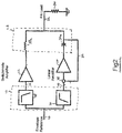
- Figure 1 shows a prior art envelope tracking (ET) modulator architecture in which a frequency splitter 12 is used to divide an incoming envelope reference signal on line 10 into a high frequency (HF) path signal on line 14 and a low frequency (LF) path signal on line 16.
- the frequency splitter 12 may include a low pass filter 18 in the low frequency path and a high pass filter 20 in the high frequency path.
- the signal in the LF path on line 16 is amplified by an efficient switched mode amplifier 22, and the signal in the HF path on line 14 is amplified by a wideband linear amplifier 24.
- a frequency selective combiner 26 is used to combine the signals in the LF and HF paths after amplification.
- the combiner 26 is illustrated as including a low frequency combining element (and high frequency blocking element) 28 in the low frequency path, and a high frequency combining element (and low frequency blocking element) 30 in the high frequency path.
- a combined signal from the combiner 26 on line 32 provides a feed to a load 34 which for the purposes of example is illustrated as a resistor.
- the load is a power amplifier (PA), and the reference signal is derived from an input signal to be amplified by the power amplifier.
- PA power amplifier
- FIG 2 shows an alternative prior art arrangement in which the frequency selective combiner 26 is an inductor-capacitor (LC) combiner.
- the low frequency combining element is an inductor 28a
- the high frequency combining element is a capacitor 30a.
- a feedback path 36 takes a signal from the combiner (or modulator) output on line 32, to the input of the linear amplifier 24.
- the signal on the feedback path 36 is subtracted from the signal in the high frequency path on line 14 by subtractor 38, to provide an input to the linear amplifier 24.
- the inclusion of the feedback path 36 achieves improved tracking accuracy compared to the arrangement of Figure 1 .
- the invention provides an envelope tracking power supply arranged to generate a modulated supply voltage in dependence on a reference signal, comprising a first path for tracking low frequency variations in the reference signal and a second path for tracking high frequency variations in the reference signal, the second path including a linear amplifier, wherein the output stage of the linear amplifier comprises a current source and a current sink connected to the high frequency output, there further being provided a DC offset current at the high frequency output.
- the DC offset current may be chosen to minimise the power dissipated in the output stage of the linear amplifier.
- the DC offset current may be derived from a further voltage supply which is lower than the output stage voltage supply.
- the DC offset current may be provided via an inductor connected between the further power supply and the high frequency output
- the envelope tracking power supply senses the difference between the power dissipated in the current source and the current sink, and integrates the sensed power difference to control a switch mode converter to generate a second supply voltage to generate the DC offset current.
- Sensing the power difference may comprise measuring a supply voltage for generating the DC offset current, the output voltage, the source current and the sink current.
- a target DC offset current may be determined in dependence on the difference between the input voltage waveform and the halved sum of the maximum and minimum voltage levels of the input waveform voltage.
- An error between the target DC offset current and a measured DC offset current may integrated and used to control a switch mode converter to generate a second supply voltage to generate the DC offset current.
- An RF amplifier may include an envelope tracking power supply.
- a mobile device for a mobile communication system may include an envelope tracking power supply.
- An infrastructure element for a mobile communications system may include an envelope tracking power supply.
- the invention further provides a method for an envelope tracking power supply arranged to generate a modulated supply voltage in dependence on a reference signal, comprising providing a first path for tracking low frequency variations in the reference signal and providing a second path for tracking high frequency variations in the reference signal, the second path including a linear amplifier, wherein the output stage of the linear amplifier comprises a current source and a current sink connected to the high frequency output, the method further comprising providing a DC offset current at the high frequency output.
- Embodiments of the invention may apply to different feedback architectures for the linear amplifier in the high frequency path.
- the invention and its embodiments are not limited to a particular feedback arrangement in the high frequency path.
- an arrangement is illustrated in which the linear amplifier receives a feedback from the output of the combiner.
- the present invention may also apply, for example, to an arrangement in which the linear amplifier receives a feedback from the output of the linear amplifier at the input to the combiner, and in which the path containing the linear amplifier does not include a high frequency filter such as filter 20 in Figure 2 , the linear amplifier path receiving the full-spectrum reference signal.
- FIG. 3 illustrates an exemplary implementation of the linear amplifier 24 Class B output stage.
- a current source 250 is connected between a supply voltage V SUPPLY and a common node 254, and a current sink 252 is connected between the common node 254 and electrical ground V GND .
- An instantaneous source current I SRC flows in the current source element 250, and an instantaneous current I SNK flows in the current sink element 252. At any given instant current flows in either the source device 250 or the sink device 252, and the current in the inactive device is zero.
- An output voltage V EA is formed at node 254.
- the combiner capacitor 30a of Figure 2 is illustrated as connected between the node 254 and the output of the combiner. A current I EA flows in the combiner capacitor 30a.
- the arrangement of Figure 3 shows a feedback path 40 which represents a feedback from the output of the linear amplifier, before the combiner, to the input of the linear amplifier.
- the feedback is not described in more detail herein because it does not form part of the present invention.
- the current flow in the feedback path is assumed to be sufficiently low to be ignored.
- the required modulator output voltage provided by the linear amplifier 24 may typically exhibit significant asymmetry, and this in turn results in asymmetry of the output current I EA of the linear amplifier 24.
- the line 304 in Figure 4(b) shows the average current in source device 250 and the line 306 in Figure 4(c) shows the average current in the sink device 252.
- the average current in source device 250 is equal to the average current in sink device 252.
- the power dissipated in the upper device is much greater than the power dissipated in the lower device (current sink 252).
- This disparity in power dissipation is due to the waveform asymmetry and results in much higher voltages across the upper (source) device.
- an extra voltage supply is used to add a DC (or low frequency) offset current via an inductor to the output node of the linear amplifier 24.
- Figure 5 shows such a modified topology.
- the arrangement of Figure 3 is modified such that an inductor 256 is included between a second supply voltage V SUPPLY2 and the node 254.
- the inductor 256 provides an offset current I OS, which flows in the inductor 256 from the voltage supply V SUPPLY2 .
- the instantaneous current in the current source 250 is modified to I SRC' and the instantaneous current in the current sink 252 is I SNK' .
- the output current I EA flows in the output capacitor 30a, and the output voltage V EA is formed at the node 254.
- the waveform of Figure 6(a) shows the output current I EA of the linear amplifier 24, which is the same as that shown in Figure 4(a) .
- the output current I EA of the linear amplifier is unchanged.
- the portion of the output current above the line 602 is provided by the source transistor 250.
- the portion of the output current below the line 602 is provided by the sink transistor 252.
- Figures 6(b) and 6(c) show the modified source I SRC' and sink I SNK' currents from the current source element 250 and current sink element 252 respectively.
- the modified source current I SRC' is decreased by offset current Ios and the modified sink current is increased by offset current Ios.
- the lines 604 and 606 in the respective Figures 6(b) and 6(c) represent the modified average currents flowing in the respective source and sink transistors.
- the effect of the additional offset current I OS supplied via inductor 256 is to reduce the average source current by I os from I SRC to I SRC' , and increase the average sink current by I os from I SNK to I SNK' . This reduces the power dissipated in the current source 250 and increases the power dissipated in the current sink 252.
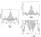
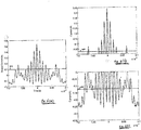
- Figure 7(a) shows the dissipation 702, 704 in the output stage source and sink current devices 250 and 252 respectively, and the total dissipation 706, as a function of the offset current I OS for the arrangement of Figure 5 .
- the instantaneous power dissipation in the source and sink output devices 250 and 252 cannot easily be directly measured, but the average current through the source and sink devices 250 and 252 and the average output voltage can all be readily measured. Hence it is possible to calculate the 'sensed' powers as a proxy for the dissipated powers using these average parameters.
- Figure 7(b) shows the sensed powers for the source device 710, sink device 708 and the total sensed power 712.
- Inductor 250 ideally has zero DC resistance, hence the DC voltage at both terminals of the inductor 250 is the same.
- the sensed source power can be calculated as: avg V SUPPLY ⁇ V EA ⁇ avg I SRC ′
- the sensed sink power can be calculated as: avg V EA ⁇ avg I SNK ′ where:
- the minimum in total sensed power occurs at the same value of offset current as the minimum dissipated power, as shown in Figure 7 , hence minimising sensed power maximises the efficiency of the supply modulator.
- the additional voltage supply V SUPPLY2 in Figure 5 is assumed to be generated using a high efficiency power converter, and the power loss in feed inductor 256 is assumed to be minimal.
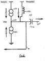
- Figure 8 shows a direct technique for generating the offset current in which a negative feedback loop may be used to minimise the total sensed power by minimising the difference between the two sensed powers, by integrating the error to make small adjustments to the output voltage of the second supply V SUPPLY2 .
- Figure 8 shows the output stage of the error amplifier comprising current source 250, current sink 252, combining capacitor 30a and DC current offset feed inductor 256.
- the supply voltage V SUPPLY2 is provided by a switch mode converter 810, which is connected to a supply voltage V SUPPLY denoted by reference numeral 814.
- the input to the switch mode converter 810 is provided by an integrator 816.
- the input to the integrator 816 is provided by a signal processing block 820, which generates a signal representing the sensed power difference on line 818 to the input of the integrator 816 based on the second supply voltage Vsupply2, the average output voltage Vea, and the average of the source and sink currents I SRC' and I SNK' .
- An indirect method of controlling the offset current exploits the fact that the offset current required depends on the asymmetry of the waveform. If the waveform is symmetrical the mean voltage lies midway between the minimum and maximum values of the waveform. If the mean voltage is less than midway between the minimum and maximum values of the waveform a positive offset current is required to minimise the output stage power dissipation. Similarly if the mean voltage is greater than midway between the minimum and maximum values of the waveform a negative offset current is required to minimise the output stage dissipation.
- Figure 9 shows a control loop for implementing this indirect concept.
- the control loop includes the current source 250 and current sink 252 of the output stage, the combining capacitor 30a, and the DC current offset feed inductor 256.
- the inductor 256 is connected to the node 254 via current sense resistor 800.
- the supply voltage Vsupply2 is provided by a switch mode converter 802, which is connected to a supply voltage V SUPPLY denoted by reference numeral 804.
- the input to the switch mode converter is provided by an integrator 806.
- a first input of the integrator is provided by a subtractor 808, which provides a difference on line 812 between the voltage which is midway between the minimum and maximum values of the input waveform (equal to (Vmax+Vmin)/2) and the input waveform Vin 810 to give a voltage representative of the offset current target on line 814 at the first input to the integrator 806.
- the second input to the integrator 806 is provided by a voltage source 816, which measures the current in the resistor 800 and provides a voltage representing the offset current.
- the current offset target on line 814 is set as the difference between the mean and median waveform voltages as described above.
- the error between the target and measured offset current is integrated by integrator 806 and used to control the switch mode converter 802 which generates the second supply voltage V SUPPLY2 which supplies the offset current to the linear amplifier output stage via the inductor 256.
- the generation of the offset current and the second supply may be achieved in a number of ways, both indirectly and directly, and the invention is not limited to any particular technique.
- the present invention may be applied to the output of a linear amplifier in a correction path of a modulated power supply, such as the linear amplifier of Figure 1 or Figure 2 .
- Such modulated power supplies may be used to provide the modulated power supply to an RF amplifier, which may comprises the load of Figure 1 or Figure 2 .
- RF amplifiers are used in mobile communication systems, in wireless devices and wireless infrastructure.
- the invention and its embodiments relates to the application of envelope tracking (ET) to radio frequency (RF) power amplifiers, and is applicable to a broad range of implementations including cellular handsets, wireless infrastructure, and military power amplifier applications at high frequencies to microwave frequencies.
- ET envelope tracking
- RF radio frequency
Description
- The invention relates to envelope tracking modulated power supplies suitable for radio frequency power amplifier applications. The invention is particularly concerned with such power supplies in which a reference signal is used as an input to a low frequency path and a high frequency path, and in which each path generates separate outputs which are combined to form a supply voltage.
- Envelope tracking power supplies for radio frequency power amplifiers are well-known in the art. Typically a reference signal is generated based on an envelope of an input signal to be amplified. An envelope tracking power supply generates a supply voltage for the power amplifier which tracks the reference signal.
-
Figure 1 shows a prior art envelope tracking (ET) modulator architecture in which afrequency splitter 12 is used to divide an incoming envelope reference signal online 10 into a high frequency (HF) path signal online 14 and a low frequency (LF) path signal on line 16. Thefrequency splitter 12 may include a low pass filter 18 in the low frequency path and a high pass filter 20 in the high frequency path. The signal in the LF path on line 16 is amplified by an efficient switched mode amplifier 22, and the signal in the HF path online 14 is amplified by a wideband linear amplifier 24. A frequencyselective combiner 26 is used to combine the signals in the LF and HF paths after amplification. InFigure 1 thecombiner 26 is illustrated as including a low frequency combining element (and high frequency blocking element) 28 in the low frequency path, and a high frequency combining element (and low frequency blocking element) 30 in the high frequency path. A combined signal from thecombiner 26 online 32 provides a feed to aload 34 which for the purposes of example is illustrated as a resistor. In a typical application the load is a power amplifier (PA), and the reference signal is derived from an input signal to be amplified by the power amplifier. - An example of a power amplifier system incorporating a supply architecture such as illustrated in
Figure 1 can be found in "Band Separation and Efficiency Optimisation in Linear-Assisted Switching Power Amplifiers", Yousefzadeh et al, [IEEE Power Electronics Specialists Conference 2006]. -
Figure 2 shows an alternative prior art arrangement in which the frequencyselective combiner 26 is an inductor-capacitor (LC) combiner. The low frequency combining element is an inductor 28a, and the high frequency combining element is acapacitor 30a. In this arrangement afeedback path 36 takes a signal from the combiner (or modulator) output online 32, to the input of the linear amplifier 24. The signal on thefeedback path 36 is subtracted from the signal in the high frequency path online 14 bysubtractor 38, to provide an input to the linear amplifier 24. The inclusion of thefeedback path 36 achieves improved tracking accuracy compared to the arrangement ofFigure 1 . - An example of a power amplifier system incorporating a supply architecture such as illustrated in
Figure 2 can be found in "Efficiency Optimisation in Linear-Assisted Switching Power Converters for Envelope Tracking in RF Power Amplifiers", Yousefzadeh et al, [IEEE Symposium on Circuits and Systems 2005]. - It is an aim of the invention to provide an envelope tracking modulated power supply which offers improvements over the prior art, such as the arrangements of
Figures 1 and2 . Additional hybrid envelope tracking power supplies are known from Chin et al: 'Digitally Assisted Dual-Switch High-Efficiency Envelope Amplifier for Envelope-Tracking Base-Station Power Amplifiers', IEEE Transactions on Microwave Theory and Techniques, 2011-11-01, vol. 59, No. 11, pages 2943-2953; and Staut et al: 'Optimum Bias Calculation for Parallel Hybrid Switching-Linear Regulators', Applied Power Electronics Conference, APEC 2007 - Twenty Second Annual IEEE, pages 569-573. - The invention provides an envelope tracking power supply arranged to generate a modulated supply voltage in dependence on a reference signal, comprising a first path for tracking low frequency variations in the reference signal and a second path for tracking high frequency variations in the reference signal, the second path including a linear amplifier, wherein the output stage of the linear amplifier comprises a current source and a current sink connected to the high frequency output, there further being provided a DC offset current at the high frequency output.
- The DC offset current may be chosen to minimise the power dissipated in the output stage of the linear amplifier.
- The DC offset current may be derived from a further voltage supply which is lower than the output stage voltage supply.
- The DC offset current may be provided via an inductor connected between the further power supply and the high frequency output
- The envelope tracking power supply, in a first embodiment, senses the difference between the power dissipated in the current source and the current sink, and integrates the sensed power difference to control a switch mode converter to generate a second supply voltage to generate the DC offset current. Sensing the power difference may comprise measuring a supply voltage for generating the DC offset current, the output voltage, the source current and the sink current.
- Alternatively, a target DC offset current may be determined in dependence on the difference between the input voltage waveform and the halved sum of the maximum and minimum voltage levels of the input waveform voltage. An error between the target DC offset current and a measured DC offset current may integrated and used to control a switch mode converter to generate a second supply voltage to generate the DC offset current.
- An RF amplifier may include an envelope tracking power supply.
- A mobile device for a mobile communication system may include an envelope tracking power supply.
- An infrastructure element for a mobile communications system may include an envelope tracking power supply.
- The invention further provides a method for an envelope tracking power supply arranged to generate a modulated supply voltage in dependence on a reference signal, comprising providing a first path for tracking low frequency variations in the reference signal and providing a second path for tracking high frequency variations in the reference signal, the second path including a linear amplifier, wherein the output stage of the linear amplifier comprises a current source and a current sink connected to the high frequency output, the method further comprising providing a DC offset current at the high frequency output.
- The invention is now described by way of example with reference to the accompanying Figures, in which:
-
Figure 1 illustrates a prior art envelope tracking modulated supply with high and low frequency paths; -
Figure 2 illustrates a prior art envelope tracking modulated supply incorporating feedback in the high frequency path; -
Figure 3 illustrates a modified implementation an output of a linear amplifier in accordance with the arrangement ofFigure 1 orFigure 2 ; -
Figure 4(a) to 4(c) illustrate current flow in the arrangement ofFigure 3 ; -
Figure 5 illustrates the implementation of the output of a linear amplifier in the arrangement ofFigure 1 orFigure 2 in accordance with an embodiment of the present invention; -
Figures 6(a) to 6(c) illustrate current flow in the the arrangement ofFigure 5 ; -
Figures 7(a) and 7(d) illustrate waveform plots in the arrangement ofFigures 3 and5 ; -
Figure 8 illustrates the implementation of the output of a linear amplifier in the arrangement ofFigure 1 orFigure 2 in accordance with an exemplary embodiment of the present invention; and -
Figure 9 illustrates the implementation of the output of a linear amplifier in the arrangement ofFigure 1 orFigure 2 in accordance with another exemplary embodiment of the present invention. - In the following description the invention is described with reference to exemplary embodiments and implementations. The invention is not limited to the specific details of any arrangements as set out, which are provided for the purposes of understanding the invention.
- Embodiments of the invention may apply to different feedback architectures for the linear amplifier in the high frequency path. The invention and its embodiments are not limited to a particular feedback arrangement in the high frequency path. For example in the foregoing illustration of
Figure 2 an arrangement is illustrated in which the linear amplifier receives a feedback from the output of the combiner. The present invention may also apply, for example, to an arrangement in which the linear amplifier receives a feedback from the output of the linear amplifier at the input to the combiner, and in which the path containing the linear amplifier does not include a high frequency filter such as filter 20 inFigure 2 , the linear amplifier path receiving the full-spectrum reference signal. - In general in a hybrid envelope tracking modulator (i.e. an architecture using a switched mode amplifier and a linear amplifier) as illustrated in
Figure 2 , a significant proportion of the total modulator power dissipation occurs in the output stage of the linear amplifier. - This can be understood with reference to
Figure 3 , which illustrates an exemplary implementation of the linear amplifier 24 Class B output stage. As illustrated, acurrent source 250 is connected between a supply voltage VSUPPLY and acommon node 254, and acurrent sink 252 is connected between thecommon node 254 and electrical ground VGND. An instantaneous source current ISRC flows in thecurrent source element 250, and an instantaneous current ISNK flows in thecurrent sink element 252. At any given instant current flows in either thesource device 250 or thesink device 252, and the current in the inactive device is zero. An output voltage VEA is formed atnode 254. Thecombiner capacitor 30a ofFigure 2 is illustrated as connected between thenode 254 and the output of the combiner. A current IEA flows in thecombiner capacitor 30a. - For the purposes of example, the arrangement of
Figure 3 shows a feedback path 40 which represents a feedback from the output of the linear amplifier, before the combiner, to the input of the linear amplifier. The feedback is not described in more detail herein because it does not form part of the present invention. The current flow in the feedback path is assumed to be sufficiently low to be ignored. - No DC current can flow through the
combiner capacitor 30a. Hence in the prior art arrangement ofFigure 3 the value of the average source current ISRC fromcurrent source 250 must be equal to the value of the average sink current ISNK fromcurrent sink 252. - In general the required modulator output voltage provided by the linear amplifier 24 may typically exhibit significant asymmetry, and this in turn results in asymmetry of the output current IEA of the linear amplifier 24.
- This is illustrated by the waveform of
Figure 4(a) which shows a plot of output current IEA against time. The current above the zero level 302 represents output positive currents which flow in thesource transistor 250, and the current below the zero level 302 represents the output negative currents which flow in thesink transistor 252. The combined source and sink currents represent the output current IEA. - The values of each of the average source ISRC and sink ISNK currents are equal as shown in
Figures 4(b) and 4(c) , which shows plots of the source and sink currents against time. - The
line 304 inFigure 4(b) shows the average current insource device 250 and the line 306 inFigure 4(c) shows the average current in thesink device 252. The average current insource device 250 is equal to the average current insink device 252. - However in the example as shown the power dissipated in the upper device (the current source 250) is much greater than the power dissipated in the lower device (current sink 252). This disparity in power dissipation is due to the waveform asymmetry and results in much higher voltages across the upper (source) device.
- It can thus be seen that the necessity for the average sink and source currents to be equal for the output topology of
Figure 3 is disadvantageous. - In accordance with a preferred embodiment of the invention, an extra voltage supply is used to add a DC (or low frequency) offset current via an inductor to the output node of the linear amplifier 24. There is thus no longer a requirement for the average source and sink currents to be equal.
-
Figure 5 shows such a modified topology. The arrangement ofFigure 3 is modified such that aninductor 256 is included between a second supply voltage VSUPPLY2 and thenode 254. Theinductor 256 provides an offset current IOS, which flows in theinductor 256 from the voltage supply VSUPPLY2. - The instantaneous current in the
current source 250 is modified to ISRC' and the instantaneous current in thecurrent sink 252 is ISNK'. The output current IEA flows in theoutput capacitor 30a, and the output voltage VEA is formed at thenode 254. - The waveform of
Figure 6(a) shows the output current IEA of the linear amplifier 24, which is the same as that shown inFigure 4(a) . In accordance with the invention therefore, the output current IEA of the linear amplifier is unchanged. As illustrated inFigure 6 , the portion of the output current above the line 602 is provided by thesource transistor 250. The portion of the output current below the line 602 is provided by thesink transistor 252. -
Figures 6(b) and 6(c) show the modified source ISRC' and sink ISNK' currents from thecurrent source element 250 andcurrent sink element 252 respectively. In the example shown the modified source current ISRC' is decreased by offset current Ios and the modified sink current is increased by offset current Ios. The lines 604 and 606 in the respectiveFigures 6(b) and 6(c) represent the modified average currents flowing in the respective source and sink transistors. - As illustrated, by comparing
Figures 4(b) and 4(c) withFigures 6(b) and 6(c) , the effect of the additional offset current IOS supplied viainductor 256 is to reduce the average source current by Ios from ISRC to ISRC', and increase the average sink current by Ios from ISNK to ISNK'. This reduces the power dissipated in thecurrent source 250 and increases the power dissipated in thecurrent sink 252. -
Figure 7(a) shows thedissipation 702, 704 in the output stage source and sinkcurrent devices total dissipation 706, as a function of the offset current IOS for the arrangement ofFigure 5 . - It can be seen that for the particular waveform illustrated the minimum dissipation in
Figure 7(a) is approximately 20% less than the dissipation with no offset current. This difference in dissipation is strongly dependant on the waveform asymmetry and is larger for more asymmetric waveforms. - The instantaneous power dissipation in the source and sink
output devices devices -
Figure 7(b) shows the sensed powers for the source device 710, sink device 708 and the total sensed power 712. -
Inductor 250 ideally has zero DC resistance, hence the DC voltage at both terminals of theinductor 250 is the same. - Referring to
Figure 5 , the sensed source power can be calculated as:
- The sensed sink power can be calculated as:

- VSUPPLY
- = the supply voltage applied to the feed inductor;
- VEA
- = the output voltage of the stage;
- avg (ISRC')
- = the average source current; and
- avg (ISNK')
- = the average sink current.
- The minimum in total sensed power occurs at the same value of offset current as the minimum dissipated power, as shown in
Figure 7 , hence minimising sensed power maximises the efficiency of the supply modulator. - The additional voltage supply VSUPPLY2 in
Figure 5 is assumed to be generated using a high efficiency power converter, and the power loss infeed inductor 256 is assumed to be minimal. -
Figure 8 shows a direct technique for generating the offset current in which a negative feedback loop may be used to minimise the total sensed power by minimising the difference between the two sensed powers, by integrating the error to make small adjustments to the output voltage of the second supply VSUPPLY2 . -
Figure 8 shows the output stage of the error amplifier comprisingcurrent source 250,current sink 252, combiningcapacitor 30a and DC current offsetfeed inductor 256. The supply voltage VSUPPLY2 is provided by a switch mode converter 810, which is connected to a supply voltage VSUPPLY denoted by reference numeral 814. - The input to the switch mode converter 810 is provided by an integrator 816. The input to the integrator 816 is provided by a signal processing block 820, which generates a signal representing the sensed power difference on line 818 to the input of the integrator 816 based on the second supply voltage Vsupply2, the average output voltage Vea, and the average of the source and sink currents ISRC' and ISNK'.
- An indirect method of controlling the offset current exploits the fact that the offset current required depends on the asymmetry of the waveform. If the waveform is symmetrical the mean voltage lies midway between the minimum and maximum values of the waveform. If the mean voltage is less than midway between the minimum and maximum values of the waveform a positive offset current is required to minimise the output stage power dissipation. Similarly if the mean voltage is greater than midway between the minimum and maximum values of the waveform a negative offset current is required to minimise the output stage dissipation.
-
Figure 9 shows a control loop for implementing this indirect concept. - The control loop includes the
current source 250 andcurrent sink 252 of the output stage, the combiningcapacitor 30a, and the DC current offsetfeed inductor 256. Theinductor 256 is connected to thenode 254 viacurrent sense resistor 800. - The supply voltage Vsupply2 is provided by a switch mode converter 802, which is connected to a supply voltage VSUPPLY denoted by reference numeral 804.
- The input to the switch mode converter is provided by an
integrator 806. A first input of the integrator is provided by asubtractor 808, which provides a difference on line 812 between the voltage which is midway between the minimum and maximum values of the input waveform (equal to (Vmax+Vmin)/2) and the input waveform Vin 810 to give a voltage representative of the offset current target on line 814 at the first input to theintegrator 806. The second input to theintegrator 806 is provided by a voltage source 816, which measures the current in theresistor 800 and provides a voltage representing the offset current. - The current offset target on line 814 is set as the difference between the mean and median waveform voltages as described above. The error between the target and measured offset current is integrated by
integrator 806 and used to control the switch mode converter 802 which generates the second supply voltage VSUPPLY2 which supplies the offset current to the linear amplifier output stage via theinductor 256. - The generation of the offset current and the second supply may be achieved in a number of ways, both indirectly and directly, and the invention is not limited to any particular technique.
- As discussed above the present invention may be applied to the output of a linear amplifier in a correction path of a modulated power supply, such as the linear amplifier of
Figure 1 orFigure 2 . - Such modulated power supplies may be used to provide the modulated power supply to an RF amplifier, which may comprises the load of
Figure 1 orFigure 2 . - RF amplifiers are used in mobile communication systems, in wireless devices and wireless infrastructure.
- The invention and its embodiments relates to the application of envelope tracking (ET) to radio frequency (RF) power amplifiers, and is applicable to a broad range of implementations including cellular handsets, wireless infrastructure, and military power amplifier applications at high frequencies to microwave frequencies.
- The invention has been described herein by way of example with reference to embodiments. The invention is not limited to the described embodiments, nor to specific combinations of features in embodiments. Modifications may be made to the embodiments within the scope of the invention. The scope of the invention is defined by the appended claims.
Claims (11)
- An envelope tracking power supply arranged to generate a modulated supply voltage in dependence on a reference signal, comprising a first path for tracking low frequency variations in the reference signal and a second path for tracking high frequency variations in the reference signal, the second path including a linear amplifier, wherein the output stage of the linear amplifier comprises a current source (250) and a current sink (252) connected to the high frequency output, there further being provided a DC offset current at the high frequency output, and sensing (820) the power difference between the power dissipated in the current source and the current sink, and integrating (816) the sensed power difference to control a switch mode converter (810) to generate a second supply voltage to generate the DC offset current.
- The envelope tracking power supply of claim 1 wherein the DC offset current is chosen to minimise the power dissipated in the output stage of the linear amplifier, or wherein the DC offset current is derived from a further voltage supply which is lower than the output stage voltage supply, or wherein the DC offset current is provided via an inductor connected between the further power supply and the high frequency output.
- The envelope tracking power supply of claim 1 wherein sensing the power difference comprises measuring a supply voltage for generating the DC offset current, the output voltage, the source current and the sink current.
- An envelope tracking power supply arranged to generate a modulated supply voltage in dependence on a reference signal, comprising a first path for tracking low frequency variations in the reference signal and a second path for tracking high frequency variations in the reference signal, the second path including a linear amplifier, wherein the output stage of the linear amplifier comprises a current source (250) and a current sink (252) connected to the high frequency output, there further being provided a DC offset current at the high frequency output, wherein a target DC offset current is determined (808) in dependence on the difference between the input voltage waveform and the halved sum of the maximum and minimum voltage levels of the input waveform voltage.
- The envelope tracking power supply of claim 4 wherein an error between the target DC offset current and a measured DC offset current is integrated and used to control a switch mode converter to generate a second supply voltage to generate the DC offset current.
- An RF amplifier or a mobile device for a mobile communication system or an infrastructure element for a mobile communication system including an envelope tracking power supply according to any one of claims 1 to 5.
- A method for an envelope tracking power supply arranged to generate a modulated supply voltage in dependence on a reference signal, comprising providing a first path for tracking low frequency variations in the reference signal and providing a second path for tracking high frequency variations in the reference signal, the second path including a linear amplifier, wherein the output stage of the linear amplifier comprises a current source and a current sink connected to the high frequency output, the method further comprising providing a DC offset current at the high frequency output, and sensing the power differencebetween the power dissipated in the current source and the current sink, and integrating the sensed power difference to control a switch mode converter to generate a second supply voltage to generate the DC offset current.
- The method of claim 7 wherein the DC offset current is chosen to minimise the power dissipated in the output stage of the linear amplifier, or wherein the DC offset current is derived from a further voltage supply which is lower than the output stage voltage supply, or wherein the DC offset current is provided via an inductor connected between the further power supply and the high frequency output.
- The method of claim 7 wherein sensing the power difference comprises measuring a supply voltage for generating the DC offset current, the output voltage, the source current and the sink current.
- A method for an envelope tracking power supply arranged to generate a modulated supply voltage in dependence on a reference signal, comprising providing a first path for tracking low frequency variations in the reference signal and providing a second path for tracking high frequency variations in the reference signal, the second path including a linear amplifier, wherein the output stage of the linear amplifier comprises a current source and a current sink connected to the high frequency output, the method further comprising providing a DC offset current at the high frequency output, wherein a target DC offset current is determined in dependence on the difference between the input voltage waveform and the halved sum of the maximum and minimum voltage levels of the input waveform voltage.
- The method of claim 10 wherein an error between the target DC offset current and a measured DC offset current is integrated and used to control a switch mode converter to generate a second supply voltage to generate the DC offset current.
Priority Applications (1)
| Application Number | Priority Date | Filing Date | Title |
|---|---|---|---|
| EP19201054.4A EP3667905B1 (en) | 2013-02-01 | 2014-01-31 | Improved efficiency for linear amplifier of envelope tracking modulator |
Applications Claiming Priority (2)
| Application Number | Priority Date | Filing Date | Title |
|---|---|---|---|
| GB1301852.8A GB2510393A (en) | 2013-02-01 | 2013-02-01 | An envelope-tracking amplifier with a linear amplifier having an output offset current for improved efficiency |
| PCT/EP2014/051967 WO2014118347A1 (en) | 2013-02-01 | 2014-01-31 | Improved efficiency for linear amplifier of envelope tracking modulator |
Related Child Applications (2)
| Application Number | Title | Priority Date | Filing Date |
|---|---|---|---|
| EP19201054.4A Division-Into EP3667905B1 (en) | 2013-02-01 | 2014-01-31 | Improved efficiency for linear amplifier of envelope tracking modulator |
| EP19201054.4A Division EP3667905B1 (en) | 2013-02-01 | 2014-01-31 | Improved efficiency for linear amplifier of envelope tracking modulator |
Publications (2)
| Publication Number | Publication Date |
|---|---|
| EP2951920A1 EP2951920A1 (en) | 2015-12-09 |
| EP2951920B1 true EP2951920B1 (en) | 2019-12-11 |
Family
ID=47988592
Family Applications (2)
| Application Number | Title | Priority Date | Filing Date |
|---|---|---|---|
| EP19201054.4A Active EP3667905B1 (en) | 2013-02-01 | 2014-01-31 | Improved efficiency for linear amplifier of envelope tracking modulator |
| EP14702042.4A Active EP2951920B1 (en) | 2013-02-01 | 2014-01-31 | Improved efficiency for linear amplifier of envelope tracking modulator |
Family Applications Before (1)
| Application Number | Title | Priority Date | Filing Date |
|---|---|---|---|
| EP19201054.4A Active EP3667905B1 (en) | 2013-02-01 | 2014-01-31 | Improved efficiency for linear amplifier of envelope tracking modulator |
Country Status (7)
| Country | Link |
|---|---|
| US (1) | US9634612B2 (en) |
| EP (2) | EP3667905B1 (en) |
| JP (1) | JP6452623B2 (en) |
| KR (1) | KR20150117678A (en) |
| CN (2) | CN110708026B (en) |
| GB (1) | GB2510393A (en) |
| WO (1) | WO2014118347A1 (en) |
Families Citing this family (12)
| Publication number | Priority date | Publication date | Assignee | Title |
|---|---|---|---|---|
| US10063063B2 (en) | 2013-12-12 | 2018-08-28 | Ohio State Innovation Foundation | Harmonic harvester for improved RF-to-DC rectifying efficiency |
| US9530719B2 (en) | 2014-06-13 | 2016-12-27 | Skyworks Solutions, Inc. | Direct die solder of gallium arsenide integrated circuit dies and methods of manufacturing gallium arsenide wafers |
| US9445371B2 (en) | 2014-08-13 | 2016-09-13 | Skyworks Solutions, Inc. | Apparatus and methods for wideband envelope tracking systems |
| US10103693B2 (en) | 2015-09-30 | 2018-10-16 | Skyworks Solutions, Inc. | Power amplifier linearization system and method |
| US10110169B2 (en) | 2016-09-14 | 2018-10-23 | Skyworks Solutions, Inc. | Apparatus and methods for envelope tracking systems with automatic mode selection |
| CN108206703B (en) * | 2016-12-20 | 2020-05-08 | 中芯国际集成电路制造(上海)有限公司 | Radio frequency transmitting circuit, transmitter and user terminal |
| US10236831B2 (en) | 2017-05-12 | 2019-03-19 | Skyworks Solutions, Inc. | Envelope trackers providing compensation for power amplifier output load variation |
| US10615757B2 (en) | 2017-06-21 | 2020-04-07 | Skyworks Solutions, Inc. | Wide bandwidth envelope trackers |
| US10516368B2 (en) | 2017-06-21 | 2019-12-24 | Skyworks Solutions, Inc. | Fast envelope tracking systems for power amplifiers |
| KR102454811B1 (en) * | 2017-07-18 | 2022-10-13 | 삼성전기주식회사 | Envelope-tracking current bias circuit with improved offset cancellation |
| EP3759813A4 (en) | 2018-03-01 | 2021-10-13 | Telefonaktiebolaget Lm Ericsson (Publ) | Envelope tracking supply modulator for power amplifier |
| US11581854B2 (en) * | 2018-04-26 | 2023-02-14 | Mediatek Inc. | Envelope tracking supply modulator topology for wipe-bandwidth radio frequency transmitter |
Family Cites Families (18)
| Publication number | Priority date | Publication date | Assignee | Title |
|---|---|---|---|---|
| US6084468A (en) * | 1997-10-06 | 2000-07-04 | Motorola, Inc. | Method and apparatus for high efficiency wideband power amplification |
| US6590940B1 (en) * | 1999-05-17 | 2003-07-08 | Ericsson Inc. | Power modulation systems and methods that separately amplify low and high frequency portions of an amplitude waveform |
| NO321759B1 (en) | 2003-10-24 | 2006-07-03 | Nera Asa | Efficient power supply for fast varying power needs |
| GB2424137B (en) * | 2005-03-11 | 2007-02-14 | Audio Partnership Plc | Amplifier |
| GB2440772B (en) * | 2006-08-08 | 2011-11-30 | Asahi Chemical Micro Syst | Envelope modulator |
| WO2008105073A1 (en) * | 2007-02-27 | 2008-09-04 | Panasonic Corporation | Transmitter |
| GB0708733D0 (en) * | 2007-05-04 | 2007-06-13 | Nokia Corp | A device |
| US7783269B2 (en) | 2007-09-20 | 2010-08-24 | Quantance, Inc. | Power amplifier controller with polar transmitter |
| GB2457764B (en) * | 2008-02-28 | 2013-01-23 | Nujira Ltd | Improved control loop for amplification stage |
| US7808323B2 (en) * | 2008-05-23 | 2010-10-05 | Panasonic Corporation | High-efficiency envelope tracking systems and methods for radio frequency power amplifiers |
| JP2010213227A (en) * | 2009-03-12 | 2010-09-24 | Fujitsu Ltd | Power source circuit, and wireless communication circuit using same |
| JP2011009923A (en) * | 2009-06-24 | 2011-01-13 | Hitachi Kokusai Electric Inc | Power supply circuit of envelope tracking power supply, power amplifier, and radio base station |
| GB2488124B (en) * | 2011-02-15 | 2014-01-08 | Nujira Ltd | Control of cross-over point for a push-pull amplifier |
| JP5621649B2 (en) | 2011-02-18 | 2014-11-12 | 富士通株式会社 | Transmitter |
| CN102684494B (en) * | 2011-03-17 | 2014-10-29 | 中兴通讯股份有限公司 | Power supply modulation method and power supply modulator |
| US8698558B2 (en) * | 2011-06-23 | 2014-04-15 | Qualcomm Incorporated | Low-voltage power-efficient envelope tracker |
| JP6115477B2 (en) * | 2012-02-03 | 2017-04-19 | 日本電気株式会社 | Power supply device and transmission device using the same |
| US8854139B2 (en) * | 2012-05-30 | 2014-10-07 | Nujira Limited | Regulated cascode current mirror scheme for transconductance amplifiers |
-
2013
- 2013-02-01 GB GB1301852.8A patent/GB2510393A/en not_active Withdrawn
-
2014
- 2014-01-31 EP EP19201054.4A patent/EP3667905B1/en active Active
- 2014-01-31 KR KR1020157023234A patent/KR20150117678A/en not_active Application Discontinuation
- 2014-01-31 CN CN201911066474.5A patent/CN110708026B/en active Active
- 2014-01-31 WO PCT/EP2014/051967 patent/WO2014118347A1/en active Application Filing
- 2014-01-31 EP EP14702042.4A patent/EP2951920B1/en active Active
- 2014-01-31 CN CN201480018288.3A patent/CN105103441B/en active Active
- 2014-01-31 JP JP2015555733A patent/JP6452623B2/en not_active Expired - Fee Related
- 2014-01-31 US US14/764,806 patent/US9634612B2/en active Active
Non-Patent Citations (1)
| Title |
|---|
| None * |
Also Published As
| Publication number | Publication date |
|---|---|
| US9634612B2 (en) | 2017-04-25 |
| KR20150117678A (en) | 2015-10-20 |
| EP2951920A1 (en) | 2015-12-09 |
| GB2510393A (en) | 2014-08-06 |
| JP6452623B2 (en) | 2019-01-16 |
| CN110708026B (en) | 2023-08-18 |
| CN105103441B (en) | 2019-11-29 |
| GB201301852D0 (en) | 2013-03-20 |
| US20160006396A1 (en) | 2016-01-07 |
| EP3667905A1 (en) | 2020-06-17 |
| CN105103441A (en) | 2015-11-25 |
| WO2014118347A1 (en) | 2014-08-07 |
| JP2016505230A (en) | 2016-02-18 |
| CN110708026A (en) | 2020-01-17 |
| EP3667905B1 (en) | 2021-07-14 |
Similar Documents
| Publication | Publication Date | Title |
|---|---|---|
| EP2951920B1 (en) | Improved efficiency for linear amplifier of envelope tracking modulator | |
| US7949316B2 (en) | High-efficiency envelope tracking systems and methods for radio frequency power amplifiers | |
| JP6452622B2 (en) | Envelope tracking modulator with feedback | |
| KR102162783B1 (en) | Improved resonance suppression for envelope tracking modulator | |
| US20150358486A1 (en) | Improved voltage boost for et modulator | |
| US9270241B2 (en) | Power supply device, transmission device using same, and method for operating power supply device | |
| JP2016521102A (en) | Envelope tracker with variable boost power supply voltage | |
| US8198950B2 (en) | Power amplifier | |
| EP3223427A1 (en) | Btl output self-oscillating class d amplifier | |
| US9548700B2 (en) | Control of cross-over point | |
| Lazarević et al. | System linearity-based characterization of high-frequency multilevel dc–dc converters for S-band EER transmitters | |
| US9813025B2 (en) | Apparatus and method for power supply modulation | |
| US20190348957A1 (en) | Audio amplifier circuit | |
| Mahmoudidaryan | Hybrid Envelope Tracking Supply Modulator Analysis and Design for Wideband Applications | |
| GB2535180A (en) | AC amplifier output impedance reduction |
Legal Events
| Date | Code | Title | Description |
|---|---|---|---|
| PUAI | Public reference made under article 153(3) epc to a published international application that has entered the european phase |
Free format text: ORIGINAL CODE: 0009012 |
|
| 17P | Request for examination filed |
Effective date: 20150901 |
|
| AK | Designated contracting states |
Kind code of ref document: A1 Designated state(s): AL AT BE BG CH CY CZ DE DK EE ES FI FR GB GR HR HU IE IS IT LI LT LU LV MC MK MT NL NO PL PT RO RS SE SI SK SM TR |
|
| AX | Request for extension of the european patent |
Extension state: BA ME |
|
| DAX | Request for extension of the european patent (deleted) | ||
| STAA | Information on the status of an ep patent application or granted ep patent |
Free format text: STATUS: EXAMINATION IS IN PROGRESS |
|
| 17Q | First examination report despatched |
Effective date: 20190313 |
|
| RIC1 | Information provided on ipc code assigned before grant |
Ipc: H03F 3/19 20060101ALI20190515BHEP Ipc: H03F 1/02 20060101AFI20190515BHEP Ipc: H03F 3/217 20060101ALI20190515BHEP Ipc: H03F 3/21 20060101ALI20190515BHEP Ipc: H04W 52/02 20090101ALI20190515BHEP |
|
| GRAP | Despatch of communication of intention to grant a patent |
Free format text: ORIGINAL CODE: EPIDOSNIGR1 |
|
| STAA | Information on the status of an ep patent application or granted ep patent |
Free format text: STATUS: GRANT OF PATENT IS INTENDED |
|
| INTG | Intention to grant announced |
Effective date: 20190627 |
|
| GRAS | Grant fee paid |
Free format text: ORIGINAL CODE: EPIDOSNIGR3 |
|
| GRAA | (expected) grant |
Free format text: ORIGINAL CODE: 0009210 |
|
| STAA | Information on the status of an ep patent application or granted ep patent |
Free format text: STATUS: THE PATENT HAS BEEN GRANTED |
|
| AK | Designated contracting states |
Kind code of ref document: B1 Designated state(s): AL AT BE BG CH CY CZ DE DK EE ES FI FR GB GR HR HU IE IS IT LI LT LU LV MC MK MT NL NO PL PT RO RS SE SI SK SM TR |
|
| REG | Reference to a national code |
Ref country code: GB Ref legal event code: FG4D |
|
| REG | Reference to a national code |
Ref country code: CH Ref legal event code: EP |
|
| REG | Reference to a national code |
Ref country code: AT Ref legal event code: REF Ref document number: 1213193 Country of ref document: AT Kind code of ref document: T Effective date: 20191215 |
|
| REG | Reference to a national code |
Ref country code: DE Ref legal event code: R096 Ref document number: 602014058169 Country of ref document: DE |
|
| REG | Reference to a national code |
Ref country code: IE Ref legal event code: FG4D |
|
| REG | Reference to a national code |
Ref country code: NL Ref legal event code: MP Effective date: 20191211 |
|
| REG | Reference to a national code |
Ref country code: LT Ref legal event code: MG4D |
|
| PG25 | Lapsed in a contracting state [announced via postgrant information from national office to epo] |
Ref country code: NO Free format text: LAPSE BECAUSE OF FAILURE TO SUBMIT A TRANSLATION OF THE DESCRIPTION OR TO PAY THE FEE WITHIN THE PRESCRIBED TIME-LIMIT Effective date: 20200311 Ref country code: LT Free format text: LAPSE BECAUSE OF FAILURE TO SUBMIT A TRANSLATION OF THE DESCRIPTION OR TO PAY THE FEE WITHIN THE PRESCRIBED TIME-LIMIT Effective date: 20191211 Ref country code: GR Free format text: LAPSE BECAUSE OF FAILURE TO SUBMIT A TRANSLATION OF THE DESCRIPTION OR TO PAY THE FEE WITHIN THE PRESCRIBED TIME-LIMIT Effective date: 20200312 Ref country code: SE Free format text: LAPSE BECAUSE OF FAILURE TO SUBMIT A TRANSLATION OF THE DESCRIPTION OR TO PAY THE FEE WITHIN THE PRESCRIBED TIME-LIMIT Effective date: 20191211 Ref country code: LV Free format text: LAPSE BECAUSE OF FAILURE TO SUBMIT A TRANSLATION OF THE DESCRIPTION OR TO PAY THE FEE WITHIN THE PRESCRIBED TIME-LIMIT Effective date: 20191211 Ref country code: FI Free format text: LAPSE BECAUSE OF FAILURE TO SUBMIT A TRANSLATION OF THE DESCRIPTION OR TO PAY THE FEE WITHIN THE PRESCRIBED TIME-LIMIT Effective date: 20191211 Ref country code: BG Free format text: LAPSE BECAUSE OF FAILURE TO SUBMIT A TRANSLATION OF THE DESCRIPTION OR TO PAY THE FEE WITHIN THE PRESCRIBED TIME-LIMIT Effective date: 20200311 |
|
| PG25 | Lapsed in a contracting state [announced via postgrant information from national office to epo] |
Ref country code: RS Free format text: LAPSE BECAUSE OF FAILURE TO SUBMIT A TRANSLATION OF THE DESCRIPTION OR TO PAY THE FEE WITHIN THE PRESCRIBED TIME-LIMIT Effective date: 20191211 Ref country code: HR Free format text: LAPSE BECAUSE OF FAILURE TO SUBMIT A TRANSLATION OF THE DESCRIPTION OR TO PAY THE FEE WITHIN THE PRESCRIBED TIME-LIMIT Effective date: 20191211 |
|
| PG25 | Lapsed in a contracting state [announced via postgrant information from national office to epo] |
Ref country code: AL Free format text: LAPSE BECAUSE OF FAILURE TO SUBMIT A TRANSLATION OF THE DESCRIPTION OR TO PAY THE FEE WITHIN THE PRESCRIBED TIME-LIMIT Effective date: 20191211 |
|
| PG25 | Lapsed in a contracting state [announced via postgrant information from national office to epo] |
Ref country code: ES Free format text: LAPSE BECAUSE OF FAILURE TO SUBMIT A TRANSLATION OF THE DESCRIPTION OR TO PAY THE FEE WITHIN THE PRESCRIBED TIME-LIMIT Effective date: 20191211 Ref country code: PT Free format text: LAPSE BECAUSE OF FAILURE TO SUBMIT A TRANSLATION OF THE DESCRIPTION OR TO PAY THE FEE WITHIN THE PRESCRIBED TIME-LIMIT Effective date: 20200506 Ref country code: NL Free format text: LAPSE BECAUSE OF FAILURE TO SUBMIT A TRANSLATION OF THE DESCRIPTION OR TO PAY THE FEE WITHIN THE PRESCRIBED TIME-LIMIT Effective date: 20191211 Ref country code: RO Free format text: LAPSE BECAUSE OF FAILURE TO SUBMIT A TRANSLATION OF THE DESCRIPTION OR TO PAY THE FEE WITHIN THE PRESCRIBED TIME-LIMIT Effective date: 20191211 Ref country code: CZ Free format text: LAPSE BECAUSE OF FAILURE TO SUBMIT A TRANSLATION OF THE DESCRIPTION OR TO PAY THE FEE WITHIN THE PRESCRIBED TIME-LIMIT Effective date: 20191211 Ref country code: EE Free format text: LAPSE BECAUSE OF FAILURE TO SUBMIT A TRANSLATION OF THE DESCRIPTION OR TO PAY THE FEE WITHIN THE PRESCRIBED TIME-LIMIT Effective date: 20191211 |
|
| PG25 | Lapsed in a contracting state [announced via postgrant information from national office to epo] |
Ref country code: IS Free format text: LAPSE BECAUSE OF FAILURE TO SUBMIT A TRANSLATION OF THE DESCRIPTION OR TO PAY THE FEE WITHIN THE PRESCRIBED TIME-LIMIT Effective date: 20200411 Ref country code: SK Free format text: LAPSE BECAUSE OF FAILURE TO SUBMIT A TRANSLATION OF THE DESCRIPTION OR TO PAY THE FEE WITHIN THE PRESCRIBED TIME-LIMIT Effective date: 20191211 Ref country code: SM Free format text: LAPSE BECAUSE OF FAILURE TO SUBMIT A TRANSLATION OF THE DESCRIPTION OR TO PAY THE FEE WITHIN THE PRESCRIBED TIME-LIMIT Effective date: 20191211 |
|
| REG | Reference to a national code |
Ref country code: CH Ref legal event code: PL |
|
| REG | Reference to a national code |
Ref country code: DE Ref legal event code: R097 Ref document number: 602014058169 Country of ref document: DE |
|
| PG25 | Lapsed in a contracting state [announced via postgrant information from national office to epo] |
Ref country code: MC Free format text: LAPSE BECAUSE OF FAILURE TO SUBMIT A TRANSLATION OF THE DESCRIPTION OR TO PAY THE FEE WITHIN THE PRESCRIBED TIME-LIMIT Effective date: 20191211 |
|
| REG | Reference to a national code |
Ref country code: AT Ref legal event code: MK05 Ref document number: 1213193 Country of ref document: AT Kind code of ref document: T Effective date: 20191211 Ref country code: BE Ref legal event code: MM Effective date: 20200131 |
|
| PLBE | No opposition filed within time limit |
Free format text: ORIGINAL CODE: 0009261 |
|
| STAA | Information on the status of an ep patent application or granted ep patent |
Free format text: STATUS: NO OPPOSITION FILED WITHIN TIME LIMIT |
|
| PG25 | Lapsed in a contracting state [announced via postgrant information from national office to epo] |
Ref country code: LU Free format text: LAPSE BECAUSE OF NON-PAYMENT OF DUE FEES Effective date: 20200131 Ref country code: DK Free format text: LAPSE BECAUSE OF FAILURE TO SUBMIT A TRANSLATION OF THE DESCRIPTION OR TO PAY THE FEE WITHIN THE PRESCRIBED TIME-LIMIT Effective date: 20191211 |
|
| 26N | No opposition filed |
Effective date: 20200914 |
|
| PG25 | Lapsed in a contracting state [announced via postgrant information from national office to epo] |
Ref country code: AT Free format text: LAPSE BECAUSE OF FAILURE TO SUBMIT A TRANSLATION OF THE DESCRIPTION OR TO PAY THE FEE WITHIN THE PRESCRIBED TIME-LIMIT Effective date: 20191211 Ref country code: LI Free format text: LAPSE BECAUSE OF NON-PAYMENT OF DUE FEES Effective date: 20200131 Ref country code: PL Free format text: LAPSE BECAUSE OF FAILURE TO SUBMIT A TRANSLATION OF THE DESCRIPTION OR TO PAY THE FEE WITHIN THE PRESCRIBED TIME-LIMIT Effective date: 20191211 Ref country code: SI Free format text: LAPSE BECAUSE OF FAILURE TO SUBMIT A TRANSLATION OF THE DESCRIPTION OR TO PAY THE FEE WITHIN THE PRESCRIBED TIME-LIMIT Effective date: 20191211 Ref country code: BE Free format text: LAPSE BECAUSE OF NON-PAYMENT OF DUE FEES Effective date: 20200131 Ref country code: CH Free format text: LAPSE BECAUSE OF NON-PAYMENT OF DUE FEES Effective date: 20200131 |
|
| PG25 | Lapsed in a contracting state [announced via postgrant information from national office to epo] |
Ref country code: IE Free format text: LAPSE BECAUSE OF NON-PAYMENT OF DUE FEES Effective date: 20200131 Ref country code: IT Free format text: LAPSE BECAUSE OF FAILURE TO SUBMIT A TRANSLATION OF THE DESCRIPTION OR TO PAY THE FEE WITHIN THE PRESCRIBED TIME-LIMIT Effective date: 20191211 |
|
| PG25 | Lapsed in a contracting state [announced via postgrant information from national office to epo] |
Ref country code: TR Free format text: LAPSE BECAUSE OF FAILURE TO SUBMIT A TRANSLATION OF THE DESCRIPTION OR TO PAY THE FEE WITHIN THE PRESCRIBED TIME-LIMIT Effective date: 20191211 Ref country code: MT Free format text: LAPSE BECAUSE OF FAILURE TO SUBMIT A TRANSLATION OF THE DESCRIPTION OR TO PAY THE FEE WITHIN THE PRESCRIBED TIME-LIMIT Effective date: 20191211 Ref country code: CY Free format text: LAPSE BECAUSE OF FAILURE TO SUBMIT A TRANSLATION OF THE DESCRIPTION OR TO PAY THE FEE WITHIN THE PRESCRIBED TIME-LIMIT Effective date: 20191211 |
|
| PG25 | Lapsed in a contracting state [announced via postgrant information from national office to epo] |
Ref country code: MK Free format text: LAPSE BECAUSE OF FAILURE TO SUBMIT A TRANSLATION OF THE DESCRIPTION OR TO PAY THE FEE WITHIN THE PRESCRIBED TIME-LIMIT Effective date: 20191211 |
|
| PGFP | Annual fee paid to national office [announced via postgrant information from national office to epo] |
Ref country code: DE Payment date: 20221215 Year of fee payment: 10 |
|
| PGFP | Annual fee paid to national office [announced via postgrant information from national office to epo] |
Ref country code: GB Payment date: 20231218 Year of fee payment: 11 |
|
| PGFP | Annual fee paid to national office [announced via postgrant information from national office to epo] |
Ref country code: FR Payment date: 20231214 Year of fee payment: 11 |