EP2951636B1 - Capacitive sensor integrated in a display device - Google Patents
Capacitive sensor integrated in a display device Download PDFInfo
- Publication number
- EP2951636B1 EP2951636B1 EP14706953.8A EP14706953A EP2951636B1 EP 2951636 B1 EP2951636 B1 EP 2951636B1 EP 14706953 A EP14706953 A EP 14706953A EP 2951636 B1 EP2951636 B1 EP 2951636B1
- Authority
- EP
- European Patent Office
- Prior art keywords
- shield electrode
- sensor electrodes
- capacitive sensor
- polarizer
- conductive traces
- Prior art date
- Legal status (The legal status is an assumption and is not a legal conclusion. Google has not performed a legal analysis and makes no representation as to the accuracy of the status listed.)
- Active
Links
Images



Classifications
-
- G—PHYSICS
- G06—COMPUTING OR CALCULATING; COUNTING
- G06F—ELECTRIC DIGITAL DATA PROCESSING
- G06F3/00—Input arrangements for transferring data to be processed into a form capable of being handled by the computer; Output arrangements for transferring data from processing unit to output unit, e.g. interface arrangements
- G06F3/01—Input arrangements or combined input and output arrangements for interaction between user and computer
- G06F3/03—Arrangements for converting the position or the displacement of a member into a coded form
- G06F3/041—Digitisers, e.g. for touch screens or touch pads, characterised by the transducing means
- G06F3/0416—Control or interface arrangements specially adapted for digitisers
- G06F3/04164—Connections between sensors and controllers, e.g. routing lines between electrodes and connection pads
-
- G—PHYSICS
- G02—OPTICS
- G02F—OPTICAL DEVICES OR ARRANGEMENTS FOR THE CONTROL OF LIGHT BY MODIFICATION OF THE OPTICAL PROPERTIES OF THE MEDIA OF THE ELEMENTS INVOLVED THEREIN; NON-LINEAR OPTICS; FREQUENCY-CHANGING OF LIGHT; OPTICAL LOGIC ELEMENTS; OPTICAL ANALOGUE/DIGITAL CONVERTERS
- G02F1/00—Devices or arrangements for the control of the intensity, colour, phase, polarisation or direction of light arriving from an independent light source, e.g. switching, gating or modulating; Non-linear optics
- G02F1/01—Devices or arrangements for the control of the intensity, colour, phase, polarisation or direction of light arriving from an independent light source, e.g. switching, gating or modulating; Non-linear optics for the control of the intensity, phase, polarisation or colour
- G02F1/13—Devices or arrangements for the control of the intensity, colour, phase, polarisation or direction of light arriving from an independent light source, e.g. switching, gating or modulating; Non-linear optics for the control of the intensity, phase, polarisation or colour based on liquid crystals, e.g. single liquid crystal display cells
- G02F1/133—Constructional arrangements; Operation of liquid crystal cells; Circuit arrangements
- G02F1/1333—Constructional arrangements; Manufacturing methods
- G02F1/13338—Input devices, e.g. touch panels
-
- H—ELECTRICITY
- H03—ELECTRONIC CIRCUITRY
- H03K—PULSE TECHNIQUE
- H03K17/00—Electronic switching or gating, i.e. not by contact-making and –breaking
- H03K17/94—Electronic switching or gating, i.e. not by contact-making and –breaking characterised by the way in which the control signals are generated
- H03K17/96—Touch switches
- H03K17/962—Capacitive touch switches
- H03K17/9622—Capacitive touch switches using a plurality of detectors, e.g. keyboard
-
- G—PHYSICS
- G02—OPTICS
- G02F—OPTICAL DEVICES OR ARRANGEMENTS FOR THE CONTROL OF LIGHT BY MODIFICATION OF THE OPTICAL PROPERTIES OF THE MEDIA OF THE ELEMENTS INVOLVED THEREIN; NON-LINEAR OPTICS; FREQUENCY-CHANGING OF LIGHT; OPTICAL LOGIC ELEMENTS; OPTICAL ANALOGUE/DIGITAL CONVERTERS
- G02F1/00—Devices or arrangements for the control of the intensity, colour, phase, polarisation or direction of light arriving from an independent light source, e.g. switching, gating or modulating; Non-linear optics
- G02F1/01—Devices or arrangements for the control of the intensity, colour, phase, polarisation or direction of light arriving from an independent light source, e.g. switching, gating or modulating; Non-linear optics for the control of the intensity, phase, polarisation or colour
- G02F1/13—Devices or arrangements for the control of the intensity, colour, phase, polarisation or direction of light arriving from an independent light source, e.g. switching, gating or modulating; Non-linear optics for the control of the intensity, phase, polarisation or colour based on liquid crystals, e.g. single liquid crystal display cells
- G02F1/133—Constructional arrangements; Operation of liquid crystal cells; Circuit arrangements
- G02F1/1333—Constructional arrangements; Manufacturing methods
- G02F1/133308—Support structures for LCD panels, e.g. frames or bezels
- G02F1/133334—Electromagnetic shields
-
- G—PHYSICS
- G06—COMPUTING OR CALCULATING; COUNTING
- G06F—ELECTRIC DIGITAL DATA PROCESSING
- G06F2203/00—Indexing scheme relating to G06F3/00 - G06F3/048
- G06F2203/041—Indexing scheme relating to G06F3/041 - G06F3/045
- G06F2203/04107—Shielding in digitiser, i.e. guard or shielding arrangements, mostly for capacitive touchscreens, e.g. driven shields, driven grounds
-
- G—PHYSICS
- G06—COMPUTING OR CALCULATING; COUNTING
- G06F—ELECTRIC DIGITAL DATA PROCESSING
- G06F3/00—Input arrangements for transferring data to be processed into a form capable of being handled by the computer; Output arrangements for transferring data from processing unit to output unit, e.g. interface arrangements
- G06F3/01—Input arrangements or combined input and output arrangements for interaction between user and computer
- G06F3/03—Arrangements for converting the position or the displacement of a member into a coded form
- G06F3/041—Digitisers, e.g. for touch screens or touch pads, characterised by the transducing means
- G06F3/044—Digitisers, e.g. for touch screens or touch pads, characterised by the transducing means by capacitive means
-
- H—ELECTRICITY
- H03—ELECTRONIC CIRCUITRY
- H03K—PULSE TECHNIQUE
- H03K2217/00—Indexing scheme related to electronic switching or gating, i.e. not by contact-making or -breaking covered by H03K17/00
- H03K2217/94—Indexing scheme related to electronic switching or gating, i.e. not by contact-making or -breaking covered by H03K17/00 characterised by the way in which the control signal is generated
- H03K2217/96—Touch switches
- H03K2217/9607—Capacitive touch switches
- H03K2217/960755—Constructional details of capacitive touch and proximity switches
- H03K2217/960765—Details of shielding arrangements
-
- H—ELECTRICITY
- H03—ELECTRONIC CIRCUITRY
- H03K—PULSE TECHNIQUE
- H03K2217/00—Indexing scheme related to electronic switching or gating, i.e. not by contact-making or -breaking covered by H03K17/00
- H03K2217/94—Indexing scheme related to electronic switching or gating, i.e. not by contact-making or -breaking covered by H03K17/00 characterised by the way in which the control signal is generated
- H03K2217/96—Touch switches
- H03K2217/9607—Capacitive touch switches
- H03K2217/960785—Capacitive touch switches with illumination
- H03K2217/960795—Capacitive touch switches with illumination using organic light emitting devices, e.g. light emitting polymer [OEP] or OLED
Definitions
- Embodiments of the present invention relate to an apparatus.
- they relate to an apparatus comprising a plurality of capacitive sensor electrodes distributed over a sensing area.
- Current touch sensitive displays may use a plurality of capacitive sensor electrodes distributed over a sensing area.
- the capacitive sensor electrodes sense a proximal grounded object such as a user's finger touching the sensing area.
- US 2010/0220071 A1 discloses for example a capacitive touch panel arranged on a display and provided with shield electrodes overlying and underlying the detection electrodes.
- US2012/0081328 A1 discloses an electrode arrangement for a capacitive sensor device capable of detecting a position and/or an approach of an object.
- an apparatus comprising: a sensing arrangement comprising: an array of capacitive sensor electrodes comprising a plurality of distinct capacitive sensor electrodes distributed over a sensing area; conductive traces operatively connected to the plurality of distinct capacitive sensor electrodes; a first shield electrode overlying, in the sensing area, at least the conductive traces; a second shield electrode underlying, in the sensing area, the conductive traces and the capacitive sensor electrodes; a display arrangement comprising:
- an apparatus comprising:
- FIG. 1 The Figures illustrate an apparatus 2 comprising:
- Fig 1 illustrates an apparatus 2 comprising: a sensing arrangement 5 comprising a plurality of capacitive sensor electrodes 6 distributed over a sensing area 8 and conductive traces 10 at least partially distributed over the sensing area 8; and a shield electrode 12 partially overlying, in the sensing area 8, the sensing arrangement 5.
- the apparatus 2 overlies a display 40 and operates as a capacitive touch panel for the display 40.
- the display 40 and the apparatus 2 in combination form a touch sensitive display configured to detect a variation in capacitance arising from proximity of a user input device 32 to one or more of the plurality of sensor electrodes 6.
- the sensing arrangement 5 is configured to sense a variation in capacitance arising from proximity of a user input device 32 at or over the sensing area 8 of a touch surface 7.
- the user input device 32 is a user's finger.
- the apparatus 2 is configured to sense not only the (x, y) position of the user's finger within the sensing area 8 when it touches the sensing area 8 of the touch surface 7 but may also, in this example, additionally provide a (z) position of the user's finger when it is close to but not touching the sensing area 8 of the touch surface 7 and/or provide an (x, y) position of the user's finger when it is close to but not yet touching the sensing area of the touch surface 7.
- the apparatus 2 therefore provides for not only two-dimensional sensing but also three-dimensional sensing.
- the apparatus 2 also comprises a second shield electrode 20 underlying, in the sensing area 8, the conductive traces 10 and the sensor electrodes 6.
- the second shield electrode 20 may be a continuous uninterrupted electrode.
- the first shield electrode 12, the conductive traces 10, the capacitive sensor electrodes 6 and the second shield electrode 20 are all positioned at least within the sensing area 8 and overlie, in this example, a display 40. As they overlie a display 40 they are preferably transparent.
- the first shield electrode 12, the conductive traces 10, the capacitive sensor electrodes 6 and the second shield electrode 20 may therefore be formed from conductive and transparent material. They may be formed from the same or similar material or mixtures of material. Examples of suitable conductive and transparent materials include, for example, Indium-Tin-Oxide (ITO) , metal mesh, silver nanowires and carbon nanotube composite.
- ITO Indium-Tin-Oxide
- Fig 2 illustrates one example of a sensing arrangement 5 comprising a plurality of capacitive sensor electrodes 6 distributed over a sensing area 8 and conductive traces 10 partially distributed over the sensing area 8.
- the plurality of capacitive sensor electrodes 6 are arranged as a regular array in this example.
- the capacitive sensor electrodes are arranged as a N row by M column regular array, with common fixed spacing between columns and common fixed spacing between rows.
- Each capacitive sensor electrode 6 has an associated conductive trace 10 for conveying a signal generated by that sensor electrode 6 away from the sensor area 8.
- each sensor electrode 6 and its associated conductive trace 10 is physically connected.
- the sensor electrodes 6 and the conductive traces 10 may be arranged within a common plane 16. They may, for example, be formed by patterning a planar layer of transparent conductive material.
- the first shield electrode 12 in this example but not necessarily all examples, overlies at least portions of at least some of the sensor electrodes 6.
- the first shield electrode 12 overlies, in the sensing area 8, all of the conductive traces 10. In other examples, the first shield electrode 12 does not overlie, in the sensing area 8, all of the conductive traces 10 but instead overlies more than 80% of the area 14 occupied by the conductive traces 10.
- RC resistance-capacitance
- Fig 3 schematically illustrates a cross-section through the sensing arrangement 5 along a line corresponding to an 'operational' capacitive sensor electrode. That is the first shield electrode 12 along this cross-section does not cover the capacitive sensor electrodes 6.
- the first shield electrode 12 is operatively connected to a node 22.
- Operatively connected means that there is a signal path but they may or may not be directly physically connected.
- the node 22 is held at a constant potential such as, for example, ground potential.
- Circuitry 24 is configured to provide a reference voltage signal to the first shield electrode 12.
- the circuitry 24 could be a simple galvanic connection to ground provided by, for example, a housing, a ground plane or a chassis.
- a second shield electrode 20 is present. It is also operatively connected to the node 22.
- Detection circuitry 26 is operatively connected between the first shield electrode 12 and the array 4 of capacitive sensor electrodes 6.
- a multiplexer 28 is operatively connected between the detection circuitry 26 and the array 4 of capacitive sensor electrodes 6.
- the multiplexer 28 is configured to isolate, for detection, each of the plurality of capacitive sensor electrodes 6 of the array 4.
- Drive circuitry 30 is configured to provide an alternating voltage to the first shield electrode 12 and to the second shield electrode 20.
- the drive circuitry 30 is configured to provide a time varying electric field at each of the sensor electrodes 6.
- the detection circuitry 26 is configured to detect a variation in capacitance arising from proximity of a user input device 32 to one or more of the plurality of sensor electrodes 6.
- the detection circuitry 26 may comprise a low-impedance charge amplifier.
- a capacitive current flows from the first shield electrode 12 through the detection circuitry 26 to one or more capacitive sensor electrodes 6.
- the charge amplifier in the detection circuitry 26 registers a charge displacement due to the current.
- the output of the charge amplifier is synchronously rectified and integrated, after which it is passed to an analog-to-digital converter and then provided as digital output 27 for processing in the digital domain.
- the drive voltage and the drive frequency typically range from 1 V to 10 V and from 10 to 200 kHz, respectively.
- a single charge amplifier and a single analog-to-digital converter may be used in the detection circuitry 26 for multiple capacitive sensor electrodes 6 and a multiplexer 28 may be used to isolate for sensing each capacitive sensor electrode 6 separately.
- Figs 4A to 4C illustrate examples of display arrangements 50 and Fig 4D illustrates how the display arrangement and the previously described sensing arrangement 5 can be integrated in an apparatus 2.
- Fig 4A illustrates a generic display arrangement 50.
- This display arrangement 50 comprises: a transparent cover 51; a polarizer 52, underlying the transparent cover 51; an intermediary layer 53, underlying the polarizer 52; and an optical control layer 54, underlying the intermediary layer 53.
- the transparent cover 51 is a protective cover 51. It may be formed from glass, plastic or other transparent material. Transparent means optically clear, that is not obscured, it does not prevent the material being colored or uncoloured.
- the optical control layer 54 is used to control the display output.
- the optical control layer 54 may, for example, be a material that modulates a property of light that is transmitted through it.
- a liquid crystal can be used to change a polarisation state of light.
- the optical control layer 54 may, for example, be a material that is controlled to emit light in a variable manner.
- organic light emitting diodes can be used to emit different colors or light with different intensities.
- the display arrangement is an active matrix display, then a switching layer 55 will be present, underlying the optical control layer 54.
- Fig 4B illustrates a specific example of the generic display arrangement illustrated in Fig 4A .
- This specific example is a liquid crystal display arrangement 50.
- the optical control layer 54 is a layer of liquid crystal.
- the intermediary layer 53 may be used to seal and protect the nematic liquid crystal layer 54.
- the intermediary layer 53 is a color filter 53.
- the switching layer 55 may comprise an array of transistors used to actively switch the local state of the nematic liquid crystal in the optical control layer 54.
- the transistors may, for example, be thin film transistors.
- the light crystal display arrangement 50 illustrated is a transmissive arrangement. It comprises an underlying light emitter 57, which transmits light through a polarizer layer 56, the switching layer 55 and then through the overlying layers 54, 53, 52, 51.
- Fig 4C illustrates a specific example of the generic display arrangement illustrated in Fig 4A .
- This specific example is an organic light emitting diode (OLED) display arrangement 50.
- OLED organic light emitting diode
- the optical control layer 54 is a layer of organic light emitting material.
- the intermediary layer 53 may be used to seal and protect the organic light emissive material.
- the intermediary layer 53 is an encapsulating layer.
- the switching layer 55 may comprise an array of transistors used to actively switch the local state of the organic light emissive material.
- the transistors may, for example, be thin film transistors.
- the OLED display arrangement 50 illustrated is an emissive arrangement.
- the organic light emissive material in the optical control layer 54 selectively emits light under the control of the switching layer 55.
- a sensing arrangement 5 comprises: an array 4 of capacitive sensor electrodes 6 comprising a plurality of distinct capacitive sensor electrodes 6 distributed over a sensing area 8; conductive traces 10 operatively connected to the plurality of distinct capacitive sensor electrodes 6; a first shield electrode 12 overlying, in the sensing area 8, conductive traces 10; and a second shield electrode 20 underlying, in the sensing area 8, the conductive traces 10 and the capacitive sensor electrodes 6.
- first and second shield electrode which is configured to be connected to drive circuitry 30 and detector 26 (see Fig 3 ).
- Fig 4D illustrates how such a sensing arrangement 5 may be integrated with the display arrangement 50 during manufacture.
- Fig 4D illustrates positions where the components of the sensing arrangement 5 may placed among the components of the display arrangement 50, while respecting the above described ordering of the components of the sensing arrangement 5.
- the order is that the first shield electrode 12 is uppermost. It is above the plane 16 occupied by the conductive traces 10 and the capacitive sensor electrodes 6.
- the second shield electrode 20 is lowermost. It is below the plane 16 occupied by the conductive traces 10 and the capacitive sensor electrodes 6.
- the possible positions of the components of the sensing arrangement 5 may be divided into three distinct bands.
- Band A is the space from a bottom surface 63 of the polarizer 52 to an upper surface 61 of the cover 51.
- Band B is the space from the bottom surface 63 of the polarizer 52 to a bottom surface 65 of the intermediary layer 53. Bands A and B overlap only at the bottom surface 63 of the polarizer.
- Band C is the space from the bottom surface 65 of the intermediary layer 53 and above a bottom surface of the optical control layer 54. Bands B and C overlap only at the bottom surface 65 of the intermediary layer 53.
- the possible positions of the first shield electrode 12 of the sensing arrangement 5 are illustrated using the label P 12 .
- the first shield electrode is positioned within band A.
- the first shield electrode 12 may be attached to the transparent cover 51 either directly or indirectly, for example, by depositing conductive material on an upper side 61 (or under side 61') of the transparent cover 51 or for example by adhering the first shield electrode 12 to the upper side 61 (or under side 61') of the transparent cover 51, either directly or indirectly, using optically transparent material.
- the first shield electrode 12 may be attached to the polarizer 52 either directly or indirectly, for example, by depositing conductive material on an upper side 62 (or under side 63) of the polarizer 52 or for example by adhering the first shield electrode 12 to the upper side 62 (or under side 63) of the polarizer 52, either directly or indirectly, using optically transparent material.
- the possible positions of the capacitive sensor electrodes 6 (and conductive traces 10) of the sensing arrangement 5 are illustrated using the label P 6 .
- the capacitive sensor electrodes 6 (and conductive traces 10) are positioned within band A or band B or band C.
- the capacitive sensor electrodes 6 When positioned within band A, the capacitive sensor electrodes 6 (and conductive traces 10) may be attached to the polarizer 52 either directly or indirectly, for example, by depositing conductive material on an upper side 62 (or under side 63) of the polarizer 52 or for example by adhering the capacitive sensor electrodes 6 (and conductive traces 10) to the upper side 62 (or under side 62) of the polarizer 52, either directly or indirectly, using optically transparent material.
- the capacitive sensor electrodes 6 When positioned within band B, the capacitive sensor electrodes 6 (and conductive traces 10) may be attached to the polarizer layer 52 either directly or indirectly, for example, by depositing conductive material on an under side 63 of the polarizer layer 52 or for example by adhering the capacitive sensor electrodes 6 (and conductive traces 10) to the under side 63 of the polarizer layer 52, either directly or indirectly, using optically transparent material.
- the capacitive sensor electrodes 6 When positioned within band B, the capacitive sensor electrodes 6 (and conductive traces 10) may be attached to the intermediary layer 53 either directly or indirectly, for example, by depositing conductive material on an upper side 64 (or under side 65) of the intermediary layer 53 or for example by adhering the capacitive sensor electrodes 6 (and conductive traces 10) to the upper side 64 (or under side 65) of the intermediary layer 53, either directly or indirectly, using optically transparent material.
- the capacitive sensor electrodes 6 When positioned within band C, the capacitive sensor electrodes 6 (and conductive traces 10) may be attached to the intermediary layer 53 either directly or indirectly, for example, by depositing conductive material on an under side 65 of the intermediary layer 53 or for example by adhering the capacitive sensor electrodes 6 (and conductive traces 10) to the under side 65 of the intermediary layer 53, either directly or indirectly, using optically transparent material.
- the possible positions of the second shield electrode 20 of the sensing arrangement 5 are illustrated using the label P 20 .
- the second shield electrode 20 is positioned within band A or band B or band C. In some embodiments, the second shield electrode 20 is positioned only within band B or band C.
- the second shield electrode 20 When positioned within band A, the second shield electrode 20 may be attached to the polarizer 52 either directly or indirectly, for example, by depositing conductive material on an upper side 62 of the polarizer 52 or for example by adhering the second shield electrode 20 to the upper side 62 of the polarizer 52, either directly or indirectly, using optically transparent material.
- the second shield electrode 20 When positioned within band B, the second shield electrode 20 may be attached to the polarizer layer 52 either directly or indirectly, for example, by depositing conductive material on an under side 63 of the polarizer layer 52 or for example by adhering the second shield electrode 20 to the under side 63 of the polarizer layer 52, either directly or indirectly, using optically transparent material.
- the second shield electrode 20 When positioned within band B, the second shield electrode 20 may be attached to intermediary layer 53 either directly or indirectly, for example, by depositing conductive material on an upper side 64 (or lower side 65) of the intermediary layer 53 or for example by adhering the second shield electrode 20 to the upper side 64 (or lower side 65) of the intermediary layer 53, either directly or indirectly, using optically transparent material.
- the second shield electrode 20 When positioned within band C, the second shield electrode 20 may be attached to the intermediary layer 53 either directly or indirectly, for example, by depositing conductive material on an under side 65 of the intermediary layer 53 or for example by adhering the second shield electrode 20 to the under side 65 of the intermediary layer 53, either directly or indirectly, using optically transparent material.
- the first shield electrode 12 may be positioned above the intermediary layer 53; the capacitive sensor electrodes 6 may be positioned beneath the transparent cover 51 and beneath the first shield electrode 12 and above the optical control layer 54; and the second shield electrode 20 may be positioned beneath the transparent cover 51 (e.g. beneath the polarizer layer 52) and beneath the capacitive sensor electrodes 6 and above the optical control layer 54/switching layer 55.
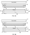
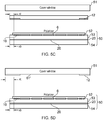
- Figs 5A, 5B , 5C and 5D illustrate some but not all of the implementations of the apparatus 2 comprising integrated display arrangement 50 and sensing arrangement 5.
- the second shield electrode 20 is implemented between the intermediary layer 53 and a bottom off the optical control layer 54.
- the optical control layer 54 may be on top of a substrate.
- the second shield electrode 20 is a dedicated electrically uniform conductive layer which is normally optically transparent or the electrode 20 is part of any suitable layers existing between the layers 53, 54.
- the first shield electrode 12 and the capacitive sensor electrodes 6 (and conductive traces 10) are in band A and the second shield electrode 20 is beneath the polarizer layer 52 in band C.
- the second shield electrode 20 is implemented on top of the polarizer layer 52, for example, as an integral part of the polarizer layer 52.
- the second shield electrode 20 is a dedicated electrically uniform conductive layer which is normally optically transparent or the electrode 20 is part of any suitable layers existing on the polarizer layer 52.
- the first shield electrode 12, the capacitive sensor electrodes 6 (and conductive traces 10) and the second shield electrode 20 are in band A.
- the first shield electrode 10 is implemented under the window 51 and above the polarizer 52.
- the capacitive sensor electrodes 6 are implemented between the polarizer layer 52 and the intermediary layer 53.
- the second shield electrode 20 is implemented between the intermediary layer 53 and a bottom of the optical control layer 54.
- the optical control layer 54 may be on top of a substrate.
- the second shield electrode 20 is a dedicated electrically uniform conductive layer which is normally optically transparent or the electrode 20 is part of any suitable layers existing between and/or including the layers 53, 54.
- the first shield electrode 12 is in band A
- the capacitive sensor electrodes 6 are in band B
- the second shield electrode 20 is beneath the polarizer layer 52, in band C.
- the separation of components into separate bands separates the components. If separation of the components is a design requirement, then this design requirement may be fulfilled without using additional separating layers.
- the first shield electrode 10 is implemented on a bottom surface 61' of a cover window 51.
- the second shield electrode 20 is implemented between the intermediary layer 53 and optical control layer 54.
- the optical control layer 54 may be on top of a substrate.
- the second shield electrode 20 is a dedicated electrically uniform conductive layer which is normally optically transparent or the electrode 20 is part of any suitable layers existing between and/or including the layers 53, 54.
- the capacitive sensor electrodes 6 (and conductive traces 10) are implemented between the polarizer layer 52 and the intermediary layer 53.
- the first shield electrode 12 is in band A
- the capacitive sensor electrodes 6 (and conductive traces 10) are in band B
- the second shield electrode 20 is beneath the polarizer layer 52, in band C.
- the capacitive sensor electrodes 6 (and conductive traces 10) and the second shield electrode 20 are physically separated by at least the thickness of the intermediary layer 53. This electrically separates the capacitive sensor electrodes 6 (and conductive traces 10) and the second shield electrode 20.
- the capacitive sensor electrodes 6 (and conductive traces 10) can therefore be formed directly on the top substrate of the display (intermediary layer 53) while retaining a required electrical separation.
- Fig 6A illustrates a touch panel module 34 that comprise the apparatus 2 an integrated display and sensing arrangement.
- the apparatus 2 is operable as a functional sensing arrangement and, with additional components, as a functional display.
- the touch panel module 34 may be used in combination with a light source 57 and a polarizer 56 to form a touch screen display.
- Fig 6B illustrates a touch sensitive display module 36 that comprises in an apparatus 2 an integrated display and sensing arrangement.
- the apparatus 2 is operable as a functional display arrangement 50 and a functional sensing arrangement 5.
- Fig 6C illustrates an electronic device 38 that at least comprises in an apparatus 2 an integrated display and sensing arrangement.
- the apparatus 2 is operable as a functional display arrangement 50 and a functional sensing arrangement 5.
- the electronic device 38 may, for example, additionally comprise a processor 39 that processes the output 27 of the detection circuitry 26.
- module' refers to a unit or apparatus that excludes certain parts/components that would be added by an end manufacturer or a user.
- Operatively connected means connected in a manner that enables the required functionality (operation). Any number or combination of intervening elements can exist (including no intervening elements) between two items that are operatively connected..
Landscapes
- Engineering & Computer Science (AREA)
- Physics & Mathematics (AREA)
- Theoretical Computer Science (AREA)
- General Engineering & Computer Science (AREA)
- General Physics & Mathematics (AREA)
- Nonlinear Science (AREA)
- Human Computer Interaction (AREA)
- Crystallography & Structural Chemistry (AREA)
- Optics & Photonics (AREA)
- Chemical & Material Sciences (AREA)
- Mathematical Physics (AREA)
- Computer Networks & Wireless Communication (AREA)
- Position Input By Displaying (AREA)
Description
- Embodiments of the present invention relate to an apparatus. In particular, they relate to an apparatus comprising a plurality of capacitive sensor electrodes distributed over a sensing area.
- Current touch sensitive displays may use a plurality of capacitive sensor electrodes distributed over a sensing area. The capacitive sensor electrodes sense a proximal grounded object such as a user's finger touching the sensing area.
US 2010/0220071 A1 discloses for example a capacitive touch panel arranged on a display and provided with shield electrodes overlying and underlying the detection electrodes. -
US2012/0081328 A1 discloses an electrode arrangement for a capacitive sensor device capable of detecting a position and/or an approach of an object. - The invention is defined in the appended claims. According to the embodiments of the invention there is provided an apparatus as claimed in the appended claims.
- According to the embodiments of the invention there is provided an apparatus comprising: a sensing arrangement comprising: an array of capacitive sensor electrodes comprising a plurality of distinct capacitive sensor electrodes distributed over a sensing area; conductive traces operatively connected to the plurality of distinct capacitive sensor electrodes; a first shield electrode overlying, in the sensing area, at least the conductive traces; a second shield electrode underlying, in the sensing area, the conductive traces and the capacitive sensor electrodes; a display arrangement comprising:
- a transparent cover
- a polarizer, underlying the transparent cover;
- an intermediary layer, underlying the polarizer;
- an optical control layer, underlying the intermediary layer;
- wherein the sensing arrangement and the display arrangement are integrated,
- the first shield electrode being positioned beneath the transparent cover and above the polarizer;
- the capacitive sensor electrodes being positioned beneath the transparent cover and beneath the first shield electrode and above the optical control layer; and
- the second shield electrode being positioned beneath the transparent cover and beneath the capacitive sensor electrodes and above the optical control layer, wherein the apparatus is configured to provide an alternating voltage to the first shield electrode and the second shield electrode.
- According to various, but not necessarily all, embodiments of the invention there is provided an apparatus comprising:
- a sensing arrangement comprising:
- an array of capacitive sensor electrodes comprising a plurality of distinct capacitive sensor electrodes distributed over a sensing area;
- conductive traces operatively connected to the plurality of distinct capacitive sensor electrodes;
- a first shield electrode overlying, in the sensing area, at least the conductive traces;
- a second shield electrode underlying, in the sensing area, the conductive traces and the capacitive sensor electrodes;
- a display arrangement comprising:
- a transparent cover;
- a polarizer, underlying the transparent cover;
- an intermediary layer, underlying the polarizer;
- an optical control layer, underlying the intermediary layer;
- wherein the sensing arrangement and the display arrangement are integrated, the first shield electrode being positioned beneath the transparent cover and above the polarizer;
- the capacitive sensor electrodes being positioned beneath the transparent cover and beneath the first shield electrode and above the optical control layer; and
- the second shield electrode being positioned beneath the transparent cover and beneath the capacitive sensor electrodes and above the optical control layer, wherein the second shield electrode is an integral part of the polarizer and wherein the apparatus is configured to provide an alternating voltage to the first shield electrode and the second shield electrodes.
- For a better understanding of various examples of embodiments of the present invention reference will now be made by way of example only to the accompanying drawings in which:
-
Fig 1 illustrates an apparatus comprising a sensing arrangement comprising a plurality of capacitive sensor electrodes distributed over a sensing area; -
Fig 2 illustrates one example of a sensing arrangement comprising a plurality of capacitive sensor electrodes distributed over a sensing area; -
Fig 3 schematically illustrates a cross-section through a sensing arrangement; -
Figs 4A to 4C illustrate examples of display arrangements; -
Fig 4D illustrates how the display arrangements ofFigs 4A to 4C may be integrated with a sensing arrangement; -
Figs 5A, 5B ,5C and 5D illustrate examples of an apparatus comprising an integrated display and sensing arrangement. -
Fig 6A illustrates a touch panel module; -
Fig 6B illustrates a touch sensitive display module; and -
Fig 6C illustrates an electronic device. - The Figures illustrate an
apparatus 2 comprising: - a
sensing arrangement 5 comprising:- an
array 4 ofcapacitive sensor electrodes 6 comprising a plurality of distinctcapacitive sensor electrodes 6 distributed over asensing area 8; -
conductive traces 10 operatively connected to the plurality of distinctcapacitive sensor electrodes 6; - a
first shield electrode 12 overlying, in thesensing area 8,conductive traces 10; and - a
second shield electrode 20 underlying, in thesensing area 8, theconductive traces 10 and thecapacitive sensor electrodes 6, and
- an
- a
display arrangement 50 comprising:- a
transparent cover 51; - a
polarizer 52, underlying thetransparent cover 51; - an
intermediary layer 53, underlying thepolarizer 52; - an
optical control layer 54, underlying theintermediary layer 53;
- a
- wherein the
sensing arrangement 5 and thedisplay arrangement 50 are integrated, - the
first shield electrode 12 being positioned beneath thetransparent cover 51 and above thepolarizer 52; - the
capacitive sensor electrodes 6 being positioned beneath thetransparent cover 51 and beneath thefirst shield electrode 12 and above theoptical control layer 54; and - the
second shield electrode 20 being positioned beneath thetransparent cover 51 and beneath thecapacitive sensor electrodes 6 and above theoptical control layer 54. -
Fig 1 illustrates anapparatus 2 comprising: asensing arrangement 5 comprising a plurality ofcapacitive sensor electrodes 6 distributed over asensing area 8 andconductive traces 10 at least partially distributed over thesensing area 8; and ashield electrode 12 partially overlying, in thesensing area 8, thesensing arrangement 5. - In this example, the
apparatus 2 overlies adisplay 40 and operates as a capacitive touch panel for thedisplay 40. Thedisplay 40 and theapparatus 2 in combination form a touch sensitive display configured to detect a variation in capacitance arising from proximity of auser input device 32 to one or more of the plurality ofsensor electrodes 6. - The
sensing arrangement 5 is configured to sense a variation in capacitance arising from proximity of auser input device 32 at or over thesensing area 8 of atouch surface 7. In this example theuser input device 32 is a user's finger. - The
apparatus 2 is configured to sense not only the (x, y) position of the user's finger within thesensing area 8 when it touches thesensing area 8 of thetouch surface 7 but may also, in this example, additionally provide a (z) position of the user's finger when it is close to but not touching thesensing area 8 of thetouch surface 7 and/or provide an (x, y) position of the user's finger when it is close to but not yet touching the sensing area of thetouch surface 7. Theapparatus 2 therefore provides for not only two-dimensional sensing but also three-dimensional sensing. - The
apparatus 2 also comprises asecond shield electrode 20 underlying, in thesensing area 8, the conductive traces 10 and thesensor electrodes 6. Thesecond shield electrode 20 may be a continuous uninterrupted electrode. - The
first shield electrode 12, the conductive traces 10, thecapacitive sensor electrodes 6 and thesecond shield electrode 20 are all positioned at least within thesensing area 8 and overlie, in this example, adisplay 40. As they overlie adisplay 40 they are preferably transparent. - The
first shield electrode 12, the conductive traces 10, thecapacitive sensor electrodes 6 and thesecond shield electrode 20 may therefore be formed from conductive and transparent material. They may be formed from the same or similar material or mixtures of material. Examples of suitable conductive and transparent materials include, for example, Indium-Tin-Oxide (ITO) , metal mesh, silver nanowires and carbon nanotube composite. -
Fig 2 illustrates one example of asensing arrangement 5 comprising
a plurality ofcapacitive sensor electrodes 6 distributed over asensing area 8 andconductive traces 10 partially distributed over thesensing area 8. The plurality ofcapacitive sensor electrodes 6 are arranged as a regular array in this example. The capacitive sensor electrodes are arranged as a N row by M column regular array, with common fixed spacing between columns and common fixed spacing between rows. - Each
capacitive sensor electrode 6 has an associatedconductive trace 10 for conveying a signal generated by thatsensor electrode 6 away from thesensor area 8. In the illustrated example, eachsensor electrode 6 and its associatedconductive trace 10 is physically connected. Thesensor electrodes 6 and the conductive traces 10 may be arranged within acommon plane 16. They may, for example, be formed by patterning a planar layer of transparent conductive material. - The
first shield electrode 12, in this example but not necessarily all examples, overlies at least portions of at least some of thesensor electrodes 6. - In the illustrated example, the
first shield electrode 12 overlies, in thesensing area 8, all of the conductive traces 10. In other examples, thefirst shield electrode 12 does not overlie, in thesensing area 8, all of the conductive traces 10 but instead overlies more than 80% of thearea 14 occupied by the conductive traces 10. - It is desirable to keep the electrical resistance of the conductive traces 10 small to reduce resistance-capacitance (RC) delays and improve measurement speed. This may be achieved by using material that has a higher conductivity and/or by making the conductive traces 10 wider. However, widening the conductive traces 10 increases the
area 14 occupied by the conductive traces 10 and may create undesirable stray capacitance effects. However this effect is reduced or eliminated by theoverlying shield electrode 12. -
Fig 3 schematically illustrates a cross-section through thesensing arrangement 5 along a line corresponding to an 'operational' capacitive sensor electrode. That is thefirst shield electrode 12 along this cross-section does not cover thecapacitive sensor electrodes 6. - The
first shield electrode 12 is operatively connected to anode 22. Operatively connected means that there is a signal path but they may or may not be directly physically connected. When theapparatus 2 is operational thenode 22 is held at a constant potential such as, for example, ground potential.Circuitry 24 is configured to provide a reference voltage signal to thefirst shield electrode 12. Thecircuitry 24 could be a simple galvanic connection to ground provided by, for example, a housing, a ground plane or a chassis. - In this example, a
second shield electrode 20 is present. It is also operatively connected to thenode 22. -
Detection circuitry 26 is operatively connected between thefirst shield electrode 12 and thearray 4 ofcapacitive sensor electrodes 6. - A
multiplexer 28 is operatively connected between thedetection circuitry 26 and thearray 4 ofcapacitive sensor electrodes 6. Themultiplexer 28 is configured to isolate, for detection, each of the plurality ofcapacitive sensor electrodes 6 of thearray 4. -
Drive circuitry 30 is configured to provide an alternating voltage to thefirst shield electrode 12 and to thesecond shield electrode 20. - The
drive circuitry 30 is configured to provide a time varying electric field at each of thesensor electrodes 6. - The
detection circuitry 26 is configured to detect a variation in capacitance arising from proximity of auser input device 32 to one or more of the plurality ofsensor electrodes 6. Thedetection circuitry 26 may comprise a low-impedance charge amplifier. - When the user's hand, or some other grounded
user input device 32, is brought to the vicinity of thesensing area 8 of theapparatus 2, a capacitive current flows from thefirst shield electrode 12 through thedetection circuitry 26 to one or morecapacitive sensor electrodes 6. The charge amplifier in thedetection circuitry 26 registers a charge displacement due to the current. The output of the charge amplifier is synchronously rectified and integrated, after which it is passed to an analog-to-digital converter and then provided asdigital output 27 for processing in the digital domain. - The drive voltage and the drive frequency typically range from 1 V to 10 V and from 10 to 200 kHz, respectively.
- Due to reasons of cost and size, a single charge amplifier and a single analog-to-digital converter may be used in the
detection circuitry 26 for multiplecapacitive sensor electrodes 6 and amultiplexer 28 may be used to isolate for sensing eachcapacitive sensor electrode 6 separately. -
Figs 4A to 4C illustrate examples ofdisplay arrangements 50 andFig 4D illustrates how the display arrangement and the previously describedsensing arrangement 5 can be integrated in anapparatus 2. -
Fig 4A illustrates ageneric display arrangement 50. Thisdisplay arrangement 50 comprises: atransparent cover 51; apolarizer 52, underlying thetransparent cover 51; anintermediary layer 53, underlying thepolarizer 52; and anoptical control layer 54, underlying theintermediary layer 53. - The
transparent cover 51 is aprotective cover 51. It may be formed from glass, plastic or other transparent material. Transparent means optically clear, that is not obscured, it does not prevent the material being colored or uncoloured. - The
optical control layer 54 is used to control the display output. - The
optical control layer 54 may, for example, be a material that modulates a property of light that is transmitted through it. For example, a liquid crystal can be used to change a polarisation state of light. - The
optical control layer 54 may, for example, be a material that is controlled to emit light in a variable manner. For example, organic light emitting diodes can be used to emit different colors or light with different intensities. - If the display arrangement is an active matrix display, then a
switching layer 55 will be present, underlying theoptical control layer 54. -
Fig 4B illustrates a specific example of the generic display arrangement illustrated inFig 4A . This specific example is a liquidcrystal display arrangement 50. - In this example, the
optical control layer 54 is a layer of liquid crystal. Theintermediary layer 53 may be used to seal and protect the nematicliquid crystal layer 54. In this example, theintermediary layer 53 is acolor filter 53. - The
switching layer 55 may comprise an array of transistors used to actively switch the local state of the nematic liquid crystal in theoptical control layer 54. The transistors may, for example, be thin film transistors. - The light
crystal display arrangement 50 illustrated is a transmissive arrangement. It comprises anunderlying light emitter 57, which transmits light through apolarizer layer 56, theswitching layer 55 and then through the overlying layers 54, 53, 52, 51. -
Fig 4C illustrates a specific example of the generic display arrangement illustrated inFig 4A . This specific example is an organic light emitting diode (OLED)display arrangement 50. - In this example, the
optical control layer 54 is a layer of organic light emitting material. Theintermediary layer 53 may be used to seal and protect the organic light emissive material. In this example, theintermediary layer 53 is an encapsulating layer. - The
switching layer 55 may comprise an array of transistors used to actively switch the local state of the organic light emissive material. The transistors may, for example, be thin film transistors. - The
OLED display arrangement 50 illustrated is an emissive arrangement. The organic light emissive material in theoptical control layer 54 selectively emits light under the control of theswitching layer 55. - As will be appreciated from the description of
Figs 1 to 3 , asensing arrangement 5 comprises: anarray 4 ofcapacitive sensor electrodes 6 comprising a plurality of distinctcapacitive sensor electrodes 6 distributed over asensing area 8; conductive traces 10 operatively connected to the plurality of distinctcapacitive sensor electrodes 6; afirst shield electrode 12 overlying, in thesensing area 8, conductive traces 10; and asecond shield electrode 20 underlying, in thesensing area 8, the conductive traces 10 and thecapacitive sensor electrodes 6. - There is a common connection between first and second shield electrode which is configured to be connected to drive
circuitry 30 and detector 26 (seeFig 3 ). -
Fig 4D illustrates how such asensing arrangement 5 may be integrated with thedisplay arrangement 50 during manufacture. -
Fig 4D illustrates positions where the components of thesensing arrangement 5 may placed among the components of thedisplay arrangement 50, while respecting the above described ordering of the components of thesensing arrangement 5. - The order is that the
first shield electrode 12 is uppermost. It is above theplane 16 occupied by the conductive traces 10 and thecapacitive sensor electrodes 6. Thesecond shield electrode 20 is lowermost. It is below theplane 16 occupied by the conductive traces 10 and thecapacitive sensor electrodes 6. - The possible positions of the components of the
sensing arrangement 5 may be divided into three distinct bands. - Band A is the space from a
bottom surface 63 of thepolarizer 52 to anupper surface 61 of thecover 51. - Band B is the space from the
bottom surface 63 of thepolarizer 52 to abottom surface 65 of theintermediary layer 53. Bands A and B overlap only at thebottom surface 63 of the polarizer. - Band C is the space from the
bottom surface 65 of theintermediary layer 53 and above a bottom surface of theoptical control layer 54. Bands B and C overlap only at thebottom surface 65 of theintermediary layer 53. - The possible positions of the
first shield electrode 12 of thesensing arrangement 5 are illustrated using the label P12. The first shield electrode is positioned within band A. - The
first shield electrode 12 may be attached to thetransparent cover 51 either directly or indirectly, for example, by depositing conductive material on an upper side 61 (or under side 61') of thetransparent cover 51 or for example by adhering thefirst shield electrode 12 to the upper side 61 (or under side 61') of thetransparent cover 51, either directly or indirectly, using optically transparent material. - The
first shield electrode 12 may be attached to thepolarizer 52 either directly or indirectly, for example, by depositing conductive material on an upper side 62 (or under side 63) of thepolarizer 52 or for example by adhering thefirst shield electrode 12 to the upper side 62 (or under side 63) of thepolarizer 52, either directly or indirectly, using optically transparent material. - The possible positions of the capacitive sensor electrodes 6 (and conductive traces 10) of the
sensing arrangement 5 are illustrated using the label P6. The capacitive sensor electrodes 6 (and conductive traces 10) are positioned within band A or band B or band C. - When positioned within band A, the capacitive sensor electrodes 6 (and conductive traces 10) may be attached to the
polarizer 52 either directly or indirectly, for example, by depositing conductive material on an upper side 62 (or under side 63) of thepolarizer 52 or for example by adhering the capacitive sensor electrodes 6 (and conductive traces 10) to the upper side 62 (or under side 62) of thepolarizer 52, either directly or indirectly, using optically transparent material. - When positioned within band B, the capacitive sensor electrodes 6 (and conductive traces 10) may be attached to the
polarizer layer 52 either directly or indirectly, for example, by depositing conductive material on an underside 63 of thepolarizer layer 52 or for example by adhering the capacitive sensor electrodes 6 (and conductive traces 10) to theunder side 63 of thepolarizer layer 52, either directly or indirectly, using optically transparent material. - When positioned within band B, the capacitive sensor electrodes 6 (and conductive traces 10) may be attached to the
intermediary layer 53 either directly or indirectly, for example, by depositing conductive material on an upper side 64 (or under side 65) of theintermediary layer 53 or for example by adhering the capacitive sensor electrodes 6 (and conductive traces 10) to the upper side 64 (or under side 65) of theintermediary layer 53, either directly or indirectly, using optically transparent material. - When positioned within band C, the capacitive sensor electrodes 6 (and conductive traces 10) may be attached to the
intermediary layer 53 either directly or indirectly, for example, by depositing conductive material on an underside 65 of theintermediary layer 53 or for example by adhering the capacitive sensor electrodes 6 (and conductive traces 10) to theunder side 65 of theintermediary layer 53, either directly or indirectly, using optically transparent material. - The possible positions of the
second shield electrode 20 of thesensing arrangement 5 are illustrated using the label P20. Thesecond shield electrode 20 is positioned within band A or band B or band C. In some embodiments, thesecond shield electrode 20 is positioned only within band B or band C. - When positioned within band A, the
second shield electrode 20 may be attached to thepolarizer 52 either directly or indirectly, for example, by depositing conductive material on anupper side 62 of thepolarizer 52 or for example by adhering thesecond shield electrode 20 to theupper side 62 of thepolarizer 52, either directly or indirectly, using optically transparent material. - When positioned within band B, the
second shield electrode 20 may be attached to thepolarizer layer 52 either directly or indirectly, for example, by depositing conductive material on an underside 63 of thepolarizer layer 52 or for example by adhering thesecond shield electrode 20 to theunder side 63 of thepolarizer layer 52, either directly or indirectly, using optically transparent material. - When positioned within band B, the
second shield electrode 20 may be attached tointermediary layer 53 either directly or indirectly, for example, by depositing conductive material on an upper side 64 (or lower side 65) of theintermediary layer 53 or for example by adhering thesecond shield electrode 20 to the upper side 64 (or lower side 65) of theintermediary layer 53, either directly or indirectly, using optically transparent material. - When positioned within band C, the
second shield electrode 20 may be attached to theintermediary layer 53 either directly or indirectly, for example, by depositing conductive material on an underside 65 of theintermediary layer 53 or for example by adhering thesecond shield electrode 20 to theunder side 65 of theintermediary layer 53, either directly or indirectly, using optically transparent material. - It will therefore be appreciated from the foregoing that the
first shield electrode 12 may be positioned above theintermediary layer 53; thecapacitive sensor electrodes 6 may be positioned beneath thetransparent cover 51 and beneath thefirst shield electrode 12 and above theoptical control layer 54; and thesecond shield electrode 20 may be positioned beneath the transparent cover 51 (e.g. beneath the polarizer layer 52) and beneath thecapacitive sensor electrodes 6 and above theoptical control layer 54/switching layer 55. -
Figs 5A, 5B ,5C and 5D illustrate some but not all of the implementations of theapparatus 2 comprising integrateddisplay arrangement 50 andsensing arrangement 5. - In each of
Figs 5A, 5B ,5C and 5D , the conductive traces 10 are overlapped by the overlyingfirst shield electrode 12. - In
Fig 5A , thesecond shield electrode 20 is implemented between theintermediary layer 53 and a bottom off theoptical control layer 54. Theoptical control layer 54 may be on top of a substrate. Thesecond shield electrode 20 is a dedicated electrically uniform conductive layer which is normally optically transparent or theelectrode 20 is part of any suitable layers existing between thelayers Fig 5A , thefirst shield electrode 12 and the capacitive sensor electrodes 6 (and conductive traces 10) are in band A and thesecond shield electrode 20 is beneath thepolarizer layer 52 in band C. - In
Fig 5B , thesecond shield electrode 20 is implemented on top of thepolarizer layer 52, for example, as an integral part of thepolarizer layer 52. Thesecond shield electrode 20 is a dedicated electrically uniform conductive layer which is normally optically transparent or theelectrode 20 is part of any suitable layers existing on thepolarizer layer 52. InFig 5B , thefirst shield electrode 12, the capacitive sensor electrodes 6 (and conductive traces 10) and thesecond shield electrode 20 are in band A. - In
Fig 5C , thefirst shield electrode 10 is implemented under thewindow 51 and above thepolarizer 52. The capacitive sensor electrodes 6 (and conductive traces 10) are implemented between thepolarizer layer 52 and theintermediary layer 53. Thesecond shield electrode 20 is implemented between theintermediary layer 53 and a bottom of theoptical control layer 54. Theoptical control layer 54 may be on top of a substrate. Thesecond shield electrode 20 is a dedicated electrically uniform conductive layer which is normally optically transparent or theelectrode 20 is part of any suitable layers existing between and/or including thelayers - In
Fig 5C , thefirst shield electrode 12 is in band A, the capacitive sensor electrodes 6 (and conductive traces 10) are in band B and thesecond shield electrode 20 is beneath thepolarizer layer 52, in band C. The separation of components into separate bands separates the components. If separation of the components is a design requirement, then this design requirement may be fulfilled without using additional separating layers. - In
Fig 5D , thefirst shield electrode 10 is implemented on a bottom surface 61' of acover window 51. Thesecond shield electrode 20 is implemented between theintermediary layer 53 andoptical control layer 54. Theoptical control layer 54 may be on top of a substrate. Thesecond shield electrode 20 is a dedicated electrically uniform conductive layer which is normally optically transparent or theelectrode 20 is part of any suitable layers existing between and/or including thelayers polarizer layer 52 and theintermediary layer 53. InFig 5D , thefirst shield electrode 12 is in band A, the capacitive sensor electrodes 6 (and conductive traces 10) are in band B and thesecond shield electrode 20 is beneath thepolarizer layer 52, in band C. - In
Figs 5A ,5C and 5D , where thesecond shield electrode 20 is positioned under theintermediate layer 53 and the capacitive sensor electrodes 6 (and conductive traces 10) are positioned above theintermediate layer 53, the capacitive sensor electrodes 6 (and conductive traces 10) and thesecond shield electrode 20 are physically separated by at least the thickness of theintermediary layer 53. This electrically separates the capacitive sensor electrodes 6 (and conductive traces 10) and thesecond shield electrode 20. The capacitive sensor electrodes 6 (and conductive traces 10) can therefore be formed directly on the top substrate of the display (intermediary layer 53) while retaining a required electrical separation. -
Fig 6A illustrates atouch panel module 34 that comprise theapparatus 2 an integrated display and sensing arrangement. Theapparatus 2 is operable as a functional sensing arrangement and, with additional components, as a functional display. Thetouch panel module 34 may be used in combination with alight source 57 and apolarizer 56 to form a touch screen display. -
Fig 6B illustrates a touchsensitive display module 36 that comprises in anapparatus 2 an integrated display and sensing arrangement. Theapparatus 2 is operable as afunctional display arrangement 50 and afunctional sensing arrangement 5. -
Fig 6C illustrates anelectronic device 38 that at least comprises in anapparatus 2 an integrated display and sensing arrangement. Theapparatus 2 is operable as afunctional display arrangement 50 and afunctional sensing arrangement 5. Theelectronic device 38 may, for example, additionally comprise aprocessor 39 that processes theoutput 27 of thedetection circuitry 26. - As used here 'module' refers to a unit or apparatus that excludes certain parts/components that would be added by an end manufacturer or a user.
- Operatively connected means connected in a manner that enables the required functionality (operation). Any number or combination of intervening elements can exist (including no intervening elements) between two items that are operatively connected..
- Although embodiments of the present invention have been described in the preceding paragraphs with reference to various examples, it should be appreciated that modifications to the examples given can be made without departing from the scope of the invention as claimed.
- Features described in the preceding description may be used in combinations other than the combinations explicitly described.
- Although functions have been described with reference to certain features, those functions may be performable by other features whether described or not.
- Although features have been described with reference to certain embodiments, those features may also be present in other embodiments whether described or not.
- Whilst endeavoring in the foregoing specification to draw attention to those features of the invention believed to be of particular importance it should be understood that the Applicant claims protection in respect of any patentable feature or combination of features defined in the appended claims.
Claims (14)
- An apparatus (2) comprising:a sensing arrangement (5) comprising:an array (4) of capacitive sensor electrodes (6) comprising a plurality of distinct capacitive sensor electrodes distributed over a sensing area (8);conductive traces (10) operatively connected to the plurality of distinct capacitive sensor electrodes;a first shield electrode (12) overlying, in the sensing area, at least the conductive traces;a second shield electrode (20) underlying, in the sensing area, the conductive traces and the capacitive sensor electrodes;a display arrangement (50) comprising:a transparent cover;a polarizer (52), underlying the transparent cover (51);an intermediary layer (53), underlying the polarizer;an optical control layer (54) configured to control output of the display arrangement, underlying the intermediary layer;wherein the sensing arrangement and the display arrangement are integrated, the first shield electrode being positioned beneath the transparent cover and above the polarizer;the capacitive sensor electrodes being positioned beneath the transparent cover and beneath the first shield electrode and above the optical control layer;the second shield electrode being positioned beneath the transparent cover and beneath the capacitive sensor electrodes and above the optical control layer; and
wherein the apparatus is configured to provide an alternating voltage to the first shield electrode and the second shield electrode. - An apparatus as claimed in claim 1, wherein the capacitive sensor electrodes are positioned beneath the polarizer and the second shield electrode is positioned beneath the intermediary layer.
- An apparatus as claimed in claim 1, wherein the second shield electrode is positioned beneath the polarizer and beneath the capacitive sensor electrodes and wherein the second shield electrode is positioned above the intermediary layer or wherein the second shield electrode is positioned beneath the intermediary layer.
- An apparatus as claimed in any preceding claim, wherein the second shield electrode is attached to the polarizer or attached to the intermediary layer.
- An apparatus as claimed in any preceding claim, wherein the capacitive sensor electrodes are positioned beneath the transparent cover and beneath the first shield electrode and are positioned above the intermediary layer or above the polarizer or beneath the polarizer and above the intermediary layer.
- An apparatus as claimed in any preceding claim, wherein the capacitive sensor electrodes are attached to the polarizer or attached to the intermediary layer.
- An apparatus as claimed in any preceding claim, wherein the first shield electrode is attached to the transparent cover or attached to the polarizer.
- An apparatus as claimed in any preceding claim, comprising a common connection between first and second shield electrode.
- An apparatus as claimed in any preceding claim, wherein the second shield electrode is a continuous uninterrupted electrode and/or wherein the first shield electrode overlies, in the sensing area, more than 80% of the area occupied by the conductive traces.
- An apparatus as claimed in any preceding claim, wherein the sensor electrodes and the conductive traces are arranged within a common plane and/or wherein the sensor electrodes, the conductive traces and the second shield electrode are transparent.
- An apparatus as claimed in any preceding claim, comprising detection circuitry (26) connected between the first shield electrode and a multiplexer (28) connected to the array of capacitive sensor electrodes, wherein the multiplexer is configured to isolate, for detection, each of the plurality of capacitive sensor electrodes of the array.
- An apparatus as claimed in claim 11, wherein the detection circuitry comprises a low-impedance charge amplifier.
- An apparatus as claimed in any preceding claim, comprising drive circuitry (30) configured to provide a time varying electric field at each of the sensor electrodes and detection circuitry configured to detect a variation in capacitance arising from proximity of a user input device (32) to one or more of the plurality of sensor electrodes.
- An apparatus as claimed in any preceding claim embodied as a touch panel module (34) or a touch sensitive display module (36) or an electronic device (38).
Applications Claiming Priority (2)
| Application Number | Priority Date | Filing Date | Title |
|---|---|---|---|
| US13/758,039 US9348453B2 (en) | 2013-02-04 | 2013-02-04 | Touch sensing arrangement with first and second shield electrodes |
| PCT/IB2014/058758 WO2014118759A1 (en) | 2013-02-04 | 2014-02-03 | Capacitive sensor integrated in a display device |
Publications (2)
| Publication Number | Publication Date |
|---|---|
| EP2951636A1 EP2951636A1 (en) | 2015-12-09 |
| EP2951636B1 true EP2951636B1 (en) | 2018-04-11 |
Family
ID=50184959
Family Applications (1)
| Application Number | Title | Priority Date | Filing Date |
|---|---|---|---|
| EP14706953.8A Active EP2951636B1 (en) | 2013-02-04 | 2014-02-03 | Capacitive sensor integrated in a display device |
Country Status (3)
| Country | Link |
|---|---|
| US (1) | US9348453B2 (en) |
| EP (1) | EP2951636B1 (en) |
| WO (1) | WO2014118759A1 (en) |
Families Citing this family (16)
| Publication number | Priority date | Publication date | Assignee | Title |
|---|---|---|---|---|
| KR102023436B1 (en) * | 2013-01-30 | 2019-09-20 | 엘지디스플레이 주식회사 | Apparatus for display including touch electrode |
| GB2518627A (en) * | 2013-09-25 | 2015-04-01 | Nokia Technologies Oy | An apparatus |
| GB2521830A (en) * | 2014-01-02 | 2015-07-08 | Nokia Technologies Oy | An apparatus and/or method |
| DE102014217237B4 (en) | 2014-08-28 | 2025-07-10 | HELLA GmbH & Co. KGaA | Lighting device and method for producing a lighting device |
| US20160188072A1 (en) * | 2014-12-29 | 2016-06-30 | Shenzhen China Star Optoelectronics Technology Co., Ltd. | Touch display panel |
| KR102350084B1 (en) * | 2015-01-15 | 2022-01-11 | 삼성디스플레이 주식회사 | Touch panel and display device using the same |
| CN105045452B (en) * | 2015-08-19 | 2018-01-30 | 深圳市华星光电技术有限公司 | One kind touches display device and its array base palte |
| US10275063B2 (en) | 2016-05-26 | 2019-04-30 | Japan Display Inc. | Display device and sensor |
| US10528172B2 (en) | 2016-06-17 | 2020-01-07 | Microsoft Technology Licensing, Llc | Pressure sensor for display devices |
| JP6739556B2 (en) * | 2016-06-30 | 2020-08-12 | コーニンクレッカ フィリップス エヌ ヴェKoninklijke Philips N.V. | Sealed control panel for medical devices |
| KR102564349B1 (en) * | 2016-09-30 | 2023-08-04 | 엘지디스플레이 주식회사 | Organic light emitting display apparatus |
| KR102630256B1 (en) * | 2016-09-30 | 2024-01-25 | 엘지디스플레이 주식회사 | Organic light emitting display apparatus |
| JP6734771B2 (en) * | 2016-12-28 | 2020-08-05 | 株式会社ジャパンディスプレイ | Display device |
| CN107170780A (en) * | 2017-05-17 | 2017-09-15 | 京东方科技集团股份有限公司 | OLED display panel and preparation method thereof, OLED display |
| CN107275460A (en) * | 2017-07-12 | 2017-10-20 | 惠州市聚飞光电有限公司 | A kind of luminous LED component of one side and method for packing |
| CN108052220B (en) * | 2017-12-06 | 2021-11-26 | 京东方科技集团股份有限公司 | Display module, manufacturing method thereof, display device and wearable device |
Family Cites Families (20)
| Publication number | Priority date | Publication date | Assignee | Title |
|---|---|---|---|---|
| JP2001075074A (en) | 1999-08-18 | 2001-03-23 | Internatl Business Mach Corp <Ibm> | Touch sensor type liquid crystal display device |
| EP1788473A1 (en) | 2005-11-18 | 2007-05-23 | Siemens Aktiengesellschaft | input device |
| EP2027528B1 (en) | 2006-06-09 | 2012-08-01 | Apple Inc. | Touch screen liquid crystal display |
| US8040326B2 (en) | 2007-06-13 | 2011-10-18 | Apple Inc. | Integrated in-plane switching display and touch sensor |
| JP5264249B2 (en) * | 2008-03-31 | 2013-08-14 | 三菱自動車工業株式会社 | Capacitive touch sensor device |
| US8552936B2 (en) | 2008-09-08 | 2013-10-08 | Koninklijke Philips N.V. | OLED device with capacitive proximity sensing means |
| US7995041B2 (en) | 2009-02-02 | 2011-08-09 | Apple Inc. | Integrated touch screen |
| JP5337061B2 (en) | 2009-02-20 | 2013-11-06 | セイコーインスツル株式会社 | Touch panel and display device including the same |
| US20100214247A1 (en) * | 2009-02-20 | 2010-08-26 | Acrosense Technology Co., Ltd. | Capacitive Touch Panel |
| US8624849B2 (en) | 2009-04-20 | 2014-01-07 | Apple Inc. | Touch actuated sensor configuration integrated with an OLED structure |
| EP2300900B1 (en) | 2009-06-24 | 2018-09-05 | Microchip Technology Germany GmbH | Electrode arrangement for display device |
| US9323398B2 (en) * | 2009-07-10 | 2016-04-26 | Apple Inc. | Touch and hover sensing |
| CN102687103B (en) | 2009-10-28 | 2016-04-20 | 伊英克公司 | Electro-optic display with touch sensor |
| EP2339433A1 (en) | 2009-12-28 | 2011-06-29 | Holylite Microelectronics Corporation | Liquid crystal display system integrated with touch detector |
| US8692948B2 (en) * | 2010-05-21 | 2014-04-08 | Apple Inc. | Electric field shielding for in-cell touch type thin-film-transistor liquid crystal displays |
| US9470941B2 (en) * | 2011-08-19 | 2016-10-18 | Apple Inc. | In-cell or on-cell touch sensor with color filter on array |
| KR101848274B1 (en) * | 2011-09-29 | 2018-04-13 | 주식회사 지2터치 | Touch detecting means, method and touch screen panel using driving back, and display device embedding said the touch screen panel |
| US8711292B2 (en) * | 2011-11-22 | 2014-04-29 | Atmel Corporation | Integrated touch screen |
| WO2013109698A1 (en) * | 2012-01-17 | 2013-07-25 | Apple Inc. | Fingerprint sensor having pixel sensing circuitry for coupling electrodes and pixel sensing traces and related method |
| CN103294238A (en) * | 2012-03-01 | 2013-09-11 | 瀚宇彩晶股份有限公司 | Touch control display device |
-
2013
- 2013-02-04 US US13/758,039 patent/US9348453B2/en active Active
-
2014
- 2014-02-03 EP EP14706953.8A patent/EP2951636B1/en active Active
- 2014-02-03 WO PCT/IB2014/058758 patent/WO2014118759A1/en not_active Ceased
Also Published As
| Publication number | Publication date |
|---|---|
| EP2951636A1 (en) | 2015-12-09 |
| US20140218328A1 (en) | 2014-08-07 |
| WO2014118759A1 (en) | 2014-08-07 |
| US9348453B2 (en) | 2016-05-24 |
Similar Documents
| Publication | Publication Date | Title |
|---|---|---|
| US9348453B2 (en) | Touch sensing arrangement with first and second shield electrodes | |
| US9411474B2 (en) | Shield electrode overlying portions of capacitive sensor electrodes | |
| TWI686729B (en) | Display device including touch sensor and manufacturing method thereof | |
| US10331263B2 (en) | OLED display panel with touch sensing electrodes | |
| JP6581927B2 (en) | Detection device, display device, and electronic device | |
| US8692950B2 (en) | Display panel including a soft key | |
| KR102161743B1 (en) | Touch sensing device and display device comprising the same | |
| KR102350084B1 (en) | Touch panel and display device using the same | |
| KR102262470B1 (en) | Touch screen panel manufacturing method | |
| JP7466030B2 (en) | Display device | |
| JP6133732B2 (en) | Input device and detection method thereof | |
| KR20150045288A (en) | Touch panel | |
| EP2920676B1 (en) | A capacitive sensing apparatus comprising an active touch sensitive matrix and shield electrodes | |
| KR20150019130A (en) | Touch screen panel, display device comprising the same | |
| JP7466015B2 (en) | Display device | |
| KR102678327B1 (en) | Touch display apparatus | |
| EP2994816B1 (en) | Touch sensor array and method therefor | |
| JP6648834B2 (en) | Display device | |
| JP2012003768A (en) | Touch type transparent keyboard | |
| US20140285735A1 (en) | Touch display apparatus | |
| KR101736931B1 (en) | In-cell type touch display device |
Legal Events
| Date | Code | Title | Description |
|---|---|---|---|
| PUAI | Public reference made under article 153(3) epc to a published international application that has entered the european phase |
Free format text: ORIGINAL CODE: 0009012 |
|
| 17P | Request for examination filed |
Effective date: 20150904 |
|
| AK | Designated contracting states |
Kind code of ref document: A1 Designated state(s): AL AT BE BG CH CY CZ DE DK EE ES FI FR GB GR HR HU IE IS IT LI LT LU LV MC MK MT NL NO PL PT RO RS SE SI SK SM TR |
|
| AX | Request for extension of the european patent |
Extension state: BA ME |
|
| DAX | Request for extension of the european patent (deleted) | ||
| STAA | Information on the status of an ep patent application or granted ep patent |
Free format text: STATUS: EXAMINATION IS IN PROGRESS |
|
| 17Q | First examination report despatched |
Effective date: 20161107 |
|
| GRAP | Despatch of communication of intention to grant a patent |
Free format text: ORIGINAL CODE: EPIDOSNIGR1 |
|
| STAA | Information on the status of an ep patent application or granted ep patent |
Free format text: STATUS: GRANT OF PATENT IS INTENDED |
|
| INTG | Intention to grant announced |
Effective date: 20171018 |
|
| GRAJ | Information related to disapproval of communication of intention to grant by the applicant or resumption of examination proceedings by the epo deleted |
Free format text: ORIGINAL CODE: EPIDOSDIGR1 |
|
| STAA | Information on the status of an ep patent application or granted ep patent |
Free format text: STATUS: EXAMINATION IS IN PROGRESS |
|
| GRAR | Information related to intention to grant a patent recorded |
Free format text: ORIGINAL CODE: EPIDOSNIGR71 |
|
| GRAS | Grant fee paid |
Free format text: ORIGINAL CODE: EPIDOSNIGR3 |
|
| STAA | Information on the status of an ep patent application or granted ep patent |
Free format text: STATUS: GRANT OF PATENT IS INTENDED |
|
| GRAA | (expected) grant |
Free format text: ORIGINAL CODE: 0009210 |
|
| STAA | Information on the status of an ep patent application or granted ep patent |
Free format text: STATUS: THE PATENT HAS BEEN GRANTED |
|
| INTC | Intention to grant announced (deleted) | ||
| INTG | Intention to grant announced |
Effective date: 20180301 |
|
| AK | Designated contracting states |
Kind code of ref document: B1 Designated state(s): AL AT BE BG CH CY CZ DE DK EE ES FI FR GB GR HR HU IE IS IT LI LT LU LV MC MK MT NL NO PL PT RO RS SE SI SK SM TR |
|
| REG | Reference to a national code |
Ref country code: GB Ref legal event code: FG4D |
|
| REG | Reference to a national code |
Ref country code: CH Ref legal event code: EP |
|
| REG | Reference to a national code |
Ref country code: AT Ref legal event code: REF Ref document number: 988663 Country of ref document: AT Kind code of ref document: T Effective date: 20180415 |
|
| REG | Reference to a national code |
Ref country code: IE Ref legal event code: FG4D |
|
| REG | Reference to a national code |
Ref country code: DE Ref legal event code: R096 Ref document number: 602014023668 Country of ref document: DE |
|
| REG | Reference to a national code |
Ref country code: NL Ref legal event code: MP Effective date: 20180411 |
|
| REG | Reference to a national code |
Ref country code: LT Ref legal event code: MG4D |
|
| PG25 | Lapsed in a contracting state [announced via postgrant information from national office to epo] |
Ref country code: NL Free format text: LAPSE BECAUSE OF FAILURE TO SUBMIT A TRANSLATION OF THE DESCRIPTION OR TO PAY THE FEE WITHIN THE PRESCRIBED TIME-LIMIT Effective date: 20180411 |
|
| PG25 | Lapsed in a contracting state [announced via postgrant information from national office to epo] |
Ref country code: ES Free format text: LAPSE BECAUSE OF FAILURE TO SUBMIT A TRANSLATION OF THE DESCRIPTION OR TO PAY THE FEE WITHIN THE PRESCRIBED TIME-LIMIT Effective date: 20180411 Ref country code: LT Free format text: LAPSE BECAUSE OF FAILURE TO SUBMIT A TRANSLATION OF THE DESCRIPTION OR TO PAY THE FEE WITHIN THE PRESCRIBED TIME-LIMIT Effective date: 20180411 Ref country code: PL Free format text: LAPSE BECAUSE OF FAILURE TO SUBMIT A TRANSLATION OF THE DESCRIPTION OR TO PAY THE FEE WITHIN THE PRESCRIBED TIME-LIMIT Effective date: 20180411 Ref country code: FI Free format text: LAPSE BECAUSE OF FAILURE TO SUBMIT A TRANSLATION OF THE DESCRIPTION OR TO PAY THE FEE WITHIN THE PRESCRIBED TIME-LIMIT Effective date: 20180411 Ref country code: BG Free format text: LAPSE BECAUSE OF FAILURE TO SUBMIT A TRANSLATION OF THE DESCRIPTION OR TO PAY THE FEE WITHIN THE PRESCRIBED TIME-LIMIT Effective date: 20180711 Ref country code: NO Free format text: LAPSE BECAUSE OF FAILURE TO SUBMIT A TRANSLATION OF THE DESCRIPTION OR TO PAY THE FEE WITHIN THE PRESCRIBED TIME-LIMIT Effective date: 20180711 Ref country code: SE Free format text: LAPSE BECAUSE OF FAILURE TO SUBMIT A TRANSLATION OF THE DESCRIPTION OR TO PAY THE FEE WITHIN THE PRESCRIBED TIME-LIMIT Effective date: 20180411 Ref country code: AL Free format text: LAPSE BECAUSE OF FAILURE TO SUBMIT A TRANSLATION OF THE DESCRIPTION OR TO PAY THE FEE WITHIN THE PRESCRIBED TIME-LIMIT Effective date: 20180411 |
|
| PG25 | Lapsed in a contracting state [announced via postgrant information from national office to epo] |
Ref country code: RS Free format text: LAPSE BECAUSE OF FAILURE TO SUBMIT A TRANSLATION OF THE DESCRIPTION OR TO PAY THE FEE WITHIN THE PRESCRIBED TIME-LIMIT Effective date: 20180411 Ref country code: GR Free format text: LAPSE BECAUSE OF FAILURE TO SUBMIT A TRANSLATION OF THE DESCRIPTION OR TO PAY THE FEE WITHIN THE PRESCRIBED TIME-LIMIT Effective date: 20180712 Ref country code: HR Free format text: LAPSE BECAUSE OF FAILURE TO SUBMIT A TRANSLATION OF THE DESCRIPTION OR TO PAY THE FEE WITHIN THE PRESCRIBED TIME-LIMIT Effective date: 20180411 Ref country code: LV Free format text: LAPSE BECAUSE OF FAILURE TO SUBMIT A TRANSLATION OF THE DESCRIPTION OR TO PAY THE FEE WITHIN THE PRESCRIBED TIME-LIMIT Effective date: 20180411 |
|
| REG | Reference to a national code |
Ref country code: AT Ref legal event code: MK05 Ref document number: 988663 Country of ref document: AT Kind code of ref document: T Effective date: 20180411 |
|
| PG25 | Lapsed in a contracting state [announced via postgrant information from national office to epo] |
Ref country code: PT Free format text: LAPSE BECAUSE OF FAILURE TO SUBMIT A TRANSLATION OF THE DESCRIPTION OR TO PAY THE FEE WITHIN THE PRESCRIBED TIME-LIMIT Effective date: 20180813 |
|
| REG | Reference to a national code |
Ref country code: DE Ref legal event code: R097 Ref document number: 602014023668 Country of ref document: DE |
|
| PG25 | Lapsed in a contracting state [announced via postgrant information from national office to epo] |
Ref country code: SK Free format text: LAPSE BECAUSE OF FAILURE TO SUBMIT A TRANSLATION OF THE DESCRIPTION OR TO PAY THE FEE WITHIN THE PRESCRIBED TIME-LIMIT Effective date: 20180411 Ref country code: RO Free format text: LAPSE BECAUSE OF FAILURE TO SUBMIT A TRANSLATION OF THE DESCRIPTION OR TO PAY THE FEE WITHIN THE PRESCRIBED TIME-LIMIT Effective date: 20180411 Ref country code: CZ Free format text: LAPSE BECAUSE OF FAILURE TO SUBMIT A TRANSLATION OF THE DESCRIPTION OR TO PAY THE FEE WITHIN THE PRESCRIBED TIME-LIMIT Effective date: 20180411 Ref country code: DK Free format text: LAPSE BECAUSE OF FAILURE TO SUBMIT A TRANSLATION OF THE DESCRIPTION OR TO PAY THE FEE WITHIN THE PRESCRIBED TIME-LIMIT Effective date: 20180411 Ref country code: EE Free format text: LAPSE BECAUSE OF FAILURE TO SUBMIT A TRANSLATION OF THE DESCRIPTION OR TO PAY THE FEE WITHIN THE PRESCRIBED TIME-LIMIT Effective date: 20180411 Ref country code: AT Free format text: LAPSE BECAUSE OF FAILURE TO SUBMIT A TRANSLATION OF THE DESCRIPTION OR TO PAY THE FEE WITHIN THE PRESCRIBED TIME-LIMIT Effective date: 20180411 |
|
| PLBE | No opposition filed within time limit |
Free format text: ORIGINAL CODE: 0009261 |
|
| STAA | Information on the status of an ep patent application or granted ep patent |
Free format text: STATUS: NO OPPOSITION FILED WITHIN TIME LIMIT |
|
| PG25 | Lapsed in a contracting state [announced via postgrant information from national office to epo] |
Ref country code: SM Free format text: LAPSE BECAUSE OF FAILURE TO SUBMIT A TRANSLATION OF THE DESCRIPTION OR TO PAY THE FEE WITHIN THE PRESCRIBED TIME-LIMIT Effective date: 20180411 Ref country code: IT Free format text: LAPSE BECAUSE OF FAILURE TO SUBMIT A TRANSLATION OF THE DESCRIPTION OR TO PAY THE FEE WITHIN THE PRESCRIBED TIME-LIMIT Effective date: 20180411 |
|
| 26N | No opposition filed |
Effective date: 20190114 |
|
| PG25 | Lapsed in a contracting state [announced via postgrant information from national office to epo] |
Ref country code: SI Free format text: LAPSE BECAUSE OF FAILURE TO SUBMIT A TRANSLATION OF THE DESCRIPTION OR TO PAY THE FEE WITHIN THE PRESCRIBED TIME-LIMIT Effective date: 20180411 |
|
| REG | Reference to a national code |
Ref country code: CH Ref legal event code: PL |
|
| GBPC | Gb: european patent ceased through non-payment of renewal fee |
Effective date: 20190203 |
|
| PG25 | Lapsed in a contracting state [announced via postgrant information from national office to epo] |
Ref country code: LU Free format text: LAPSE BECAUSE OF NON-PAYMENT OF DUE FEES Effective date: 20190203 Ref country code: MC Free format text: LAPSE BECAUSE OF FAILURE TO SUBMIT A TRANSLATION OF THE DESCRIPTION OR TO PAY THE FEE WITHIN THE PRESCRIBED TIME-LIMIT Effective date: 20180411 |
|
| REG | Reference to a national code |
Ref country code: BE Ref legal event code: MM Effective date: 20190228 |
|
| REG | Reference to a national code |
Ref country code: IE Ref legal event code: MM4A |
|
| PG25 | Lapsed in a contracting state [announced via postgrant information from national office to epo] |
Ref country code: CH Free format text: LAPSE BECAUSE OF NON-PAYMENT OF DUE FEES Effective date: 20190228 Ref country code: LI Free format text: LAPSE BECAUSE OF NON-PAYMENT OF DUE FEES Effective date: 20190228 |
|
| PG25 | Lapsed in a contracting state [announced via postgrant information from national office to epo] |
Ref country code: GB Free format text: LAPSE BECAUSE OF NON-PAYMENT OF DUE FEES Effective date: 20190203 Ref country code: IE Free format text: LAPSE BECAUSE OF NON-PAYMENT OF DUE FEES Effective date: 20190203 |
|
| PG25 | Lapsed in a contracting state [announced via postgrant information from national office to epo] |
Ref country code: BE Free format text: LAPSE BECAUSE OF NON-PAYMENT OF DUE FEES Effective date: 20190228 Ref country code: FR Free format text: LAPSE BECAUSE OF NON-PAYMENT OF DUE FEES Effective date: 20190228 |
|
| PG25 | Lapsed in a contracting state [announced via postgrant information from national office to epo] |
Ref country code: TR Free format text: LAPSE BECAUSE OF FAILURE TO SUBMIT A TRANSLATION OF THE DESCRIPTION OR TO PAY THE FEE WITHIN THE PRESCRIBED TIME-LIMIT Effective date: 20180411 |
|
| PG25 | Lapsed in a contracting state [announced via postgrant information from national office to epo] |
Ref country code: MT Free format text: LAPSE BECAUSE OF NON-PAYMENT OF DUE FEES Effective date: 20190203 |
|
| PG25 | Lapsed in a contracting state [announced via postgrant information from national office to epo] |
Ref country code: CY Free format text: LAPSE BECAUSE OF FAILURE TO SUBMIT A TRANSLATION OF THE DESCRIPTION OR TO PAY THE FEE WITHIN THE PRESCRIBED TIME-LIMIT Effective date: 20180411 |
|
| PG25 | Lapsed in a contracting state [announced via postgrant information from national office to epo] |
Ref country code: IS Free format text: LAPSE BECAUSE OF FAILURE TO SUBMIT A TRANSLATION OF THE DESCRIPTION OR TO PAY THE FEE WITHIN THE PRESCRIBED TIME-LIMIT Effective date: 20180811 |
|
| PG25 | Lapsed in a contracting state [announced via postgrant information from national office to epo] |
Ref country code: HU Free format text: LAPSE BECAUSE OF FAILURE TO SUBMIT A TRANSLATION OF THE DESCRIPTION OR TO PAY THE FEE WITHIN THE PRESCRIBED TIME-LIMIT; INVALID AB INITIO Effective date: 20140203 |
|
| PG25 | Lapsed in a contracting state [announced via postgrant information from national office to epo] |
Ref country code: MK Free format text: LAPSE BECAUSE OF FAILURE TO SUBMIT A TRANSLATION OF THE DESCRIPTION OR TO PAY THE FEE WITHIN THE PRESCRIBED TIME-LIMIT Effective date: 20180411 |
|
| PGFP | Annual fee paid to national office [announced via postgrant information from national office to epo] |
Ref country code: DE Payment date: 20251230 Year of fee payment: 13 |