EP2950434A1 - Output filter with interphase reactor for paralleled inverters - Google Patents
Output filter with interphase reactor for paralleled inverters Download PDFInfo
- Publication number
- EP2950434A1 EP2950434A1 EP15169118.5A EP15169118A EP2950434A1 EP 2950434 A1 EP2950434 A1 EP 2950434A1 EP 15169118 A EP15169118 A EP 15169118A EP 2950434 A1 EP2950434 A1 EP 2950434A1
- Authority
- EP
- European Patent Office
- Prior art keywords
- inverter
- output
- paralleled
- coupling
- phase outputs
- Prior art date
- Legal status (The legal status is an assumption and is not a legal conclusion. Google has not performed a legal analysis and makes no representation as to the accuracy of the status listed.)
- Withdrawn
Links
- 230000016507 interphase Effects 0.000 title 1
- 230000008878 coupling Effects 0.000 claims abstract description 56
- 238000010168 coupling process Methods 0.000 claims abstract description 56
- 238000005859 coupling reaction Methods 0.000 claims abstract description 56
- 238000006243 chemical reaction Methods 0.000 claims abstract description 17
- 239000003990 capacitor Substances 0.000 claims description 19
- 230000004907 flux Effects 0.000 claims description 16
- 238000000034 method Methods 0.000 claims description 13
- 238000001914 filtration Methods 0.000 claims description 6
- 239000013598 vector Substances 0.000 description 56
- 238000010586 diagram Methods 0.000 description 9
- 238000004804 winding Methods 0.000 description 7
- 230000009466 transformation Effects 0.000 description 3
- 230000008859 change Effects 0.000 description 1
- 230000001419 dependent effect Effects 0.000 description 1
- 238000009413 insulation Methods 0.000 description 1
- 239000000463 material Substances 0.000 description 1
- 238000012986 modification Methods 0.000 description 1
- 230000004048 modification Effects 0.000 description 1
- 230000005855 radiation Effects 0.000 description 1
Images


Classifications
-
- H—ELECTRICITY
- H02—GENERATION; CONVERSION OR DISTRIBUTION OF ELECTRIC POWER
- H02M—APPARATUS FOR CONVERSION BETWEEN AC AND AC, BETWEEN AC AND DC, OR BETWEEN DC AND DC, AND FOR USE WITH MAINS OR SIMILAR POWER SUPPLY SYSTEMS; CONVERSION OF DC OR AC INPUT POWER INTO SURGE OUTPUT POWER; CONTROL OR REGULATION THEREOF
- H02M1/00—Details of apparatus for conversion
- H02M1/12—Arrangements for reducing harmonics from AC input or output
- H02M1/126—Arrangements for reducing harmonics from AC input or output using passive filters
-
- H—ELECTRICITY
- H02—GENERATION; CONVERSION OR DISTRIBUTION OF ELECTRIC POWER
- H02M—APPARATUS FOR CONVERSION BETWEEN AC AND AC, BETWEEN AC AND DC, OR BETWEEN DC AND DC, AND FOR USE WITH MAINS OR SIMILAR POWER SUPPLY SYSTEMS; CONVERSION OF DC OR AC INPUT POWER INTO SURGE OUTPUT POWER; CONTROL OR REGULATION THEREOF
- H02M1/00—Details of apparatus for conversion
- H02M1/44—Circuits or arrangements for compensating for electromagnetic interference in converters or inverters
-
- H—ELECTRICITY
- H02—GENERATION; CONVERSION OR DISTRIBUTION OF ELECTRIC POWER
- H02M—APPARATUS FOR CONVERSION BETWEEN AC AND AC, BETWEEN AC AND DC, OR BETWEEN DC AND DC, AND FOR USE WITH MAINS OR SIMILAR POWER SUPPLY SYSTEMS; CONVERSION OF DC OR AC INPUT POWER INTO SURGE OUTPUT POWER; CONTROL OR REGULATION THEREOF
- H02M7/00—Conversion of AC power input into DC power output; Conversion of DC power input into AC power output
- H02M7/42—Conversion of DC power input into AC power output without possibility of reversal
- H02M7/44—Conversion of DC power input into AC power output without possibility of reversal by static converters
-
- H—ELECTRICITY
- H02—GENERATION; CONVERSION OR DISTRIBUTION OF ELECTRIC POWER
- H02M—APPARATUS FOR CONVERSION BETWEEN AC AND AC, BETWEEN AC AND DC, OR BETWEEN DC AND DC, AND FOR USE WITH MAINS OR SIMILAR POWER SUPPLY SYSTEMS; CONVERSION OF DC OR AC INPUT POWER INTO SURGE OUTPUT POWER; CONTROL OR REGULATION THEREOF
- H02M7/00—Conversion of AC power input into DC power output; Conversion of DC power input into AC power output
- H02M7/42—Conversion of DC power input into AC power output without possibility of reversal
- H02M7/44—Conversion of DC power input into AC power output without possibility of reversal by static converters
- H02M7/48—Conversion of DC power input into AC power output without possibility of reversal by static converters using discharge tubes with control electrode or semiconductor devices with control electrode
- H02M7/493—Conversion of DC power input into AC power output without possibility of reversal by static converters using discharge tubes with control electrode or semiconductor devices with control electrode the static converters being arranged for operation in parallel
-
- H—ELECTRICITY
- H02—GENERATION; CONVERSION OR DISTRIBUTION OF ELECTRIC POWER
- H02M—APPARATUS FOR CONVERSION BETWEEN AC AND AC, BETWEEN AC AND DC, OR BETWEEN DC AND DC, AND FOR USE WITH MAINS OR SIMILAR POWER SUPPLY SYSTEMS; CONVERSION OF DC OR AC INPUT POWER INTO SURGE OUTPUT POWER; CONTROL OR REGULATION THEREOF
- H02M1/00—Details of apparatus for conversion
- H02M1/0064—Magnetic structures combining different functions, e.g. storage, filtering or transformation
-
- H—ELECTRICITY
- H02—GENERATION; CONVERSION OR DISTRIBUTION OF ELECTRIC POWER
- H02M—APPARATUS FOR CONVERSION BETWEEN AC AND AC, BETWEEN AC AND DC, OR BETWEEN DC AND DC, AND FOR USE WITH MAINS OR SIMILAR POWER SUPPLY SYSTEMS; CONVERSION OF DC OR AC INPUT POWER INTO SURGE OUTPUT POWER; CONTROL OR REGULATION THEREOF
- H02M1/00—Details of apparatus for conversion
- H02M1/12—Arrangements for reducing harmonics from AC input or output
- H02M1/123—Suppression of common mode voltage or current
Definitions
- the present invention relates generally to power inverters, and in particular to a system and method for controlling paralleled inverters using pulse-width modulation (PWM).
- PWM pulse-width modulation
- Three-phase inverters are often implemented within, for example, variable speed motor drives. Three-phase inverters are utilized, for example, to convert a direct current (DC) input into an alternating current (AC) output for a motor or other load that utilizes AC power. Prior art inverters were implemented as single stage inverters having a plurality of switches. The switches are selectively enabled and disabled to convert the DC input power into controlled AC output power.
- Electromagnetic interference is a common problem in electrical circuit design. Noise may originate from natural sources, such as background radiation or lightning strikes, but the more common and more problematic noise is electromagnetic noise generated by components in electrical systems, such as three-phase inverters.
- EMI noise can be divided into two major groups: differential-mode (DM) EMI and common-mode (CM) EMI.
- CM noise creates several concerns such as conduction through bearings in the motor which may reduce the reliability of the motor.
- CM filters containing, for example, CM chokes and CM capacitors are utilized to filter the CM noise. The weight of CM filters is dependent upon the CM voltage of the inverter. Different PWM schemes for inverter control can generate different CM voltage, but CM voltage cannot be eliminated for prior art two-level inverters. It is desirable to eliminate the CM output voltage of the inverter to eliminate the need for CM filters.
- a power conversion system (claim 1) includes a paralleled inverter and a plurality of coupling inductors.
- the paralleled inverter is configured to convert a direct current input into an alternating current output and includes a first inverter having a first plurality of phase outputs and a second inverter having a second plurality of phase outputs.
- the plurality of coupling inductors connect one of the first plurality of phase outputs with one of the second phase outputs to filter differential-mode electromagnetic interference and circulation current.
- a power conversion system is disclosed herein that includes parallel inverters for producing zero common-mode (CM) voltage output.
- a controller controls the paralleled inverter using six unit vectors. Each unit vector, when utilized to control the paralleled inverter, provides negligible CM voltage at the paralleled inverter output. Because of this, no CM filter is required, reducing the overall weight and cost of the power conversion system.
- An output filter that includes coupling inductors is configured to filter differential-mode (DM) electromagnetic interference (EMI). The coupling inductors both constrain the circulation current from the paralleled inverter as well as filter the DM voltage.
- DM differential-mode
- EMI electromagnetic interference
- FIG. 1 is a circuit diagram illustrating paralleled inverter 10 that includes inverters 12a and 12b.
- Inverter 12a includes switches S 1a -S 1f and inverter 12b includes switches S 2a -S 2f .
- the three phase outputs from inverters 12a and 12b are provided to coupling inductors 14 that include inductors L 1 -L 3 .
- Capacitors C 1 -C 3 are connected between each phase output from coupling inductors 14 and a common point.
- the three phase outputs from coupling inductors 14 are provided to, for example, three-phase motor 16.
- paralleled inverter 10 may be utilized in any power conversion system to provide power for any AC load.
- Inverters 12a and 12b are configured in a parallel configuration and both receive input from the V DC bus.
- the V DC bus provides direct current (DC) power to parallel inverter 10 from any DC source such as, for example, an active rectifier.
- Inverters 12a and 12b may both be configured as two level inverters. For example, with reference to a mid-point of the DC bus, for output V A1 , switch S 1a may be enabled to provide +V DC /2 to output V A1 (positive DC bus voltage) and switch S 1b may be enabled to provide -V DC /2 to output V A1 (negative DC bus voltage).
- switch S 2a may be enabled to provide +V DC /2 to output V A2
- switch S 2b may be enabled to provide -V DC /2 to output V A2
- V A1 and V A2 are both provided to coupling inductor L 1 , which provides a single output V A to three-phase motor 16, constrains circulation current, and filters DM noise.
- Circulation currents are currents that flow from inverter 12a into inverter 12b or vice versa, for example, a circulating current may flow from output V A1 into output V A2 .
- the same operation is performed for the other outputs V B and V C .
- the three outputs V A , V B , and V C are provided to motor 16.
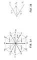
- FIGS 2A and 2B are vector diagrams illustrating control vectors for paralleled invertor 10.
- SVPWM space vector pulse-width modulation
- V ref is generated based upon the desired three-phase output (V A , V B and V C ) of paralleled inverter 10.
- V ref may be generated using any desired method, such as converting a desired three-phase output (V A , V B , and V C ) into a two-dimensional DQ or ⁇ reference frame using a Park and/or Clarke transformation.
- the resultant V ref control vector will fall into one of the six sectors shown in FIG. 2A .
- the transformation will also provide the angle ⁇ of the position of V ref .
- the six unit vectors (0,0,1; 0,1,0; 0,1,1; 1,0,0; 1,0,1; and 1,1,0) as shown in FIG. 2A are utilized to control the inverter.
- switches S 1b , S 1c , and S 1f would be enabled to provide -V DC /2 to the V A1 output, V DC /2 to the V B1 output, and -V DC /2 to the V C1 output.
- Each of inverters 12a and 12b may be controlled utilizing these six single two-stage inverter unit vectors.
- paralleled inverter 10 For paralleled inverter 10, six new unit vectors (1,0,2; 2,0,1; 2,1,0; 1,2,0; 0,2,1; and 0,1,2), as shown in FIG. 2A , may be utilized as combinations of adjacent single inverter unit vectors.
- paralleled inverter unit vector 1,0,2 is formed through combination of single inverter unit vectors 0,0,1 and 1,0,1
- paralleled inverter unit vector 2,0,1 is formed through combination of single inverter unit vectors 1,0,1 and 1,0,0.
- inverter 12a may be controlled using single inverter unit vector 1,0,1
- inverter 12b may be controlled using single inverter unit vector 1,0,0.
- inverter 12a may be controlled using single inverter unit vector 1,0,0
- inverter 12b may be controlled using single inverter unit vector 1,0,1.
- parallel inverter 10 When controlled using the six new unit vectors (1,0,2; 2,0,1; 2,1,0; 1,2,0; 0,2,1; and 0,1,2), parallel inverter 10 produces zero or negligible CM voltage on outputs V A -V C .
- This negligible CM voltage may be, for example, less than one percent of V DC .
- switches S 1b , S 1d , S 1e , S 2a , S 2d , and S 2e would be enabled providing zero volts on V A , -V DC on V B , and +V DC on V C , which provides zero CM voltage between V A , V B , and V C .
- FIG. 2B illustrates a sample control vector V ref that is utilized to control inverters 12a and 12b to obtain a desired output (V A , V B , and V C ).
- a control vector is produced based upon a desired three-phase output (V A , V B , and V C ).
- the control vector may be generated using any method, such as a Park and/or Clarke transformation.
- the control vector will fall somewhere within the vector diagram shown in FIG. 2A .
- a sample control vector V ref is shown in Sector 1.
- vector V 1 of FIG. 2B corresponds to new unit vector 2,1,0
- vector V 2 of FIG. 2B corresponds to new vector 2,0,1.
- the angle ⁇ is the angle between new unit vector V 2 and control vector V ref .
- control vector V ref may be obtained by operating parallel inverter 10 utilizing unit vector 2,1,0 for a first time period t 1 , and operating parallel inverter 10 utilizing unit vector 2,0,1 for a second time period t 2 . Because t 1 and t 2 may not equal an entire switching period T S , another time period, t 0 , is determined for which the outputs V A , V B , and V C will all be zero. This is achieved by utilizing zero unit vectors 1,1,1 and 0,0,0, or vice versa, to control inverters 12a and 12b, respectively.
- inverters 12a and 12b may be controlled to provide the desired output indicated by control vector V ref .
- the switching period T S may be split into two half cycles. Each half cycle may include half of each of t 0 , t 1 and t 2 .
- the progression for each cycle may be t 0 /4, t 1 /2, t 2 /2, t 0 /2, t 1 /2, t 2 /2, and t 0 /4.
- inverter 12a may be controlled with single inverter unit vector 0,1,0 and inverter 12b may be controlled with single inverter unit vector 1,1,0 for the first half of period t 1 .
- inverter 12a may be controlled with single inverter unit vector 1,1,0 and inverter 12b may be controlled with single inverter unit vector 0,1,0.
- each phase of each inverter 12a and 12b only changes state twice each switching cycle (i.e. from a '0' to a '1' or from a '1' to a '0').
- the sequence progressed t 0 /4, t 1 /2, t 2 /2, t 0 /2, t 2 /2, t 1 /2, and t 0 /4 for symmetry in each half of the switching cycle (T S /2).
- each half of the switching cycle does not need to be symmetric, and the sequence may progress as shown in Tables 1-6 to achieve minimum switching events for each phase of paralleled inverter 10.
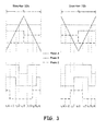
- FIG. 3 a chart illustrating control waveforms in a switching cycle (T S ) for a paralleled invertor that produces a zero CM voltage output in sector 1 (Table 1).
- the top waveform illustrates comparator waveforms and a triangle-wave carrier signal.
- the waveforms shown in FIG. 3 are for a control vector V ref in sector one as illustrated in FIG. 2A . Because the two half cycles of T S are not symmetrical, some of the comparator signals include a step up or down at the half cycle.
- the comparator signals may be utilized to generate the control signals for each of inverters 12a and 12b.
- control signals 3 are compared to the triangle-wave carrier signal to generate a control signal for each phase.
- the control signals are illustrated in the bottom waveform of FIG. 3 and correspond to the values shown in Table 1.
- comparator signals will be generated that will be utilized to generate the control signals indicated in a respective Table 2-6.
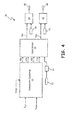
- FIG. 4 is a block diagram illustrating a controller 20 for paralleled inverter 10.
- Control system 20 includes comparator calculator 22, pulse divider 24, and PWM calculators 26 and 28.
- Comparator calculator 22 provides outputs 30a-30d to pulse divider 24.
- Pulse divider 24 receives input from triangle-wave carrier input 32 through derivative module 34.
- Pulse divider 24 provides output 36a to PWM calculator 26 and provides output 36b to PWM calculator 28.
- PWM calculator 26 receives input from triangle-wave carrier input 38 and provides PWM output 40.
- PWM calculator 28 receives input from triangle-wave carrier input 42 and provides PWM output 44.
- Control system 20 may be implemented as any electronic system capable of providing control signals for inverters 12a and 12b.
- Control system 20 may be, for example, implemented in software and run on a microprocessor, may be implemented as discrete electronic components, or as any other electronic system.
- Comparator 22 receives a control vector V ref and angle ⁇ from, for example, a separate controller, or the same controller that implements control system 20. Comparator 22 determines values for t 0 , t 1 and t 2 using, for example, equation (2). Following determination of t 0 , t 1 , and t 2 , based upon the sector in which V ref falls, comparator 22 produces the comparator signals illustrated in FIG. 3 , based upon the respective tables 1-6.
- Comparator 22 generates a first set of comparator values 30a for inverter 12a, a second set of comparator values 30b for inverter 12a, a first set of comparator values 30c for inverter 12b, and a second set of comparator values 30d for inverter 12b.
- the first set for each of inverters 12a and 12b are comparator values for a first half cycle of a switching period T S
- the second set for each of inverters 12a and 12b are comparator values for a second half cycle of the switching period T S .
- Pulse divider 24 receives the four sets of comparator values 30a-30d and also receives an input from derivative module 34. The input is indicative of a change in triangle carrier wave input 32. In this way, pulse divider 24 is able to determine the present half cycle of T S . Based upon the present half cycle of TS, pulse divider 24 provides the respective comparator signals to PWM calculators 26 and 28. PWM calculator 26 compares the comparator signals with a triangle-wave carrier input signal from input 38 and PWM calculator 28 compares the comparator signals with a triangle-wave carrier input signal from input 42. This comparison is illustrated in FIG. 3 . PWM calculator 26 provides control signals (shown in FIG.
- PWM calculator 28 provides control signals (shown in FIG. 3 ) for inverter 12a on PWM output 40 based upon the comparison.
- PWM calculators 26 and 28 may be implemented as any circuit capable of comparing two values and may be implemented as electronic comparators, or in software.
- FIG. 5 is a schematic diagram illustrating coupling inductor 100 for use in coupling inductors 14 ( FIG. 1 ) at the output of paralleled invertor 10 ( FIG. 1 ).
- Inductor 100 includes core 102 and windings 104a and 104b. Coupling inductor flux path 106 and leakage inductor flux paths 108a and 108b.
- core 102 may be two 'E' cores with an air gap 110 in the central leg.
- Windings 104a and 104b are wound around opposing legs, in inversed directions. For example, a positive current through winding 104a will flow in the opposite direction of a positive current in winding 104b.
- Winding 104a may be connected to one of the phase outputs (V A1 , V B1 , V C1 ) of inverter 12a, and winding 104b may be connected to one of the phase outputs (V A2 , V B2 , V C2 ) of inverter 12b.
- the outputs of windings 104a and 104b may be connected to form primary outputs (V A , V B , V C ) provided to motor 16.
- Flux path 106 shows the coupling inductor flux, which flows through the path that does not include air gap 110.
- Flux paths 108a and 108b illustrate the leakage inductor flux, which flows through air gap 110.
- Coupling inductor flux 106 is generated by the circulating current between inverters 12a and 12b, and is utilized to limit this circulating current.
- Leakage inductor flux 108a and 108b is generated by the output current from inverters 12a and 12b, and this inductance is used to filter DM noise.
- the density of coupling inductors L 1 -L 3 ( FIG. 1 ) can be high and can perform as both a DM filter as well as a circulating current control.
- CM chokes and CM capacitors may be eliminated from the circuit, which greatly improves the power density of the system.
- CM current received by motor 16 is greatly reduced, which protects the insulation and bearings of motor 16, and may increase the life span and reliability of motor 16.
- Eliminating the CM voltage may also limit output current ripple, odd harmonics of the switching frequency, and DC capacitor ripple currents.
- Paralleled inverter 10 also provides fault-tolerant control in that the system may still function upon failure of one of inverters 12a or 12b.
- a power conversion system includes a paralleled inverter and a plurality of coupling inductors.
- the paralleled inverter is configured to convert a direct current input into an alternating current output and includes a first inverter having a first plurality of phase outputs and a second inverter having a second plurality of phase outputs.
- the plurality of coupling inductors connect one of the first plurality of phase outputs with one of the second phase outputs to filter differential-mode electromagnetic interference and circulation current.
- the plurality of coupling inductors includes a first coupling inductor connected to a first output of the first plurality of phase outputs and a first output of the second phase outputs, the first coupling inductor providing a first primary output, a second coupling inductor connected to a second output of the first plurality of phase outputs and a second output of the second phase outputs, the second coupling inductor providing a second primary output, and a third coupling inductor connected to a third output of the first plurality of phase outputs and a third output of the second phase outputs, the third coupling inductor providing a third primary output.
- a further embodiment of any of the foregoing systems further including a first capacitor connected between the first primary output and a midpoint, a second capacitor connected between the second primary output and the midpoint, and a third capacitor connected between the third primary output and the midpoint, wherein the first capacitor, the second capacitor, and the third capacitor filter differential-mode noise on the first primary output, the second primary output, and the third primary output.
- each of the plurality of coupling inductors includes a core having a first leg, an opposing second leg, and a central air gap, a first coil wound around the first leg that receives a first current, and a second coil wound around the second leg that receives a second current, wherein a flux direction generated by the second current is received in an opposite direction of a flux direction generated by the first current.
- each of the plurality of coupling inductors comprises a pair of 'E' cores.
- each of the plurality of coupling inductors utilizes a coupling inductor flux generated in the core by the first and second currents to limit a circulation current in the paralleled inverter.
- each of the plurality of coupling inductors utilizes a leakage inductor flux generated in the core by the first and second currents to filter differential-mode noise in the paralleled inverter.
- a further embodiment of any of the foregoing systems wherein the first current is received from one of the first plurality of phase outputs and the second current is received from one of the second plurality of phase outputs.
- a further embodiment of any of the foregoing systems further comprising a controller that controls the paralleled converter to produce negligible common-mode voltage.
- a method of filtering differential-mode noise from a paralleled inverter including providing a first plurality of outputs from a first inverter of the paralleled inverter to a plurality of coupling inductors, providing a second plurality of outputs from a second inverter of the paralleled inverter to the plurality of coupling inductors, and filtering, using the plurality of coupling inductors, the differential-mode noise from the paralleled inverter.
- a further embodiment of the foregoing method further including controlling, using a controller, the paralleled inverter to generate negligible common-mode voltage.
- a further embodiment of any of the foregoing methods further including providing power on a plurality of primary outputs from the plurality of coupling inductors to drive an alternating current load.
- a further embodiment of any of the foregoing methods further including filtering, using a capacitor circuit, the differential-mode noise on the plurality of primary outputs.
Landscapes
- Engineering & Computer Science (AREA)
- Power Engineering (AREA)
- Physics & Mathematics (AREA)
- Electromagnetism (AREA)
- Inverter Devices (AREA)
Abstract
A power conversion system includes a paralleled inverter (10) and a plurality of coupling inductors (14). The paralleled inverter (10) is configured to convert a direct current input into an alternating current output and includes a first inverter (12a) having a first plurality of phase outputs and a second inverter (12b) having a second plurality of phase outputs, which may achieve negligible common-mode output voltage. The plurality of coupling inductors (14) connect one of the first plurality of phase outputs with one of the second phase outputs to filter differential-mode electromagnetic interference and circulation current.

Description
- The present invention relates generally to power inverters, and in particular to a system and method for controlling paralleled inverters using pulse-width modulation (PWM).
- Three-phase inverters are often implemented within, for example, variable speed motor drives. Three-phase inverters are utilized, for example, to convert a direct current (DC) input into an alternating current (AC) output for a motor or other load that utilizes AC power. Prior art inverters were implemented as single stage inverters having a plurality of switches. The switches are selectively enabled and disabled to convert the DC input power into controlled AC output power.
- Electromagnetic interference, or "noise," is a common problem in electrical circuit design. Noise may originate from natural sources, such as background radiation or lightning strikes, but the more common and more problematic noise is electromagnetic noise generated by components in electrical systems, such as three-phase inverters. EMI noise can be divided into two major groups: differential-mode (DM) EMI and common-mode (CM) EMI. CM noise creates several concerns such as conduction through bearings in the motor which may reduce the reliability of the motor. In prior art systems, CM filters containing, for example, CM chokes and CM capacitors are utilized to filter the CM noise. The weight of CM filters is dependent upon the CM voltage of the inverter. Different PWM schemes for inverter control can generate different CM voltage, but CM voltage cannot be eliminated for prior art two-level inverters. It is desirable to eliminate the CM output voltage of the inverter to eliminate the need for CM filters.
- A power conversion system (claim 1) includes a paralleled inverter and a plurality of coupling inductors. The paralleled inverter is configured to convert a direct current input into an alternating current output and includes a first inverter having a first plurality of phase outputs and a second inverter having a second plurality of phase outputs. The plurality of coupling inductors connect one of the first plurality of phase outputs with one of the second phase outputs to filter differential-mode electromagnetic interference and circulation current.
-
-
FIG. 1 is a circuit diagram illustrating a paralleled inverter that includes two inverters. -
FIGS. 2A and 2B are vector diagrams illustrating control vectors for a paralleled invertor. -
FIG. 3 is a chart illustrating gate pulse generation for a switching cycle of a paralleled inverter. -
FIG. 4 is a block diagram illustrating a pulse-width modulation control system for a paralleled inverter. -
FIG. 5 is a schematic diagram illustrating a coupling inductor for use in an output of a paralleled invertor. - A power conversion system is disclosed herein that includes parallel inverters for producing zero common-mode (CM) voltage output. A controller controls the paralleled inverter using six unit vectors. Each unit vector, when utilized to control the paralleled inverter, provides negligible CM voltage at the paralleled inverter output. Because of this, no CM filter is required, reducing the overall weight and cost of the power conversion system. An output filter that includes coupling inductors is configured to filter differential-mode (DM) electromagnetic interference (EMI). The coupling inductors both constrain the circulation current from the paralleled inverter as well as filter the DM voltage.
-
FIG. 1 is a circuit diagram illustratingparalleled inverter 10 that includesinverters Inverter 12a includes switches S1a-S1f andinverter 12b includes switches S2a-S2f. The three phase outputs frominverters coupling inductors 14 that include inductors L1-L3. Capacitors C1-C3 are connected between each phase output fromcoupling inductors 14 and a common point. The three phase outputs fromcoupling inductors 14 are provided to, for example, three-phase motor 16. Although illustrated as providing power to three-phase motor 16, paralleledinverter 10 may be utilized in any power conversion system to provide power for any AC load. -
Inverters parallel inverter 10 from any DC source such as, for example, an active rectifier.Inverters phase motor 16, constrains circulation current, and filters DM noise. Circulation currents are currents that flow frominverter 12a intoinverter 12b or vice versa, for example, a circulating current may flow from output VA1 into output VA2. The same operation is performed for the other outputs VB and VC. The three outputs VA, VB, and VC are provided tomotor 16. - With continued reference to
FIG. 1 ,FIGS 2A and 2B are vector diagrams illustrating control vectors forparalleled invertor 10. In space vector pulse-width modulation (SVPWM) control, a two-dimensional control vector is utilized to control the output voltage ofparalleled inverter 10. The control vector (Vref) is generated based upon the desired three-phase output (VA, VB and VC) ofparalleled inverter 10. Vref may be generated using any desired method, such as converting a desired three-phase output (VA, VB, and VC) into a two-dimensional DQ or αβ reference frame using a Park and/or Clarke transformation. The resultant Vref control vector will fall into one of the six sectors shown inFIG. 2A . The transformation will also provide the angle θ of the position of Vref. - In single two-stage inverters, the six unit vectors (0,0,1; 0,1,0; 0,1,1; 1,0,0; 1,0,1; and 1,1,0) as shown in
FIG. 2A are utilized to control the inverter. For example, if the 0,1,0 unit vector is applied to inverter 12a, switches S1b, S1c, and S1f would be enabled to provide -VDC/2 to the VA1 output, VDC/2 to the VB1 output, and -VDC/2 to the VC1 output. Each ofinverters - For
paralleled inverter 10, six new unit vectors (1,0,2; 2,0,1; 2,1,0; 1,2,0; 0,2,1; and 0,1,2), as shown inFIG. 2A , may be utilized as combinations of adjacent single inverter unit vectors. For example, paralleledinverter unit vector inverter unit vectors inverter unit vector inverter unit vectors unit vector inverter 12a may be controlled using singleinverter unit vector inverter 12b may be controlled using singleinverter unit vector 1,0,0. Additionally,inverter 12a may be controlled using singleinverter unit vector 1,0,0, andinverter 12b may be controlled using singleinverter unit vector - When controlled using the six new unit vectors (1,0,2; 2,0,1; 2,1,0; 1,2,0; 0,2,1; and 0,1,2),
parallel inverter 10 produces zero or negligible CM voltage on outputs VA-VC. This negligible CM voltage may be, for example, less than one percent of VDC. The following equation is used to calculate the CM voltage produced on outputs VA-VC:
- As seen in equation (1), with a single stage inverter, where each phase produces an output of either +VDC/2 or -VDC/2, there will be a nonzero CM voltage output due to the odd number of outputs. With
parallel inverter 10 that includes six outputs, it is possible to eliminate the CM output due to the even number of outputs. The six new unit vectors always provide an output such that VCM is equal to zero. For example, if paralleledinverter 10 is controlled usingunit vector inverter 12a may be controlled with singleinverter unit vector 0,0,1, andinverter 12b may be controlled with singleinverter unit vector -
FIG. 2B illustrates a sample control vector Vref that is utilized to controlinverters FIG. 2A . InFIGS. 2A and 2B , a sample control vector Vref is shown inSector 1. For the sample control vector Vref shown inFIG. 2A , vector V1 ofFIG. 2B corresponds tonew unit vector FIG. 2B corresponds tonew vector - As shown in
FIG. 2A , control vector Vref may be obtained by operatingparallel inverter 10 utilizingunit vector parallel inverter 10 utilizingunit vector unit vectors inverters 
- Following determination of t0, t1, and t2,
inverters inverter 10 is controlled usingunit vector inverter 12a may be controlled with singleinverter unit vector 0,1,0 andinverter 12b may be controlled with singleinverter unit vector inverter 12a may be controlled with singleinverter unit vector inverter 12b may be controlled with singleinverter unit vector 0,1,0. This provides balance for each switching cycle TS, which balances the circulating current through paralleledinverter 10 which may then be easily limited by couplinginductors 14. - Based upon the sector in which Vref is located, the following tables may be utilized to determine the desired control of inverters 12a and 12b for a given switching cycle TS.
Table 1 Sector One Inverter 12a Inverter 12b t0/4 1,1,1 0,0,0 t1/2 1,1,0 1,0,0 t2/2 1,0,0 1,0,1 t0/2 0,0,0 1,1,1 t1/2 1,0,0 1,1,0 t2/2 1,0,1 1,0,0 t0/4 1,1,1 0,0,0 Table 2 Sector Two Inverter 12a Inverter 12b t0/4 1,1,1 0,0,0 t1/2 1,1,0 0,1,0 t2/2 1,0,0 1,1,0 t0/2 0,0,0 1,1,1 t1/2 0,1,0 1,1,0 t2/2 1,1,0 1,0,0 t0/4 1,1,1 0,0,0 Table 3 Sector Three Inverter 12a Inverter 12b t0/4 1,1,1 0,0,0 t1/2 0,1,1 0,1,0 t2/2 0,1,0 1,1,0 t0/2 0,0,0 1,1,1 t1/2 0,1,0 0,1,1 t2/2 1,1,0 0,1,0 t0/4 1,1,1 0,0,0 Table 4 Sector Four Inverter 12a Inverter 12b t0/4 1,1,1 0,0,0 t1/2 0,1,1 0,0,1 t2/2 0,1,0 0,1,1 t0/2 0,0,0 1,1,1 t1/2 0,0,1 0,1,1 t2/2 0,1,1 0,1,0 t0/4 1,1,1 0,0,0 Table 5 Sector Five Inverter 12a Inverter 12b t0/4 1,1,1 0,0,0 t1/2 1,0,1 0,0,1 t2/2 0,0,1 0,1,1 t0/2 0,0,0 1,1,1 t1/2 0,0,1 1,0,1 t2/2 0,1,1 0,0,1 t0/4 1,1,1 0,0,0 Table 6 Sector Six Inverter 12a Inverter 12b t0/4 1,1,1 0,0,0 t1/2 1,0,1 1,0,0 t2/2 0,0,1 1,0,1 t0/2 0,0,0 1,1,1 t1/2 1,0,0 1,0,1 t2/2 1,0,1 0,0,1 t0/4 1,1,1 0,0,0 - As shown in Tables 1-6, each phase of each
inverter inverter 10 producing no CM output voltage, each half of the switching cycle does not need to be symmetric, and the sequence may progress as shown in Tables 1-6 to achieve minimum switching events for each phase of paralleledinverter 10. - With continued reference to
FIG. 1 andFIGS. 2A and2B ,FIG. 3 a chart illustrating control waveforms in a switching cycle (TS) for a paralleled invertor that produces a zero CM voltage output in sector 1 (Table 1). The top waveform illustrates comparator waveforms and a triangle-wave carrier signal. The waveforms shown inFIG. 3 are for a control vector Vref in sector one as illustrated inFIG. 2A . Because the two half cycles of TS are not symmetrical, some of the comparator signals include a step up or down at the half cycle. The comparator signals may be utilized to generate the control signals for each ofinverters FIG. 3 are compared to the triangle-wave carrier signal to generate a control signal for each phase. The control signals are illustrated in the bottom waveform ofFIG. 3 and correspond to the values shown in Table 1. For control vectors that fall in the other sectors, comparator signals will be generated that will be utilized to generate the control signals indicated in a respective Table 2-6. - With continued reference to
FIGS. 1-3 ,FIG. 4 is a block diagram illustrating acontroller 20 for paralleledinverter 10.Control system 20 includescomparator calculator 22,pulse divider 24, andPWM calculators Comparator calculator 22 providesoutputs 30a-30d topulse divider 24.Pulse divider 24 receives input from triangle-wave carrier input 32 throughderivative module 34.Pulse divider 24 providesoutput 36a toPWM calculator 26 and providesoutput 36b toPWM calculator 28.PWM calculator 26 receives input from triangle-wave carrier input 38 and providesPWM output 40.PWM calculator 28 receives input from triangle-wave carrier input 42 and providesPWM output 44.Control system 20 may be implemented as any electronic system capable of providing control signals forinverters Control system 20 may be, for example, implemented in software and run on a microprocessor, may be implemented as discrete electronic components, or as any other electronic system. -
Comparator 22 receives a control vector Vref and angle θ from, for example, a separate controller, or the same controller that implementscontrol system 20.Comparator 22 determines values for t0, t1 and t2 using, for example, equation (2). Following determination of t0, t1, and t2, based upon the sector in which Vref falls,comparator 22 produces the comparator signals illustrated inFIG. 3 , based upon the respective tables 1-6.Comparator 22 generates a first set ofcomparator values 30a forinverter 12a, a second set ofcomparator values 30b forinverter 12a, a first set ofcomparator values 30c forinverter 12b, and a second set ofcomparator values 30d forinverter 12b. The first set for each ofinverters inverters -
Pulse divider 24 receives the four sets ofcomparator values 30a-30d and also receives an input fromderivative module 34. The input is indicative of a change in trianglecarrier wave input 32. In this way,pulse divider 24 is able to determine the present half cycle of TS. Based upon the present half cycle of TS,pulse divider 24 provides the respective comparator signals toPWM calculators PWM calculator 26 compares the comparator signals with a triangle-wave carrier input signal frominput 38 andPWM calculator 28 compares the comparator signals with a triangle-wave carrier input signal frominput 42. This comparison is illustrated inFIG. 3 .PWM calculator 26 provides control signals (shown inFIG. 3 ) forinverter 12a onPWM output 40 based upon the comparison, andPWM calculator 28 provides control signals (shown inFIG. 3 ) forinverter 12b onPWM output 44 based upon the comparison.PWM calculators - With continued reference to
FIGS. 1-4 ,FIG. 5 is a schematic diagram illustratingcoupling inductor 100 for use in coupling inductors 14 (FIG. 1 ) at the output of paralleled invertor 10 (FIG. 1 ).Inductor 100 includescore 102 andwindings inductor flux path 106 and leakageinductor flux paths FIG. 5 ,core 102 may be two 'E' cores with anair gap 110 in the central leg. -
Windings inverter 12a, and winding 104b may be connected to one of the phase outputs (VA2, VB2, VC2) ofinverter 12b. The outputs ofwindings motor 16. -
Flux path 106 shows the coupling inductor flux, which flows through the path that does not includeair gap 110.Flux paths air gap 110. Couplinginductor flux 106 is generated by the circulating current betweeninverters Leakage inductor flux inverters coupling inductor 100, the density of coupling inductors L1-L3 (FIG. 1 ) can be high and can perform as both a DM filter as well as a circulating current control. - By utilizing paralleled
inverter 10 withcoupling inductors 14 and capacitors C1-C3, a power conversion system may be implemented that produces negligible CM voltage. Because of this, prior art CM chokes and CM capacitors may be eliminated from the circuit, which greatly improves the power density of the system. By eliminating CM output of paralleledinverter 10, the CM current received bymotor 16 is greatly reduced, which protects the insulation and bearings ofmotor 16, and may increase the life span and reliability ofmotor 16. Eliminating the CM voltage may also limit output current ripple, odd harmonics of the switching frequency, and DC capacitor ripple currents.Paralleled inverter 10 also provides fault-tolerant control in that the system may still function upon failure of one ofinverters - The following are non-exclusive descriptions of possible embodiments of the present invention.
- A power conversion system includes a paralleled inverter and a plurality of coupling inductors. The paralleled inverter is configured to convert a direct current input into an alternating current output and includes a first inverter having a first plurality of phase outputs and a second inverter having a second plurality of phase outputs. The plurality of coupling inductors connect one of the first plurality of phase outputs with one of the second phase outputs to filter differential-mode electromagnetic interference and circulation current.
- A further embodiment of the foregoing system, wherein the plurality of coupling inductors includes a first coupling inductor connected to a first output of the first plurality of phase outputs and a first output of the second phase outputs, the first coupling inductor providing a first primary output, a second coupling inductor connected to a second output of the first plurality of phase outputs and a second output of the second phase outputs, the second coupling inductor providing a second primary output, and a third coupling inductor connected to a third output of the first plurality of phase outputs and a third output of the second phase outputs, the third coupling inductor providing a third primary output.
- A further embodiment of any of the foregoing systems, further including a first capacitor connected between the first primary output and a midpoint, a second capacitor connected between the second primary output and the midpoint, and a third capacitor connected between the third primary output and the midpoint, wherein the first capacitor, the second capacitor, and the third capacitor filter differential-mode noise on the first primary output, the second primary output, and the third primary output.
- A further embodiment of any of the foregoing systems, wherein the alternating current output is provided to an alternating current load.
- A further embodiment of any of the foregoing systems, wherein each of the plurality of coupling inductors includes a core having a first leg, an opposing second leg, and a central air gap, a first coil wound around the first leg that receives a first current, and a second coil wound around the second leg that receives a second current, wherein a flux direction generated by the second current is received in an opposite direction of a flux direction generated by the first current.
- A further embodiment of any of the foregoing systems, wherein the core of each of the plurality of coupling inductors comprises a pair of 'E' cores.
- A further embodiment of any of the foregoing systems, wherein each of the plurality of coupling inductors utilizes a coupling inductor flux generated in the core by the first and second currents to limit a circulation current in the paralleled inverter.
- A further embodiment of any of the foregoing systems, wherein each of the plurality of coupling inductors utilizes a leakage inductor flux generated in the core by the first and second currents to filter differential-mode noise in the paralleled inverter.
- A further embodiment of any of the foregoing systems, wherein the first current is received from one of the first plurality of phase outputs and the second current is received from one of the second plurality of phase outputs.
- A further embodiment of any of the foregoing systems, further comprising a controller that controls the paralleled converter to produce negligible common-mode voltage.
- A method of filtering differential-mode noise from a paralleled inverter, the method including providing a first plurality of outputs from a first inverter of the paralleled inverter to a plurality of coupling inductors, providing a second plurality of outputs from a second inverter of the paralleled inverter to the plurality of coupling inductors, and filtering, using the plurality of coupling inductors, the differential-mode noise from the paralleled inverter.
- A further embodiment of the foregoing method, further including controlling, using a controller, the paralleled inverter to generate negligible common-mode voltage.
- A further embodiment of any of the foregoing methods, further including providing power on a plurality of primary outputs from the plurality of coupling inductors to drive an alternating current load.
- A further embodiment of any of the foregoing methods, further including filtering, using a capacitor circuit, the differential-mode noise on the plurality of primary outputs.
- While the invention has been described with reference to an exemplary embodiment(s), it will be understood by those skilled in the art that various changes may be made without departing from the scope of the invention. In addition, many modifications may be made to adapt a particular situation or material to the teachings of the invention without departing from the essential scope thereof. Therefore, it is intended that the invention not be limited to the particular embodiment(s) disclosed, but that the invention will include all embodiments falling within the scope of the appended claims.
Claims (14)
- A power conversion system comprising:a paralleled inverter (10) configured to convert a direct current input into an alternating current output, wherein the paralleled inverter (10) includes a first inverter (12a) having a first plurality of phase outputs and a second inverter (12b) having a second plurality of phase outputs; anda plurality of coupling inductors (14), wherein each of the plurality of coupling inductors connects one of the first plurality of phase outputs with one of the second phase outputs to filter differential-mode electromagnetic interference and circulation current.
- The power conversion system of claim 1, wherein the plurality of coupling inductors (14) comprises:a first coupling inductor (L1) connected to a first output of the first plurality of phase outputs and a first output of the second phase outputs, the first coupling inductor providing a first primary output;a second coupling inductor (L2) connected to a second output of the first plurality of phase outputs and a second output of the second phase outputs, the second coupling inductor providing a second primary output; anda third coupling inductor (L3) connected to a third output of the first plurality of phase outputs and a third output of the second phase outputs, the third coupling inductor providing a third primary output.
- The power conversion system of claim 2, further comprising:a first capacitor (C1) connected between the first primary output and a midpoint;a second capacitor (C2) connected between the second primary output and the midpoint; anda third capacitor (C3) connected between the third primary output and the midpoint, wherein the first capacitor, the second capacitor, and the third capacitor filter differential-mode noise on the first primary output, the second primary output, and the third primary output.
- The power conversion system of claim 2, wherein the alternating current output is provided to an alternating current load.
- The power conversion system of claim 1, wherein each of the plurality of coupling inductors (14) comprises:a core (102) having a first leg, an opposing second leg, and a central air gap (110);a first coil (104a) wound around the first leg that receives a first current; anda second coil (104b) wound around the second leg that receives a second current, wherein a flux direction generated by the second current is received in an opposite direction of a flux direction generated by the first current.
- The power conversion system of claim 5, wherein the core of each of the plurality of coupling inductors (14) comprises a pair of 'E' cores.
- The power conversion system of claim 5, wherein each of the plurality of coupling inductors (14) utilizes a coupling inductor flux generated in the core by the first and second currents to limit a circulation current in the paralleled inverter.
- The power conversion system of claim 5, wherein each of the plurality of coupling inductors (14) utilizes a leakage inductor flux generated in the core by the first and second currents to filter differential-mode noise in the paralleled inverter.
- The power conversion system of claim 5, wherein the first current is received from one of the first plurality of phase outputs and the second current is received from one of the second plurality of phase outputs.
- The power conversion system of claim 1, further comprising a controller that controls the paralleled converter to produce negligible common-mode voltage.
- A method of filtering differential-mode noise from a paralleled inverter (10), the method comprising:providing a first plurality of outputs from a first inverter of the paralleled inverter to a plurality of coupling inductors (14);providing a second plurality of outputs from a second inverter of the paralleled inverter to the plurality of coupling inductors (14); andfiltering, using the plurality of coupling inductors (14), the differential-mode noise from the paralleled inverter.
- The method of claim 11, further comprising controlling, using a controller, the paralleled inverter to generate negligible common-mode voltage.
- The method of claim 11, further comprising providing power on a plurality of primary outputs from the plurality of coupling inductors to drive an alternating current load.
- The method of claim 13, further comprising filtering, using a capacitor circuit, the differential-mode noise on the plurality of primary outputs.
Applications Claiming Priority (1)
| Application Number | Priority Date | Filing Date | Title |
|---|---|---|---|
| US14/291,908 US20150349626A1 (en) | 2014-05-30 | 2014-05-30 | Output filter for paralleled inverter |
Publications (1)
| Publication Number | Publication Date |
|---|---|
| EP2950434A1 true EP2950434A1 (en) | 2015-12-02 |
Family
ID=53284018
Family Applications (1)
| Application Number | Title | Priority Date | Filing Date |
|---|---|---|---|
| EP15169118.5A Withdrawn EP2950434A1 (en) | 2014-05-30 | 2015-05-26 | Output filter with interphase reactor for paralleled inverters |
Country Status (2)
| Country | Link |
|---|---|
| US (1) | US20150349626A1 (en) |
| EP (1) | EP2950434A1 (en) |
Cited By (13)
| Publication number | Priority date | Publication date | Assignee | Title |
|---|---|---|---|---|
| CN106208750A (en) * | 2015-06-01 | 2016-12-07 | 奥的斯电梯公司 | There is the active front-end rectifier of parallel connection of negligible common mode |
| CN106655648A (en) * | 2016-11-30 | 2017-05-10 | 华中科技大学 | Modular motor system and driving control method therefor |
| EP3355467A1 (en) * | 2017-01-30 | 2018-08-01 | Otis Elevator Company | Parallel interleaved 2-level or 3-level regenerative drives |
| CN105978378B (en) * | 2016-06-01 | 2018-08-28 | 西安交通大学 | A kind of circulation of inverter parallel connection detects and controls method |
| CN108621862A (en) * | 2017-03-15 | 2018-10-09 | 华为技术有限公司 | Electric driving control system, electric vehicle and electric drive control method |
| TWI681611B (en) * | 2018-05-14 | 2020-01-01 | 國立勤益科技大學 | Tolerant control system of three-level t-type inverter and tolerant control method thereof |
| CN110829870A (en) * | 2019-10-28 | 2020-02-21 | 杭州电子科技大学 | Control method of modular multilevel converter in low-frequency operation state |
| US10833603B2 (en) | 2017-01-30 | 2020-11-10 | Carrier Corporation | Method of controlling paralleled passive front-end rectifiers with and without inter-leaving |
| CN111934573A (en) * | 2020-07-16 | 2020-11-13 | 苏州伟创电气科技股份有限公司 | Current sharing control method and system |
| US10944335B2 (en) | 2017-01-30 | 2021-03-09 | Carrier Corporation | Paralleled passive front-end rectifiers with and without interleaving |
| KR20210083649A (en) * | 2019-12-27 | 2021-07-07 | 한국항공우주연구원 | Dc-dc converting apparatus using coupling among output inductors |
| AT523577A1 (en) * | 2020-03-05 | 2021-09-15 | Avl List Gmbh | Machine converter and method for operating a machine converter |
| DE102022103770A1 (en) | 2022-02-17 | 2023-08-17 | Dr. Ing. H.C. F. Porsche Aktiengesellschaft | Traction drive inverter arrangement |
Families Citing this family (11)
| Publication number | Priority date | Publication date | Assignee | Title |
|---|---|---|---|---|
| US9985566B2 (en) * | 2015-05-29 | 2018-05-29 | Otis Elevator Company | Dual three-phase electrical machine and drive with negligible common-mode noise |
| CN108604862B (en) * | 2016-02-24 | 2021-02-09 | 本田技研工业株式会社 | Power supply device, apparatus, and control method |
| EP3542455B1 (en) * | 2016-11-16 | 2025-08-13 | Schneider Electric Solar Inverters USA, Inc. | Interleaved parallel inverters with integrated filter inductor and interphase transformer |
| JP6904201B2 (en) * | 2017-09-27 | 2021-07-14 | セイコーエプソン株式会社 | Robot control devices, robots, and robot systems |
| JP7157412B2 (en) * | 2018-04-27 | 2022-10-20 | 国立大学法人長岡技術科学大学 | three phase inverter |
| CN110176866B (en) * | 2019-04-11 | 2020-09-18 | 华中科技大学 | 2N inverter parallel system and control method thereof |
| US11271512B2 (en) * | 2019-06-07 | 2022-03-08 | U-Mhi Platech Co., Ltd. | Motor driving device |
| WO2021170239A1 (en) * | 2020-02-27 | 2021-09-02 | Abb Schweiz Ag | Parallel npc 3-level inverter without midpoint connection of the dc-links |
| AT523576A1 (en) * | 2020-03-05 | 2021-09-15 | Avl List Gmbh | Converter arrangement |
| US11942887B2 (en) * | 2021-12-02 | 2024-03-26 | Dana Tm4 Italia S.R.L. | Dual segmented motor drive |
| EP4340214B1 (en) * | 2022-09-16 | 2025-12-17 | Hamilton Sundstrand Corporation | Multi-three-phase drive system |
Citations (1)
| Publication number | Priority date | Publication date | Assignee | Title |
|---|---|---|---|---|
| US20110299311A1 (en) * | 2010-12-17 | 2011-12-08 | Huibin Zhu | Power Generation System, Power Converter System, And Methods Of Converting Power |
Family Cites Families (7)
| Publication number | Priority date | Publication date | Assignee | Title |
|---|---|---|---|---|
| US8963521B2 (en) * | 2007-06-08 | 2015-02-24 | Intersil Americas LLC | Power supply with a magnetically uncoupled phase and an odd number of magnetically coupled phases, and control for a power supply with magnetically coupled and magnetically uncoupled phases |
| EP2237403A1 (en) * | 2009-03-30 | 2010-10-06 | SMA Solar Technology AG | Inverter with two asymmetric bridges and a free-wheeling path decoupling the DC input from the AC output |
| JP5652659B2 (en) * | 2011-03-30 | 2015-01-14 | アイシン・エィ・ダブリュ株式会社 | Electric motor control device |
| JP5477408B2 (en) * | 2012-03-02 | 2014-04-23 | 株式会社安川電機 | Power converter |
| JP5590076B2 (en) * | 2012-07-04 | 2014-09-17 | 株式会社デンソー | Control device for multi-phase rotating machine |
| EP2770624B1 (en) * | 2013-02-22 | 2017-02-22 | ABB Research Ltd. | Method and apparatus for producing three-phase current |
| US20150145462A1 (en) * | 2013-11-25 | 2015-05-28 | Rockwell Automation Technologies, Inc. | Method and apparatus for current auto balancing for parallel converter systems |
-
2014
- 2014-05-30 US US14/291,908 patent/US20150349626A1/en not_active Abandoned
-
2015
- 2015-05-26 EP EP15169118.5A patent/EP2950434A1/en not_active Withdrawn
Patent Citations (1)
| Publication number | Priority date | Publication date | Assignee | Title |
|---|---|---|---|---|
| US20110299311A1 (en) * | 2010-12-17 | 2011-12-08 | Huibin Zhu | Power Generation System, Power Converter System, And Methods Of Converting Power |
Non-Patent Citations (3)
| Title |
|---|
| BOILLAT D O ET AL: "Modeling and experimental analysis of a Coupling Inductor employed in a high performance AC power source", RENEWABLE ENERGY RESEARCH AND APPLICATIONS (ICRERA), 2012 INTERNATIONAL CONFERENCE ON, IEEE, 11 November 2012 (2012-11-11), pages 1 - 18, XP032440255, ISBN: 978-1-4673-2328-4, DOI: 10.1109/ICRERA.2012.6477401 * |
| DI ZHANG ET AL: "Total Flux Minimization Control for Integrated Inter-Phase Inductors in Paralleled, Interleaved Three-Phase Two-Level Voltage-Source Converters With Discontinuous Space-Vector Modulation", IEEE TRANSACTIONS ON POWER ELECTRONICS, INSTITUTE OF ELECTRICAL AND ELECTRONICS ENGINEERS, USA, vol. 27, no. 4, 1 April 2012 (2012-04-01), pages 1679 - 1688, XP011422919, ISSN: 0885-8993, DOI: 10.1109/TPEL.2011.2169281 * |
| ZHIHONG YE ET AL: "Paralleling non-isolated multi-phase PWM converters", INDUSTRY APPLICATIONS CONFERENCE, 2000. CONFERENCE RECORD OF THE 2000 IEEE 8-12 OCTOBER 2000, PISCATAWAY, NJ, USA,IEEE, vol. 4, 8 October 2000 (2000-10-08), pages 2433 - 2439, XP010522596, ISBN: 978-0-7803-6401-1 * |
Cited By (17)
| Publication number | Priority date | Publication date | Assignee | Title |
|---|---|---|---|---|
| EP3104517A3 (en) * | 2015-06-01 | 2016-12-28 | Otis Elevator Company | Paralleled active front-end rectifiers with negligible common-mode |
| CN106208750A (en) * | 2015-06-01 | 2016-12-07 | 奥的斯电梯公司 | There is the active front-end rectifier of parallel connection of negligible common mode |
| CN105978378B (en) * | 2016-06-01 | 2018-08-28 | 西安交通大学 | A kind of circulation of inverter parallel connection detects and controls method |
| CN106655648A (en) * | 2016-11-30 | 2017-05-10 | 华中科技大学 | Modular motor system and driving control method therefor |
| US10944335B2 (en) | 2017-01-30 | 2021-03-09 | Carrier Corporation | Paralleled passive front-end rectifiers with and without interleaving |
| EP3355467A1 (en) * | 2017-01-30 | 2018-08-01 | Otis Elevator Company | Parallel interleaved 2-level or 3-level regenerative drives |
| CN108377118A (en) * | 2017-01-30 | 2018-08-07 | 奥的斯电梯公司 | The double level of paralleling and interleaving type or three levels of regenerative drivers |
| US10833603B2 (en) | 2017-01-30 | 2020-11-10 | Carrier Corporation | Method of controlling paralleled passive front-end rectifiers with and without inter-leaving |
| CN108377118B (en) * | 2017-01-30 | 2022-08-16 | 奥的斯电梯公司 | Parallel interleaved bi-level or tri-level regenerative drive |
| CN108621862A (en) * | 2017-03-15 | 2018-10-09 | 华为技术有限公司 | Electric driving control system, electric vehicle and electric drive control method |
| TWI681611B (en) * | 2018-05-14 | 2020-01-01 | 國立勤益科技大學 | Tolerant control system of three-level t-type inverter and tolerant control method thereof |
| CN110829870A (en) * | 2019-10-28 | 2020-02-21 | 杭州电子科技大学 | Control method of modular multilevel converter in low-frequency operation state |
| KR20210083649A (en) * | 2019-12-27 | 2021-07-07 | 한국항공우주연구원 | Dc-dc converting apparatus using coupling among output inductors |
| AT523577A1 (en) * | 2020-03-05 | 2021-09-15 | Avl List Gmbh | Machine converter and method for operating a machine converter |
| AT523577B1 (en) * | 2020-03-05 | 2024-06-15 | Avl List Gmbh | Machine converter and method for operating a machine converter |
| CN111934573A (en) * | 2020-07-16 | 2020-11-13 | 苏州伟创电气科技股份有限公司 | Current sharing control method and system |
| DE102022103770A1 (en) | 2022-02-17 | 2023-08-17 | Dr. Ing. H.C. F. Porsche Aktiengesellschaft | Traction drive inverter arrangement |
Also Published As
| Publication number | Publication date |
|---|---|
| US20150349626A1 (en) | 2015-12-03 |
Similar Documents
| Publication | Publication Date | Title |
|---|---|---|
| EP2950440B1 (en) | Pulse-width modulation control of paralleled inverters | |
| US20150349626A1 (en) | Output filter for paralleled inverter | |
| Jiang et al. | Common-mode voltage reduction for paralleled inverters | |
| Edpuganti et al. | New optimal pulsewidth modulation for single DC-link dual-inverter fed open-end stator winding induction motor drive | |
| Hatti et al. | A 6.6-kV transformerless motor drive using a five-level diode-clamped PWM inverter for energy savings of pumps and blowers | |
| US10773922B2 (en) | Drive and control for six-phase electrical machines with negligible common-mode voltage | |
| US20060267542A1 (en) | Pulse width modulation (PWM) rectifier with variable switching frequency | |
| EP2835902A1 (en) | Power conversion device | |
| EP3104517A2 (en) | Paralleled active front-end rectifiers with negligible common-mode | |
| US20160028341A1 (en) | Systems and methods for zero common mode voltage | |
| WO2019171568A1 (en) | Power conversion device | |
| Caris et al. | Generalized harmonic elimination method for interleaved power amplifiers | |
| US11128212B1 (en) | Current ripple reduction for a direct current source powering an alternating current load | |
| Krishnapriya et al. | Multilevel inverter fed induction motor drives | |
| Jiang et al. | Paralleled inverters with zero common-mode voltage | |
| JP6091405B2 (en) | Elevator car power supply device | |
| WO2013151542A1 (en) | Multilevel converter | |
| Xing et al. | Motor drive system EMI reduction by asymmetric interleaving | |
| Tian et al. | A space vector modulation method for common-mode voltage reduction in nested neutral point clamped inverter | |
| Singh et al. | Minimization of line current harmonics in multiple single-phase active fec fed mw railways propulsion system | |
| Cougo et al. | Impact of PWM methods and load configuration in the design of intercell transformers used in parallel three-phase inverters | |
| Salmon et al. | Eliminating common mode winding voltages for a 3-limb coupled inductor used in 3/5-level PWM voltage source inverters | |
| Hedayati et al. | A novel integrated CM inductor for parallel converters with interleaved carrier | |
| Videt et al. | PWM strategy for common-mode voltage reduction in three-phase variable-speed drives with active front end | |
| Komurcugil et al. | Passivity-based control strategy for single-phase three-level T-type PWM rectifiers |
Legal Events
| Date | Code | Title | Description |
|---|---|---|---|
| AK | Designated contracting states |
Kind code of ref document: A1 Designated state(s): AL AT BE BG CH CY CZ DE DK EE ES FI FR GB GR HR HU IE IS IT LI LT LU LV MC MK MT NL NO PL PT RO RS SE SI SK SM TR |
|
| AX | Request for extension of the european patent |
Extension state: BA ME |
|
| PUAI | Public reference made under article 153(3) epc to a published international application that has entered the european phase |
Free format text: ORIGINAL CODE: 0009012 |
|
| STAA | Information on the status of an ep patent application or granted ep patent |
Free format text: STATUS: THE APPLICATION IS DEEMED TO BE WITHDRAWN |
|
| 18D | Application deemed to be withdrawn |
Effective date: 20160603 |