EP2950202A1 - Processor and data gathering method - Google Patents
Processor and data gathering method Download PDFInfo
- Publication number
- EP2950202A1 EP2950202A1 EP15167062.7A EP15167062A EP2950202A1 EP 2950202 A1 EP2950202 A1 EP 2950202A1 EP 15167062 A EP15167062 A EP 15167062A EP 2950202 A1 EP2950202 A1 EP 2950202A1
- Authority
- EP
- European Patent Office
- Prior art keywords
- data elements
- data
- memory
- areas
- control unit
- Prior art date
- Legal status (The legal status is an assumption and is not a legal conclusion. Google has not performed a legal analysis and makes no representation as to the accuracy of the status listed.)
- Withdrawn
Links
Images





Classifications
-
- G—PHYSICS
- G06—COMPUTING OR CALCULATING; COUNTING
- G06F—ELECTRIC DIGITAL DATA PROCESSING
- G06F16/00—Information retrieval; Database structures therefor; File system structures therefor
- G06F16/20—Information retrieval; Database structures therefor; File system structures therefor of structured data, e.g. relational data
- G06F16/21—Design, administration or maintenance of databases
- G06F16/217—Database tuning
-
- G—PHYSICS
- G06—COMPUTING OR CALCULATING; COUNTING
- G06F—ELECTRIC DIGITAL DATA PROCESSING
- G06F12/00—Accessing, addressing or allocating within memory systems or architectures
- G06F12/02—Addressing or allocation; Relocation
- G06F12/08—Addressing or allocation; Relocation in hierarchically structured memory systems, e.g. virtual memory systems
- G06F12/0802—Addressing of a memory level in which the access to the desired data or data block requires associative addressing means, e.g. caches
-
- G—PHYSICS
- G06—COMPUTING OR CALCULATING; COUNTING
- G06F—ELECTRIC DIGITAL DATA PROCESSING
- G06F16/00—Information retrieval; Database structures therefor; File system structures therefor
- G06F16/90—Details of database functions independent of the retrieved data types
- G06F16/903—Querying
- G06F16/90335—Query processing
- G06F16/90339—Query processing by using parallel associative memories or content-addressable memories
-
- G—PHYSICS
- G06—COMPUTING OR CALCULATING; COUNTING
- G06F—ELECTRIC DIGITAL DATA PROCESSING
- G06F9/00—Arrangements for program control, e.g. control units
- G06F9/06—Arrangements for program control, e.g. control units using stored programs, i.e. using an internal store of processing equipment to receive or retain programs
- G06F9/30—Arrangements for executing machine instructions, e.g. instruction decode
- G06F9/30003—Arrangements for executing specific machine instructions
- G06F9/30007—Arrangements for executing specific machine instructions to perform operations on data operands
- G06F9/30032—Movement instructions, e.g. MOVE, SHIFT, ROTATE, SHUFFLE
-
- G—PHYSICS
- G06—COMPUTING OR CALCULATING; COUNTING
- G06F—ELECTRIC DIGITAL DATA PROCESSING
- G06F9/00—Arrangements for program control, e.g. control units
- G06F9/06—Arrangements for program control, e.g. control units using stored programs, i.e. using an internal store of processing equipment to receive or retain programs
- G06F9/30—Arrangements for executing machine instructions, e.g. instruction decode
- G06F9/30003—Arrangements for executing specific machine instructions
- G06F9/30007—Arrangements for executing specific machine instructions to perform operations on data operands
- G06F9/30036—Instructions to perform operations on packed data, e.g. vector, tile or matrix operations
-
- G—PHYSICS
- G06—COMPUTING OR CALCULATING; COUNTING
- G06F—ELECTRIC DIGITAL DATA PROCESSING
- G06F9/00—Arrangements for program control, e.g. control units
- G06F9/06—Arrangements for program control, e.g. control units using stored programs, i.e. using an internal store of processing equipment to receive or retain programs
- G06F9/30—Arrangements for executing machine instructions, e.g. instruction decode
- G06F9/30003—Arrangements for executing specific machine instructions
- G06F9/3004—Arrangements for executing specific machine instructions to perform operations on memory
- G06F9/30043—LOAD or STORE instructions; Clear instruction
-
- G—PHYSICS
- G06—COMPUTING OR CALCULATING; COUNTING
- G06F—ELECTRIC DIGITAL DATA PROCESSING
- G06F9/00—Arrangements for program control, e.g. control units
- G06F9/06—Arrangements for program control, e.g. control units using stored programs, i.e. using an internal store of processing equipment to receive or retain programs
- G06F9/30—Arrangements for executing machine instructions, e.g. instruction decode
- G06F9/30098—Register arrangements
- G06F9/30105—Register structure
- G06F9/30109—Register structure having multiple operands in a single register
-
- G—PHYSICS
- G06—COMPUTING OR CALCULATING; COUNTING
- G06F—ELECTRIC DIGITAL DATA PROCESSING
- G06F9/00—Arrangements for program control, e.g. control units
- G06F9/06—Arrangements for program control, e.g. control units using stored programs, i.e. using an internal store of processing equipment to receive or retain programs
- G06F9/30—Arrangements for executing machine instructions, e.g. instruction decode
- G06F9/30098—Register arrangements
- G06F9/30141—Implementation provisions of register files, e.g. ports
-
- G—PHYSICS
- G06—COMPUTING OR CALCULATING; COUNTING
- G06F—ELECTRIC DIGITAL DATA PROCESSING
- G06F2212/00—Indexing scheme relating to accessing, addressing or allocation within memory systems or architectures
- G06F2212/10—Providing a specific technical effect
- G06F2212/1041—Resource optimization
- G06F2212/1044—Space efficiency improvement
-
- G—PHYSICS
- G06—COMPUTING OR CALCULATING; COUNTING
- G06F—ELECTRIC DIGITAL DATA PROCESSING
- G06F2212/00—Indexing scheme relating to accessing, addressing or allocation within memory systems or architectures
- G06F2212/16—General purpose computing application
- G06F2212/163—Server or database system
Definitions
- processors capable of executing vector operations have been developed.
- a vector operation performs a plurality of scalar operations as one operation on vector data elements.
- Published Japanese Translation of PCT International Publication for Patent Application, No. 2014-504418 discloses a gather instruction and a scatter instruction executed before and after a vector operation is performed.
- a gather instruction is an instruction for gathering data values corresponding to a plurality of designated indices of a data array from corresponding areas of a memory. The plurality of data values gathered by the gather instruction is used as an input vector of a subsequent vector operation.
- a scatter instruction is an instruction for storing data values of vector data in areas of a memory corresponding to designated indices of a data array. The respective elements of the output vector generated by a vector operation can be used as the vector data that is subject to the scatter instruction.
- a processor loads or stores a plurality of data elements included in a plurality of data sets between a memory and a storage unit in a processor by changing the storage order of the data elements.
- a method and a system with which the processor according to the embodiment is replaced, a program for causing a computer to execute the process of the device or a portion of the device, an imaging apparatus including the device, and the like are also effective as aspects of the present invention.
- the process of loading or storing data between the memory and the storage unit in the processor can be performed efficiently.
- the data set 11 includes a plurality of data elements such as data element a 101 and data element b 102.
- data element a 101 and the data element b 102 are stored in adjacent storage areas in the memory 10.
- data set 12 includes a plurality of data elements such as data element c 103 and data element d 104.
- data element c 103 and the data element d 104 are stored in adjacent storage areas in the memory 10.
- the control unit 23 sorts the read data elements to a storage unit corresponding to the data element among the plurality of storage units 21 and 22 and writes the data elements to respective data sets. For example, the control unit 23 sorts and writes the data element a 101 and the data element b 102 read for the data set 11 to the storage units 21 and 22, respectively. Moreover, the control unit 23 sorts and writes the data element c 103 and the data element d 104 read for the data set 12 to the storage units 21 and 22, respectively.
- the control unit 23 writes the read third data element to a second area (for example, the area 203) of the first storage unit (S15). Moreover, the control unit 23 writes the read fourth data element to a second area (for example, the area 204) of the second storage unit (S16).
- the area 204 may be an area corresponding to the area 203.
- the control unit 23 may write the read third data element in an area other than the area to which data has been written at least in step S12 among the area of the first storage unit.
- the control unit 23 may write the read fourth data element to an area other than the area to which data has been written at least in step S13 among the areas of the second storage unit.
- the processor 20a includes a control unit 23a and registers rgk, rg k+1 , ..., and rg k+N-1 (k is a natural number and N is a natural number of 2 or more).
- each of the registers rg k to rg k+N-1 is divided into a plurality of ways w0, w1, ..., and wQ-1 which are areas, and the same ways of the respective registers correspond to each other.
- the processor 20a reads N words collectively from a data array array[0] and writes the respective data elements to the way w0 of the respective registers rg k to rg k+N-1 .
- Embodiment 1 when gathering a plurality of data groups stored in discontinuous areas of the memory 10, such as, for example, a group formed by the data element a 101 and the data element c 103 and a group formed by the data element b 102 and the data element d 104, the time required for a data loading process can be reduced. This is because the results of accessing continuous (adjacent) memory areas are sorted and stored in the first and second storage units in the processor, and it is therefore not necessary to perform memory accesses individually. Moreover, since the read data groups are sorted and stored to the corresponding storage units, it is not necessary to execute a process of rearranging the read data groups additionally. Thus, the process of loading data between the memory and the storage unit in the processor can be performed efficiently.
- Fig. 4 is a block diagram illustrating a configuration of a data processing device 2000 including a processor 20b according to Embodiment 2.
- the data processing device 2000 includes a memory 10 and the processor 20b.
- the memory 10 is the same as that of Fig. 1 , and redundant description thereof will be omitted.
- the processor 20b includes a storage unit 21, a storage unit 22, and a control unit 23b.
- the storage units 21 and 22 have the same configuration as those of Fig. 1 . That is, the storage unit 21 is divided into at least areas 201 and 203. Moreover, the storage unit 22 is divided into at least areas 202 and 204. It is assumed that the subsequent data elements are stored in advance in the storage units 21 and 22. That is, the data element a and the data element c are stored in the areas 201 and 203 of the storage unit 21, respectively. Moreover, the data element b and the data element d are stored in the areas 202 and 204 of the storage unit 22, respectively.
- the control unit 23b writes the respective data elements in the data set to adjacent storage areas in the memory 10. For example, the control unit 23b writes the data element a 101 and the data element b 102 to the storage areas in the memory 10, corresponding to the data element a 101 and the data element b 102 of the data set 11.
- the control unit 23b also reads the data elements stored in the areas 203 and 204 collectively, puts the data elements together to form a data set, and writes the data elements to adjacent storage areas in the memory 10 corresponding to the data set 12.
- the control unit 23b writes the first and second data elements collectively to adjacent storage areas in the memory 10 (S23). For example, as described above, in one memory access process, the control unit 23b writes the data element a and the data element b to the storage areas in the memory 10 corresponding to the data element a 101 and the data element b 102 of the data set 11, respectively.
- the control unit 23b reads a third data element (for example, the data element c) from a second area (for example, the area 203) of the first storage unit (S24). Moreover, the control unit 23b reads a fourth data element (for example, the data element d) from a second area (for example, the area 204) of the second storage unit (S25).
- the area 204 may be an area corresponding to the area 203.
- the control unit 23b may read the third data element from an area other than the area from which data has been read at least in step S21 among the areas of the first storage unit.
- the control unit 23b may read the fourth data element from an area other than the area from which data has been read at least in step S22 among the areas of the second storage unit.
- the control unit 23b writes the third and fourth data elements collectively to adjacent storage areas in the memory 10 (S26). For example, in another memory access process different from that of step S23, the control unit 23b writes the data element c and the data element d to storage areas in the memory 10 corresponding to the data element c 103 and the data element d 104 of the data set 12.
- the write destination storage areas in step S26 are different from the write destination storage areas in step S23.
- Fig. 6 is a block diagram illustrating a configuration of a parity data 2000a including a processor 20c according to Embodiment 2.
- the processor 20c is used when the configuration of the processor 20b of Fig. 4 is applied to a case in which N words are read from three or more registers and written collectively to the memory 10a and areas of read source storage units (registers) are associated as ways.
- the processor 20c reads data elements from the way w0 of the respective registers rg k to rg k+N-1 and writes N words to array[0].a to array[0].n of the memory 10a in one memory access process.
- the processor 20c reads data elements similarly for each of the ways w1 to wQ-1 and writes the data elements in the same adjacent storage areas of the data set for respective ways.
- Embodiment 2 when writing data groups stored in a plurality of storage units, such as, for example, a group formed by the data elements a and b and a group formed by the data elements c and d, collectively as one data set, the time required for a data storing process can be reduced. This is because the respective data elements read individually from different storage units are written collectively to continuous (adjacent) areas, and it is therefore not necessary to perform memory access processes individually for respective data elements. Moreover, since data elements are read from the corresponding areas in a plurality of storage units, it is not necessary to execute a process of rearranging the read data elements. Thus, the process of storing data between the memory and the storage unit in the processor can be performed efficiently.
- the control unit may preferably sort the respective data elements read from the memory to any one of the plurality of storage units according to the order of the adjacent storage areas in the memory.
- the control unit may preferably write the sorted data elements to the respective sort destination storage units. For example, when data elements are stored in a memory according to the order of definitions of the member variables of a structure, the order of definitions is associated with a sort destination storage unit. By doing so, the order of reading data from a memory can be easily associated with a sort destination storage unit, and the configuration of the processor can be simplified.
- control unit may issue the request in response to an instruction for gathering the plurality of vector data elements, designate the writing position for each data set, and write the respective sorted data elements to the designated writing positions in the respective sort destination storage units. For example, when a way is designated as the writing position, data elements can be easily written to the corresponding areas in the sort destination storage units in response to a memory access to each data set.
- the vector operation unit may execute the predetermined operation on at least two of the plurality of storage units. For example, even when a vector operation is performed on data elements stored in areas which are not necessarily adjacent in a data set, data elements which are not used for the vector operation may be read collectively and such data elements themselves may not be subject to the vector operation. By doing so, a memory access process of reading a plurality of words can be performed efficiently.
- the plurality of data sets may preferably be a structure which uses the plurality of data elements as member variables, and the plurality of storage units may preferably be associated with the member variables.
- the control unit may preferably sort and write the respective read data elements to the plurality of storage units associated with the member variables. By doing so, a vector operation can be performed efficiently on a structure defined including a plurality of data types.
- the gather instruction according to this embodiment includes the following operands, for example.
- the operation circuit 44 executes a vector operation on the plurality of vector data elements read from the vector register group 47 in response to an instruction from the instruction control circuit 43 and writes the operation results to the vector register group 47.
- the vector register group 47 includes vector registers 471, 472, ..., and 47n (n is a natural number of 2 or more).
- the vector registers 471 and the like each are a storage device which is divided into areas of ways w0 to wQ-1 so as to store data elements in respective areas. That is, the vector registers 471 and the like are register files capable of storing k words per entry. However, it is assumed that the vector registers 471 and the like cannot update data in respective way units but in respective register units (that is, updates Q data elements collectively) in order to allow the operation circuit 44 to execute the vector operation at a high speed.
- vector register 471 and the buffer 461 are connected (that is, the two are associated with each other) and a set of stored data elements can be migrated between them.
- vector register 472 and the buffer 462 are connected (that is, the two are associated with each other) and a set of stored data elements can be migrated between them.
- the memory access control circuit 45 is a circuit that controls a memory access process from the processor 40 to the memory 30.
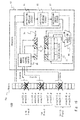
- the memory access control circuit 45 includes a request issuing unit 450, switching units 451 and 452, and a data sorting unit 453.
- the request issuing unit 450 Upon receiving a memory read request signal SIG0 from the instruction control circuit 43, the request issuing unit 450 issues a memory access (read) request to the memory 30, including a designated starting memory address A and a designated number of words N included in the signal SIG0. After that, each time receiving a response to the request, the request issuing unit 450 issues a request by adding the size C to the memory address A.
- the request aims to read a set of data elements stored in adjacent areas of the designated N words. In this embodiment, it is assumed that two words are read.
- the instruction control circuit 43 may add the size C to the memory address A.
- the processor 40 communicates with the memory 30 via the memory access control circuit 45. That is, the instruction control circuit 43 outputs the memory read request signal SIG0 including a designated starting memory address A and a designated number of words N to the request issuing unit 450. Moreover, the instruction control circuit 43 outputs the write destination control signals SIG1 and SIG2 including the same designated way number W (register number k) to the switching units 451 and 452. The instruction control circuit 43 outputs the signals SIG0 to SIG2 a number of times Q corresponding to the number of structures each time the memory access control circuit 45 receives a response to the request.
- the instruction control circuit 43 outputs the memory read request signal SIG0 including the designated starting memory address A and the designated number of words N to the request issuing unit 450.
- the request issuing unit 450 issues a memory access request to the memory 30 by designating the starting memory address A and the number of words N (S104).
- the data values hereinafter simply referred to as z[0].a and z[0].b
- the data sorting unit 453 sorts the read data groups to buffers for respective words (S105). In this example, the data sorting unit 453 outputs the data value z[0].a to the switching unit 451 and outputs the data value z[0].b to the switching unit 452.
- the instruction control circuit 43 outputs write destination control signals SIG1 and SIG2 including the designated way w0 to the switching units 451 and 452, respectively (S105).
- the switching units 451 and 452 write the respective sorted data elements to the designated way W of the respective buffers (S106).
- the switching unit 451 writes the data value z[0].a to the way w0 of the buffer 461 designated by the write destination control signal SIG1.
- the switching unit 452 writes the data value z[0].b to the way w0 of the buffer 462 designated by the write destination control signal SIG2 (for example, see the way w0 of the buffers 461 and 462 illustrated in Fig. 9 ).
- the switching unit 451 writes the data value z[1].a to the way w1 of the buffer 461.
- the switching unit 452 writes the data value z[1].b to the way w1 of the buffer 462 (S106, for example, see the way w1 of the buffers 461 and 462 illustrated in Fig. 9 ).
- steps S103 to S108 are repeatedly executed until it is determined in step S107 that the way number W is "Q-1".
- the data value z[Q-1].a is written to the way wQ-1 of the buffer 461 and the data value z[Q-1].b is written to the way wQ-1 of the buffer 462 (S106, for example, see the way wQ-1 of the buffers 461 and 462 illustrated in Fig. 9 ).
- the instruction control circuit 43 When it is determined in S107 that the way number W is "Q-1," the instruction control circuit 43 writes the data elements of the respective buffers to the corresponding vector registers (S109). That is, the data values z[0].a to z[Q-1].a of the ways w0 to wQ-1 of the buffer 461 are written to the vector register 471, and the data values z[0].b to z[Q-1].b of the ways w0 to wQ-1 of the buffer 462 are written to the vector register 472 (for example, see the ways w0 to wQ-1 of the vector registers 471 and 472 illustrated in Fig. 9 ). After that, this process ends.
- step S103 data elements are read from two words of continuous areas of the memory 30. That is, different member variables defined in an successive order in a structure are read collectively.
- Fig. 13 is a diagram for describing the concept of a gather instruction in Conventional Method 1.
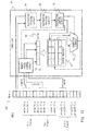
- Fig. 13 illustrates an example of a hardware configuration of a data processing device 9000 for realizing the gather instruction of Conventional Method 1.
- the data processing device 9000 includes a memory 10a and a processor 90.
- the processor 90 includes an instruction fetching circuit 91, an instruction decoding circuit 92, an instruction control circuit 93, an operation circuit 94, a memory access control circuit 95, a buffer 96, and a vector register group 97.
- the instruction fetching circuit 91, the instruction decoding circuit 92, the operation circuit 94, and the vector register group 97 may be the same as those of Fig. 7 .
- the buffer 96 has the same configuration as that of the buffer 461 of Fig. 7 . However, only one buffer 96 is provided.
- the instruction control circuit 93 Upon receiving the gather instruction of Conventional Method 1, the instruction control circuit 93 issues a number of instructions corresponding to (number of structure arrays) x (number of member variables) to the memory access control circuit 95. Moreover, although the memory access control circuit 95 reads a plurality of words collectively, only one data element remains and the other data elements are discarded. The flow will be described below.
- the gather instruction of Conventional Method 1 issues four memory read requests to discontinuous memory areas. This operation is performed on the memory 10a in at least four cycles. Although the memory 10a can read two words in one clock, since the gather instruction can use only one word in that period, one word that is unnecessary is discarded.
- the data elements read earlier from the memory 10a are stored in a buffer until four words of data elements to be stored in the vector register 97 are returned to the processor 90. When one entry of data elements are stored in the buffer 96, the data elements are written to the vector register 97. Specifically, the following operations are performed.
- the memory access control circuit 95 reads array[Q-1].a and array[Q-1].b of the memory 10a collectively and stores array[Q-1].a in the way wQ-1 of the buffer 96 while discarding array[Q-1].b. After that, one entry of data elements are written from the buffer 96 to the corresponding registers of the vector register group 97 (see Fig. 15 ).
- the memory access control circuit 95 performs Q memory accesses and stores array[0].b to array[Q-1] .b to the ways w0 to wQ-1 of the buffer 96 while discarding array[0].a to array[Q-1].a whenever the memory access is performed. After that, one entry of data elements are written from the buffer 96 to other corresponding registers of the vector register group 97 (see Fig. 16 ).
- the processor 90a stores member variables array[0].a and array[0].b of the 0th structure array in one vector register 97 using an instruction of loading a plurality of successive words.
- the processor 90a adds "1" to the index of the structure array and repeats the loading of a plurality of words. In this case, Q load instructions (that is, at least Q clock cycles) are required.
- Embodiment 4 the above problems are solved by adding at least the following configurations to the configuration of Embodiment 2. That is, the control unit writes the respective read data elements so that the storage areas of the data elements in the plurality of storage units correspond to each other. That is, the data elements read from the same storage units in a processor can be written to the positions of the corresponding storage areas of different data sets. Due to this, the results of a vector operation can be returned to the original storage positions and data elements can be written efficiently.
- control unit may preferably read respective data elements from the corresponding areas in the plurality of storage units for each of the plurality of areas in response to an instruction for storing the plurality of vector data elements in the memory.
- the control unit may preferably group the respective data elements read from the corresponding areas to form the data set for each of the plurality of areas.
- the control unit may preferably issue, to the memory, a request for storing respective data elements of the grouped data set in the continuous storage areas in a number corresponding to the number of vector data elements for each of the plurality of areas.
- the processor may further include a vector operation unit that executes a predetermined operation collectively for respective corresponding writing positions in the plurality of storage units, and writes the results of the predetermined operation to the plurality of storage units, and the control unit may start the reading after the vector operation unit writes the results of the predetermined operation.
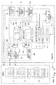
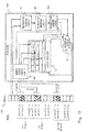
- the memory access control circuit 45a is a circuit that controls a memory access process from the processor 40a to the memory 30.
- the memory access control circuit 45a includes a request issuing unit 450a, switching units 451a and 452a, and a data grouping unit 454.
- the request issuing unit 450a designates the starting memory address A and the number of words N included in the signal SIG3 and issues a memory access (write) request to the memory 30 in order to write the data set generated by the data grouping unit 454.
- the request issuing unit 450a issues a request by adding the size C to the memory address A.
- the request aims to store respective data elements in adjacent areas of the designated N words. In this embodiment, it is assumed that two words are written.
- the instruction control circuit 43a may add the size C to the memory address A.
- Fig. 11 is a flowchart illustrating the flow of the processes of a scatter instruction according to Embodiment 4.
- Fig. 12 is a diagram for describing the concept of the operation of a scatter instruction to a plurality of vector registers according to Embodiment 4. In the following description of Fig. 11 , Fig. 12 is referenced appropriately.
- control unit writes the respective read data elements so that writing positions of the data elements in sort destination storage units correspond to the respective data sets.
- control unit writes the respective read data elements so that the storage areas of the data elements in the plurality of storage units correspond to each other.
- control unit reads respective data elements from the corresponding areas in the plurality of storage units for each of the plurality of areas in response to an instruction for storing a plurality of vector data elements in the memory, the control unit groups the respective data elements read from the corresponding areas to form the data set for each of the plurality of areas, and the control unit issues, to the memory, a request for storing respective data elements of the grouped data set in the continuous storage areas in a number corresponding to the number of vector data elements for each of the plurality of areas.
- a data gathering method for causing a processor to:
Landscapes
- Engineering & Computer Science (AREA)
- Theoretical Computer Science (AREA)
- Software Systems (AREA)
- Physics & Mathematics (AREA)
- General Engineering & Computer Science (AREA)
- General Physics & Mathematics (AREA)
- Databases & Information Systems (AREA)
- Data Mining & Analysis (AREA)
- Mathematical Physics (AREA)
- Computational Linguistics (AREA)
- Complex Calculations (AREA)
- Executing Machine-Instructions (AREA)
- Advance Control (AREA)
Abstract
Description
- This application is based upon and claims the benefit of priority from Japanese patent application No.
2014-108852, filed on May 27, 2014 - The present invention relates to a processor and a data gathering method, and for example, relates to a processor, a data processing device, a data gathering method, and a data writing method for reading or writing a plurality of data sets stored in a memory.
- In recent years, processors capable of executing vector operations have been developed. A vector operation performs a plurality of scalar operations as one operation on vector data elements. Published Japanese Translation of
PCT International Publication for Patent Application, No. 2014-504418 - A gather instruction is an instruction for gathering data values corresponding to a plurality of designated indices of a data array from corresponding areas of a memory. The plurality of data values gathered by the gather instruction is used as an input vector of a subsequent vector operation. A scatter instruction is an instruction for storing data values of vector data in areas of a memory corresponding to designated indices of a data array. The respective elements of the output vector generated by a vector operation can be used as the vector data that is subject to the scatter instruction.
- However, when the gather or scatter instruction is used for the vector operation, processing time may increase and processing efficiency may decrease. This is because only continuous areas of a memory in which a data array is stored can be accessed in one memory access. Due to this, the memory areas in the storage destination of the plurality of memory access target data values are discontinuous (discrete), memory access needs to be performed in respective clusters of continuous areas. That is, although the gather and scatter instructions each are single instructions, the number of memory accesses may increase depending on the storage destination of the data value. Due to this, the preprocessing or post-processing time for the vector operation increases.
- Other objects and new features will become apparent from the description of the present specification and the accompanying drawings.
- According to an embodiment of the present invention, a processor loads or stores a plurality of data elements included in a plurality of data sets between a memory and a storage unit in a processor by changing the storage order of the data elements.
- A method and a system with which the processor according to the embodiment is replaced, a program for causing a computer to execute the process of the device or a portion of the device, an imaging apparatus including the device, and the like are also effective as aspects of the present invention.
- According to the embodiment, the process of loading or storing data between the memory and the storage unit in the processor can be performed efficiently.
- The above and other aspects, advantages and features will be more apparent from the following description of certain embodiments taken in conjunction with the accompanying drawings, in which:
-
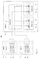
Fig. 1 is a block diagram illustrating a configuration of a data processing device including a processor according toEmbodiment 1; -
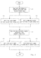
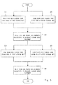
Fig. 2 is a flowchart illustrating the flow of the processes of a data gathering method according toEmbodiment 1; -
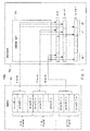
Fig. 3 is a block diagram illustrating another configuration of a data processing device including the processor according toEmbodiment 1; -
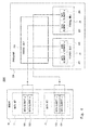
Fig. 4 is a block diagram illustrating a configuration of a data processing device including a processor according toEmbodiment 2; -
Fig. 5 is a flowchart illustrating the flow of the processes of a data writing method according toEmbodiment 2; -
Fig. 6 is a block diagram illustrating another configuration of a data processing device including the processor according toEmbodiment 2; -
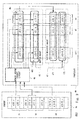
Fig. 7 is a block diagram illustrating a configuration of a data processing device including a processor according to Embodiment 3; -
Fig. 8 is a flowchart illustrating the flow of the processes of a gather instruction according to Embodiment 3; -
Fig. 9 is a diagram for describing the concept of the operation of a gather instruction to a plurality of vector registers according to Embodiment 3; -
Fig. 10 is a block diagram illustrating the configuration of a data processing device including a processor according to Embodiment 4; -
Fig. 11 is a flowchart illustrating the flow of the processes of a scatter instruction according to Embodiment 4; -
Fig. 12 is a diagram for describing the concept of the operation of a scatter instruction to a plurality of vector registers according to Embodiment 4; -
Fig. 13 is a diagram for describing the concept of a gather instruction according to the related art; -
Fig. 14 is a diagram for describing the concept of a scatter instruction according to the related art; -
Fig. 15 is a diagram for describing the concept of the operation of a gather instruction to a plurality of vector registers according to the related art; -
Fig. 16 is a diagram for describing the concept of the operation of a gather instruction to a plurality of vector registers according to the related art; -
Fig. 17 is a diagram for describing the concept of the operation of a load instruction of loading a plurality of words according to the related art; and -
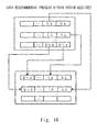
Fig. 18 is a diagram for describing the concept of the operation of a process of rearranging data in a vector register according to the related art. - Hereinafter, specific embodiments to which means for solving the above problems are employed will be described in detail with reference to the drawings. In the respective drawings, components having the same function are denoted by the same reference symbols, and redundant description thereof will be omitted as appropriate for the clarity of the explanation.
- In the embodiments described below, the invention will be described in a plurality of sections or embodiments when required as a matter of convenience. However, these sections or embodiments are not irrelevant to each other unless otherwise stated, and the one relates to the entire or a part of the other as a modification example, an application example, details, or a supplementary explanation thereof. Moreover, in the embodiments described below, when referring to the number of elements (including number of pieces, values, amount, range, and the like), the number of the elements is not limited to a specific number unless otherwise stated or except the case where the number is apparently limited to a specific number in principle. The number larger or smaller than the specified number is also applicable.
-
Fig. 1 is a block diagram illustrating a configuration of adata processing device 1000 including aprocessor 20 according toEmbodiment 1. Thedata processing device 1000 includes amemory 10 and theprocessor 20. Thememory 10 is a storage device in which data sets 11 and 12 and the like are stored. Thememory 10 corresponds to a so-called main storage device and is present outside theprocessor 20. Thememory 10 is connected to theprocessor 20 by a memory bus (not illustrated). - The
data set 11 includes a plurality of data elements such as data element a 101 anddata element b 102. Here, it is assumed that the data element a 101 and thedata element b 102 are stored in adjacent storage areas in thememory 10. Moreover, thedata set 12 includes a plurality of data elements such asdata element c 103 anddata element d 104. Here, it is assumed that thedata element c 103 and thedata element d 104 are stored in adjacent storage areas in thememory 10. - The
processor 20 includes astorage unit 21, astorage unit 22, and acontrol unit 23. Thestorage units storage unit 21 is divided into at leastareas storage unit 21 is associated with the data element a 101 and thedata element c 103. Moreover, thestorage unit 22 is divided into at leastareas storage unit 22 is associated with thedata element b 102 and thedata element d 104. - The
control unit 23 reads the plurality of data elements stored in the adjacent storage areas from thememory 10 collectively for each data set. Here, "reads ... collectively" corresponds to reading a plurality of words in one memory access process from thecontrol unit 23 to thememory 10. For example, in one memory access process, thecontrol unit 23 reads the data element a 101 and thedata element b 102 included in the data set 11 from thememory 10. In another memory access process, thecontrol unit 23 reads the data element c 103 and thedata element d 104 included in the data set 12 from thememory 10. - The
control unit 23 sorts the read data elements to a storage unit corresponding to the data element among the plurality ofstorage units control unit 23 sorts and writes the data element a 101 and thedata element b 102 read for the data set 11 to thestorage units control unit 23 sorts and writes the data element c 103 and thedata element d 104 read for the data set 12 to thestorage units -
Fig. 2 is a flowchart illustrating the flow of the processes of a data gathering method according toEmbodiment 1. First, thecontrol unit 23 of theprocessor 20 reads first and second data elements (for example, the data element a 101 and the data element b 102) stored in adjacent areas of thememory 10 collectively from the memory 10 (S11). - Subsequently, the
control unit 23 writes the read first data element to a first area (for example, the area 201) of a first storage unit (for example, the storage unit 21) (S12). Moreover, thecontrol unit 23 writes the read second data element to a first area (for example, the area 202) of a second storage unit (for example, the storage unit 22) (S13). Thearea 202 may be an area corresponding to thearea 201. Moreover, thecontrol unit 23 may write the read second data element to thearea 204 of thestorage unit 22. - Subsequently, the
control unit 23 reads third and fourth data elements (for example, the data element c 103 and the data element d 104) stored in adjacent areas of thememory 10 collectively from the memory 10 (S14). - The
control unit 23 writes the read third data element to a second area (for example, the area 203) of the first storage unit (S15). Moreover, thecontrol unit 23 writes the read fourth data element to a second area (for example, the area 204) of the second storage unit (S16). Thearea 204 may be an area corresponding to thearea 203. Here, thecontrol unit 23 may write the read third data element in an area other than the area to which data has been written at least in step S12 among the area of the first storage unit. Similarly, thecontrol unit 23 may write the read fourth data element to an area other than the area to which data has been written at least in step S13 among the areas of the second storage unit. -
Fig. 3 is a block diagram illustrating a configuration of adata processing device 1000a including aprocessor 20a according toEmbodiment 1. Theprocessor 20a is used when the configuration of theprocessor 20 ofFig. 1 is applied to a case in which N words (N is a natural number of 2 or more) are read collectively from each of three or more data sets and areas of storage destination storage units are associated as ways. Q data arrays (array[0] to array[Q-1]) (Q is a natural number of 2 or more) are stored in amemory 10a. Each data array includes data elements a, b, ..., and p. - The
processor 20a includes acontrol unit 23a and registers rgk, rgk+1, ..., and rgk+N-1 (k is a natural number and N is a natural number of 2 or more). Here, it is assumed that each of the registers rgk to rgk+N-1 is divided into a plurality of ways w0, w1, ..., and wQ-1 which are areas, and the same ways of the respective registers correspond to each other. Theprocessor 20a reads N words collectively from a data array array[0] and writes the respective data elements to the way w0 of the respective registers rgk to rgk+N-1. Moreover, theprocessor 20a reads N words collectively from a data array array[1] and writes the respective data elements to the way w1 of the registers rgk to rgk+N-1. Theprocessor 20a performs the same processes on data arrays array [2] to array[Q-1]. For example, theprocessor 20a reads N words collectively from the data array array[Q-1] and writes the respective data elements to the way wQ-1 of the respective registers rgk to rgk+N-1. - In this way, according to
Embodiment 1, when gathering a plurality of data groups stored in discontinuous areas of thememory 10, such as, for example, a group formed by the data element a 101 and the data element c 103 and a group formed by the data element b 102 and thedata element d 104, the time required for a data loading process can be reduced. This is because the results of accessing continuous (adjacent) memory areas are sorted and stored in the first and second storage units in the processor, and it is therefore not necessary to perform memory accesses individually. Moreover, since the read data groups are sorted and stored to the corresponding storage units, it is not necessary to execute a process of rearranging the read data groups additionally. Thus, the process of loading data between the memory and the storage unit in the processor can be performed efficiently. -
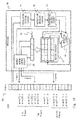
Fig. 4 is a block diagram illustrating a configuration of adata processing device 2000 including aprocessor 20b according toEmbodiment 2. Thedata processing device 2000 includes amemory 10 and theprocessor 20b. Thememory 10 is the same as that ofFig. 1 , and redundant description thereof will be omitted. - The
processor 20b includes astorage unit 21, astorage unit 22, and acontrol unit 23b. Thestorage units Fig. 1 . That is, thestorage unit 21 is divided into at leastareas storage unit 22 is divided into at leastareas storage units areas storage unit 21, respectively. Moreover, the data element b and the data element d are stored in theareas storage unit 22, respectively. - The
control unit 23b reads the respective data elements stored in the corresponding areas in thestorage units storage units area 201 of thestorage unit 21 corresponds to thearea 202 of thestorage unit 22, and thearea 203 of thestorage unit 21 corresponds to thearea 204 of thestorage unit 22. Thus, for example, thecontrol unit 23b reads the data element a and the data element b from theareas control unit 23b puts the data elements read from the respective corresponding areas together to form a data set. For example, thecontrol unit 23b puts the data element a and the data element b together to form a data set. Thecontrol unit 23b writes the respective data elements in the data set to adjacent storage areas in thememory 10. For example, thecontrol unit 23b writes the data element a 101 and thedata element b 102 to the storage areas in thememory 10, corresponding to the data element a 101 and thedata element b 102 of thedata set 11. Thecontrol unit 23b also reads the data elements stored in theareas memory 10 corresponding to thedata set 12. -
Fig. 5 is a flowchart illustrating the flow of the processes of a data writing method according toEmbodiment 2. First, thecontrol unit 23b of theprocessor 20b reads a first data element (for example, the data element a) from a first area (for example, the area 201) of a first storage unit (for example, the storage unit 21) (S21). Moreover, thecontrol unit 23b reads a second data element (for example, the data element b) from a first area (for example, the area 202) of a second storage unit (for example, the storage unit 22) (S22). Thearea 202 may be an area corresponding to thearea 201. Moreover, thecontrol unit 23b may read the second data element from thearea 204 of thestorage unit 22. - Subsequently, the
control unit 23b writes the first and second data elements collectively to adjacent storage areas in the memory 10 (S23). For example, as described above, in one memory access process, thecontrol unit 23b writes the data element a and the data element b to the storage areas in thememory 10 corresponding to the data element a 101 and thedata element b 102 of thedata set 11, respectively. - Subsequently, the
control unit 23b reads a third data element (for example, the data element c) from a second area (for example, the area 203) of the first storage unit (S24). Moreover, thecontrol unit 23b reads a fourth data element (for example, the data element d) from a second area (for example, the area 204) of the second storage unit (S25). Thearea 204 may be an area corresponding to thearea 203. Here, thecontrol unit 23b may read the third data element from an area other than the area from which data has been read at least in step S21 among the areas of the first storage unit. Similarly, thecontrol unit 23b may read the fourth data element from an area other than the area from which data has been read at least in step S22 among the areas of the second storage unit. - The
control unit 23b writes the third and fourth data elements collectively to adjacent storage areas in the memory 10 (S26). For example, in another memory access process different from that of step S23, thecontrol unit 23b writes the data element c and the data element d to storage areas in thememory 10 corresponding to the data element c 103 and thedata element d 104 of thedata set 12. Here, it is assumed that the write destination storage areas in step S26 are different from the write destination storage areas in step S23. -
Fig. 6 is a block diagram illustrating a configuration of aparity data 2000a including aprocessor 20c according toEmbodiment 2. Theprocessor 20c is used when the configuration of theprocessor 20b ofFig. 4 is applied to a case in which N words are read from three or more registers and written collectively to thememory 10a and areas of read source storage units (registers) are associated as ways. - The
processor 20c includes acontrol unit 23c and registers rgk to rgk+N-1. Here, the registers rgk to rgk+N-1 are the same as those ofFig. 3 . However, it is assumed that data elements are stored in advance in ways w0 to wQ-1 of the registers rgk to rgk+N-1. Theprocessor 20c reads data elements from the registers rgk to rgk+N-1 collectively for each way and puts the data elements read for each way together to form a data set. Theprocessor 20c writes the respective data elements in the data set to adjacent storage areas in thememory 10a. For example, theprocessor 20c reads data elements from the way w0 of the respective registers rgk to rgk+N-1 and writes N words to array[0].a to array[0].n of thememory 10a in one memory access process. Theprocessor 20c reads data elements similarly for each of the ways w1 to wQ-1 and writes the data elements in the same adjacent storage areas of the data set for respective ways. - In this way, according to
Embodiment 2, when writing data groups stored in a plurality of storage units, such as, for example, a group formed by the data elements a and b and a group formed by the data elements c and d, collectively as one data set, the time required for a data storing process can be reduced. This is because the respective data elements read individually from different storage units are written collectively to continuous (adjacent) areas, and it is therefore not necessary to perform memory access processes individually for respective data elements. Moreover, since data elements are read from the corresponding areas in a plurality of storage units, it is not necessary to execute a process of rearranging the read data elements. Thus, the process of storing data between the memory and the storage unit in the processor can be performed efficiently. - Here, a problem to be solved by this embodiment will be described again. First, it is assumed that data elements of a structure including a plurality of member variables are continuously stored in a memory as structure arrays. In this case, a vector operation may be performed on the same member variables of the plurality of structure arrays. In order to gather such vector data elements from the memory, a read instruction of reading vector data elements from the memory for respective member variables of each structure generally needs to be issued to a processor. Moreover, in order to store the plurality of vector data elements obtained as the results of the vector operation in a memory, a write instruction of writing vector data elements to the memory from registers in a processor for respective member variables of each structure generally needs to be issued to the processor.
- In this respect, in the related art, gather and scatter instructions are often implemented in a processor as
Conventional Method 1. In general, when a single gather or scatter instruction is issued to a processor, a plurality of memory access instructions is issued from the processor to a memory. For example, the following processes are performed. - (1) Upon receiving a gather instruction, the processor issues a plurality of memory access instructions for data elements stored in discontinuous areas and loads the respective read data elements to one register.
- (2) The processor applies a vector operation to the respective data elements loaded to the register as a plurality of vector data elements.
- (3) Upon receiving a scatter instruction, the processor reads the respective data elements of the register individually, issues a memory access instruction for writing the data elements to a memory whenever the data elements are read, and writes the data elements to memory addresses of discontinuous areas.
- Thus, even when a hardware that forms the processor has a memory bandwidth capable of accessing successive N words, according to
Conventional Method 1, since the scatter and gather instructions access data elements in discontinuous areas individually, it is difficult to utilize the bandwidth sufficiently. Thus, inConventional Method 1, memory access processes are performed in a number of times corresponding to the number of structures and member variables. Moreover, the processing time increases and the processing efficiency decreases. -
Conventional Method 2 uses a memory access instruction for a plurality of words by utilizing a bandwidth capable of accessing a plurality of words. That is, inConventional Method 2, in a single memory access process for a plurality of words, data groups stored in continuous areas of a memory are temporarily stored in vector registers. In this stage, data groups of respective structures are stored in the respective vector registers. Thus, after that, a rearrangement process is executed so that the same member variables of the respective structures are stored in the same vector registers. Thus, it is necessary to insert an unnecessary instruction of the rearrangement process within vector registers before and after the vector operation is applied. Thus, inConventional Method 2, the processing time increases and the processing efficiency decreases. - Therefore, in Embodiment 3, the above problems are solved by adding at least the following configurations to the configuration of
Embodiment 1. That is, the control unit writes the read data elements so that writing positions of the data elements in the sort destination storage units correspond to the respective data sets. For example, the data elements of the plurality of words read from a memory by a first memory access are sorted and stored in a plurality of storage units, and in this case, the data elements are written to the same way. The data elements read collectively and simultaneously by subsequent memory accesses (that is, from the same data set) are written to the same way different from the way used in the first memory access. By doing so, the data groups written to the respective storage units in the processor can be used for the vector operation as vector data elements as they are, and data can be gathered more efficiently. - The control unit may preferably sort the respective data elements read from the memory to any one of the plurality of storage units according to the order of the adjacent storage areas in the memory. In this case, the control unit may preferably write the sorted data elements to the respective sort destination storage units. For example, when data elements are stored in a memory according to the order of definitions of the member variables of a structure, the order of definitions is associated with a sort destination storage unit. By doing so, the order of reading data from a memory can be easily associated with a sort destination storage unit, and the configuration of the processor can be simplified.
- The control unit may preferably issue, to the memory, a request for reading the plurality of data elements from the continuous storage areas in a number corresponding to the number of a plurality of vector data elements for each data set, in response to an instruction for gathering the vector data elements. In this case, the control unit may preferably sort the data elements read from the memory in response to the request to any one of the plurality of storage units for each request. By doing so, for example, the memory access and the sorting of storage units according to this embodiment can be applied to a gather instruction.
- Further, the control unit may issue the request in response to an instruction for gathering the plurality of vector data elements, designate the writing position for each data set, and write the respective sorted data elements to the designated writing positions in the respective sort destination storage units. For example, when a way is designated as the writing position, data elements can be easily written to the corresponding areas in the sort destination storage units in response to a memory access to each data set.
- Alternatively, the plurality of storage units each may include a plurality of buffers corresponding to the storage areas of the respective data elements in the data set, and a plurality of registers corresponding to the buffers. The control unit may designate, among the plurality of buffers, different write destination buffers for respective storage areas to sort and write the respective data elements in the designated buffer, read the plurality of data elements in all of the plurality of data sets, and then, write all data elements written to each of the plurality of buffers collectively to the register corresponding to the buffer. In this manner, when data elements are individually written to buffers which can be flexibly rewritten in respective area units, the number of writing operations on a vector register in which it is difficult to rewrite data in respective area units can be reduced and the processing efficiency can be increased.
- Further, the processor may further include a vector operation unit that executes a predetermined operation collectively for respective corresponding writing positions in the plurality of storage units. By doing so, the gathered data groups can be efficiently utilized for the vector operation.
- Further, the vector operation unit may execute the predetermined operation on at least two of the plurality of storage units. For example, even when a vector operation is performed on data elements stored in areas which are not necessarily adjacent in a data set, data elements which are not used for the vector operation may be read collectively and such data elements themselves may not be subject to the vector operation. By doing so, a memory access process of reading a plurality of words can be performed efficiently.
- Further, the plurality of data sets may preferably be a structure which uses the plurality of data elements as member variables, and the plurality of storage units may preferably be associated with the member variables. The control unit may preferably sort and write the respective read data elements to the plurality of storage units associated with the member variables. By doing so, a vector operation can be performed efficiently on a structure defined including a plurality of data types.
- Next, a gather instruction of gathering data elements to a plurality of vector registers according to Embodiment 3 will be described in detail.
Fig. 7 is a block diagram illustrating a configuration of adata processing device 3000 including aprocessor 40 according to Embodiment 3. Thedata processing device 3000 is an improvement example of thedata processing device 1000 according toEmbodiment 1 and includes amemory 30 and theprocessor 40. Thememory 30 has the same configuration as thememory 10 andstructures structure 31 or the like is a structure having P member variables (P is a natural number of 2 or more) and Q data elements (Q is a natural number of 2 or more) are stored in thememory 30. A structure is a variable having variable definitions of a plurality of data types. When thestructure 31 or the like is expressed in C language, the structure can be defined as the following structure arrays.
      struct {
            int a,
            int b,
            ...
            int p;
      } z[Q];
- Starting memory address A of read source memory (corresponding to starting storage area of structure array, for example)
- Starting register number k of write destination (k corresponds to number Q of read target structures and is a natural number equal to or smaller than an upper limit number of ways W)
- Number of words N for successive memory accesses (N is a natural number of 2 or more and P or smaller)
- Size C for updating memory addresses (C is the same as structure size P)
- Starting memory address A of write destination memory (corresponding to starting storage area of structure array, for example)
- Starting register number k of read source (k corresponds to number Q of reading target structures and is a natural number equal to or smaller than an upper limit number of ways W)
- Number of words N for successive memory accesses (N is a natural number of 2 or more and P or smaller)
- Size C for updating memory addresses (C is the same as structure size P)
- a plurality of storage units associated with a plurality of data elements included in a data set; and
- a control unit that reads the plurality of data elements stored in adjacent storage areas from a memory, in which a plurality of the data sets is stored, collectively for respective data sets, sorts the respective read data elements to a storage unit corresponding to the data element among the plurality of storage units, and writes the data elements to the respective data sets.
the control unit writes the respective read data elements so that writing positions of the data elements in sort destination storage units correspond to the respective data sets.
the control unit sorts the respective data elements read from the memory to any one of the plurality of storage units according to the order of the adjacent storage areas in the memory, and
the control unit writes the sorted data elements to the respective sort destination storage units.
the control unit issues, to the memory, a request for reading the plurality of data elements from the continuous storage areas in a number corresponding to the number of a plurality of vector data elements for each data set, in response to an instruction for gathering the vector data elements, and
the control unit sorts the data elements read from the memory in response to the request to any one of the plurality of storage units for each request.
the control unit issues the request and designates the writing position for each data set in response to the instruction for gathering the plurality of vector data elements, and
the control unit writes the respective sorted data elements to the designated writing positions in the respective sort destination storage units.
the plurality of storage units each include a plurality of buffers corresponding to the storage areas of the respective data elements in the data set, and a plurality of registers corresponding to the buffers,
the control unit designates, among the plurality of buffers, different write destination buffers for respective storage areas to sort and write the respective data elements in the designated buffer, and
the control unit reads the plurality of data elements in all of the plurality of data sets, and then, writes all data elements written to each of the plurality of buffers collectively to the register corresponding to the buffer.
- a vector operation unit that executes a predetermined operation collectively for respective corresponding writing positions in the plurality of storage units.
the vector operation unit executes the predetermined operation on at least two of the plurality of storage units.
the plurality of data sets is a structure which uses the plurality of data elements as member variables,
the plurality of storage units is associated with the member variables, and
the control unit sorts and writes the respective read data elements to the plurality of storage units associated with the member variables.
- a plurality of storage units each divided into a plurality of areas in which a plurality of data elements is stored; and
- a control unit that reads respective data elements stored in corresponding areas in the respective storage units, from each of the plurality of storage units, puts the read data elements together to form a data set for each of the corresponding areas, and writes the respective data elements in the data set to adjacent storage areas in a memory.
the control unit writes the respective read data elements so that the storage areas of the data elements in the plurality of storage units correspond to each other.
the control unit reads respective data elements from the corresponding areas in the plurality of storage units for each of the plurality of areas in response to an instruction for storing a plurality of vector data elements in the memory,
the control unit groups the respective data elements read from the corresponding areas to form the data set for each of the plurality of areas, and
the control unit issues, to the memory, a request for storing respective data elements of the grouped data set in the continuous storage areas in a number corresponding to the number of vector data elements for each of the plurality of areas.
the control unit issues the request and designates the area for each of the plurality of areas in response to the instruction for storing the plurality of vector data elements in the memory, and
the control unit reads the respective data elements from each of the plurality of storage units using the designated area as the corresponding area.
the plurality of storage units each include a plurality of registers capable of reading and writing data in the entire divided area units, and a plurality of buffers which correspond to the respective registers and are capable of reading and writing data in the individual area units,
the control unit reads all of the plurality of data elements stored in each of the plurality of registers and writes the data elements collectively to the respective buffers corresponding to the respective registers,
the control unit reads, for each of corresponding areas in the registers, the respective data elements stored in the areas of the respective buffers,
the control unit puts the read data elements together to form a writing data set for each of the corresponding areas, and
the control unit writes the respective data elements in the data set to adjacent storage areas in the memory.
- a vector operation unit that executes a predetermined operation collectively for respective corresponding writing positions in the plurality of storage units, and writes the results of the predetermined operation to the plurality of storage units, wherein
- the control unit starts the reading after the vector operation unit writes the results of the predetermined operation.
- read first and second data elements stored in adjacent areas of a memory collectively from the memory;
- write the read first data element to a first area of a first storage unit, and write the read second data element to an area of a second storage unit corresponding to the first area;
- read third and fourth data elements stored in adjacent areas of the memory collectively from the memory; and
- write the read third data element to a second area of the first storage unit, and write the read fourth data element to an area of the second storage unit corresponding to the second area.
- read a first data element from a first area of a first storage unit;
- read a second data element from an area of a second storage unit corresponding to the first area;
- write the first and second data elements collectively to adjacent storage areas in a memory;
- read a third data element from a second area of the first storage unit;
- read a fourth data element from an area of the second storage unit corresponding to the second area; and
- write the third and fourth data elements collectively to adjacent storage areas in the memory other than the storage areas.
- a memory in which a plurality of data sets is stored; and
- a processor including a plurality of storage units associated with a plurality of data elements included in each of the plurality of data sets, wherein
- the processor reads the plurality of data elements stored in adjacent storage areas collectively from the memory for each of the data sets; and
- the processor sorts and writes the respective read data elements to a storage unit corresponding to the data element among the plurality of storage units.
- a memory; and
- a processor including a plurality of storage units each divided into a plurality of areas in which a plurality of data elements is stored; and a control unit that reads respective data elements stored in corresponding areas in the respective storage units, from each of the plurality of storage units, puts the read data elements together to form a data set for each of the corresponding areas, and writes the respective data elements in the data set to adjacent storage areas in a memory.
Claims (16)
- A processor comprising:a plurality of storage units associated with a plurality of data elements included in a data set; anda control unit that reads the plurality of data elements stored in adjacent storage areas from a memory, in which a plurality of the data sets is stored, collectively for respective data sets, sorts the respective read data elements to a storage unit corresponding to the data element among the plurality of storage units, and writes the data elements to the respective data sets.
- The processor according to Claim 1, wherein
the control unit writes the respective read data elements so that writing positions of the data elements in sort destination storage units correspond to the respective data sets. - The processor according to Claim 1 or 2, wherein
the control unit sorts the respective data elements read from the memory to any one of the plurality of storage units according to the order of the adjacent storage areas in the memory, and
the control unit writes the sorted data elements to the respective sort destination storage units. - The processor according to one of Claims 1 to 3, wherein
the control unit issues, to the memory, a request for reading the plurality of data elements from the continuous storage areas in a number corresponding to the number of a plurality of vector data elements for each data set, in response to an instruction for gathering the vector data elements, and
the control unit sorts the data elements read from the memory in response to the request to any one of the plurality of storage units for each request. - The processor according to one of Claims 1 to 4, wherein
the control unit issues the request and designates the writing position for each data set in response to the instruction for gathering the plurality of vector data elements, and
the control unit writes the respective sorted data elements to the designated writing positions in the respective sort destination storage units. - The processor according to one of Claims 2 to 5, wherein
the plurality of storage units each include a plurality of buffers corresponding to the storage areas of the respective data elements in the data set, and a plurality of registers corresponding to the buffers,
the control unit designates, among the plurality of buffers, different write destination buffers for respective storage areas to sort and write the respective data elements in the designated buffer, and
the control unit reads the plurality of data elements in all of the plurality of data sets, and then, writes all data elements written to each of the plurality of buffers collectively to the register corresponding to the buffer. - The processor according to one of Claims 2 to 6, further comprising a vector operation unit that executes a predetermined operation collectively for respective corresponding writing positions in the plurality of storage units.
- The processor according to Claim 7, wherein
the vector operation unit executes the predetermined operation on at least two of the plurality of storage units. - The processor according to one of Claims 1 to 8, wherein
the plurality of data sets is a structure which uses the plurality of data elements as member variables,
the plurality of storage units is associated with the member variables, and
the control unit sorts and writes the respective read data elements to the plurality of storage units associated with the member variables. - A processor comprising:a plurality of storage units each divided into a plurality of areas in which a plurality of data elements is stored; anda control unit that reads respective data elements stored in corresponding areas in the respective storage units, from each of the plurality of storage units, puts the read data elements together to form a data set for each of the corresponding areas, and writes the respective data elements in the data set to adjacent storage areas in a memory.
- The processor according to Claim 10, wherein
the control unit writes the respective read data elements so that the storage areas of the data elements in the plurality of storage units correspond to each other. - The processor according to Claim 10 or 11, wherein
the control unit reads respective data elements from the corresponding areas in the plurality of storage units for each of the plurality of areas in response to an instruction for storing a plurality of vector data elements in the memory,
the control unit groups the respective data elements read from the corresponding areas to form the data set for each of the plurality of areas, and
the control unit issues, to the memory, a request for storing respective data elements of the grouped data set in the continuous storage areas in a number corresponding to the number of vector data elements for each of the plurality of areas. - The processor according to one of Claims 10 to 12, wherein
the control unit issues the request and designates the area for each of the plurality of areas in response to the instruction for storing the plurality of vector data elements in the memory, and
the control unit reads the respective data elements from each of the plurality of storage units using the designated area as the corresponding area. - The processor according to one of Claims 11 to 13, wherein
the plurality of storage units each include a plurality of registers capable of reading and writing data in the entire divided area units, and a plurality of buffers which correspond to the respective registers and are capable of reading and writing data in the individual area units,
the control unit reads all of the plurality of data elements stored in each of the plurality of registers and writes the data elements collectively to the respective buffers corresponding to the respective registers,
the control unit reads, for each of corresponding areas in the registers, the respective data elements stored in the areas of the respective buffers,
the control unit puts the read data elements together to form a writing data set for each of the corresponding areas, and
the control unit writes the respective data elements in the data set to adjacent storage areas in the memory. - The processor according to one of Claims 11 to 14, further comprising a vector operation unit that executes a predetermined operation collectively for respective corresponding writing positions in the plurality of storage units, and writes the results of the predetermined operation to the plurality of storage units, wherein
the control unit starts the reading after the vector operation unit writes the results of the predetermined operation. - A data gathering method for causing a processor to:read first and second data elements stored in adjacent areas of a memory collectively from the memory;write the read first data element to a first area of a first storage unit, and write the read second data element to an area of a second storage unit corresponding to the first area;read third and fourth data elements stored in adjacent areas of the memory collectively from the memory; andwrite the read third data element to a second area of the first storage unit, and write the read fourth data element to an area of the second storage unit corresponding to the second area.
Applications Claiming Priority (1)
| Application Number | Priority Date | Filing Date | Title |
|---|---|---|---|
| JP2014108852A JP6253514B2 (en) | 2014-05-27 | 2014-05-27 | Processor |
Publications (1)
| Publication Number | Publication Date |
|---|---|
| EP2950202A1 true EP2950202A1 (en) | 2015-12-02 |
Family
ID=53174845
Family Applications (1)
| Application Number | Title | Priority Date | Filing Date |
|---|---|---|---|
| EP15167062.7A Withdrawn EP2950202A1 (en) | 2014-05-27 | 2015-05-11 | Processor and data gathering method |
Country Status (4)
| Country | Link |
|---|---|
| US (1) | US10235398B2 (en) |
| EP (1) | EP2950202A1 (en) |
| JP (1) | JP6253514B2 (en) |
| CN (1) | CN105320469B (en) |
Cited By (7)
| Publication number | Priority date | Publication date | Assignee | Title |
|---|---|---|---|---|
| WO2017112177A1 (en) | 2015-12-21 | 2017-06-29 | Intel Corporation | Instructions and logic for lane-based strided scatter operations |
| GB2552153A (en) * | 2016-07-08 | 2018-01-17 | Advanced Risc Mach Ltd | An apparatus and method for performing a rearrangement operation |
| EP3391195A4 (en) * | 2015-12-18 | 2019-07-17 | Intel Corporation | INSTRUCTIONS AND LOGIC FOR STRIDE MEMORY OPERATIONS BASED ON TRACKS |
| EP3398059A4 (en) * | 2015-12-30 | 2019-07-24 | Intel Corporation | Systems, apparatuses, and methods for lane-based strided gather |
| WO2019168657A1 (en) * | 2018-03-01 | 2019-09-06 | Qualcomm Incorporated | Pack and unpack network and method for variable bit width data formats |
| EP3629157A3 (en) * | 2018-09-28 | 2020-06-17 | INTEL Corporation | Systems for performing instructions for fast element unpacking into 2-dimensional registers |
| US10963251B2 (en) | 2016-07-08 | 2021-03-30 | Arm Limited | Vector register access |
Families Citing this family (21)
| Publication number | Priority date | Publication date | Assignee | Title |
|---|---|---|---|---|
| US9875214B2 (en) * | 2015-07-31 | 2018-01-23 | Arm Limited | Apparatus and method for transferring a plurality of data structures between memory and a plurality of vector registers |
| US10509726B2 (en) | 2015-12-20 | 2019-12-17 | Intel Corporation | Instructions and logic for load-indices-and-prefetch-scatters operations |
| US20170177363A1 (en) * | 2015-12-22 | 2017-06-22 | Intel Corporation | Instructions and Logic for Load-Indices-and-Gather Operations |
| US10019262B2 (en) * | 2015-12-22 | 2018-07-10 | Intel Corporation | Vector store/load instructions for array of structures |
| US20170192783A1 (en) * | 2015-12-30 | 2017-07-06 | Elmoustapha Ould-Ahmed-Vall | Systems, Apparatuses, and Methods for Stride Load |
| US20170192782A1 (en) * | 2015-12-30 | 2017-07-06 | Robert Valentine | Systems, Apparatuses, and Methods for Aggregate Gather and Stride |
| US10901940B2 (en) | 2016-04-02 | 2021-01-26 | Intel Corporation | Processors, methods, systems, and instructions to atomically store to memory data wider than a natively supported data width |
| US20170371657A1 (en) * | 2016-06-24 | 2017-12-28 | Qualcomm Incorporated | Scatter to gather operation |
| CN106126195B (en) * | 2016-06-30 | 2019-01-15 | 联想(北京)有限公司 | A kind of information processing method and electronic equipment |
| US10776118B2 (en) * | 2016-09-09 | 2020-09-15 | International Business Machines Corporation | Index based memory access using single instruction multiple data unit |
| US10809978B2 (en) * | 2017-06-02 | 2020-10-20 | Texas Instruments Incorporated | Merge sort accelerator |
| JP7035751B2 (en) * | 2018-04-12 | 2022-03-15 | 富士通株式会社 | Code conversion device, code conversion method, and code conversion program |
| US10795678B2 (en) * | 2018-04-21 | 2020-10-06 | Microsoft Technology Licensing, Llc | Matrix vector multiplier with a vector register file comprising a multi-port memory |
| WO2019244656A1 (en) * | 2018-06-22 | 2019-12-26 | 日本電気株式会社 | Storage device |
| JP2020004247A (en) * | 2018-06-29 | 2020-01-09 | ソニー株式会社 | Information processing apparatus, information processing method, and program |
| US20200004535A1 (en) * | 2018-06-30 | 2020-01-02 | Intel Corporation | Accelerator apparatus and method for decoding and de-serializing bit-packed data |
| US20200097291A1 (en) * | 2018-09-24 | 2020-03-26 | Intel Corporation | Apparatus and method for tile gather and tile scatter |
| US10838734B2 (en) | 2018-09-24 | 2020-11-17 | Intel Corporation | Apparatus and method for processing structure of arrays (SoA) and array of structures (AoS) data |
| CN111949318B (en) * | 2019-05-17 | 2024-07-23 | 上海寒武纪信息科技有限公司 | Instruction processing method, device and related products |
| WO2020250419A1 (en) * | 2019-06-14 | 2020-12-17 | 日本電気株式会社 | Control device, control method, and non-transitory computer-readable medium in which control program is stored |
| US12423099B2 (en) * | 2022-12-02 | 2025-09-23 | SiFive, Inc. | Stateful vector group permutation with storage reuse |
Citations (5)
| Publication number | Priority date | Publication date | Assignee | Title |
|---|---|---|---|---|
| US20020032710A1 (en) * | 2000-03-08 | 2002-03-14 | Ashley Saulsbury | Processing architecture having a matrix-transpose capability |
| US20040236920A1 (en) * | 2003-05-20 | 2004-11-25 | Sheaffer Gad S. | Methods and apparatus for gathering and scattering data associated with a single-instruction-multiple-data (SIMD) operation |
| WO2007103195A2 (en) * | 2006-03-06 | 2007-09-13 | Analog Devices. Inc. | Improved permutable address processor and method |
| US20100318766A1 (en) * | 2009-06-16 | 2010-12-16 | Fujitsu Semiconductor Limited | Processor and information processing system |
| JP2014504418A (en) | 2010-12-22 | 2014-02-20 | インテル・コーポレーション | Vector conflict instructions |
Family Cites Families (5)
| Publication number | Priority date | Publication date | Assignee | Title |
|---|---|---|---|---|
| WO1989003091A1 (en) * | 1987-09-25 | 1989-04-06 | Hitachi, Ltd. | Method of sorting vector data and a vector processor adapted thereto |
| GB2409066B (en) * | 2003-12-09 | 2006-09-27 | Advanced Risc Mach Ltd | A data processing apparatus and method for moving data between registers and memory |
| JP5165662B2 (en) * | 2009-10-27 | 2013-03-21 | 株式会社高速屋 | Bit string key classification / distribution device, classification / distribution method and program |
| JP5658556B2 (en) | 2010-12-24 | 2015-01-28 | 富士通株式会社 | Memory control device and memory control method |
| US9274591B2 (en) * | 2013-07-22 | 2016-03-01 | Globalfoundries Inc. | General purpose processing unit with low power digital signal processing (DSP) mode |
-
2014
- 2014-05-27 JP JP2014108852A patent/JP6253514B2/en active Active
-
2015
- 2015-04-23 US US14/694,026 patent/US10235398B2/en active Active
- 2015-05-11 EP EP15167062.7A patent/EP2950202A1/en not_active Withdrawn
- 2015-05-26 CN CN201510276210.8A patent/CN105320469B/en active Active
Patent Citations (5)
| Publication number | Priority date | Publication date | Assignee | Title |
|---|---|---|---|---|
| US20020032710A1 (en) * | 2000-03-08 | 2002-03-14 | Ashley Saulsbury | Processing architecture having a matrix-transpose capability |
| US20040236920A1 (en) * | 2003-05-20 | 2004-11-25 | Sheaffer Gad S. | Methods and apparatus for gathering and scattering data associated with a single-instruction-multiple-data (SIMD) operation |
| WO2007103195A2 (en) * | 2006-03-06 | 2007-09-13 | Analog Devices. Inc. | Improved permutable address processor and method |
| US20100318766A1 (en) * | 2009-06-16 | 2010-12-16 | Fujitsu Semiconductor Limited | Processor and information processing system |
| JP2014504418A (en) | 2010-12-22 | 2014-02-20 | インテル・コーポレーション | Vector conflict instructions |
Cited By (12)
| Publication number | Priority date | Publication date | Assignee | Title |
|---|---|---|---|---|
| EP3391195A4 (en) * | 2015-12-18 | 2019-07-17 | Intel Corporation | INSTRUCTIONS AND LOGIC FOR STRIDE MEMORY OPERATIONS BASED ON TRACKS |
| WO2017112177A1 (en) | 2015-12-21 | 2017-06-29 | Intel Corporation | Instructions and logic for lane-based strided scatter operations |
| EP3394723A4 (en) * | 2015-12-21 | 2019-07-24 | Intel Corporation | INSTRUCTIONS AND LOGIC FOR LARGE-BASED DIFFUSION OPERATIONS BASED ON LINES |
| EP3398059A4 (en) * | 2015-12-30 | 2019-07-24 | Intel Corporation | Systems, apparatuses, and methods for lane-based strided gather |
| GB2552153A (en) * | 2016-07-08 | 2018-01-17 | Advanced Risc Mach Ltd | An apparatus and method for performing a rearrangement operation |
| GB2552153B (en) * | 2016-07-08 | 2019-07-24 | Advanced Risc Mach Ltd | An apparatus and method for performing a rearrangement operation |
| US10963251B2 (en) | 2016-07-08 | 2021-03-30 | Arm Limited | Vector register access |
| US11036502B2 (en) | 2016-07-08 | 2021-06-15 | Arm Limited | Apparatus and method for performing a rearrangement operation |
| WO2019168657A1 (en) * | 2018-03-01 | 2019-09-06 | Qualcomm Incorporated | Pack and unpack network and method for variable bit width data formats |
| EP3629157A3 (en) * | 2018-09-28 | 2020-06-17 | INTEL Corporation | Systems for performing instructions for fast element unpacking into 2-dimensional registers |
| US10896043B2 (en) | 2018-09-28 | 2021-01-19 | Intel Corporation | Systems for performing instructions for fast element unpacking into 2-dimensional registers |
| US11507376B2 (en) | 2018-09-28 | 2022-11-22 | Intel Corporation | Systems for performing instructions for fast element unpacking into 2-dimensional registers |
Also Published As
| Publication number | Publication date |
|---|---|
| US20150347475A1 (en) | 2015-12-03 |
| CN105320469B (en) | 2019-12-13 |
| JP2015225427A (en) | 2015-12-14 |
| CN105320469A (en) | 2016-02-10 |
| JP6253514B2 (en) | 2017-12-27 |
| US10235398B2 (en) | 2019-03-19 |
Similar Documents
| Publication | Publication Date | Title |
|---|---|---|
| US10235398B2 (en) | Processor and data gathering method | |
| US8108652B1 (en) | Vector processing with high execution throughput | |
| EP2372530A1 (en) | Data processing method and device | |
| US6237077B1 (en) | Instruction template for efficient processing clustered branch instructions | |
| US10114795B2 (en) | Processor in non-volatile storage memory | |
| CN118520210A (en) | Data processing method, processor, electronic device, and storage medium | |
| CN104111818A (en) | Processor For Batch Thread Processing, Batch Thread Processing Method Using The Same, And Code Generation Apparatus For Batch Thread Processing | |
| CN118171612A (en) | Method, device, storage medium and program product for optimizing instruction cache | |
| CN113672285A (en) | Risk Mitigation for Lightweight Processor Cores | |
| US9886278B2 (en) | Computing architecture and method for processing data | |
| US20210082520A1 (en) | Processor in non-volatile storage memory | |
| CN112395548A (en) | Processor for dynamic programming by instructions and method of configuring the processor | |
| US10409610B2 (en) | Method and apparatus for inter-lane thread migration | |
| CN116302099A (en) | Method, processor, device, medium for loading data into vector registers | |
| JP2020027614A (en) | Information processing method and processor | |
| CN109800867B (en) | Data calling method based on FPGA off-chip memory | |
| US11734065B2 (en) | Configurable scheduler with pre-fetch and invalidate threads in a graph stream processing system | |
| US7441099B2 (en) | Configurable SIMD processor instruction specifying index to LUT storing information for different operation and memory location for each processing unit | |
| CN118012628A (en) | A data processing method, device and storage medium | |
| JP5659772B2 (en) | Arithmetic processing unit | |
| WO2014103235A1 (en) | Computation device and computation method | |
| JP7346883B2 (en) | Vector processor device and generation method | |
| JP6485594B2 (en) | Memory control device and memory control method | |
| CN121411689A (en) | Electronic devices and methods of operating electronic devices | |
| CN121979811A (en) | A data access method, apparatus, electronic device, and storage medium |
Legal Events
| Date | Code | Title | Description |
|---|---|---|---|
| AK | Designated contracting states |
Kind code of ref document: A1 Designated state(s): AL AT BE BG CH CY CZ DE DK EE ES FI FR GB GR HR HU IE IS IT LI LT LU LV MC MK MT NL NO PL PT RO RS SE SI SK SM TR |
|
| AX | Request for extension of the european patent |
Extension state: BA ME |
|
| PUAI | Public reference made under article 153(3) epc to a published international application that has entered the european phase |
Free format text: ORIGINAL CODE: 0009012 |
|
| 17P | Request for examination filed |
Effective date: 20160602 |
|
| RBV | Designated contracting states (corrected) |
Designated state(s): AL AT BE BG CH CY CZ DE DK EE ES FI FR GB GR HR HU IE IS IT LI LT LU LV MC MK MT NL NO PL PT RO RS SE SI SK SM TR |
|
| 17Q | First examination report despatched |
Effective date: 20170622 |
|
| STAA | Information on the status of an ep patent application or granted ep patent |
Free format text: STATUS: THE APPLICATION HAS BEEN WITHDRAWN |
|
| 18W | Application withdrawn |
Effective date: 20190703 |