EP2948939B1 - Pixel test in a liquid crystal on silicon chip - Google Patents
Pixel test in a liquid crystal on silicon chip Download PDFInfo
- Publication number
- EP2948939B1 EP2948939B1 EP14705623.8A EP14705623A EP2948939B1 EP 2948939 B1 EP2948939 B1 EP 2948939B1 EP 14705623 A EP14705623 A EP 14705623A EP 2948939 B1 EP2948939 B1 EP 2948939B1
- Authority
- EP
- European Patent Office
- Prior art keywords
- pixel
- switch
- column
- yank
- wire
- Prior art date
- Legal status (The legal status is an assumption and is not a legal conclusion. Google has not performed a legal analysis and makes no representation as to the accuracy of the status listed.)
- Active
Links
- 238000012360 testing method Methods 0.000 title claims description 53
- XUIMIQQOPSSXEZ-UHFFFAOYSA-N Silicon Chemical compound [Si] XUIMIQQOPSSXEZ-UHFFFAOYSA-N 0.000 title claims description 15
- 229910052710 silicon Inorganic materials 0.000 title claims description 15
- 239000010703 silicon Substances 0.000 title claims description 15
- 239000004973 liquid crystal related substance Substances 0.000 title claims description 14
- 238000000034 method Methods 0.000 claims description 22
- 230000008569 process Effects 0.000 claims description 6
- 230000008878 coupling Effects 0.000 claims description 3
- 238000010168 coupling process Methods 0.000 claims description 3
- 238000005859 coupling reaction Methods 0.000 claims description 3
- 238000007599 discharging Methods 0.000 claims description 3
- 230000003287 optical effect Effects 0.000 description 11
- 238000010586 diagram Methods 0.000 description 9
- 230000008859 change Effects 0.000 description 7
- 238000004891 communication Methods 0.000 description 6
- 230000004913 activation Effects 0.000 description 5
- 238000005516 engineering process Methods 0.000 description 5
- 239000003990 capacitor Substances 0.000 description 3
- 239000002184 metal Substances 0.000 description 3
- 230000000295 complement effect Effects 0.000 description 2
- 230000005611 electricity Effects 0.000 description 2
- 239000013307 optical fiber Substances 0.000 description 2
- 230000004075 alteration Effects 0.000 description 1
- 230000002457 bidirectional effect Effects 0.000 description 1
- 230000005540 biological transmission Effects 0.000 description 1
- 230000003247 decreasing effect Effects 0.000 description 1
- 238000004519 manufacturing process Methods 0.000 description 1
- 239000000463 material Substances 0.000 description 1
- 230000004044 response Effects 0.000 description 1
Images



Classifications
-
- G—PHYSICS
- G01—MEASURING; TESTING
- G01R—MEASURING ELECTRIC VARIABLES; MEASURING MAGNETIC VARIABLES
- G01R31/00—Arrangements for testing electric properties; Arrangements for locating electric faults; Arrangements for electrical testing characterised by what is being tested not provided for elsewhere
- G01R31/26—Testing of individual semiconductor devices
- G01R31/2607—Circuits therefor
-
- G—PHYSICS
- G02—OPTICS
- G02F—OPTICAL DEVICES OR ARRANGEMENTS FOR THE CONTROL OF LIGHT BY MODIFICATION OF THE OPTICAL PROPERTIES OF THE MEDIA OF THE ELEMENTS INVOLVED THEREIN; NON-LINEAR OPTICS; FREQUENCY-CHANGING OF LIGHT; OPTICAL LOGIC ELEMENTS; OPTICAL ANALOGUE/DIGITAL CONVERTERS
- G02F1/00—Devices or arrangements for the control of the intensity, colour, phase, polarisation or direction of light arriving from an independent light source, e.g. switching, gating or modulating; Non-linear optics
- G02F1/01—Devices or arrangements for the control of the intensity, colour, phase, polarisation or direction of light arriving from an independent light source, e.g. switching, gating or modulating; Non-linear optics for the control of the intensity, phase, polarisation or colour
- G02F1/13—Devices or arrangements for the control of the intensity, colour, phase, polarisation or direction of light arriving from an independent light source, e.g. switching, gating or modulating; Non-linear optics for the control of the intensity, phase, polarisation or colour based on liquid crystals, e.g. single liquid crystal display cells
- G02F1/133—Constructional arrangements; Operation of liquid crystal cells; Circuit arrangements
- G02F1/136—Liquid crystal cells structurally associated with a semi-conducting layer or substrate, e.g. cells forming part of an integrated circuit
- G02F1/1362—Active matrix addressed cells
- G02F1/136277—Active matrix addressed cells formed on a semiconductor substrate, e.g. of silicon
-
- G—PHYSICS
- G09—EDUCATION; CRYPTOGRAPHY; DISPLAY; ADVERTISING; SEALS
- G09G—ARRANGEMENTS OR CIRCUITS FOR CONTROL OF INDICATING DEVICES USING STATIC MEANS TO PRESENT VARIABLE INFORMATION
- G09G3/00—Control arrangements or circuits, of interest only in connection with visual indicators other than cathode-ray tubes
- G09G3/006—Electronic inspection or testing of displays and display drivers, e.g. of LED or LCD displays
-
- H—ELECTRICITY
- H04—ELECTRIC COMMUNICATION TECHNIQUE
- H04Q—SELECTING
- H04Q11/00—Selecting arrangements for multiplex systems
- H04Q11/0001—Selecting arrangements for multiplex systems using optical switching
- H04Q11/0005—Switch and router aspects
-
- G—PHYSICS
- G09—EDUCATION; CRYPTOGRAPHY; DISPLAY; ADVERTISING; SEALS
- G09G—ARRANGEMENTS OR CIRCUITS FOR CONTROL OF INDICATING DEVICES USING STATIC MEANS TO PRESENT VARIABLE INFORMATION
- G09G2330/00—Aspects of power supply; Aspects of display protection and defect management
- G09G2330/12—Test circuits or failure detection circuits included in a display system, as permanent part thereof
-
- H—ELECTRICITY
- H04—ELECTRIC COMMUNICATION TECHNIQUE
- H04Q—SELECTING
- H04Q11/00—Selecting arrangements for multiplex systems
- H04Q11/0001—Selecting arrangements for multiplex systems using optical switching
- H04Q11/0005—Switch and router aspects
- H04Q2011/0007—Construction
- H04Q2011/0035—Construction using miscellaneous components, e.g. circulator, polarisation, acousto/thermo optical
-
- H—ELECTRICITY
- H04—ELECTRIC COMMUNICATION TECHNIQUE
- H04Q—SELECTING
- H04Q11/00—Selecting arrangements for multiplex systems
- H04Q11/0001—Selecting arrangements for multiplex systems using optical switching
- H04Q11/0005—Switch and router aspects
- H04Q2011/0037—Operation
- H04Q2011/0039—Electrical control
Definitions
- Embodiments described herein relate generally to optical switches. More particularly, example embodiments relate to liquid crystal on silicon integrated circuits (LCOS ICs) that may be included into optical switches.
- LCOS ICs liquid crystal on silicon integrated circuits
- Signal-carrying light may be multiplexed onto an optical fiber to increase the capacity of the optical fiber and/or enable bidirectional transmission.
- Optical switches are generally used to multiplex, de-multiplex, or dynamically route a particular channel of the signal-carrying light.
- One type of optical switch is a wavelength selector switch (WSS) which routes the particular channel based on the wavelength of the particular channel.
- WSS wavelength selector switch
- liquid crystal on silicon (LCOS) technology is used to create a display engine that deflects a wavelength of the particular channel.
- LCOS technology liquid crystals may be applied to a surface of a silicon chip.
- the silicon chip may be coated with a reflective layer.
- the reflective layer may include an aluminized layer.
- the display engine may include multiple pixels. Through introduction and alteration of electrical voltage applied to the pixels, the pixels create an electrically controlled grating that routes the particular channel in a deflected direction.
- US 2004/135596 A1 describes a method of electrically inspecting display devices, which is capable of inspecting whether a signal is normally input to the pixels and whether an electric charge is normally held by the holding capacitors without using the video signal line as a passage for reading the electric charge and without separately providing an inspection-dedicated circuit.
- Embodiments described herein relate generally to optical switches. More particularly, example embodiments relate to liquid crystal on silicon integrated circuits (LCOS ICs) that may be included in optical switches.
- LCOS ICs liquid crystal on silicon integrated circuits
- One aspect relates to a continuity testing method of a pixel in a LCOS IC according to appended claim 9.
- the method includes writing a first voltage to a pixel.
- the pixel is isolated and a wire that is selectively coupled to the pixel is discharged.
- the method also includes enabling a sensing amplifier configured to sense voltage on the wire.
- the pixel is electrically connected to the wire and a resultant voltage on the wire is sensed.
- the testing system includes a first pixel, a first wire, a yank structure, and a sensing amplifier.
- the first wire is selectively coupled to the first pixel via a first pixel switch.
- the yank structure includes a yank up switch configured to couple the first pixel to a first voltage source and a yank down switch configured to couple the first wire to a second voltage source.
- the sensing amplifier is configured to be selectively coupled to the first wire via a sensing amplifier switch and configured to sense a first resultant voltage on the first wire following the first pixel being coupled to the first voltage source.
- the LCOS IC includes multiple pixels, a yank structure, and multiple sensing amplifiers.
- the pixels are arranged in rows of pixels and in columns of pixels, the columns of pixels are electrically coupled via column wires.
- the yank structure includes a yank up switch configured to couple the columns of pixels to a first voltage source and a yank down switch configured to couple the columns of pixels to an electrical ground.
- Each of the sensing amplifiers is configured to sense a resultant voltage on at least one of the column wires.
- Embodiments described herein relate generally to optical switches. More particularly, example embodiments relate to liquid crystal on silicon integrated circuits (LCOS ICs) that may be included in optical switches.
- An example embodiment includes a pixel continuity testing system for a LCOS IC.
- the testing system includes a wire that is selectively coupled to a pixel via a pixel switch.
- the wire is also selectively coupled to a sensing amplifier via a sensing amplifier switch.
- a yank up switch couples the pixel to a first voltage.
- the yank down switch couples the wire to a second voltage.
- the sensing amplifier senses a resultant voltage on the first wire when the wire is coupled to the first pixel.
- FIG. 1 is a block diagram of an example liquid crystal on silicon (LCOS) system 100 in which the embodiments disclosed herein may be implemented.
- the LCOS system 100 writes images used to select wavelength or channels of optical signal-carrying light (optical signals).
- the LCOS system 100 can include a driver chip such as a field-programmable gate array (FPGA) 102 that controls the liquid crystal on silicon integrated circuit (LCOS IC) 124.
- FPGA field-programmable gate array
- the FPGA 102 communicates commands, synchronization signals, digital data, varying analog and/or digital signals, or some combination thereof.
- the FPGA 102 may receive various analog and/or digital data signals, output synchronization signals, etc. from the LCOS IC 124.
- the FPGA 102 is an integrated circuit (IC) with logic blocks, which may be configured to perform one or more control functions of the LCOS IC 124.
- the FPGA 102 may be configured and/or programmed after the LCOS system 100 is delivered to a user or following manufacturing of the FPGA 102.
- the driver chip may include an application-specific integrated circuit (ASIC) or another suitable driver chip having substantially equivalent capabilities of the FPGA 102.
- the FPGA 102 may include a digital port 142 which may communicate with a demultiplexing module 116 included in the LCOS IC 124.
- An example of the digital port 142 may include a low-voltage differential signal (LVDS) pair.
- the FPGA 102 may communicate digital data through the digital port 142 to the demultiplexing module 116.
- arrow 132 represents the communication of digital data to the demultiplexing module 116.
- Digital data may include, but is not limited to, a digital clock signal that may be used as a synchronization signal and digital image data for one or more pixels 126A-1261 (generally, pixel 126 or pixels 126) included in the LCOS IC 124.
- the digital image data includes a digital representation of an image the LCOS IC 124 displays.
- the digital image data may be formatted as 6 bit per pixel, 7 bit per pixel, or 8 bit per pixel, for example.
- the digital data, or some portion thereof, may be communicated to one or more column drivers 112A-112C (generally, column driver 112 or column drivers 112) which may then be communicated to the pixels 126.
- the FPGA 102 may include multiple digital ports 142 and/or the LCOS IC 124 may include multiple demultiplexing modules 116.
- the FPGA 102 may communicate a specific or a set amount of digital data through each of the digital ports 142 in parallel.
- the FPGA 102 includes thirty-two digital ports 142. Each of the thirty-two digital ports 142 may communicate digital image data for a bank of pixels 126, including sixty columns of pixels 126.
- the FPGA 102 may also include a command port 144 that communicates commands to a command decoder 108.
- arrow 136 represents the communication of commands to the command decoder 108.
- the commands may include one or more actions and/or functions for the LCOS IC 124 to perform.
- a command may include timing of operations to write a row of the pixels 126.
- a timing command may be controlled by the FPGA 102 via the command port 144.
- a command may include a digital clock signal that may be used as a synchronization signal.
- the FPGA 102 may include multiple command ports 144.
- the command decoder 108 and the command port 144 may also communicate additional signals.
- double-ended arrow 134 represents the communication of additional signals between the command port 144 and the command decoder 108.
- the additional signals may include, but are not limited to, an auxiliary digital data signal, a reset signal, data out signals from the LCOS IC 124, and output clock signals from the LCOS IC 124.
- the reset signal and the auxiliary digital data signal may include a digital clock signal as a synchronization signal.
- the data out signals and the output clock signals may communicate information regarding synchronization and operational status of the LCOS IC 124 to the FPGA 102.
- the FPGA 102 may also include an analog module 104 that communicates analog signals with an LCOS analog module 118.
- the double-ended arrow 146 represents the communication between the analog module 104 and the LCOS analog module 118.
- the FPGA 102 may also communicate a digital ramp signal to a digital to analog converter (DAC) 106.
- DAC digital to analog converter
- arrow 138 represents the communication of the digital ramp signal to the DAC 106.
- the DAC 106 receives the digital ramp signal and outputs an analog ramp signal related to the digital ramp signal.
- the digital ramp signal is a binary number that represents and is proportional to an analog voltage of the analog ramp signal output from the DAC 106.
- the digital ramp signal includes a series of binary numbers that are converted to a monotonically varying voltage which ramps from an initial voltage to a final voltage.
- the term "ramp" refers to the behavior of incrementally varying at a defined rate. That is, in some embodiments, an initial binary number of the digital ramp signal is converted to an initial voltage which may be as high as about 12 volts (V). The digital ramp signal may subsequently include binary numbers resulting in an analog ramp signal that monotonically steps down to a final voltage. Alternatively, an initial binary number of the digital ramp signal can be converted to an initial voltage which may be as low as 0 V. The digital ramp signal may subsequently include binary numbers that result in voltages that monotonically step up to a final voltage.
- each step may be a predetermined time interval during which the digital ramp signal includes a binary number that results in a predetermined change in voltage. Additionally, the digital ramp signal may vary according to a gamma curve, which can correct for nonlinear optical response of LCOS material.
- the digital ramp signal is not limited to the series of binary numbers that result in the monotonically ramping voltage.
- the digital ramp signal can include a series of binary numbers that result in multiple patterns or progressions of voltages.
- the digital ramp signal can include binary numbers that result in a set of increasing voltages and then a set of decreasing voltages, vice versa, or some other suitable pattern resulting in voltages covering the range of voltages to drive the pixels 126 of the LCOS IC 124A.
- the DAC 106 converts the digital ramp signal to an analog ramp signal representative of the binary number included in the digital ramp signal.
- the analog ramp signal is an analog representation of the digital ramp signal.
- the analog ramp signal may exhibit incrementally varying behavior equivalent or related to the digital ramp signal.
- the analog ramp signal monotonously varies from the initial voltage to the final voltage, supplying a varying voltage signal to the pixels 126. More specifically, the analog ramp signal supplies target voltages to the pixels 126.
- the target voltages are defined voltages within the inclusive range of the initial voltage to the final voltage of the analog ramp signal.
- the LCOS IC 124A operates, at least partially, through driving the target voltages to the pixels 126.
- a brightness of a pixel 126 may be determined by the magnitude of a target voltage supplied to the pixel 126.
- the brightness of the pixel 126 is controlled by driving the analog ramp signal during the time in which the target voltage of the analog ramp signal is equal to the voltage corresponding to a desired brightness.
- Pixels 126 may include multiple levels of brightness.
- the pixel 126 can be programmed to display 256 or more levels of brightness. The process of supplying the pixels 126 with target voltages may be referred to as "writing an image.”
- the analog ramp signal may monotonically vary from the initial voltage to the final voltage once per writing cycle of the pixels 126.
- the initial voltage and the final voltage may periodically change, interchange, or turn around. That is, in a first writing cycle, the final voltage may be greater than the initial voltage. In a second writing cycle, the initial voltage may be greater than the final voltage. In a third cycle, the final voltage may again be greater than the initial voltage. The initial voltage and the final voltage may continue to change in this pattern.
- the FPGA 102 may also communicate a ramp counter enable signal to a ramp counter 114 included in the LCOS IC 124.
- arrow 140 represents the communication of the ramp counter enable signal to the ramp counter 114.
- the ramp counter 114 receives the ramp counter enable signal from the FPGA 102, which enables or turns on the ramp counter 114.
- the ramp counter 114 counts or tracks the number of predetermined time intervals of the digital ramp signal that have occurred since receiving the ramp counter enable signal.
- the number of predetermined time intervals of the digital ramp signal may be equivalent and/or related to the number of predetermined time intervals of the analog ramp signal.
- the digital ramp signal may include a ramp clock signal.
- the ramp clock signal may act as a synchronization signal.
- the ramp counter 114 may track and/or count the number of predetermined time intervals included in the ramp clock signal following the reception of the ramp counter enable signal.
- the ramp counter 114 may output or otherwise make available a ramp step signal indicating the number of predetermined time intervals.
- the ramp counter 114 may be coupled to the column drivers 112.
- the ramp counter 114 may communicate the ramp step signal to the column drivers 112.
- the ramp counter 114 and the ramp step signal may be used to determine the voltage of the analog ramp signal at a specific time. That is, the voltage of the analog ramp signal may be calculated if the initial voltage resulting from an initial binary number of the digital ramp signal, the predetermined voltage change per predetermined time interval, and the ramp step signal are known.
- the analog ramp signal exiting the DAC 106 which is indicated by the line 148, enters an external buffer 150.
- the external buffer 150 may buffer the DAC 106 and/or the FPGA 102 from the LCOS IC 124. From the external buffer 150, the analog ramp signal enters the LCOS IC 124 and supplies the column drivers 112, which then supplies the pixels 126 or some subset thereof included in an array core 120.
- Each of the pixels 126 may include a NMOS/PMOS complementary switch, a metal insulator-metal (MIM) capacitor, and a piece of top-layer metal.
- the complementary switch may enable linear transfer of voltage supplied by the column drivers 112 to enter the pixel 126.
- the MIM capacitor may be included to provide enough capacitive storage to limit charge leakage during a field time.
- the array core 120 includes nine pixels 126. However, this depiction is not limiting. The ellipses are included to illustrate that the array core 120 may include more than nine pixels 126. In some embodiments, the array core 120 may be separated into banks of columns which banks of columns may be coupled to one of the digital port 142 (described above).
- the array core 120 includes the pixels 126 that may be organized into columns and rows.
- the pixels 126 in each row may be electrically coupled to a row decode 110 via a row wire 128A-128C (generally, row wire 128 or row wires 128).
- the row decode 110 may receive commands from the command decoder 108. Specifically, the row decode 110 may receive commands related to activation of the pixels 126 in a row.
- the row decode 110 may then communicate the command related to activation through a row enable amplifier 122A-122C (generally, row enable amplifier 122 or row enable amplifiers 122), along one of the row wires 128 to the pixels 126 in the row.
- the activation signal enables or triggers the receiving pixels (i.e., the pixels 126 in the row coupled to the row enable amplifier 122) to become activated such that the pixels 126 may receive one or more signals supplied by one of the column drivers 112.
- the pixels 126 may be activated row by row. That is, the first row enable amplifier 122A communicates the activation signal to the first pixel 126A, the second pixel 126B, and the third pixel 126C through the first row wire 128A. After the first pixel 126A, the second pixel 126B, and the third pixel 126C are written, the second row enable amplifier 122B then communicates the activation signal to the fourth pixel 126D, the fifth pixel 126E, and the sixth pixel 126F through the second row wire 128B.
- the pixels 126 in each column may be electrically coupled to one of the column drivers 112 via one or more column wires 130A-130C (generally, column wire 130 or column wires 130). Each of the column drivers 112 supplies one or more signals to the pixels 126 in a column via the column wire 130.
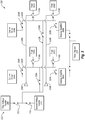
- FIG. 2 is a block diagram of a pixel continuity testing system (testing system) 200 which may be integrated into the LCOS system of Figure 1 .
- the testing system 200 may perform a continuity test on pixels 202A-202D (generally, pixel 202 or pixels 202).
- a continuity test may detect, for example, pixels 202 that may be damaged and/or nonfunctional.
- the testing system 200 depicted in Figure 2 includes four pixels 202: a first pixel 202A, a second pixel 202B, a third pixel 202C, and a fourth pixel 202D.
- the testing system 200 in Figure 2 represents a simplified version of the testing system 200.
- the principles disclosed with respect to the testing system 200 may be scaled to be integrated into a testing system including more than four pixels 202.
- the pixels 202 may be substantially similar to and/or correspond to the pixels 126 described with respect to Figure 1 and may be essentially identical to one another.
- the pixels 202 may be organized into columns and rows with a yank wire 236, row wires 228A and 228B, and column wires 222A and 222B.
- the row wires 228A and 228B are substantially similar to the row wires 128 and the column wires 222A and 222B are substantially similar to the column wires 130 discussed with reference to Figure 1 .
- the first pixel 202A and the third pixel 202C may be selectively coupled to a first column wire 222A and the second pixel 202B and the fourth pixel 202D may be selectively coupled to a second column wire 222B.
- Each pixel 202 is selectively coupled to one of the column wires 222A or 222B through operation of corresponding pixel switches 218A-218D.
- the pixel switches 218A-218D may be operated by one or more row enable amplifiers 230A and 230B positioned at an end of each of the row wires 228A and 228B.
- the row enable amplifiers 230A and 230B are operational amplifiers. However, this depiction is not meant to be limiting.
- the row enable amplifiers 230A and 230B may be switches or some other suitable structure, for instance.
- the first pixel 202A may be coupled to the first column wire 222A by a first row enable amplifier 230A communicating a signal to close a first pixel switch 218A.
- the fourth pixel 202D may be isolated from the second column wire 222B by a second row enable amplifier 230B communicating a signal to open a fourth pixel switch 218D.
- the second pixel 202B and the third pixel 202C may be selectively coupled to the first column wire 222A and the second column wire 222B, respectively.
- the term "open” refers to a state of a switch or amplifier in which the flow of electricity stops.
- the term “closed” refers to a state of a switch or amplifier in which the flow of electricity is enabled.
- the yank wire 236 selectively couples the first column wire 222A and the second column wire 222B to a yank structure 232. More specifically, operation of a first column yank switch 226A selectively couples the yank structure 232 to the first column wire 222A and a second column yank switch 226B selectively couples the yank structure 232 to the second column wire 222B. Some additional details of the yank structure 232 are provided below.
- the testing system 200 may also include column drivers 204A and 204B which may be similar to and/or correspond to the column drivers 112 described with respect to Figure 1 . That is, the column drivers 204A and 204B may write images to one or more of the pixels 202.
- a first column driver 204A may be selectively coupled to the first column wire 222A via a first column driver switch 224A and a second column driver 204B may be selectively coupled to the second column wire 222B via a second column driver switch 224B. Accordingly, the column drivers 204A and 204B may be isolated from the column wires 222A and 222B by opening the column driver switches 224A and 224B.
- the testing system 200 may also include one or more sensing amplifiers 300A and 300B (generally, sensing amplifier 300 or sensing amplifiers 300).
- a first sensing amplifier 300A may be selectively coupled to the first column wire 222A via a first sensing amplifier switch 220A.
- the first sensing amplifier 300A may be isolated from the first column wire 222A by opening a first sensing amplifier switch 220A.
- the testing system 200 may include a second sensing amplifier 300B that may be selectively coupled to the second column wire 222B via a second sensing amplifier switch 220B.
- the second sensing amplifier 300B may be isolated from the second column wire 222B by opening a second sensing amplifier switch 220B.
- the first sensing amplifier 300A may also be selectively coupled to the second column wire 222B.
- the testing system 200 may include an additional sensing amplifier switch (not shown) that isolates the first sensing amplifier 300A from the second column wire 222B.
- FIG 3 is a block diagram of an example sensing amplifier 300 that may be implemented in the testing system 200 depicted in Figure 2 .
- the sensing amplifier 300 may include the sensing amplifier switch 220, which may selectively couple the sensing amplifier 300 to one of the column wires 222A or 222B.
- the sensing amplifier switch 220 is depicted in both Figures 2 and 3 .
- the sensing amplifier 300 may generally include a differential amplifier sensing circuit 302, a sample switch 304, and one or more inverting amplifiers 310.
- the sensing circuit 302 obtains a voltage at an input 308 when the sample switch 304 in a feedback leg is closed.
- the sensing circuit 302 amplifies and charges the voltage to trigger the inverting amplifiers 310.
- the sensing circuit 302 becomes a comparator circuit, thereby resetting the sensing circuit 302.
- the sensing amplifier 300 may be selectively coupled to one of the column wires 222A or 222B via a sensing amplifier switch 220A or 220B. With the sensing amplifier switch 220A or 220B closed, the column wire 222A or 222B is electrically coupled to the input 308 of the sensing circuit 302. When the sample switch 304 closes, the sensing amplifier 300 can sense a voltage on the column wire 222A or 222B.
- the sensing amplifier 300 may include a trigger (not shown) including a programmable threshold.
- the threshold of the trigger may accommodate for process, voltage, and temperature (PVT) variation. Additionally or alternatively, in some embodiments, the capture time may be programmable.
- the yank structure 232 may include a yank down switch 210 and a yank up switch 212 that selectively couple the column wires 222A and 222B to a second voltage source 214 and a first voltage source 206, respectively.
- the yank down switch 210 and a first column yank switch 226A may be closed.
- the rest of the testing system 200 may be isolated from the second voltage source 214.
- the second column yank switch 226B, the first pixel switch 218A, the third pixel switch 218C, the first sensing amplifier switch 220A, and the first column driver switch 224A may be open.
- the yank down switch 210 and the second column yank switch 226B may be closed.
- the rest of the testing system 200 may be isolated from the second voltage source 214.
- the first column yank switch 226A, the second pixel switch 218B, the fourth pixel switch 218D, the second sensing amplifier switch 220B, and the second column driver switch 224B may be open.
- the column wires 222A and 222B may be selectively coupled to the first voltage source.
- the first voltage source 206 may be coupled to the first column wire 222A by closing the yank up switch 212 and the first column yank switch 226A.
- the first voltage source 206 may be coupled to the second column wire 222B by closing the yank up switch 212 and the second column yank switch 226B.
- the rest of the testing system 200 may be isolated from the first voltage source 206.
- the first voltage source 206 may be greater than the second voltage source 214.
- the first voltage source 206 may be approximately equal to 10 V and the second voltage source 214 may be an electrical ground.
- the testing system 200 includes the yank structure 232 and the column yank switches 226A and 226B to sequentially couple the column wires 222A or 222B and the pixels 202 to the first voltage source 206 and the second voltage source 214.
- a resultant voltage (not shown) may be produced on the column wires 222A and 222B.
- the resultant voltage may be sensed by the sensing amplifier 300.
- the resultant voltage may be an indication of continuity of the pixels 202.
- a pixel continuity test may include sensing and analyzing the resultant voltage for each of the pixels 202.
- the resultant voltages for each of the pixels 202 may be sensed by the sensing amplifiers 208A and 208B.
- the testing system 200 may include a scan register 216.
- the scan register 216 may be selectively coupled to the first sensing amplifier 208A and the second sensing amplifier 208B. When coupled to the first sensing amplifier 208A or the second sensing amplifier 208B, the scan register 216 may record or store the resultant voltages sensed by the sensing amplifiers 208A and 208B. In alternative embodiments, the resultant voltages may be fed to a remote storage component.
- Figure 4 is an example signal diagram 400 depicting an example sequence of the testing system 200 depicted in Figure 2 .
- the signal diagram 400 depicts a sequence to sense a resultant voltage of the first pixel 202A.
- the first pixel 202A is tested; however, through a similar sequence any of the pixels 202 may be tested.
- FIG 4 there are five signal lines representing the states of various switches in the testing system 200 depicted in Figure 2 and the sensing amplifier 300 depicted in Figure 3 . Also, in Figure 4 there are thirteen dashed, vertical lines 402-426 representing time included in the example sequence. The state of the switch is closed when the signal line is high and the state of the switch is open when the signal line is low. Specifically, with combined reference to Figures 2-4 , a first signal 428 represents the state of the yank down switch 210. A second signal 430 represents the state of the sample switch 304. A third signal 432 represents the state of the first sensing amplifier switch 220A. A fourth signal 434 represents the state of the first pixel switch 218A. A fifth signal 436 represents the state of the yank up switch 212.
- the first column yank switch 226A remains closed and the state of the first pixel switch 218A is controlled by the row enable amplifier 230A.
- the remaining switches e.g., 224B, 218B, 218D, 220B, 226B, 218C, and 224A depicted in Figure 2 remain open during the example sequence.
- the yank down switch 210 is closed, the sample switch 304 is open, the first sensing amplifier switch 220A is open, the first pixel switch 218A is open, and the yank up switch 212 is open.
- the first sensing amplifier switch 220A closes.
- the first column wire 222A and the first sensing amplifier 300A are coupled to the second voltage source 214.
- the second voltage source 214 is an electrical ground
- the first column wire 222A is grounded.
- a series of switches change state that results in an image being written to the first pixel 202A.
- the yank down switch opens.
- the first sensing amplifier switch 220A opens.
- the first pixel switch 218A closes.
- the yank up switch closes. In this configuration, a voltage from the first voltage source 206 is applied through the yank up switch 212 to the first pixel 202A. The voltage applied to the first pixel 202A writes the image to the first pixel 202A.
- the first voltage source 206 may be coupled to the second pixel 202B as well.
- the image written to the first pixel 202A may be identical to the image written to the second pixel 202B.
- a series of switches change state that isolate the first pixel 202A, and thereby store charge in the first pixel 202A.
- the first pixel switch 218A opens.
- the yank up switch 212 opens. In this configuration, the first pixel 202A is isolated from the first column wire 222A.
- a series of switches change state that couple the first column wire 222A to the second voltage source 214.
- the yank down switch 210 closes.
- the first sensing amplifier switch 220A closes.
- the first column wire 222A and the first sensing amplifier 208A are coupled to the second voltage source 214.
- the second voltage source 214 is an electrical ground, in this configuration the first column wire 222A is discharged.
- the yank down switch 210 opens.
- the sample switch 304 closes such that the first sensing amplifier 208A may sense the voltage on the first column wire 222A.
- the first pixel switch 218A closes, coupling the first pixel 202A to the first column wire 222A.
- the charge stored in the first pixel 202A is shared with the first column wire 222A.
- the first sensing amplifier 208A can sense a resultant voltage on the first column wire 222A.
- the pixels 202 may include a pixel capacitance, which may be different from a column wire capacitance. A difference in capacitance may result in the charge sharing discussed above.
- FIG 5 is a flowchart of an example pixel continuity testing method (method) 500.
- the method 500 can be implemented with the testing system 200 of Figure 2 in some embodiments.
- One skilled in the art will appreciate that, for this and other processes and methods disclosed herein, the functions performed in the processes and methods may be implemented in differing order.
- the outlined steps and operations are only provided as examples, and some of the steps and operations may be optional, combined into fewer steps and operations, or expanded into additional steps and operations without detracting from the disclosed embodiments.
- the method 500 may begin at 502 by writing a first voltage to a pixel.
- writing the first voltage to the pixel may include closing a yank up switch coupled to a first voltage source.
- the method 500 may include isolating the pixel.
- Isolating the pixel may include opening a pixel switch, which may be controlled by an enable amplifier.
- the first voltage written to the pixel may be stored as a charge in the pixel.
- the method 500 may include discharging a wire that is selectively coupled to the pixel. Discharging the wire may include closing a yank down switch coupled to an electrical ground.
- the wire may be a column wire that electrically couples to the pixel and a second pixel. In this and other embodiments, the wire may be selectively coupled to the pixel and the second pixel via the pixel switch and a second pixel switch, respectively.
- the method 500 may include enabling a sensing amplifier that senses voltage on the wire.
- the sensing amplifier may include a sensing circuit that includes a trigger with a threshold.
- the threshold for the trigger of the sensing amplifier may be programmed to compensate for process, voltage, and temperature (PVT) variation.
- the sensing circuit may include a capture time that holds the voltage sensed by the sensing amplifier. In some of these embodiments, the capture time may be programmed.
- the method 500 may include electrically connecting the pixel to the wire and connecting the pixel to the wire may include closing the pixel switch such that the charge stored in the pixel may be shared with the wire.
- the charge sharing may be a result of differences between a pixel capacitance of the pixel and a wire capacitance of the wire. For example, in some embodiments, the pixel capacitance is less than the wire capacitance.
- the method 500 may include sensing a resultant voltage on the wire.
- the resultant voltage may include the charge shared between the pixel and the wire.
- the resultant voltage may indicate proper continuity of the pixel.
- one sensing amplifier may be selectively coupled to multiple columns and/or multiple pixels in some sequence. This may enable the one sensing amplifier to sense the resultant voltage for the multiple pixels.
- the method 500 may be performed for each of the pixels individually.
- a LCOS IC may include a system such as the testing system 200 of Figure 2 that implements the method 500.
- the LCOS IC may record or store the resultant voltage in a scan register, for instance.
- the resultant voltage may be fed off the LCOS IC and/or stored remotely.
Landscapes
- Physics & Mathematics (AREA)
- Engineering & Computer Science (AREA)
- General Physics & Mathematics (AREA)
- Nonlinear Science (AREA)
- Computer Networks & Wireless Communication (AREA)
- Theoretical Computer Science (AREA)
- Computer Hardware Design (AREA)
- Mathematical Physics (AREA)
- Crystallography & Structural Chemistry (AREA)
- Optics & Photonics (AREA)
- Chemical & Material Sciences (AREA)
- Microelectronics & Electronic Packaging (AREA)
- Testing Of Short-Circuits, Discontinuities, Leakage, Or Incorrect Line Connections (AREA)
- Liquid Crystal Display Device Control (AREA)
- Control Of Indicators Other Than Cathode Ray Tubes (AREA)
- Liquid Crystal (AREA)
- Testing Of Individual Semiconductor Devices (AREA)
Description
- Embodiments described herein relate generally to optical switches. More particularly, example embodiments relate to liquid crystal on silicon integrated circuits (LCOS ICs) that may be included into optical switches.
- Signal-carrying light may be multiplexed onto an optical fiber to increase the capacity of the optical fiber and/or enable bidirectional transmission. Optical switches are generally used to multiplex, de-multiplex, or dynamically route a particular channel of the signal-carrying light. One type of optical switch is a wavelength selector switch (WSS) which routes the particular channel based on the wavelength of the particular channel.
- In some WSS, liquid crystal on silicon (LCOS) technology is used to create a display engine that deflects a wavelength of the particular channel. In LCOS technology, liquid crystals may be applied to a surface of a silicon chip. The silicon chip may be coated with a reflective layer. For example, the reflective layer may include an aluminized layer. Additionally, in LCOS technology, the display engine may include multiple pixels. Through introduction and alteration of electrical voltage applied to the pixels, the pixels create an electrically controlled grating that routes the particular channel in a deflected direction.
-
US 2004/135596 A1 describes a method of electrically inspecting display devices, which is capable of inspecting whether a signal is normally input to the pixels and whether an electric charge is normally held by the holding capacitors without using the video signal line as a passage for reading the electric charge and without separately providing an inspection-dedicated circuit. - This background is only provided to illustrate one exemplary technology area where some embodiments described herein may be practiced
- Embodiments described herein relate generally to optical switches. More particularly, example embodiments relate to liquid crystal on silicon integrated circuits (LCOS ICs) that may be included in optical switches.
- One aspect relates to a continuity testing method of a pixel in a LCOS IC according to appended claim 9. The method includes writing a first voltage to a pixel. The pixel is isolated and a wire that is selectively coupled to the pixel is discharged. The method also includes enabling a sensing amplifier configured to sense voltage on the wire. The pixel is electrically connected to the wire and a resultant voltage on the wire is sensed.
- Another aspect relates to a pixel continuity testing system of a LCOS IC according to appended claim 1. The testing system includes a first pixel, a first wire, a yank structure, and a sensing amplifier. The first wire is selectively coupled to the first pixel via a first pixel switch. The yank structure includes a yank up switch configured to couple the first pixel to a first voltage source and a yank down switch configured to couple the first wire to a second voltage source. The sensing amplifier is configured to be selectively coupled to the first wire via a sensing amplifier switch and configured to sense a first resultant voltage on the first wire following the first pixel being coupled to the first voltage source. Thus, embodiments concern a LCOS IC. The LCOS IC includes multiple pixels, a yank structure, and multiple sensing amplifiers. The pixels are arranged in rows of pixels and in columns of pixels, the columns of pixels are electrically coupled via column wires. The yank structure includes a yank up switch configured to couple the columns of pixels to a first voltage source and a yank down switch configured to couple the columns of pixels to an electrical ground. Each of the sensing amplifiers is configured to sense a resultant voltage on at least one of the column wires.
- This Summary is provided to introduce a selection of concepts in a simplified form that are further described below in the Detailed Description.
- Additional features and advantages of the invention will be set forth in the description, which follows, and in part will be obvious from the description, or may be learned by the practice of the invention. The features and advantages of the invention may be realized and obtained by means of the instruments and combinations particularly pointed out in the appended claims. These and other features of the present invention will become more fully apparent from the following description and appended claims, or may be learned by the practice of the invention as set forth hereinafter.
- To further clarify the above and other advantages and features of the present invention, a more particular description of the invention will be rendered by reference to specific embodiments thereof, which are illustrated in the appended drawings. It is appreciated that these drawings depict only typical embodiments of the invention and are, therefore, not to be considered limiting of its scope. The invention will be described and explained with additional specificity and detail through the use of the accompanying drawings in which:
-
Figure 1 is a block diagram of an example liquid crystal on silicon (LCOS) system in which the embodiments disclosed herein may be implemented; -
Figure 2 is a block diagram of a pixel continuity testing system (testing system) which may be integrated into the LCOS system ofFigure 1 ; -
Figure 3 is a block diagram of an example sensing amplifier that may be implemented in the testing system ofFigure 2 ; -
Figure 4 is an example signal diagram depicting an example sequence of the testing system ofFigure 2 ; and -
Figure 5 is a flowchart of an example pixel continuity testing method that may be implemented in the LCOS system ofFigure 1 . - Embodiments described herein relate generally to optical switches. More particularly, example embodiments relate to liquid crystal on silicon integrated circuits (LCOS ICs) that may be included in optical switches. An example embodiment includes a pixel continuity testing system for a LCOS IC. The testing system includes a wire that is selectively coupled to a pixel via a pixel switch. The wire is also selectively coupled to a sensing amplifier via a sensing amplifier switch. A yank up switch couples the pixel to a first voltage. The yank down switch couples the wire to a second voltage. The sensing amplifier senses a resultant voltage on the first wire when the wire is coupled to the first pixel. Some additional example embodiments of the present invention will be explained with reference to the accompanying drawings.
-
Figure 1 is a block diagram of an example liquid crystal on silicon (LCOS)system 100 in which the embodiments disclosed herein may be implemented. Generally, theLCOS system 100 writes images used to select wavelength or channels of optical signal-carrying light (optical signals). The LCOSsystem 100 can include a driver chip such as a field-programmable gate array (FPGA) 102 that controls the liquid crystal on silicon integrated circuit (LCOS IC) 124. To control the LCOS IC 124, theFPGA 102 communicates commands, synchronization signals, digital data, varying analog and/or digital signals, or some combination thereof. Additionally, theFPGA 102 may receive various analog and/or digital data signals, output synchronization signals, etc. from the LCOS IC 124. - The FPGA 102 is an integrated circuit (IC) with logic blocks, which may be configured to perform one or more control functions of the LCOS IC 124. The FPGA 102 may be configured and/or programmed after the
LCOS system 100 is delivered to a user or following manufacturing of theFPGA 102. In some alternative embodiments the driver chip may include an application-specific integrated circuit (ASIC) or another suitable driver chip having substantially equivalent capabilities of theFPGA 102. - The FPGA 102 may include a
digital port 142 which may communicate with ademultiplexing module 116 included in the LCOS IC 124. An example of thedigital port 142 may include a low-voltage differential signal (LVDS) pair. TheFPGA 102 may communicate digital data through thedigital port 142 to thedemultiplexing module 116. InFigure 1 ,arrow 132 represents the communication of digital data to thedemultiplexing module 116. Digital data may include, but is not limited to, a digital clock signal that may be used as a synchronization signal and digital image data for one ormore pixels 126A-1261 (generally,pixel 126 or pixels 126) included in theLCOS IC 124. The digital image data includes a digital representation of an image theLCOS IC 124 displays. The digital image data may be formatted as 6 bit per pixel, 7 bit per pixel, or 8 bit per pixel, for example. The digital data, or some portion thereof, may be communicated to one ormore column drivers 112A-112C (generally, column driver 112 or column drivers 112) which may then be communicated to thepixels 126. - Some embodiments of the
FPGA 102 may include multipledigital ports 142 and/or theLCOS IC 124 may includemultiple demultiplexing modules 116. In embodiments in which theFPGA 102 includes multipledigital ports 142, theFPGA 102 may communicate a specific or a set amount of digital data through each of thedigital ports 142 in parallel. For example, in some embodiments, theFPGA 102 includes thirty-twodigital ports 142. Each of the thirty-twodigital ports 142 may communicate digital image data for a bank ofpixels 126, including sixty columns ofpixels 126. - The
FPGA 102 may also include acommand port 144 that communicates commands to acommand decoder 108. InFigure 1 ,arrow 136 represents the communication of commands to thecommand decoder 108. The commands may include one or more actions and/or functions for theLCOS IC 124 to perform. For example, a command may include timing of operations to write a row of thepixels 126. A timing command may be controlled by theFPGA 102 via thecommand port 144. Additionally or alternatively, a command may include a digital clock signal that may be used as a synchronization signal. In some embodiments, theFPGA 102 may includemultiple command ports 144. - The
command decoder 108 and thecommand port 144 may also communicate additional signals. InFigure 1 , double-endedarrow 134 represents the communication of additional signals between thecommand port 144 and thecommand decoder 108. For example, the additional signals may include, but are not limited to, an auxiliary digital data signal, a reset signal, data out signals from theLCOS IC 124, and output clock signals from theLCOS IC 124. The reset signal and the auxiliary digital data signal may include a digital clock signal as a synchronization signal. The data out signals and the output clock signals may communicate information regarding synchronization and operational status of theLCOS IC 124 to theFPGA 102. - The
FPGA 102 may also include ananalog module 104 that communicates analog signals with anLCOS analog module 118. InFigure 1 , the double-endedarrow 146 represents the communication between theanalog module 104 and theLCOS analog module 118. TheFPGA 102 may also communicate a digital ramp signal to a digital to analog converter (DAC) 106. InFigure 1 ,arrow 138 represents the communication of the digital ramp signal to theDAC 106. TheDAC 106 receives the digital ramp signal and outputs an analog ramp signal related to the digital ramp signal. The digital ramp signal is a binary number that represents and is proportional to an analog voltage of the analog ramp signal output from theDAC 106. - In some embodiment, the digital ramp signal includes a series of binary numbers that are converted to a monotonically varying voltage which ramps from an initial voltage to a final voltage. The term "ramp" refers to the behavior of incrementally varying at a defined rate. That is, in some embodiments, an initial binary number of the digital ramp signal is converted to an initial voltage which may be as high as about 12 volts (V). The digital ramp signal may subsequently include binary numbers resulting in an analog ramp signal that monotonically steps down to a final voltage. Alternatively, an initial binary number of the digital ramp signal can be converted to an initial voltage which may be as low as 0 V. The digital ramp signal may subsequently include binary numbers that result in voltages that monotonically step up to a final voltage. In some embodiments, each step may be a predetermined time interval during which the digital ramp signal includes a binary number that results in a predetermined change in voltage. Additionally, the digital ramp signal may vary according to a gamma curve, which can correct for nonlinear optical response of LCOS material.
- The digital ramp signal is not limited to the series of binary numbers that result in the monotonically ramping voltage. The digital ramp signal can include a series of binary numbers that result in multiple patterns or progressions of voltages. For example, the digital ramp signal can include binary numbers that result in a set of increasing voltages and then a set of decreasing voltages, vice versa, or some other suitable pattern resulting in voltages covering the range of voltages to drive the
pixels 126 of the LCOS IC 124A. As stated above, theDAC 106 converts the digital ramp signal to an analog ramp signal representative of the binary number included in the digital ramp signal. Accordingly, the analog ramp signal is an analog representation of the digital ramp signal. The analog ramp signal may exhibit incrementally varying behavior equivalent or related to the digital ramp signal. Thus, in some embodiments, the analog ramp signal monotonously varies from the initial voltage to the final voltage, supplying a varying voltage signal to thepixels 126. More specifically, the analog ramp signal supplies target voltages to thepixels 126. The target voltages are defined voltages within the inclusive range of the initial voltage to the final voltage of the analog ramp signal. The LCOS IC 124A operates, at least partially, through driving the target voltages to thepixels 126. - A brightness of a
pixel 126 may be determined by the magnitude of a target voltage supplied to thepixel 126. Thus, the brightness of thepixel 126 is controlled by driving the analog ramp signal during the time in which the target voltage of the analog ramp signal is equal to the voltage corresponding to a desired brightness.Pixels 126 may include multiple levels of brightness. For example, in some embodiments thepixel 126 can be programmed to display 256 or more levels of brightness. The process of supplying thepixels 126 with target voltages may be referred to as "writing an image." - Additionally, the analog ramp signal may monotonically vary from the initial voltage to the final voltage once per writing cycle of the
pixels 126. The initial voltage and the final voltage may periodically change, interchange, or turn around. That is, in a first writing cycle, the final voltage may be greater than the initial voltage. In a second writing cycle, the initial voltage may be greater than the final voltage. In a third cycle, the final voltage may again be greater than the initial voltage. The initial voltage and the final voltage may continue to change in this pattern. - To determine when to supply the analog ramp signal to the
pixels 126, theFPGA 102 may also communicate a ramp counter enable signal to aramp counter 114 included in theLCOS IC 124. InFigure 1 ,arrow 140 represents the communication of the ramp counter enable signal to theramp counter 114. Generally, theramp counter 114 receives the ramp counter enable signal from theFPGA 102, which enables or turns on theramp counter 114. Once enabled, theramp counter 114 counts or tracks the number of predetermined time intervals of the digital ramp signal that have occurred since receiving the ramp counter enable signal. The number of predetermined time intervals of the digital ramp signal may be equivalent and/or related to the number of predetermined time intervals of the analog ramp signal. More specifically, in some embodiments, the digital ramp signal may include a ramp clock signal. The ramp clock signal may act as a synchronization signal. Theramp counter 114 may track and/or count the number of predetermined time intervals included in the ramp clock signal following the reception of the ramp counter enable signal. Theramp counter 114 may output or otherwise make available a ramp step signal indicating the number of predetermined time intervals. - The
ramp counter 114 may be coupled to the column drivers 112. Theramp counter 114 may communicate the ramp step signal to the column drivers 112. Thus, theramp counter 114 and the ramp step signal may be used to determine the voltage of the analog ramp signal at a specific time. That is, the voltage of the analog ramp signal may be calculated if the initial voltage resulting from an initial binary number of the digital ramp signal, the predetermined voltage change per predetermined time interval, and the ramp step signal are known. - Referring back to the
DAC 106, the analog ramp signal exiting theDAC 106, which is indicated by theline 148, enters anexternal buffer 150. Theexternal buffer 150 may buffer theDAC 106 and/or theFPGA 102 from theLCOS IC 124. From theexternal buffer 150, the analog ramp signal enters theLCOS IC 124 and supplies the column drivers 112, which then supplies thepixels 126 or some subset thereof included in anarray core 120. - Each of the
pixels 126 may include a NMOS/PMOS complementary switch, a metal insulator-metal (MIM) capacitor, and a piece of top-layer metal. The complementary switch may enable linear transfer of voltage supplied by the column drivers 112 to enter thepixel 126. The MIM capacitor may be included to provide enough capacitive storage to limit charge leakage during a field time. In the depicted embodiment, thearray core 120 includes ninepixels 126. However, this depiction is not limiting. The ellipses are included to illustrate that thearray core 120 may include more than ninepixels 126. In some embodiments, thearray core 120 may be separated into banks of columns which banks of columns may be coupled to one of the digital port 142 (described above). - In this and other embodiments, the
array core 120 includes thepixels 126 that may be organized into columns and rows. Thepixels 126 in each row may be electrically coupled to arow decode 110 via arow wire 128A-128C (generally, row wire 128 or row wires 128). The row decode 110 may receive commands from thecommand decoder 108. Specifically, the row decode 110 may receive commands related to activation of thepixels 126 in a row. The row decode 110 may then communicate the command related to activation through a row enableamplifier 122A-122C (generally, row enable amplifier 122 or row enable amplifiers 122), along one of the row wires 128 to thepixels 126 in the row. The activation signal enables or triggers the receiving pixels (i.e., thepixels 126 in the row coupled to the row enable amplifier 122) to become activated such that thepixels 126 may receive one or more signals supplied by one of the column drivers 112. - In some embodiments, the
pixels 126 may be activated row by row. That is, the first row enableamplifier 122A communicates the activation signal to thefirst pixel 126A, thesecond pixel 126B, and thethird pixel 126C through thefirst row wire 128A. After thefirst pixel 126A, thesecond pixel 126B, and thethird pixel 126C are written, the second row enableamplifier 122B then communicates the activation signal to thefourth pixel 126D, thefifth pixel 126E, and thesixth pixel 126F through thesecond row wire 128B. Thepixels 126 in each column may be electrically coupled to one of the column drivers 112 via one ormore column wires 130A-130C (generally, column wire 130 or column wires 130). Each of the column drivers 112 supplies one or more signals to thepixels 126 in a column via the column wire 130. -
Figure 2 is a block diagram of a pixel continuity testing system (testing system) 200 which may be integrated into the LCOS system ofFigure 1 . Generally, thetesting system 200 may perform a continuity test onpixels 202A-202D (generally, pixel 202 or pixels 202). A continuity test may detect, for example, pixels 202 that may be damaged and/or nonfunctional. Thetesting system 200 depicted inFigure 2 includes four pixels 202: afirst pixel 202A, asecond pixel 202B, athird pixel 202C, and afourth pixel 202D. However, thetesting system 200 inFigure 2 represents a simplified version of thetesting system 200. The principles disclosed with respect to thetesting system 200 may be scaled to be integrated into a testing system including more than four pixels 202. - In general, the pixels 202 may be substantially similar to and/or correspond to the
pixels 126 described with respect toFigure 1 and may be essentially identical to one another. The pixels 202 may be organized into columns and rows with a yankwire 236,row wires column wires row wires column wires Figure 1 . Thefirst pixel 202A and thethird pixel 202C may be selectively coupled to afirst column wire 222A and thesecond pixel 202B and thefourth pixel 202D may be selectively coupled to asecond column wire 222B. Each pixel 202 is selectively coupled to one of thecolumn wires amplifiers row wires Figure 2 , the row enableamplifiers amplifiers - For example, the
first pixel 202A may be coupled to thefirst column wire 222A by a first row enableamplifier 230A communicating a signal to close afirst pixel switch 218A. Likewise, thefourth pixel 202D may be isolated from thesecond column wire 222B by a second row enableamplifier 230B communicating a signal to open afourth pixel switch 218D. In a similar fashion, thesecond pixel 202B and thethird pixel 202C may be selectively coupled to thefirst column wire 222A and thesecond column wire 222B, respectively. As used herein the term "open" refers to a state of a switch or amplifier in which the flow of electricity stops. Conversely, the term "closed" refers to a state of a switch or amplifier in which the flow of electricity is enabled. - The yank
wire 236 selectively couples thefirst column wire 222A and thesecond column wire 222B to a yankstructure 232. More specifically, operation of a first column yankswitch 226A selectively couples the yankstructure 232 to thefirst column wire 222A and a second column yankswitch 226B selectively couples the yankstructure 232 to thesecond column wire 222B. Some additional details of the yankstructure 232 are provided below. - In some embodiments, the
testing system 200 may also includecolumn drivers Figure 1 . That is, thecolumn drivers first column driver 204A may be selectively coupled to thefirst column wire 222A via a firstcolumn driver switch 224A and asecond column driver 204B may be selectively coupled to thesecond column wire 222B via a secondcolumn driver switch 224B. Accordingly, thecolumn drivers column wires column driver switches - The
testing system 200 may also include one ormore sensing amplifiers amplifier 300 or sensing amplifiers 300). Afirst sensing amplifier 300A may be selectively coupled to thefirst column wire 222A via a firstsensing amplifier switch 220A. For example, thefirst sensing amplifier 300A may be isolated from thefirst column wire 222A by opening a firstsensing amplifier switch 220A. - Additionally, the
testing system 200 may include asecond sensing amplifier 300B that may be selectively coupled to thesecond column wire 222B via a secondsensing amplifier switch 220B. For example, thesecond sensing amplifier 300B may be isolated from thesecond column wire 222B by opening a secondsensing amplifier switch 220B. In some embodiments, instead of including thesecond sensing amplifier 300B, thefirst sensing amplifier 300A may also be selectively coupled to thesecond column wire 222B. In these and other embodiments, thetesting system 200 may include an additional sensing amplifier switch (not shown) that isolates thefirst sensing amplifier 300A from thesecond column wire 222B. -
Figure 3 is a block diagram of anexample sensing amplifier 300 that may be implemented in thetesting system 200 depicted inFigure 2 . With combined reference toFigures 2 and3 , thesensing amplifier 300 may include thesensing amplifier switch 220, which may selectively couple thesensing amplifier 300 to one of thecolumn wires sensing amplifier switch 220 is depicted in bothFigures 2 and3 . - Referring to
Figure 3 , thesensing amplifier 300 may generally include a differentialamplifier sensing circuit 302, asample switch 304, and one ormore inverting amplifiers 310. Generally, thesensing circuit 302 obtains a voltage at aninput 308 when thesample switch 304 in a feedback leg is closed. Thesensing circuit 302 amplifies and charges the voltage to trigger the invertingamplifiers 310. When thesample switch 304 is open, thesensing circuit 302 becomes a comparator circuit, thereby resetting thesensing circuit 302. - With combined reference to
Figures 2 and3 , thesensing amplifier 300 may be selectively coupled to one of thecolumn wires sensing amplifier switch sensing amplifier switch column wire input 308 of thesensing circuit 302. When thesample switch 304 closes, thesensing amplifier 300 can sense a voltage on thecolumn wire - In some embodiments, the
sensing amplifier 300 may include a trigger (not shown) including a programmable threshold. The threshold of the trigger may accommodate for process, voltage, and temperature (PVT) variation. Additionally or alternatively, in some embodiments, the capture time may be programmable. - Referring back to
Figure 2 , the yankstructure 232 may include a yank downswitch 210 and a yank upswitch 212 that selectively couple thecolumn wires second voltage source 214 and afirst voltage source 206, respectively. To couple thefirst column wire 222A to thesecond voltage source 214, the yank downswitch 210 and a first column yankswitch 226A may be closed. When thefirst column wire 222A is coupled to thesecond voltage source 214, the rest of thetesting system 200 may be isolated from thesecond voltage source 214. Specifically, the second column yankswitch 226B, thefirst pixel switch 218A, thethird pixel switch 218C, the firstsensing amplifier switch 220A, and the firstcolumn driver switch 224A may be open. - Likewise to couple the
second column wire 222B to thesecond voltage source 214, the yank downswitch 210 and the second column yankswitch 226B may be closed. When thesecond column wire 222B is coupled to thesecond voltage source 214, the rest of thetesting system 200 may be isolated from thesecond voltage source 214. Additionally, the first column yankswitch 226A, thesecond pixel switch 218B, thefourth pixel switch 218D, the secondsensing amplifier switch 220B, and the secondcolumn driver switch 224B may be open. - In a similar fashion, through operation of the yank up
switch 212 and the first and second column yankswitches column wires first voltage source 206 may be coupled to thefirst column wire 222A by closing the yank upswitch 212 and the first column yankswitch 226A. Likewise, thefirst voltage source 206 may be coupled to thesecond column wire 222B by closing the yank upswitch 212 and the second column yankswitch 226B. In either configuration, e.g., thefirst voltage source 206 being coupled to the first column wire orsecond column wire testing system 200 may be isolated from thefirst voltage source 206. - In some embodiments, the
first voltage source 206 may be greater than thesecond voltage source 214. For example, in some embodiments, thefirst voltage source 206 may be approximately equal to 10 V and thesecond voltage source 214 may be an electrical ground. - The
testing system 200 includes the yankstructure 232 and the column yankswitches column wires first voltage source 206 and thesecond voltage source 214. By sequentially coupling thecolumn wires first voltage source 206 and thesecond voltage source 214, a resultant voltage (not shown) may be produced on thecolumn wires sensing amplifier 300. The resultant voltage may be an indication of continuity of the pixels 202. A pixel continuity test may include sensing and analyzing the resultant voltage for each of the pixels 202. In thetesting system 200, by changing the states of the switches (e.g., 212, 210, 226A, 226B, 218A-218D, 220A, 220B, and 224A-224D) described above in a particular sequence, the resultant voltages for each of the pixels 202 may be sensed by the sensing amplifiers 208A and 208B. - Additionally, in some embodiments, the
testing system 200 may include ascan register 216. Thescan register 216 may be selectively coupled to the first sensing amplifier 208A and the second sensing amplifier 208B. When coupled to the first sensing amplifier 208A or the second sensing amplifier 208B, thescan register 216 may record or store the resultant voltages sensed by the sensing amplifiers 208A and 208B. In alternative embodiments, the resultant voltages may be fed to a remote storage component. -
Figure 4 is an example signal diagram 400 depicting an example sequence of thetesting system 200 depicted inFigure 2 . With combined reference toFigures 2 and4 , the signal diagram 400 depicts a sequence to sense a resultant voltage of thefirst pixel 202A. In the depicted embodiment, thefirst pixel 202A is tested; however, through a similar sequence any of the pixels 202 may be tested. - In
Figure 4 , there are five signal lines representing the states of various switches in thetesting system 200 depicted inFigure 2 and thesensing amplifier 300 depicted inFigure 3 . Also, inFigure 4 there are thirteen dashed, vertical lines 402-426 representing time included in the example sequence. The state of the switch is closed when the signal line is high and the state of the switch is open when the signal line is low. Specifically, with combined reference toFigures 2-4 , afirst signal 428 represents the state of the yank downswitch 210. Asecond signal 430 represents the state of thesample switch 304. Athird signal 432 represents the state of the firstsensing amplifier switch 220A. Afourth signal 434 represents the state of thefirst pixel switch 218A. Afifth signal 436 represents the state of the yank upswitch 212. - Throughout the example sequence, the first column yank
switch 226A remains closed and the state of thefirst pixel switch 218A is controlled by the row enableamplifier 230A. The remaining switches (e.g., 224B, 218B, 218D, 220B, 226B, 218C, and 224A) depicted inFigure 2 remain open during the example sequence. - Beginning at a
first time 426, the yank downswitch 210 is closed, thesample switch 304 is open, the firstsensing amplifier switch 220A is open, thefirst pixel switch 218A is open, and the yank upswitch 212 is open. - At a
second time 424, the firstsensing amplifier switch 220A closes. Thus, attime 424 thefirst column wire 222A and thefirst sensing amplifier 300A are coupled to thesecond voltage source 214. In embodiments in which thesecond voltage source 214 is an electrical ground, thefirst column wire 222A is grounded. - At times 422-416, a series of switches change state that results in an image being written to the
first pixel 202A. First, at athird time 422 the yank down switch opens. At afourth time 420, the firstsensing amplifier switch 220A opens. At afifth time 418, thefirst pixel switch 218A closes. At asixth time 416, the yank up switch closes. In this configuration, a voltage from thefirst voltage source 206 is applied through the yank upswitch 212 to thefirst pixel 202A. The voltage applied to thefirst pixel 202A writes the image to thefirst pixel 202A. - Additionally, in some embodiments, because the first row enable
amplifier 230A controls thesecond pixel switch 218B, thefirst voltage source 206 may be coupled to thesecond pixel 202B as well. The image written to thefirst pixel 202A may be identical to the image written to thesecond pixel 202B. - At times 414-412 a series of switches change state that isolate the
first pixel 202A, and thereby store charge in thefirst pixel 202A. At aseventh time 414, thefirst pixel switch 218A opens. At aneighth time 412, the yank upswitch 212 opens. In this configuration, thefirst pixel 202A is isolated from thefirst column wire 222A. - At times 408-410 a series of switches change state that couple the
first column wire 222A to thesecond voltage source 214. At aninth time 410, the yank downswitch 210 closes. At atenth time 408, the firstsensing amplifier switch 220A closes. Again, in this configuration, thefirst column wire 222A and the first sensing amplifier 208A are coupled to thesecond voltage source 214. In embodiments in which thesecond voltage source 214 is an electrical ground, in this configuration thefirst column wire 222A is discharged. - At an
eleventh time 406, the yank downswitch 210 opens. At atwelfth time 404, thesample switch 304 closes such that the first sensing amplifier 208A may sense the voltage on thefirst column wire 222A. At athirteenth time 402, thefirst pixel switch 218A closes, coupling thefirst pixel 202A to thefirst column wire 222A. The charge stored in thefirst pixel 202A is shared with thefirst column wire 222A. The first sensing amplifier 208A can sense a resultant voltage on thefirst column wire 222A. In some embodiments, the pixels 202 may include a pixel capacitance, which may be different from a column wire capacitance. A difference in capacitance may result in the charge sharing discussed above. -
Figure 5 is a flowchart of an example pixel continuity testing method (method) 500. Themethod 500 can be implemented with thetesting system 200 ofFigure 2 in some embodiments. One skilled in the art will appreciate that, for this and other processes and methods disclosed herein, the functions performed in the processes and methods may be implemented in differing order. Furthermore, the outlined steps and operations are only provided as examples, and some of the steps and operations may be optional, combined into fewer steps and operations, or expanded into additional steps and operations without detracting from the disclosed embodiments. - The
method 500 may begin at 502 by writing a first voltage to a pixel. In some embodiments, writing the first voltage to the pixel may include closing a yank up switch coupled to a first voltage source. - At 504, the
method 500 may include isolating the pixel. Isolating the pixel may include opening a pixel switch, which may be controlled by an enable amplifier. By isolating the pixel, the first voltage written to the pixel may be stored as a charge in the pixel. - At 506, the
method 500 may include discharging a wire that is selectively coupled to the pixel. Discharging the wire may include closing a yank down switch coupled to an electrical ground. In some embodiments, the wire may be a column wire that electrically couples to the pixel and a second pixel. In this and other embodiments, the wire may be selectively coupled to the pixel and the second pixel via the pixel switch and a second pixel switch, respectively. - At 508, the
method 500 may include enabling a sensing amplifier that senses voltage on the wire. The sensing amplifier may include a sensing circuit that includes a trigger with a threshold. In some embodiments, the threshold for the trigger of the sensing amplifier may be programmed to compensate for process, voltage, and temperature (PVT) variation. Additionally or alternatively, the sensing circuit may include a capture time that holds the voltage sensed by the sensing amplifier. In some of these embodiments, the capture time may be programmed. - At 510, the
method 500 may include electrically connecting the pixel to the wire and connecting the pixel to the wire may include closing the pixel switch such that the charge stored in the pixel may be shared with the wire. The charge sharing may be a result of differences between a pixel capacitance of the pixel and a wire capacitance of the wire. For example, in some embodiments, the pixel capacitance is less than the wire capacitance. - At 512, the
method 500 may include sensing a resultant voltage on the wire. The resultant voltage may include the charge shared between the pixel and the wire. The resultant voltage may indicate proper continuity of the pixel. In some embodiments, one sensing amplifier may be selectively coupled to multiple columns and/or multiple pixels in some sequence. This may enable the one sensing amplifier to sense the resultant voltage for the multiple pixels. In some embodiments including one sensing amplifier, themethod 500 may be performed for each of the pixels individually. - Additionally, in some embodiments, a LCOS IC may include a system such as the
testing system 200 ofFigure 2 that implements themethod 500. The LCOS IC may record or store the resultant voltage in a scan register, for instance. Alternatively, the resultant voltage may be fed off the LCOS IC and/or stored remotely. - The present invention may be embodied in other specific forms without departing from its essential characteristics. The described embodiments are to be considered in all respects only as illustrative and not restrictive. The scope of the invention is, therefore, indicated by the appended claims rather than by the foregoing description.
Claims (13)
- A pixel continuity testing system (200) of a liquid crystal on silicon integrated circuit (100), the system comprising:a plurality of pixels including a first pixel (202A) and another pixel (202C);a column driver (204A);a first column wire (222A) selectively coupled to the first pixel (202A) via a first pixel switch (218A), the first column wire (222A) also selectively coupled to the other pixel (202C) via another pixel switch (218C)a yank structure (232) including a yank up switch (212) and a yank down switch (210); anda sensing amplifier (300A) configured to be selectively coupled to the first column wire (222A) via a sensing amplifier switch (220A), and configured to sense a first resultant voltage on the first column wire (222A) from the first pixel (202A) following the closure of the sensing amplifier switch (220A), the first pixel switch (218A), and the sample switch (304) and to sense a second resultant voltage on the first column wire (222A) from the other pixel (202C) following the closure of the other pixel switch (218C),characterised in that:the system further comprises a column yank switch (226A) configured to selectively couple the first column wire (222A) to the yank structure (232) such that the column yank switch (226A) and the yank up switch (212) couple the first column wire (222A) to a first voltage source (206), and the column yank switch (226A) and the yank down switch (210) couple the first column wire (222A) to a second voltage source (214);the first column wire (222A) is further selectively coupled to the column driver (204A) via a column driver switch (224A);and the sensing amplifier (300A) further includes a differential amplifier sensing circuit (302) and a sample switch (304) in a feedback leg of the differential amplifier sensing circuit (302), the sensing amplifier (300A) configured to be a comparator circuit when the sample switch (304) is open, the sensing amplifier further including a trigger including a programmable threshold.
- The pixel testing system (200) of claim 1, wherein the second voltage source (214) comprises an electrical ground.
- The pixel testing system (200) of claim 1 or claim 2, wherein the pixel testing system (200) further comprises:a scan register (216) that stores the first resultant voltage and the second resultant voltage;a first enable amplifier (230A) configured to control the state of the first pixel switch (218A); anda second enable amplifier (230B) configured to control the state of the other pixel switch (218C).
- The pixel testing system (200) of claim 3, wherein the other pixel (202C) is a third pixel and the other pixel switch (218C) is a third pixel switch and the pixel testing system (200) further comprises:a second pixel (202B);a fourth pixel (202D); anda second column wire (222B) selectively coupled to the second pixel (202B) via a second pixel switch (218B), the second column wire (222B) also selectively coupled to the fourth pixel (202D) via a fourth pixel switch (218D),wherein the first enable amplifier (230A) is configured to control the state of the second pixel switch (218B) and the second enable amplifier (230B) is configured to control the state of the fourth pixel switch (218D).
- The pixel testing system (200) of claim 4, wherein the pixel testing system (200) further comprises a yank wire (236), the yank wire (236) including:the first column yank switch (226A) configured to selectively couple the first column wire (222A) to the yank structure (232); anda second column yank switch (226B) configured to selectively couple the second column wire (222B) to the yank structure (232).
- The pixel testing system of any one of claims 3 to 5, further comprising a column driver (204A) coupled to the first column wire (222A) that writes an image to the first pixel (202A) and the other pixel (202C).
- A liquid crystal on silicon integrated circuit comprising:the pixel continuity testing system (200) of claim 4;a plurality of pixels including the first pixel (202A), the second pixel (202B), the third pixel (202C), and the fourth pixel (202D), the plurality of pixels arranged in rows of pixels and in columns of pixels, the columns of pixels being electrically coupled via column wires (222) including the first column wire (222A) and the second column wire (222B); anda plurality of sensing amplifiers (300) including the sensing amplifier (300A), each of the plurality of sensing amplifiers (300) configured to sense a resultant voltage on at least one of the column wires (222).
- The liquid crystal on silicon integrated circuit of claim 7, further comprising a plurality of row enable amplifiers (230A, 230B) that selectively couple the rows of pixels to the voltage source, wherein each sensing amplifier (300) is configured to sense resultant voltages on the two or more of the column wires (222).
- A continuity testing method (500) of a pixel in the liquid crystal on silicon integrated circuit (100) of any of the preceding claims, the method comprising:programming a threshold for the sensing amplifier (300A) to compensate for process, voltage, and temperature PVT variation; andclosing the column yank switch (226A) and opening the column driver switch (224A);closing (426) the yank down switch (210) and closing (424) the sensing amplifier switch (220A) such that the voltage of the second voltage source (214) is applied to the first column wire (22A);opening (422) the yank down switch (210) and opening (420) the sensing amplifier switch (220A);writing (502) a first voltage to the first pixel (202A) by closing (418) the first pixel switch (218A) and closing (416) the yank up switch (212) such that a voltage of the first voltage source is applied through the yank up switch (212) and the column yank switch (226A) to the first pixel (202A) via the first pixel switch (218A), the sensing amplifier switch (220A), the sample switch (304), and the yank down switch (210) being open;isolating (504) the first pixel (202A) by opening (414) the first pixel switch (218A) such that the first voltage written to the first pixel (202A) is stored as a charge in the first pixel (218A);discharging (506) the column wire (222A) by opening (412) the yank up switch (212) and closing (410) the yank down switch (210);closing (408) the sensing amplifier switch (220A) to couple the sensing amplifier (300A) to the second voltage source (214), the sample switch (304) being open at a time the sensing amplifier switch (220A) is closed;enabling (508) the sensing amplifier (300A) by opening (406) the yank down switch (210) and closing (404) the sample switch (304) while the closed sensing amplifier switch (220A) couples the sensing amplifier (300A) to the column wire (222A);electrically coupling (510) the first pixel (202A) to the column wire (222A) by closing (402) the first pixel switch (218A) such that the charge stored in the first pixel (218A) is shared with the column wire 222A; andsensing (512) a resultant voltage on the column wire (222A) via the sensing amplifier (300A).
- The continuity testing method (500) of claim 9, wherein writing (502) the first voltage to the first pixel (202A) further includes closing the other pixel switch (218C) such that the voltage of the first voltage source is applied through the yank up switch (212) and the column yank switch (226A) to the other pixel (202C) via the other pixel switch (218C).
- The continuity testing method (500) of claim 9 or claim 10, further comprising storing the resultant voltage to a scan register (216) or feeding the resultant voltage off the liquid crystal on silicon integrated circuit (100).
- The continuity testing method (500) of any of claims 9 to 11, wherein a pixel capacitance of the first pixel (202A) is less than a wire capacitance of the wire (222A) such that when the first pixel (202A) is electrically connected to the wire (222A), charge sharing occurs.
- The continuity testing method (500) of any of claims 9 to 12, further comprising programming a capture time for the sensing amplifier (300A).
Applications Claiming Priority (2)
| Application Number | Priority Date | Filing Date | Title |
|---|---|---|---|
| US13/749,525 US9310420B2 (en) | 2013-01-24 | 2013-01-24 | Pixel test in a liquid crystal on silicon chip |
| PCT/US2014/013053 WO2014117026A1 (en) | 2013-01-24 | 2014-01-24 | Pixel test in a liquid crystal on silicon chip |
Publications (2)
| Publication Number | Publication Date |
|---|---|
| EP2948939A1 EP2948939A1 (en) | 2015-12-02 |
| EP2948939B1 true EP2948939B1 (en) | 2019-03-13 |
Family
ID=50150782
Family Applications (1)
| Application Number | Title | Priority Date | Filing Date |
|---|---|---|---|
| EP14705623.8A Active EP2948939B1 (en) | 2013-01-24 | 2014-01-24 | Pixel test in a liquid crystal on silicon chip |
Country Status (6)
| Country | Link |
|---|---|
| US (1) | US9310420B2 (en) |
| EP (1) | EP2948939B1 (en) |
| JP (1) | JP6076504B2 (en) |
| CN (1) | CN105051805B (en) |
| AU (1) | AU2014209132B2 (en) |
| WO (1) | WO2014117026A1 (en) |
Families Citing this family (1)
| Publication number | Priority date | Publication date | Assignee | Title |
|---|---|---|---|---|
| EP3632096B1 (en) * | 2017-06-23 | 2023-07-26 | Huawei Technologies Co., Ltd. | Image display apparatus and control method thereof |
Family Cites Families (8)
| Publication number | Priority date | Publication date | Assignee | Title |
|---|---|---|---|---|
| US4989602A (en) * | 1989-04-12 | 1991-02-05 | Siemens-Pacesetter, Inc. | Programmable automatic implantable cardioverter/defibrillator and pacemaker system |
| JPH0649078B2 (en) * | 1990-06-13 | 1994-06-29 | シーメンス アクチエンゲゼルシヤフト | Programmable and automatic implantable cardioverter / defibrillator and pacemaker system |
| JPH09152629A (en) * | 1995-09-26 | 1997-06-10 | Toshiba Corp | Array substrate for liquid crystal display |
| JP4112300B2 (en) * | 2002-07-26 | 2008-07-02 | 株式会社半導体エネルギー研究所 | Electrical inspection method and manufacturing method of semiconductor display device |
| TWI223092B (en) * | 2003-07-29 | 2004-11-01 | Primtest System Technologies | Testing apparatus and method for thin film transistor display array |
| GB0412586D0 (en) * | 2004-06-05 | 2004-07-07 | Koninkl Philips Electronics Nv | Active matrix display devices |
| JP2007333823A (en) * | 2006-06-13 | 2007-12-27 | Sony Corp | Liquid crystal display device and method for inspecting liquid crystal display device |
| KR101050699B1 (en) * | 2008-04-04 | 2011-07-20 | 엘피다 메모리 가부시키가이샤 | Semiconductor memory devices |
-
2013
- 2013-01-24 US US13/749,525 patent/US9310420B2/en active Active
-
2014
- 2014-01-24 CN CN201480017761.6A patent/CN105051805B/en not_active Expired - Fee Related
- 2014-01-24 EP EP14705623.8A patent/EP2948939B1/en active Active
- 2014-01-24 AU AU2014209132A patent/AU2014209132B2/en not_active Ceased
- 2014-01-24 JP JP2015555366A patent/JP6076504B2/en not_active Expired - Fee Related
- 2014-01-24 WO PCT/US2014/013053 patent/WO2014117026A1/en not_active Ceased
Non-Patent Citations (1)
| Title |
|---|
| None * |
Also Published As
| Publication number | Publication date |
|---|---|
| CN105051805A (en) | 2015-11-11 |
| JP2016516175A (en) | 2016-06-02 |
| EP2948939A1 (en) | 2015-12-02 |
| US9310420B2 (en) | 2016-04-12 |
| AU2014209132A1 (en) | 2015-09-10 |
| JP6076504B2 (en) | 2017-02-08 |
| WO2014117026A1 (en) | 2014-07-31 |
| US20140204298A1 (en) | 2014-07-24 |
| CN105051805B (en) | 2018-03-02 |
| AU2014209132B2 (en) | 2016-02-04 |
Similar Documents
| Publication | Publication Date | Title |
|---|---|---|
| AU2016228271B2 (en) | Pipelined pixel applications in liquid crystal on silicon chip | |
| US20210158744A1 (en) | Gate driving circuit and display device including the same | |
| US20180035181A1 (en) | Local buffers in a liquid crystal on silicon chip | |
| CN101047024B (en) | Memory | |
| AU2014209132B2 (en) | Pixel test in a liquid crystal on silicon chip | |
| US7312624B2 (en) | Substrate for electro-optical device, testing method thereof, electro-optical device and electronic apparatus | |
| US7271612B2 (en) | Method for measuring thin film transistor array of active matrix display panel | |
| US6940755B2 (en) | Semiconductor with an improved read device and operational mode associated therewith | |
| JP2005099770A (en) | Display device and method thereof | |
| KR20060096674A (en) | TF board test method | |
| KR20150116069A (en) | Test device of gate driver and operation method for thereof | |
| WO2007046166A1 (en) | Display device and its driving method |
Legal Events
| Date | Code | Title | Description |
|---|---|---|---|
| PUAI | Public reference made under article 153(3) epc to a published international application that has entered the european phase |
Free format text: ORIGINAL CODE: 0009012 |
|
| 17P | Request for examination filed |
Effective date: 20150821 |
|
| AK | Designated contracting states |
Kind code of ref document: A1 Designated state(s): AL AT BE BG CH CY CZ DE DK EE ES FI FR GB GR HR HU IE IS IT LI LT LU LV MC MK MT NL NO PL PT RO RS SE SI SK SM TR |
|
| AX | Request for extension of the european patent |
Extension state: BA ME |
|
| DAX | Request for extension of the european patent (deleted) | ||
| 17Q | First examination report despatched |
Effective date: 20160708 |
|
| STAA | Information on the status of an ep patent application or granted ep patent |
Free format text: STATUS: EXAMINATION IS IN PROGRESS |
|
| GRAP | Despatch of communication of intention to grant a patent |
Free format text: ORIGINAL CODE: EPIDOSNIGR1 |
|
| STAA | Information on the status of an ep patent application or granted ep patent |
Free format text: STATUS: GRANT OF PATENT IS INTENDED |
|
| INTG | Intention to grant announced |
Effective date: 20181011 |
|
| GRAS | Grant fee paid |
Free format text: ORIGINAL CODE: EPIDOSNIGR3 |
|
| GRAA | (expected) grant |
Free format text: ORIGINAL CODE: 0009210 |
|
| STAA | Information on the status of an ep patent application or granted ep patent |
Free format text: STATUS: THE PATENT HAS BEEN GRANTED |
|
| AK | Designated contracting states |
Kind code of ref document: B1 Designated state(s): AL AT BE BG CH CY CZ DE DK EE ES FI FR GB GR HR HU IE IS IT LI LT LU LV MC MK MT NL NO PL PT RO RS SE SI SK SM TR |
|
| REG | Reference to a national code |
Ref country code: GB Ref legal event code: FG4D |
|
| REG | Reference to a national code |
Ref country code: CH Ref legal event code: EP Ref country code: AT Ref legal event code: REF Ref document number: 1108779 Country of ref document: AT Kind code of ref document: T Effective date: 20190315 |
|
| REG | Reference to a national code |
Ref country code: IE Ref legal event code: FG4D |
|
| REG | Reference to a national code |
Ref country code: DE Ref legal event code: R096 Ref document number: 602014042775 Country of ref document: DE |
|
| REG | Reference to a national code |
Ref country code: NL Ref legal event code: MP Effective date: 20190313 |
|
| REG | Reference to a national code |
Ref country code: LT Ref legal event code: MG4D |
|
| PG25 | Lapsed in a contracting state [announced via postgrant information from national office to epo] |
Ref country code: SE Free format text: LAPSE BECAUSE OF FAILURE TO SUBMIT A TRANSLATION OF THE DESCRIPTION OR TO PAY THE FEE WITHIN THE PRESCRIBED TIME-LIMIT Effective date: 20190313 Ref country code: NO Free format text: LAPSE BECAUSE OF FAILURE TO SUBMIT A TRANSLATION OF THE DESCRIPTION OR TO PAY THE FEE WITHIN THE PRESCRIBED TIME-LIMIT Effective date: 20190613 Ref country code: FI Free format text: LAPSE BECAUSE OF FAILURE TO SUBMIT A TRANSLATION OF THE DESCRIPTION OR TO PAY THE FEE WITHIN THE PRESCRIBED TIME-LIMIT Effective date: 20190313 Ref country code: LT Free format text: LAPSE BECAUSE OF FAILURE TO SUBMIT A TRANSLATION OF THE DESCRIPTION OR TO PAY THE FEE WITHIN THE PRESCRIBED TIME-LIMIT Effective date: 20190313 |
|
| PG25 | Lapsed in a contracting state [announced via postgrant information from national office to epo] |
Ref country code: BG Free format text: LAPSE BECAUSE OF FAILURE TO SUBMIT A TRANSLATION OF THE DESCRIPTION OR TO PAY THE FEE WITHIN THE PRESCRIBED TIME-LIMIT Effective date: 20190613 Ref country code: GR Free format text: LAPSE BECAUSE OF FAILURE TO SUBMIT A TRANSLATION OF THE DESCRIPTION OR TO PAY THE FEE WITHIN THE PRESCRIBED TIME-LIMIT Effective date: 20190614 Ref country code: NL Free format text: LAPSE BECAUSE OF FAILURE TO SUBMIT A TRANSLATION OF THE DESCRIPTION OR TO PAY THE FEE WITHIN THE PRESCRIBED TIME-LIMIT Effective date: 20190313 Ref country code: HR Free format text: LAPSE BECAUSE OF FAILURE TO SUBMIT A TRANSLATION OF THE DESCRIPTION OR TO PAY THE FEE WITHIN THE PRESCRIBED TIME-LIMIT Effective date: 20190313 Ref country code: RS Free format text: LAPSE BECAUSE OF FAILURE TO SUBMIT A TRANSLATION OF THE DESCRIPTION OR TO PAY THE FEE WITHIN THE PRESCRIBED TIME-LIMIT Effective date: 20190313 Ref country code: LV Free format text: LAPSE BECAUSE OF FAILURE TO SUBMIT A TRANSLATION OF THE DESCRIPTION OR TO PAY THE FEE WITHIN THE PRESCRIBED TIME-LIMIT Effective date: 20190313 |
|
| REG | Reference to a national code |
Ref country code: AT Ref legal event code: MK05 Ref document number: 1108779 Country of ref document: AT Kind code of ref document: T Effective date: 20190313 |
|
| PG25 | Lapsed in a contracting state [announced via postgrant information from national office to epo] |
Ref country code: IT Free format text: LAPSE BECAUSE OF FAILURE TO SUBMIT A TRANSLATION OF THE DESCRIPTION OR TO PAY THE FEE WITHIN THE PRESCRIBED TIME-LIMIT Effective date: 20190313 Ref country code: CZ Free format text: LAPSE BECAUSE OF FAILURE TO SUBMIT A TRANSLATION OF THE DESCRIPTION OR TO PAY THE FEE WITHIN THE PRESCRIBED TIME-LIMIT Effective date: 20190313 Ref country code: SK Free format text: LAPSE BECAUSE OF FAILURE TO SUBMIT A TRANSLATION OF THE DESCRIPTION OR TO PAY THE FEE WITHIN THE PRESCRIBED TIME-LIMIT Effective date: 20190313 Ref country code: RO Free format text: LAPSE BECAUSE OF FAILURE TO SUBMIT A TRANSLATION OF THE DESCRIPTION OR TO PAY THE FEE WITHIN THE PRESCRIBED TIME-LIMIT Effective date: 20190313 Ref country code: EE Free format text: LAPSE BECAUSE OF FAILURE TO SUBMIT A TRANSLATION OF THE DESCRIPTION OR TO PAY THE FEE WITHIN THE PRESCRIBED TIME-LIMIT Effective date: 20190313 Ref country code: PT Free format text: LAPSE BECAUSE OF FAILURE TO SUBMIT A TRANSLATION OF THE DESCRIPTION OR TO PAY THE FEE WITHIN THE PRESCRIBED TIME-LIMIT Effective date: 20190713 Ref country code: AL Free format text: LAPSE BECAUSE OF FAILURE TO SUBMIT A TRANSLATION OF THE DESCRIPTION OR TO PAY THE FEE WITHIN THE PRESCRIBED TIME-LIMIT Effective date: 20190313 Ref country code: ES Free format text: LAPSE BECAUSE OF FAILURE TO SUBMIT A TRANSLATION OF THE DESCRIPTION OR TO PAY THE FEE WITHIN THE PRESCRIBED TIME-LIMIT Effective date: 20190313 |
|
| PG25 | Lapsed in a contracting state [announced via postgrant information from national office to epo] |
Ref country code: SM Free format text: LAPSE BECAUSE OF FAILURE TO SUBMIT A TRANSLATION OF THE DESCRIPTION OR TO PAY THE FEE WITHIN THE PRESCRIBED TIME-LIMIT Effective date: 20190313 Ref country code: PL Free format text: LAPSE BECAUSE OF FAILURE TO SUBMIT A TRANSLATION OF THE DESCRIPTION OR TO PAY THE FEE WITHIN THE PRESCRIBED TIME-LIMIT Effective date: 20190313 |
|
| REG | Reference to a national code |
Ref country code: DE Ref legal event code: R097 Ref document number: 602014042775 Country of ref document: DE |
|
| PG25 | Lapsed in a contracting state [announced via postgrant information from national office to epo] |
Ref country code: AT Free format text: LAPSE BECAUSE OF FAILURE TO SUBMIT A TRANSLATION OF THE DESCRIPTION OR TO PAY THE FEE WITHIN THE PRESCRIBED TIME-LIMIT Effective date: 20190313 Ref country code: IS Free format text: LAPSE BECAUSE OF FAILURE TO SUBMIT A TRANSLATION OF THE DESCRIPTION OR TO PAY THE FEE WITHIN THE PRESCRIBED TIME-LIMIT Effective date: 20190713 |
|
| PLBE | No opposition filed within time limit |
Free format text: ORIGINAL CODE: 0009261 |
|
| STAA | Information on the status of an ep patent application or granted ep patent |
Free format text: STATUS: NO OPPOSITION FILED WITHIN TIME LIMIT |
|
| PG25 | Lapsed in a contracting state [announced via postgrant information from national office to epo] |
Ref country code: DK Free format text: LAPSE BECAUSE OF FAILURE TO SUBMIT A TRANSLATION OF THE DESCRIPTION OR TO PAY THE FEE WITHIN THE PRESCRIBED TIME-LIMIT Effective date: 20190313 |
|
| 26N | No opposition filed |
Effective date: 20191216 |
|
| PG25 | Lapsed in a contracting state [announced via postgrant information from national office to epo] |
Ref country code: SI Free format text: LAPSE BECAUSE OF FAILURE TO SUBMIT A TRANSLATION OF THE DESCRIPTION OR TO PAY THE FEE WITHIN THE PRESCRIBED TIME-LIMIT Effective date: 20190313 |
|
| PG25 | Lapsed in a contracting state [announced via postgrant information from national office to epo] |
Ref country code: TR Free format text: LAPSE BECAUSE OF FAILURE TO SUBMIT A TRANSLATION OF THE DESCRIPTION OR TO PAY THE FEE WITHIN THE PRESCRIBED TIME-LIMIT Effective date: 20190313 |
|
| PG25 | Lapsed in a contracting state [announced via postgrant information from national office to epo] |
Ref country code: MC Free format text: LAPSE BECAUSE OF FAILURE TO SUBMIT A TRANSLATION OF THE DESCRIPTION OR TO PAY THE FEE WITHIN THE PRESCRIBED TIME-LIMIT Effective date: 20190313 |
|
| REG | Reference to a national code |
Ref country code: CH Ref legal event code: PL |
|
| REG | Reference to a national code |
Ref country code: BE Ref legal event code: MM Effective date: 20200131 |
|
| PG25 | Lapsed in a contracting state [announced via postgrant information from national office to epo] |
Ref country code: LU Free format text: LAPSE BECAUSE OF NON-PAYMENT OF DUE FEES Effective date: 20200124 |
|
| PG25 | Lapsed in a contracting state [announced via postgrant information from national office to epo] |
Ref country code: LI Free format text: LAPSE BECAUSE OF NON-PAYMENT OF DUE FEES Effective date: 20200131 Ref country code: CH Free format text: LAPSE BECAUSE OF NON-PAYMENT OF DUE FEES Effective date: 20200131 Ref country code: BE Free format text: LAPSE BECAUSE OF NON-PAYMENT OF DUE FEES Effective date: 20200131 |
|
| PG25 | Lapsed in a contracting state [announced via postgrant information from national office to epo] |
Ref country code: IE Free format text: LAPSE BECAUSE OF NON-PAYMENT OF DUE FEES Effective date: 20200124 |
|
| PGFP | Annual fee paid to national office [announced via postgrant information from national office to epo] |
Ref country code: FR Payment date: 20201210 Year of fee payment: 8 |
|
| PGFP | Annual fee paid to national office [announced via postgrant information from national office to epo] |
Ref country code: DE Payment date: 20210112 Year of fee payment: 8 Ref country code: GB Payment date: 20210113 Year of fee payment: 8 |
|
| PG25 | Lapsed in a contracting state [announced via postgrant information from national office to epo] |
Ref country code: MT Free format text: LAPSE BECAUSE OF FAILURE TO SUBMIT A TRANSLATION OF THE DESCRIPTION OR TO PAY THE FEE WITHIN THE PRESCRIBED TIME-LIMIT Effective date: 20190313 Ref country code: CY Free format text: LAPSE BECAUSE OF FAILURE TO SUBMIT A TRANSLATION OF THE DESCRIPTION OR TO PAY THE FEE WITHIN THE PRESCRIBED TIME-LIMIT Effective date: 20190313 |
|
| PG25 | Lapsed in a contracting state [announced via postgrant information from national office to epo] |
Ref country code: MK Free format text: LAPSE BECAUSE OF FAILURE TO SUBMIT A TRANSLATION OF THE DESCRIPTION OR TO PAY THE FEE WITHIN THE PRESCRIBED TIME-LIMIT Effective date: 20190313 |
|
| REG | Reference to a national code |
Ref country code: DE Ref legal event code: R119 Ref document number: 602014042775 Country of ref document: DE |
|
| GBPC | Gb: european patent ceased through non-payment of renewal fee |
Effective date: 20220124 |
|
| PG25 | Lapsed in a contracting state [announced via postgrant information from national office to epo] |
Ref country code: GB Free format text: LAPSE BECAUSE OF NON-PAYMENT OF DUE FEES Effective date: 20220124 Ref country code: DE Free format text: LAPSE BECAUSE OF NON-PAYMENT OF DUE FEES Effective date: 20220802 |
|
| PG25 | Lapsed in a contracting state [announced via postgrant information from national office to epo] |
Ref country code: FR Free format text: LAPSE BECAUSE OF NON-PAYMENT OF DUE FEES Effective date: 20220131 |