EP2948812B1 - Selbsteichung für eine spiegelpositionierung bei optischen mems-interferometern - Google Patents
Selbsteichung für eine spiegelpositionierung bei optischen mems-interferometern Download PDFInfo
- Publication number
- EP2948812B1 EP2948812B1 EP14704976.1A EP14704976A EP2948812B1 EP 2948812 B1 EP2948812 B1 EP 2948812B1 EP 14704976 A EP14704976 A EP 14704976A EP 2948812 B1 EP2948812 B1 EP 2948812B1
- Authority
- EP
- European Patent Office
- Prior art keywords
- capacitance
- moveable mirror
- mems
- mems actuator
- actuator
- Prior art date
- Legal status (The legal status is an assumption and is not a legal conclusion. Google has not performed a legal analysis and makes no representation as to the accuracy of the status listed.)
- Active
Links
Images








Classifications
-
- G—PHYSICS
- G01—MEASURING; TESTING
- G01J—MEASUREMENT OF INTENSITY, VELOCITY, SPECTRAL CONTENT, POLARISATION, PHASE OR PULSE CHARACTERISTICS OF INFRARED, VISIBLE OR ULTRAVIOLET LIGHT; COLORIMETRY; RADIATION PYROMETRY
- G01J3/00—Spectrometry; Spectrophotometry; Monochromators; Measuring colours
- G01J3/02—Details
- G01J3/06—Scanning arrangements arrangements for order-selection
-
- G—PHYSICS
- G01—MEASURING; TESTING
- G01B—MEASURING LENGTH, THICKNESS OR SIMILAR LINEAR DIMENSIONS; MEASURING ANGLES; MEASURING AREAS; MEASURING IRREGULARITIES OF SURFACES OR CONTOURS
- G01B9/00—Measuring instruments characterised by the use of optical techniques
- G01B9/02—Interferometers
- G01B9/02055—Reduction or prevention of errors; Testing; Calibration
- G01B9/0207—Error reduction by correction of the measurement signal based on independently determined error sources, e.g. using a reference interferometer
- G01B9/02071—Error reduction by correction of the measurement signal based on independently determined error sources, e.g. using a reference interferometer by measuring path difference independently from interferometer
-
- G—PHYSICS
- G01—MEASURING; TESTING
- G01J—MEASUREMENT OF INTENSITY, VELOCITY, SPECTRAL CONTENT, POLARISATION, PHASE OR PULSE CHARACTERISTICS OF INFRARED, VISIBLE OR ULTRAVIOLET LIGHT; COLORIMETRY; RADIATION PYROMETRY
- G01J3/00—Spectrometry; Spectrophotometry; Monochromators; Measuring colours
- G01J3/28—Investigating the spectrum
- G01J3/45—Interferometric spectrometry
- G01J3/453—Interferometric spectrometry by correlation of the amplitudes
- G01J3/4535—Devices with moving mirror
-
- G—PHYSICS
- G02—OPTICS
- G02B—OPTICAL ELEMENTS, SYSTEMS OR APPARATUS
- G02B26/00—Optical devices or arrangements for the control of light using movable or deformable optical elements
- G02B26/06—Optical devices or arrangements for the control of light using movable or deformable optical elements for controlling the phase of light
-
- G—PHYSICS
- G01—MEASURING; TESTING
- G01N—INVESTIGATING OR ANALYSING MATERIALS BY DETERMINING THEIR CHEMICAL OR PHYSICAL PROPERTIES
- G01N21/00—Investigating or analysing materials by the use of optical means, i.e. using sub-millimetre waves, infrared, visible or ultraviolet light
- G01N21/17—Systems in which incident light is modified in accordance with the properties of the material investigated
- G01N21/25—Colour; Spectral properties, i.e. comparison of effect of material on the light at two or more different wavelengths or wavelength bands
- G01N21/31—Investigating relative effect of material at wavelengths characteristic of specific elements or molecules, e.g. atomic absorption spectrometry
- G01N21/35—Investigating relative effect of material at wavelengths characteristic of specific elements or molecules, e.g. atomic absorption spectrometry using infrared light
- G01N2021/3595—Investigating relative effect of material at wavelengths characteristic of specific elements or molecules, e.g. atomic absorption spectrometry using infrared light using FTIR
-
- G—PHYSICS
- G02—OPTICS
- G02B—OPTICAL ELEMENTS, SYSTEMS OR APPARATUS
- G02B26/00—Optical devices or arrangements for the control of light using movable or deformable optical elements
- G02B26/08—Optical devices or arrangements for the control of light using movable or deformable optical elements for controlling the direction of light
- G02B26/0816—Optical devices or arrangements for the control of light using movable or deformable optical elements for controlling the direction of light by means of one or more reflecting elements
- G02B26/0833—Optical devices or arrangements for the control of light using movable or deformable optical elements for controlling the direction of light by means of one or more reflecting elements the reflecting element being a micromechanical device, e.g. a MEMS mirror, DMD
- G02B26/0841—Optical devices or arrangements for the control of light using movable or deformable optical elements for controlling the direction of light by means of one or more reflecting elements the reflecting element being a micromechanical device, e.g. a MEMS mirror, DMD the reflecting element being moved or deformed by electrostatic means
Definitions
- the present invention relates in general to optical spectroscopy and interferometry, and in particular to the use of Micro Electro-Mechanical System (MEMS) technology in optical interferometers.
- MEMS Micro Electro-Mechanical System
- Micro Electro-Mechanical Systems refers to the integration of mechanical elements, sensors, actuators and electronics on a common silicon substrate through microfabrication technology.
- the microelectronics are typically fabricated using an integrated circuit (IC) process, while the micromechanical components are fabricated using compatible micromachining processes that selectively etch away parts of the silicon wafer or add new structural layers to form the mechanical and electromechanical components.
- IC integrated circuit
- MEMS devices are attractive candidates for use in spectroscopy, profilometry, environmental sensing, refractive index measurements (or material recognition), as well as several other sensor applications, due to their low cost, batch processing ability and compatibility with standard microelectronics.
- the small size of MEMS devices facilitates the integration of such MEMS devices into mobile and hand held devices.
- MEMS technology with its numerous actuation techniques, enables the realization of new functions and features of photonic devices, such as optical tunability and dynamic sensing applications.
- MEMS actuation electrostatic, magnetic or thermal
- small displacements in the interferometer optical path length can be introduced, and consequently, a differential phase between the interfering beams can be obtained.
- the resulting differential phase can be used to measure the spectral response of the interferometer beam (e.g., using Fourier Transform Spectroscopy), the velocity of the moving mirror (e.g., using the Doppler Effect), or simply as an optical phase delay element.
- a key component in the accuracy of such interferometers is determining the position of the moveable mirror.
- a laser and auxiliary interferometer have been used to measure the moving mirror position.
- introducing a bulky laser source and additional interferometer increases the size, cost and complexity of the interferometer system.
- Document US2003/025982A1 discloses drift correction in which the "known positions" are defined by detection of direct contact of the mirror with stoppers.
- drift correction induces mechanical constraint on the mirror and thus risk of damage.
- Embodiments of the present invention provide a Micro-Electro-Mechanical System (MEMS) apparatus for performing self-calibration of mirror positioning.
- the MEMS apparatus includes a movable mirror and a MEMS actuator having a variable capacitance that is coupled to the moveable mirror to cause a displacement thereof.
- the MEMS apparatus further includes a memory maintaining a table mapping capacitance of the MEMS actuator to position of the moveable mirror, a capacitive sensing circuit coupled to the MEMS actuator for sensing a current capacitance of the MEMS actuator, a digital signal processor for accessing the table to determine a current position of the moveable mirror based on the current capacitance of the MEMS actuator and a calibration module for determining respective actual capacitances of the MEMS actuator at two or more known positions of the moveable mirror to determine a correction amount to be applied to the current position of the moveable mirror.
- the digital signal processor further produces a corrected current position of the moveable mirror using the correction amount.
- the MEMS apparatus further includes a light source for producing an input beam having a known wavelength and the capacitive sensing circuit measures a capacitance variation as the moveable mirror moves through at least two zero crossings of an interference pattern produced as a result of the input beam and movement of the moveable mirror.
- the digital signal processor populates the table based on the capacitance variation and the interference pattern.
- the calibration module compares the actual capacitances of the MEMS actuator to corresponding respective capacitances within the table at the two or more known positions to calculate respective errors between the measured actual capacitances and the corresponding capacitances within the table.
- the table represents a capacitance sensing curve and the calibration module extrapolates a corrected capacitance sensing curve using the capacitance sensing curve and the calculated errors and uses the corrected capacitance sensing curve to determine the correction amount to be applied to the current position.
- the MEMS apparatus further includes a wide band light source for producing a wide band light beam.
- the capacitive sensing circuit determines a first measured capacitance at a first reference position of the moveable mirror corresponding to a center burst of an interference pattern produced as a result of the wide band light beam and movement of the moveable mirror and a second measured capacitance at a second reference position of the moveable mirror corresponding to zero actuation applied to the moveable mirror by the MEMS actuator.
- the calibration module uses the first measured capacitance at the first reference position and the second measured capacitance at the second reference position to determine the correction amount.
- the MEMS apparatus includes a fixed structure having a first stopper at a first end thereof and a second stopper at a second end thereof and an actuator arm coupled between the MEMS actuator and the moveable mirror, in which the actuator arm has a third stopper attached thereto that is located between the first stopper and the second stopper.
- the capacitive sensing circuit determines a first measured capacitance at a first reference position of the moveable mirror when the third stopper is abutting the first stopper and a second measured capacitance at a second reference position of the moveable mirror when the third stopper is abutting the second stopper.
- the calibration module uses the first measured capacitance at the first reference position and the second measured capacitance at the second reference position to determine the correction amount.
- the MEMS apparatus includes a fixed structure having a first side and a second side opposite the first side, in which each of the first side and the second side includes a plurality of capacitive sensing points with known spacing therebetween.
- the MEMS apparatus further includes an actuator arm coupled between the MEMS actuator and the moveable mirror.
- the actuator arm is moveable between the first side and the second side of the capacitive structure and has a plurality of capacitive fingers with known spacing therebetween.
- the capacitive sensing circuit is coupled to the fixed structure and the actuator arm to measure a capacitance variation indicative of a change in capacitance between the capacitive sensing points and the capacitive fingers as the moveable mirror moves.
- the calibration module uses the capacitance variation to determine the correction amount.
- the capacitive sensing circuit continuously measures a respective capacitance between the capacitive sensing points and the capacitive fingers as the moveable mirror moves to determine zero crossings and peaks of the capacitance variation, in which the zero crossings correspond to maximum offset between the capacitive sensing points and the capacitive fingers and the peaks correspond to minimum offset between the capacitive sensing points and the capacitive fingers.
- the capacitive sensing circuit further determines respective actual capacitances of the MEMS actuator at each of the zero crossings and the peaks.
- the calibration module determines reference positions of the moveable mirror at each of the zero crossings and the peaks and determines the correction amount based on the actual capacitances of the MEMS actuator and the reference positions.
- the MEMS actuator is an electrostatic actuator having two plates, and the capacitive sensing circuit senses the current capacitance between the two plates.
- the MEMS actuator is an electrostatic comb drive actuator.
- the capacitive sensing circuit includes a capacitance-to-voltage converter for receiving the current capacitance and producing an output voltage proportional to the capacitance.
- a MEMS interferometer system including an interferometer with a moveable mirror optically coupled to receive and reflect light, a MEMS actuator having a variable capacitance that is coupled to the moveable mirror to cause a displacement thereof, a memory maintaining a table mapping capacitance of the MEMS actuator to position of the moveable mirror, and a capacitive sensing circuit coupled to the MEMS actuator for sensing a current capacitance of the MEMS actuator.
- the MEMS interferometer system further includes a digital signal processor for accessing the table to determine a current position of the moveable mirror based on the current capacitance of the MEMS actuator and a calibration module for determining respective actual capacitances of the MEMS actuator at two or more known positions of the moveable mirror to determine a correction amount to be applied to the current position of the moveable mirror.
- the digital signal processor produces a corrected current position of the moveable mirror using the correction amount.
- the interferometer further includes a beam splitter optically coupled to receive an incident beam and to split the incident beam into a first interfering beam and a second interfering beam and a fixed mirror optically coupled to receive the first interfering beam and to reflect the first interfering beam back towards the beam splitter to produce a first reflected interfering beam.
- the moveable mirror is optically coupled to receive the second interfering beam and to reflect the second interfering beam back towards the beam splitter to produce a second reflected interfering beam.
- a detector is optically coupled to detect an interference pattern produced as a result of interference between the first reflected interfering beam and the second reflected interfering beam.
- the displacement of the moveable mirror produces an optical path length difference between the first and second interfering beams equal to twice the displacement.
- a self-calibration technique is provided to determine the position of a moveable mirror in Micro Electro-Mechanical System (MEMS) applications, such as interferometer/spectrometer applications.
- MEMS Micro Electro-Mechanical System
- This technique enables the integration of the interferometer/spectrometer system on a small chip and reduces the cost and complexity of the system.
- the MEMS apparatus 100 includes a MEMS actuator 110 and a moveable mirror 120.
- the MEMS actuator 110 is an electrostatic actuator, such as a comb drive actuator, parallel plate actuator or other type of electrostatic actuator.
- the moveable mirror 120 is coupled to the MEMS actuator 110, such that motion of the MEMS actuator causes a displacement in the position of the moveable mirror 120.
- FIGURE 2 An example of a MEMS interferometer system 105 is shown in FIGURE 2 .
- the MEMS actuator 110 and moveable mirror 120, together with other components of an interferometer 140, such as a beam splitter, fixed mirror and photodetector (as described in more detail below in connection with FIGURE 7 ) form a MEMS interferometer 150.
- the MEMS interferometer 150 may be, for example, a Fourier Transform Infrared Spectroscopy (FTIR) spectrometer, a Michelson interferometer, a Mach Zender interferometer or a Fabry-Perot interferometer.
- FTIR Fourier Transform Infrared Spectroscopy
- the displacement of the moveable mirror 120 produces an optical path length difference between the two arms of the interferometer 140 in order to achieve the desired interference pattern at the photodetector.
- the position of the moveable mirror 120 in at least one plane must be ascertained.
- the MEMS apparatus 100 also includes a capacitive sensing circuit 130 coupled to the MEMS actuator 110. Since the MEMS actuator 110 is an electrostatic actuator, the MEMS actuator 110 has a variable capacitance that can be measured by the capacitive sensing circuit 130.
- the capacitive sensing circuit 130 can be coupled to the two plates of the MEMS actuator 110 to detect the capacitance between the plates (i.e., measure the current value of the capacitance, hereinafter referred to as the "current capacitance," of the MEMS actuator).
- the position of the moveable mirror 120 can be determined.
- the separation (distance) between the two plates of the MEMS actuator 110 varies as the mirror 120 moves. Since the MEMS actuator 110 is an electrostatic actuator, the capacitance between the two plates is directly (or in some cases inversely) proportional to the separation between the two plates. As such, the capacitance between the plates can be used to determine this separation, which in turn can be used to determine the mirror position.
- FIGURE 3 is a block diagram illustrating exemplary components of the MEMS interferometer system 105 in accordance with embodiments of the present invention.
- the capacitive sensing circuit (CSC) 130 is implemented within an application specific integrated circuit (ASIC) 160.
- the ASIC 160 is further coupled to the MEMS interferometer 150 and to a digital signal processor (DSP) 170.
- DSP digital signal processor
- the DSP 170 is implemented on the ASIC 160. Integrating the DSP 170 on the ASIC 160 yields an attractive, self-contained solution that can be easily integrated in a larger system. However, this imposes restrictions on the ASIC technology selection and may result in interference between the digital part and the sensitive analog front end. Therefore, in other embodiments, the DSP 170 can be implemented on another ASIC or as software executable on a general-purpose personal computer.
- the CSC 130 within the ASIC 160 is coupled to receive a capacitive sensing signal 190 from the MEMS actuator of the MEMS interferometer 150.
- the CSC 130 measures the capacitive sensing signal 190 to determine the current capacitance of the MEMS actuator and transmits the value of the current capacitance to the DSP 170.
- the DSP 170 processes the current capacitance value to determine the position of the moving mirror within the MEMS interferometer 150.
- the ASIC 160 also includes circuitry for generating an actuation signal 180 and transmitting the actuation signal 180 to the MEMS actuator of the MEMS interferometer 150 to control movement of the MEMS actuator.
- the ASIC 160 includes a digital-to-analog converter (DAC) that supports any arbitrary actuation profile.
- DAC digital-to-analog converter
- the DAC may also be of very high resolution in order to reduce actuation noise and have a very high spurious-free dynamic range to ensure that unwanted resonance modes are not excited.
- the ASIC 160 is further coupled to receive an optical interference pattern 195 output from the MEMS interferometer 150 and to provide the optical interference pattern 195 to the DSP 170 for processing.
- the MEMS interferometer system 105 is a MEMS FTIR spectrometer system that uses a general purpose MEMS-interface CMOS ASIC 160.
- the MEMS interferometer 150 includes a photodetector, a fixed mirror and the moveable mirror. With the motion of the moveable mirror, the photodetector captures the optical interference pattern 195.
- the ASIC 160 may include a low-noise signal conditioning path that amplifies the signal, removes any dc offsets and provides necessary anti-aliasing filtering.
- the signal conditioning may be performed in a highly linear manner to reduce any spurious tones in the final output spectrum.
- spectrum analysis of the conditioned pattern with knowledge of the position of the moveable mirror can identify the light wavelength and the spectral print of any material in the light path.
- the CRC 130 includes a capacitance-to-voltage converter (C/V) 200, amplifier 210 and low pass filter 220.
- the C/V 200 is coupled to receive the capacitive sensing signal 190 indicating the current capacitance of the MEMS actuator and operates to convert the current capacitance into a voltage.
- the C/V produces a voltage output proportional to the capacitance between the two terminals of the MEMS actuator.
- the amplifier 210 amplifies the voltage output from the C/V 200 and the low pass filter 220 filters the voltage to remove any spurious signals.
- the C/V 200 is a very low noise C/V that has a wide range of gain and dc offset removal to support wide capacitance ranges superimposed on various fixed capacitances. Low noise levels are desired for the CRC 130, since the mirror position inaccuracy directly impacts the system signal-to-noise ratio (SNR).
- the ASIC 160 may also exhibit very low voltage and noise levels to allow for resolutions in excess of 18 bits.
- the ASIC 160 may also include capacitance calibration circuitry to calibrate the C/V 200.
- the C/V 200 includes an input terminal for receiving a capacitance being measured C, an input terminal for receiving a reference capacitance Cref, an operational amplifier 202, a feedback capacitor Co and an Envelope Detector circuit 204.
- an ac signal of known frequency for example, 10 kHz
- the output of the operational amplifier 202 is an ac signal of the same frequency whose amplitude is proportional to the value (C-Cref).
- the Envelope Detector circuit 204 detects the envelope of the output of the operational amplifier 202.
- the Envelope Detector circuit 204 operates to generate an output voltage proportional to the amplitude (envelope) of the ac signal output from the operational amplifier 202.
- the Envelope Detector circuit 204 detects the envelope of signal Vo1 output from the operational amplifier 202 and produces a voltage Vout that is proportional to the value of the capacitance being measured.
- the C/V 200 may have multiple terminals to sense the difference in two capacitors, where the differential value is proportional to the mirror position.
- FIGURE 6 is a diagram illustrating an exemplary architecture of the MEMS apparatus 100, in accordance with embodiments of the present invention.
- the MEMS apparatus 100 includes the ASIC 160 and a MEMS device 155, such as a MEMS interferometer.
- the MEMS device 155 includes an electrostatic comb drive MEMS actuator 110 and a moveable mirror 120.
- the electrostatic comb drive MEMS actuator 110 shown in FIGURE 6 is formed of a comb drive 115 and spring 118, each having a respective terminal 112 and 114.
- a potential difference results across the actuator 110, which induces a capacitance therein, causing a driving force to be generated as well as a restoring force from the spring 118, thereby causing a displacement of moveable mirror 120 to the desired position.
- the induced capacitance Cvariable can be measured across terminals 112 and 114 by connecting terminals 112 and 114 to ports 162 and 164 on the ASIC 160.
- the actuation signal from ASIC 160 is transmitted over the same port (port 162) as the capacitance sensing signal using time or frequency division multiplexing.
- the maximum actuation voltage necessary may be reduced, while also increasing the sensed capacitance. However, this may lead to undesired interaction between the sense and actuation circuitry. Therefore, in other embodiments, the actuation signal is sent over a different port (not shown) on the ASIC 160.
- the layout and features of the MEMS actuator 110 shown in FIGURE 6 are merely exemplary, and that the invention can be realized with any electrostatic MEMS actuator design, whether a comb drive actuator, parallel plate actuator or other type of electrostatic MEMS actuator.
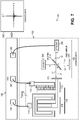
- FIGURE 7 is a diagram illustrating an exemplary architecture of the MEMS interferometer system 105, in accordance with embodiments of the present invention.
- the MEMS interferometer system 105 includes the MEMS interferometer 150 and ASIC 160.
- the MEMS interferometer 150 may be, for example, a Fourier Transform Infrared (FTIR) spectrometer that is realized over an SOI wafer to allow for a MEMS-actuated moving mirror.
- FTIR Fourier Transform Infrared
- the MEMS interferometer 150 includes the MEMS actuator 110 and interferometer 140.
- the interferometer 140 includes a light source 300, beam splitter 310, fixed mirror 320, photodetector 330 and moveable mirror 120.
- the light source 300 produces an incident beam I that travels through the interferometer 140 until it reaches the half plane beam splitter 310.
- the beam splitter 310 is formed at an interface between a first medium (i.e., silicon (Si)) and a second medium (i.e., air).
- the silicon/air interface beam splitter 310 is positioned at an angle (for example, 45 degrees) from the incident beam I.
- the desired angle may be produced, for example, by photolithographically defining a surface of the silicon medium.
- the incident beam I Upon impinging the half plane beam splitter 310, the incident beam I is split into two interfering beams L1 and L2.
- L1 originates from the partial reflection of the incident beam I from the silicon/air half plane beam splitter 310, and thus has a reflection angle equal to the beam incidence angle.
- L2 originates from the partial transmission of the incident beam I through silicon/air half plane beam splitter 310 and propagates at least partially in silicon at a refraction angle (determined by Snell's law). As a result, L1 propagates towards the moveable mirror 120, while L2 propagates towards fixed mirror 320.
- Beam L1 is reflected by moveable mirror 120, thus producing reflected beam L3, while beam L2 is reflected by fixed mirror 320, thus producing reflected beam L4.
- both beams L3 and L4 take the same optical path of L1 and L2 respectively (in the opposite direction) after reflection from mirrors 120 and 320 respectively, back towards the half plane beam splitter 310.
- the spectrometer/interferometer is used as a Fourier Transform (FT) spectrometer
- one interferometer arm is formed by beams L1/L3 and includes the beam splitter 310 and moveable mirror 120
- another interferometer arm is formed by beams L2/L4 and includes fixed mirror 320.
- An interference pattern L5 is produced from reflected beams L3 and L4 interfering at the beam splitter 310.
- the interference pattern L5 is detected by detector 330.
- the output of the detector 330 is input to the ASIC 160 via terminal 166.
- the detector 330 includes a photodetector that is assembled through micromachining in the substrate (e.g., by etching the top surface of the substrate to realize an opening within which the photodetector may be placed) or that is realized monolithically within the substrate either through doping (e.g., to realize a P-I-N diode) or partial metallization (e.g., to realize metal-semiconductor-metal MSM photodetector).
- moveable mirror 120 is movable using a SOI electrostatic MEMS actuator 110.
- the electrostatic MEMS actuator 110 is shown formed of a comb drive 115 and spring 118.
- a voltage can be applied to the comb drive 114 via terminal 114, thereby inducing a capacitance across terminals 112 and 114 and causing a displacement of the moveable mirror 120 to the desired position for reflection of the beam L1.
- OPD optical path length difference
- the capacitance across terminals 112 and 114 can be measured by the ASIC 160 via ports 162 and 164 to determine the position of the moveable mirror 120. Based on the determined moveable mirror position and the output of the detector 330, an interferogram 340 can be produced (e.g., by the DSP 170 shown in FIGURE 3 ) to identify the light wavelength and the spectral print of any material in the light path.
- the moveable mirror 120 in FIGURE 7 is shown positioned at the zero path difference between the two optical paths (L1/L3 and L2/L4).
- the moveable mirror 120 can be positioned at a distance ⁇ behind the zero path position, and the moveable mirror 120 can be moved through the zero path position such that measurements are taken on both the positive and negative sides of the zero path position.
- the source 300 is a wide band source (i.e., white light source) and the negative and positive sides may be equal or not equal.
- the complex Fourier transform of the interferogram 340 can be taken to compensate for any phase errors in the mirror position.
- mirrors 120 and 320 are metallic mirrors, where selective metallization (e.g. using a shadow mask during metallization step) is used to protect the beam splitter.
- non-metallic vertical Bragg mirrors are used to obtain a small foot print spectrometer.
- the Bragg mirrors can be realized using Deep Reactive Ion Itching (DRIE), thus producing successive vertical silicon/air interfaces.
- DRIE Deep Reactive Ion Itching
- the Bragg mirrors can be designed either to have a wide spectrum reflection response to act as simple reflectors or with a wavelength selective response, depending on the application.
- a silicon/air interface is described herein for the beam splitter 310
- other mediums providing a half wave plane beam splitter can be used to realize the invention.
- micromachined or assembled glass half-planes or other materials such as Pyrex
- other materials such as liquids or different gases, can be used instead of air to provide a degree of freedom to modify the reflection coefficient of the half plane beam splitting interface.
- FIGURE 8 is a diagram illustrating an exemplary MEMS die package 400, in accordance with the present invention.
- the MEMS interferometer 150 can be integrated with the ASIC 160 chip together on the same MEMS die package 400, thereby reducing the size, cost and complexity of the MEMS system.
- FIGURE 9 illustrates an exemplary method 500 for determining the position of a moveable mirror within a MEMS apparatus, in accordance with embodiments of the present invention.
- the method begins at 510, where an electrostatic MEMS actuator having a variable capacitance is provided coupled to the moveable mirror.
- the moveable mirror is displaced using the MEMS actuator.
- a current capacitance of the MEMS actuator is sensed, and at 540, the position of the moveable mirror is determined based on the current capacitance of the MEMS actuator.
- the capacitive sensing circuit may suffer from performance drifts due to stress, temperature, humidity, normal drift of electronic components, as well as other reasons. Such drift in the capacitive sensing circuit affects the accuracy of the position of the moveable mirror, which directly affects the spectrometer/interferometer operation. Therefore, as shown in FIGURE 10 , a calibration module 600 can be included in the MEMS interferometer 105 to calibrate the capacitive sensing circuit (CSC) 130 used for the determination of optical path difference modulation.
- the calibration module 600 is an algorithm executable by the DSP 170 and may be stored, for example, in memory 620.
- the calibration module 600 is included within the ASIC of the CSC 130, or within an additional ASIC.
- the movable mirror 120 introduces an optical path difference in one path of the interferometer 140 leading to an output interferogram from which spectrum can be extracted by Fourier transform as indicated in Equations 1 and 2 below.
- I x ⁇ ⁇ ⁇ ⁇ B v cos 2 ⁇ vx dv
- B v ⁇ ⁇ ⁇ ⁇ I x cos 2 ⁇ vx dx
- OPD optical path difference
- the accuracy of the OPD is initially calibrated using the CSC 130, as discussed above, to capacitively sense motion of the MEMS actuator 150 as the moving mirror 120 is moved through the full range of motion.
- the resulting measured capacitances are mapped to the corresponding OPD (position data 650), and then can be stored within a table 630 in a memory 620.
- a light beam 102 of a certain known wavelength ⁇ ⁇ can be injected into the MEMS interferometer 105 to calibrate the CSC 130 on the production line once for each spectrometer sample.
- the capacitive sensing curve 720 of FIGURE 11B can be used to populate the look-up table 620 of C (capacitance data 640) to x (position data 650) relation, which can then be used to determine the position of the moveable mirror 120 during subsequent operations of the MEMS interferometer 105.
- the capacitance across the MEMS actuator 150 can be measured by the CSC 130, and the measured capacitance can be provided to the DSP 170 to determine the position of the moveable mirror 120 by accessing the table 630 in memory 620.
- the calibration module 600 can further determine a correction amount 610 and provide this correction amount 610 to the DSP 170.
- the DSP 170 can use the correction amount 610 and the previously determined mirror position (based on the measured capacitance provided by the CSC 130 and the table 630 look-up) to determine a corrected mirror position. Based on the corrected moveable mirror position and the output of the interferometer 140, the DSP 170 can then produce an interferogram to identify the light wavelength and the spectral print of any material in the light path.
- the DSP 170 and/or ASIC containing the CSC 130 can generate an actuation signal to control movement of the MEMS actuator 150 to move the mirror 120 to a desired position using the correction amount 610.
- the calibration module 600 determines the correction amount 610 by determining the actual capacitance of the MEMS actuator 150 at two or more known positions of the moveable mirror 120. For example, the calibration module 600 can compare the actual measured capacitances of the MEMS actuator 150 to corresponding respective capacitances within the table 630 at the two or more known positions to calculate respective errors between the measured actual capacitances and the corresponding capacitances within the table 630. The calibration module 600 can then extrapolate a corrected capacitance sensing curve using the initial capacitance sensing curve and the calculated errors and determine the correction amount 610 to be applied to the mirror position based on the difference between the corrected capacitance sensing curve and the initial capacitance sensing curve.
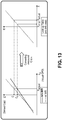
- drifts in the initial capacitance values may occur in the form of offset error (B d ) and/or gain error (A d ).
- the initial values stored in the table provide a capacitance value of B o at zero OPD with a gain of A o .
- drift in the CSC has occurred, such that the zero OPD corresponds to a capacitance value of B d and the gain is now A d .
- FIGURES 14-18 illustrate exemplary correction techniques to account for the capacitive sensing drift, thus enabling self-sustained calibration for optical path modulation of the MEMS interferometer.
- a wideband light source 800 is used to self-calibrate the MEMS interferometer.
- the error in the capacitance measurements versus the position is linear. Therefore, only two capacitance measurements at known mirror positions are needed to correct for drift errors in the C to x relation.
- the wide band light source 800 has a spectrum S(v) that is injected into the interferometer 140.
- the mirror position at the center burst 830 of the white light interferogram is irrespective of the source spectrum shape, which makes relying on that position more immune to source fluctuations and drift. Therefore, as shown in FIGURE 14 , the CSC 130 can continuously measure the capacitance of the MEMS actuator 150 while the white light interferogram is being obtained and provide the measured capacitance values to the calibration module 600. From the resulting interferogram provided by the interferometer 140, the calibration module 600 can determine the measured capacitance when the moving mirror 120 was at a burst position 820 corresponding to the center burst 830 and map that burst position 820 to zero OPD, which can be considered a first reference position for self-calibration.
- the CSC 130 can measure the capacitance of the MEMS actuator 150 when the MEMS actuator is idle (i.e., no actuation is being applied to the moving mirror 120) and provide the idle measured capacitance to the calibration module 600.
- the MEMS actuator 150 is idle, the moving mirror 120 is at a known rest position 810, which can be considered a second reference position for self-calibration.
- the calibration module 600 can determine the correction amount 610 to be applied by the DSP 170 to the capacitance sensing curve (values stored in table 630) during subsequent MEMS interferometer operations. Therefore, any capacitive sensing linear drifts in subsequent interferograms can be compensated for using the correction amount 610.
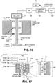
- FIGURE 16 illustrates another linear correction technique using actuator stoppers 930a-930c to self-calibrate the MEMS interferometer.
- the MEMS actuator 150 is coupled to the moving mirror 120 via an actuator arm 900.
- a fixed structure 920 surrounds the actuator arm 900, such that the actuator arm 900 lies between opposing sides of the fixed structure 920.
- the fixed structure 920 has a first stopper 930a at a first end thereof and a second stopper 930c at a second end thereof.
- the actuator arm 900 has a third stopper 930b attached thereto that is positioned between the first stopper 930a and the second stopper 930c of the fixed structure 920.
- the MEMS actuator 150 is configured to move the mirror 120 over a range extending between the first stopper 930a and the second stopper 930c of the fixed structure 920.
- the respective positions (displacements) of the moveable mirror 120 when the third stopper 930b on the actuator arm 920 is abutting the first stopper 930a and the second stopper 930c are known. Therefore, the CSC 130 can measure the capacitance of the MEMS actuator 150 when the third stopper 930b of the actuator arm 900 is abutting the first stopper 930a of the fixed structure 920, which can correspond to a first reference position of the moveable mirror 120 for self-calibration.
- the CSC 130 can measure the capacitance of the MEMS actuator 150 when the third stopper 930b of the actuator arm 900 is abutting the second stopper 930c of the fixed structure 920, which can correspond to a second reference position of the moveable mirror 120 for self-calibration. From the measured capacitances at both reference positions and the initial stored capacitances within the table 630, the calibration module 600 can determine the correction amount 610 to be applied by the DSP 170 to the capacitance sensing curve (values stored in table 630) during subsequent MEMS interferometer operations.
- combining the linear techniques illustrated in FIGURES 14 and 16 can provide for non-linear correction in MEMS interferometers where non-linear errors are present.
- Each of the techniques in FIGURES 14 and 16 uses two measurement points to determine the error.
- combining the two techniques provides four measurement points that can be used to correct for fourth degree errors.
- a fixed capacitive structure 1000 is provided on either side of the actuator arm 900, such that the actuator arm 900 is positioned between opposing sides of the fixed structure 1000.
- Each side of the fixed structure includes a plurality of capacitive sensing points 1010 with known spacing therebetween.
- the actuator arm 900 includes a plurality of capacitive fingers 1020 with known spacing therebetween.
- the actuator arm 900 is coupled to a first port (Port A) of the CSC, while the fixed structure 1000 is coupled to a second port (Port B) of the CSC to enable the CSC to measure a capacitance variation indicative of a change in capacitance between the capacitive sensing points 1010 and the capacitive fingers 1020 as the MEMS actuator 150 moves the moveable mirror 120.
- the capacitance variation can then be used by the calibration module to determine the correction amount.
- the CSC can continuously measure a respective capacitance between the capacitive sensing points 1010 and the capacitive fingers 1020 as the moveable mirror 120 moves to determine zero crossings and peaks of the capacitance variation.
- the zero crossings correspond to maximum offset between the capacitive sensing points 1010 and the capacitive fingers 1020 and the peaks correspond to minimum offset between the capacitive sensing points 1010 and the capacitive fingers 1020.
- respective actual capacitances across the MEMS actuator 150 at each of the zero crossings and the peaks can be measured at Ports C and D of the CSC.
- the calibration module can then determine reference positions of the moveable mirror 120 at each of the zero crossings and the peaks and determine the correction amount based on the actual capacitances of the MEMS actuator and the reference positions.
- the capacitive sensing calibration technique of FIGURE 17 enables N reference points to be obtained, where the spacing between capacitance zero crossings or capacitance peaks corresponds to a reference fixed period x period , as can be seen in FIGURE 18 .
- the capacitance change between the moving mirror arm 900 and the fixed structure 1000 By sensing the capacitance change between the moving mirror arm 900 and the fixed structure 1000, mirror displacement and consequently OPD can be calibrated using the capacitance zero crossings and the capacitance peaks shown in FIGURE 18 .
- FIGURE 19 illustrates an exemplary method 1900 for self-calibration for mirror positioning within an optical MEMS interferometer, in accordance with embodiments of the present invention.
- the method begins at 1910, where an initial calibration of the mirror position is performed to populate a table of initial values of the MEMS actuator capacitance and corresponding mirror position.
- the MEMS actuator capacitance is again measured at two or more known positions of the mirror.
- a correction amount to be applied to the initial values stored in the table is determined based on the measured capacitances at the known positions.
Landscapes
- Physics & Mathematics (AREA)
- Spectroscopy & Molecular Physics (AREA)
- General Physics & Mathematics (AREA)
- Optics & Photonics (AREA)
- Spectrometry And Color Measurement (AREA)
- Mechanical Light Control Or Optical Switches (AREA)
Claims (11)
- Ein mikro-elektromechanisches System (MEMS) (100), umfassend:- einen beweglichen Spiegel (120);- ein MEMS-Stellglied (110, 150), verbunden mit dem beweglichen Spiegel (120), um diesen zu verstellen, das MEMS-Stellglied (110, 150) hat dabei eine variable Kapazität;- einen Speicher zur Aufrechterhaltung der Tabellenabbildungs-Kapazität (630) des MEMS-Stellgliedes (110, 150) zur Positionierung des beweglichen Spiegels (120);- einen kapazitiven Messkreis (130), verbunden mit dem MEMS-Stellglied (110, 150), zur Messung der aktuellen Kapazität des MEMS-Stellgliedes (120);- einen digitalen Signalprozessor (170) um auf die Tabelle (630) zugreifen zu können, um die aktuelle Position des beweglichen Spiegels (120) auf Grundlage der aktuellen Kapazität des MEMS-Stellgliedes (110, 150) zu bestimmen; und- ein Kalibriermodul (600) zur Korrektur einer Drift der aktuellen Kapazität des MEMS-Stellgliedes (110, 150) und folglich des Verhältnisses zwischen der aktuellen Kapazität und der aktuellen Position des beweglichen Spiegels (120) durch Bestimmung der jeweiligen aktuellen Kapazität des MEMS-Stellgliedes (110, 150) an zwei oder mehr bekannten Positionen des beweglichen Spiegels (120) zur Bestimmung des Korrekturumfangs, der auf die aktuelle Position des beweglichen Spiegels auszuüben ist, wobei die bekannte Position des beweglichen Spiegel entweder die Burst- Position, die Ruheposition oder die Endposition umfasst, definiert durch Stopper und Spitzen oder Nulldurchgänge, gemessen mit kapazitiven Fingern;- eine Breitband-Lichtquelle zur Erzeugung eines Breitband-Lichtstrahls;- ein Interferometer (140), das enthält:• einen Strahlteiler (130), der optisch so verbunden ist, dass er den Breitband-Lichtstrahl empfängt und den Breitband-Lichtstrahl in einen ersten Interferenzstrahl und einen zweiten Interferenzstrahl teilt;• einen festen Spiegel (320), der optisch so verbunden ist, dass er den Breitband-Lichtstrahl empfängt und den ersten Interferenz-Lichtstrahl zurück zum Strahlteiler reflektiert, so dass er einen ersten reflektierten Interferenz-Lichtstrahl erzeugt;• den beweglichen Spiegel (120), der optisch so verbunden ist, dass er den zweiten Interferenz-Lichtstrahl empfängt und den zweiten Interferenz-Lichtstrahl zurück zum Strahlteiler reflektiert, so dass er einen zweiten reflektierten Interferenz-Lichtstrahl erzeugt; die Verstellung des beweglichen Spiegels erzeugt eine optische Pfadlängendifferenz zwischen dem ersten und dem zweiten Interferenz-Lichtstrahl, gleich dem Doppelten der Verstellung; und• einen Detektor (330), optisch verbunden zur Erkennung eines Interferenzmusters, das als Ergebnis der Interferenz zwischen dem ersten reflektierten Interferenz-Lichtstrahl und dem zweiten reflektierten Interferenz-Lichtstrahl erzeugt wird; wobei der kapazitive Messkreis (130) eine erste gemessene Kapazität an einer ersten bekannten Position des beweglichen Spiegels bestimmt, die einem Mitten-Burst eines Interferenz- Musters entspricht, erzeugt als Ergebnis des Breitband-Lichtstrahls und der Bewegung des beweglichen Spiegels;
wobei der kapazitive Messkreis (130) eine zweite gemessene Kapazität an einer zweiten bekannten Position des beweglichen Spiegels bestimmt, die einer Null-Betätigung des beweglichen Spiegels durch das MEMS-Stellglied entspricht; wobei das Kalibriermodul (600) die erste gemessene Kapazität an der ersten bekannten Position und die zweite gemessene Kapazität an der zweiten bekannten Position zur Bestimmung des Korrekturumfanges nutzt;
wobei sich die erste bekannte Position von der zweiten bekannten Position unterscheidet;
wobei der digitale Signalprozessor (170) weiterhin eine korrigierte aktuelle Position des beweglichen Spiegels (120), unter Verwendung des Korrekturumfangs, erzeugt. - Mikro-elektromechanisches System (MEMS) (100), umfassend:- einen beweglichen Spiegel (120);- ein MEMS-Stellglied (110, 150), verbunden mit dem beweglichen Spiegel (120) um diesen zu verstellen, das MEMS-Stellglied (110, 150) hat dabei eine variable Kapazität;- einen Speicher zur Aufrechterhaltung der Tabellenabbildungs-Kapazität (630) des MEMS-Stellgliedes (110, 150) zur Positionierung des beweglichen Spiegels (120);- einen kapazitiven Messkreis (130), verbunden mit dem MEMS-Stellglied (110, 150), zur Messung der aktuellen Kapazität des MEMS-Stellgliedes (120);- einen digitalen Signalprozessor (170), um auf die Tabelle (630) zugreifen zu können, um eine aktuelle Position des beweglichen Spiegels (120) auf Grundlage der aktuellen Kapazität des MEMS-Stellgliedes (110, 150) zu bestimmen; und- ein Kalibriermodul (600) zur Korrektur einer Drift der aktuellen Kapazität des MEMS-Stellgliedes (110, 150) und folglich des Verhältnisses zwischen der aktuellen Kapazität und der aktuellen Position des beweglichen Spiegels (120) durch Bestimmung der jeweiligen aktuellen Kapazität des MEMS-Stellgliedes (110, 150) an zwei oder mehr bekannten Positionen des beweglichen Spiegels (120) zur Bestimmung des Korrekturumfangs, der auf die aktuelle Position des beweglichen Spiegels auszuüben ist,- eine feste Struktur mit einem ersten Stopper (930A) an einem ersten Ende und einem zweiten Stopper (930C) an einem zweiten Ende;- einen Stellgliedarm (900), angeschlossen zwischen dem MEMS-Stellglied (150) und dem beweglichen Spiegel (120), der Stellgliedarm (900) verfügt über einen dritten Stopper (930B), wobei der dritte Stopper (930B) zwischen dem ersten Stopper (930A) und dem zweiten Stopper (930C) angeordnet ist;
wobei der kapazitive Messkreis (130) eine erste gemessene Kapazität an einer ersten bekannten Referenzposition des beweglichen Spiegels bestimmt, wenn der dritte Stopper (930B) gegen den ersten Stopper (930A) stößt;
wobei der kapazitive Messkreis (130) eine zweite gemessene Kapazität an einer zweiten bekannten Referenzposition des beweglichen Spiegels bestimmt, wenn der dritte Stopper (930B) gegen den zweiten Stopper (930C) stößt;
wobei das Kalibriermodul (600) die erste gemessene Kapazität an der ersten bekannten Position und die zweite gemessene Kapazität an der zweiten bekannten Position zur Bestimmung des Korrekturumfanges nutzt;
wobei der digitale Signalprozessor (170) weiterhin eine korrigierte aktuelle Position des beweglichen Spiegels (120), unter Verwendung des Korrekturumfangs, erzeugt. - Mikro-elektromechanisches System (MEMS) (100), umfassend:- einen beweglichen Spiegel (120);- ein MEMS-Stellglied (110, 150) verbunden mit dem beweglichen Spiegel (120) um diesen zu verstellen, das MEMS-Stellglied (110, 150) hat dabei eine variable Kapazität;- einen Speicher zur Aufrechterhaltung der Tabellenabbildungs-Kapazität (630) des MEMS-Stellgliedes (110, 150) zur Positionierung des beweglichen Spiegels (120);- einen kapazitiven Messkreis (130), verbunden mit dem MEMS-Stellglied (110, 150), zur Messung der aktuellen Kapazität des MEMS-Stellgliedes (120);- einen digitalen Signalprozessor (170), um auf die Tabelle (630) zugreifen zu können, um eine aktuelle Position des beweglichen Spiegels (120) auf Grundlage der aktuellen Kapazität des MEMS-Stellgliedes (110, 150) zu bestimmen; und- ein Kalibriermodul (600) zur Korrektur einer Drift der aktuellen Kapazität des MEMS-Stellgliedes (110, 150) und folglich des Verhältnisses zwischen der aktuellen Kapazität und der aktuellen Position des beweglichen Spiegels (120) durch Bestimmung der jeweiligen aktuellen Kapazität des MEMS-Stellgliedes (110, 150) an zwei oder mehr bekannten Positionen des beweglichen Spiegels (120) zur Bestimmung des Korrekturumfangs, der auf die aktuelle Position des beweglichen Spiegels auszuüben ist,- eine feste Struktur (1000) mit einer ersten Seite und einer zweiten Seite gegenüber der ersten Seite, wobei sowohl die erste wie die zweite Seite mehrere kapazitive Messpunkte (1010) enthalten, deren Abstände voneinander bekannt sind;- ein Stellgliedarm (900), gekoppelt zwischen das MEMS-Stellglied (150) und den beweglichen Spiegel (120) und zwischen der ersten Seite und der zweiten Seite der kapazitiven Struktur beweglich, der Stellgliedarm verfügt dabei über mehrere kapazitive Finger (1020) mit bekannten Abständen voneinander;
wobei der kapazitive Messkreis (130) mit der festen Struktur und dem (1000) Stellgliedarm (900) verbunden ist, zur Messung eines Kapazitätsschwankungssignals, das auf eine Änderung der Kapazität zwischen den kapazitiven Messpunkten (1010) und den kapazitiven Fingern (1020) hinweist, wenn sich der bewegliche Spiegel bewegt,
wobei der kapazitive Messkreis (130) ständig die jeweilige Kapazität zwischen den kapazitiven Messpunkten (1010) und den kapazitiven Fingern (1020) misst, während sich der bewegliche Spiegel (120) bewegt, um Nulldurchgänge und Spitzen der Kapazitätsschwankung weiter zu bestimmen, die Nulldurchgänge entsprechen dem maximalen Versatz zwischen den kapazitiven Messpunkten (1010) und den kapazitiven Fingern (1020) und die Spitzen entsprechen dem minimalen Versatz zwischen den kapazitiven Messpunkten (1010) und den kapazitiven Fingern (1020); wobei der kapazitive Messkreis (130) weiterhin die jeweilige aktuelle Kapazität des MEMS-Stellgliedes bei jedem der Nulldurchgänge und der Spitzen bestimmt; wobei das Kalibriermodul (600) bekannte Referenzpositionen des beweglichen Spiegels bei jedem der Nulldurchgänge und der Spitzen bestimmt;
wobei das Kalibriermodul den Korrekturumfang auf Grundlage der aktuellen Kapazitäten des MEMS-Stellgliedes und der bekannten Referenzpositionen bestimmt;
wobei der digitale Signalprozessor (170) weiterhin eine korrigierte aktuelle Position des beweglichen Spiegels (120), unter Verwendung des Korrekturumfangs, erzeugt. - MEMS-Gerät nach Anspruch 1,
wobei der kapazitiver Messkreis (130) eine Kapazitätsschwankung misst, wenn sich der bewegliche Spiegel (120) durch mindestens zwei Nulldurchgänge des Interferenzmusters bewegt; und
wobei der digitale Signalprozessor (170) die Tabelle (630) auf Basis der Kapazitätsschwankungen und des Interferenzmusters füllt. - MEMS-Gerät nach Anspruch 1 oder 4, wobei;- die Tabelle (630) eine Kapazitätsmesskurve darstellt;- das Kalibriermodul (600) die aktuelle Kapazität des MEMS-Stellgliedes (110) mit entsprechenden jeweiligen Kapazitäten innerhalb der Tabelle (630) an den zwei oder mehr bekannten Positionen vergleicht, um jeweilige Fehler zwischen der gemessenen aktuellen Kapazität und der entsprechenden Kapazität innerhalb der Tabelle (630) zu berechnen;- das Kalibriermodul (600) extrapoliert eine korrigierte Kapazitätsmesskurve unter Verwendung der Kapazitätsmesskurve und der berechneten Fehler; und- das Kalibriermodul (600) verwendet die korrigierte Kapazitätsmesskurve zur Bestimmung des Korrekturumfangs, der auf die aktuelle Position anzuwenden ist.
- MEMS-Gerät nach Anspruch 2, weiterhin umfassend:- eine Breitband-Lichtquelle zur Erzeugung eines Breitband-Lichtstrahls;- ein Interferometer, der enthält:• einen Strahlteiler (310), der optisch so verbunden ist, dass er den Breitband-Lichtstrahl empfängt und den Breitband-Lichtstrahl in einen ersten Interferenzstrahl und einen zweiten Interferenzstrahl teilt;• einen festen Spiegel (320), der optisch so verbunden ist, dass er den Breitband-Lichtstrahl empfängt und den ersten Interferenz-Lichtstrahl zurück zum Strahlteiler (310) reflektiert, so dass er einen ersten reflektierten Interferenz-Lichtstrahl erzeugt;• den beweglichen Spiegel (120), der optisch so verbunden ist, dass er den zweiten Interferenz-Lichtstrahl empfängt und den zweiten Interferenz-Lichtstrahl zurück zum Strahlteiler (310) reflektiert, so dass er einen zweiten reflektierten Interferenz-Lichtstrahl erzeugt; die Verstellung des beweglichen Spiegels (120) erzeugt eine optische Pfadlängendifferenz zwischen dem ersten und zweiten Interferenz-Lichtstrahlen, gleich dem Doppelten der Verstellung; und• einen Detektor (330), optisch verbunden zur Erkennung eines Interferenzmusters, das als Ergebnis der Interferenz zwischen dem ersten reflektierten Interferenz-Lichtstrahl und dem zweiten reflektierten Interferenz-Lichtstrahl erzeugt wird; wobei der kapazitive Messkreis (130) eine dritte gemessene Kapazität an einer dritten bekannten Referenzposition des beweglichen Spiegels bestimmt, die dem Mitten-Burst eines Interferenzmusters entspricht, erzeugt als Ergebnis des Breitband-Lichtstrahls und der Bewegung des beweglichen Spiegels;
wobei der kapazitiver Messkreis (130) eine vierte gemessene Kapazität an einer vierten bekannten Referenzposition des beweglichen Spiegels bestimmt, die der Null-Betätigung des beweglichen Spiegels durch das MEMS-Stellglied entspricht; und
wobei das Kalibriermodul (600) die erste gemessene Kapazität an der ersten bekannten Referenzposition, die zweite gemessene Kapazität an der zweiten bekannten Referenzposition, die dritte gemessene Kapazität an der dritten bekannten Referenzposition und die vierte gemessene Kapazität an der vierten bekannten Referenzposition zur Bestimmung des Korrekturumfangs nutzt;
wobei die dritte bekannte Referenzposition sich von der vierten bekannten Referenzposition unterscheidet. - MEMS-Gerät nach irgendeinem der Ansprüche 1 bis 6, wobei es sich bei dem MEMS-Stellglied (110) um ein elektrostatisches Stellglied mit zwei Platten handelt, der kapazitive Messkreis misst dabei die aktuelle Kapazität zwischen den beiden Platten.
- MEMS-Gerät nach Anspruch 1, wobei es sich bei dem MEMS-Stellglied (150) um ein elektrostatisches Kammantriebs- Stellglied handelt.
- MEMS-Gerät nach irgendeinem der Ansprüche 1 bis 6, wobei der kapazitive Messkreis (130) einen Kapazitäts-/Spannungswandler enthält, zum Empfang der aktuellen Kapazität und zur Erzeugung einer Ausgabespannung proportional zur Kapazität.
- Mikro-elektromechanisches Interferometer-System (MEMS), umfassend ein MEMS-Gerät, nach irgendeinem der Ansprüche 1 bis 9.
- Das MEMS-Interferometer-System nach Anspruch 10, wobei es sich bei dem Interferometer um ein Fourier Transform Infrared (FTIR)-Spektrometer handelt.
Applications Claiming Priority (2)
| Application Number | Priority Date | Filing Date | Title |
|---|---|---|---|
| US201361757581P | 2013-01-28 | 2013-01-28 | |
| PCT/US2014/013399 WO2014117158A1 (en) | 2013-01-28 | 2014-01-28 | Self calibration for mirror positioning in optical mems interferometers |
Publications (2)
| Publication Number | Publication Date |
|---|---|
| EP2948812A1 EP2948812A1 (de) | 2015-12-02 |
| EP2948812B1 true EP2948812B1 (de) | 2020-04-01 |
Family
ID=54345367
Family Applications (1)
| Application Number | Title | Priority Date | Filing Date |
|---|---|---|---|
| EP14704976.1A Active EP2948812B1 (de) | 2013-01-28 | 2014-01-28 | Selbsteichung für eine spiegelpositionierung bei optischen mems-interferometern |
Country Status (1)
| Country | Link |
|---|---|
| EP (1) | EP2948812B1 (de) |
Families Citing this family (2)
| Publication number | Priority date | Publication date | Assignee | Title |
|---|---|---|---|---|
| CN114963998B (zh) * | 2022-05-09 | 2025-05-30 | 国科大杭州高等研究院 | 一种用于精密激光干涉测量标定的亚纳米级高精度微位移装置及应用 |
| CN119743881B (zh) * | 2025-03-05 | 2025-05-02 | 深圳市金鼎胜光电股份有限公司 | 光学检测光源标定方法、装置、设备及存储介质 |
-
2014
- 2014-01-28 EP EP14704976.1A patent/EP2948812B1/de active Active
Non-Patent Citations (1)
| Title |
|---|
| None * |
Also Published As
| Publication number | Publication date |
|---|---|
| EP2948812A1 (de) | 2015-12-02 |
Similar Documents
| Publication | Publication Date | Title |
|---|---|---|
| US8873125B2 (en) | Technique to determine mirror position in optical interferometers | |
| US9658053B2 (en) | Self calibration for mirror positioning in optical MEMS interferometers | |
| US9658107B2 (en) | Self calibration for mirror positioning in optical MEMS interferometers | |
| WO2014117158A1 (en) | Self calibration for mirror positioning in optical mems interferometers | |
| EP1906159B1 (de) | System, Verfahren und Vorrichtung für ein mikrogefertigtes Interferometer mit optischem Strahlteiler | |
| EP2475970B1 (de) | Kompensierte mems-ftir-spektrometerarchitektur | |
| JP5725165B2 (ja) | フーリエ変換型分光計およびフーリエ変換型分光方法 | |
| EP3390991B1 (de) | Selbstkalibrierung für eine spiegelpositionierung bei optischen mems-interferometern | |
| Sandner et al. | Miniaturized FTIR-spectrometer based on an optical MEMS translatory actuator | |
| CN107144537A (zh) | 一种可见光傅里叶变换吸收光谱测量方法及系统 | |
| EP2948812B1 (de) | Selbsteichung für eine spiegelpositionierung bei optischen mems-interferometern | |
| US8508745B2 (en) | System, method and apparatus for a micromachined interferometer using optical splitting | |
| WO2012124294A1 (ja) | フーリエ変換型分光計およびフーリエ変換型分光方法 | |
| Mishra | Design Analysis and Performance Evaluation of Fiberoptic Pressure Sensors Based on Fabry-Perot Interferometer | |
| CN114034300A (zh) | 光学加速度计和惯性导航系统 | |
| CN115943293A (zh) | 傅里叶变换光谱仪和傅里叶变换光谱方法 |
Legal Events
| Date | Code | Title | Description |
|---|---|---|---|
| PUAI | Public reference made under article 153(3) epc to a published international application that has entered the european phase |
Free format text: ORIGINAL CODE: 0009012 |
|
| 17P | Request for examination filed |
Effective date: 20150810 |
|
| AK | Designated contracting states |
Kind code of ref document: A1 Designated state(s): AL AT BE BG CH CY CZ DE DK EE ES FI FR GB GR HR HU IE IS IT LI LT LU LV MC MK MT NL NO PL PT RO RS SE SI SK SM TR |
|
| AX | Request for extension of the european patent |
Extension state: BA ME |
|
| DAX | Request for extension of the european patent (deleted) | ||
| STAA | Information on the status of an ep patent application or granted ep patent |
Free format text: STATUS: EXAMINATION IS IN PROGRESS |
|
| 17Q | First examination report despatched |
Effective date: 20180221 |
|
| GRAP | Despatch of communication of intention to grant a patent |
Free format text: ORIGINAL CODE: EPIDOSNIGR1 |
|
| STAA | Information on the status of an ep patent application or granted ep patent |
Free format text: STATUS: GRANT OF PATENT IS INTENDED |
|
| INTG | Intention to grant announced |
Effective date: 20191209 |
|
| GRAS | Grant fee paid |
Free format text: ORIGINAL CODE: EPIDOSNIGR3 |
|
| GRAA | (expected) grant |
Free format text: ORIGINAL CODE: 0009210 |
|
| STAA | Information on the status of an ep patent application or granted ep patent |
Free format text: STATUS: THE PATENT HAS BEEN GRANTED |
|
| AK | Designated contracting states |
Kind code of ref document: B1 Designated state(s): AL AT BE BG CH CY CZ DE DK EE ES FI FR GB GR HR HU IE IS IT LI LT LU LV MC MK MT NL NO PL PT RO RS SE SI SK SM TR |
|
| REG | Reference to a national code |
Ref country code: GB Ref legal event code: FG4D |
|
| REG | Reference to a national code |
Ref country code: AT Ref legal event code: REF Ref document number: 1252125 Country of ref document: AT Kind code of ref document: T Effective date: 20200415 Ref country code: CH Ref legal event code: EP |
|
| REG | Reference to a national code |
Ref country code: DE Ref legal event code: R096 Ref document number: 602014063104 Country of ref document: DE |
|
| REG | Reference to a national code |
Ref country code: NL Ref legal event code: FP |
|
| REG | Reference to a national code |
Ref country code: IE Ref legal event code: FG4D |
|
| REG | Reference to a national code |
Ref country code: FI Ref legal event code: FGE |
|
| REG | Reference to a national code |
Ref country code: SE Ref legal event code: TRGR |
|
| PG25 | Lapsed in a contracting state [announced via postgrant information from national office to epo] |
Ref country code: BG Free format text: LAPSE BECAUSE OF FAILURE TO SUBMIT A TRANSLATION OF THE DESCRIPTION OR TO PAY THE FEE WITHIN THE PRESCRIBED TIME-LIMIT Effective date: 20200701 |
|
| REG | Reference to a national code |
Ref country code: LT Ref legal event code: MG4D |
|
| PG25 | Lapsed in a contracting state [announced via postgrant information from national office to epo] |
Ref country code: GR Free format text: LAPSE BECAUSE OF FAILURE TO SUBMIT A TRANSLATION OF THE DESCRIPTION OR TO PAY THE FEE WITHIN THE PRESCRIBED TIME-LIMIT Effective date: 20200702 Ref country code: NO Free format text: LAPSE BECAUSE OF FAILURE TO SUBMIT A TRANSLATION OF THE DESCRIPTION OR TO PAY THE FEE WITHIN THE PRESCRIBED TIME-LIMIT Effective date: 20200701 Ref country code: IS Free format text: LAPSE BECAUSE OF FAILURE TO SUBMIT A TRANSLATION OF THE DESCRIPTION OR TO PAY THE FEE WITHIN THE PRESCRIBED TIME-LIMIT Effective date: 20200801 Ref country code: CZ Free format text: LAPSE BECAUSE OF FAILURE TO SUBMIT A TRANSLATION OF THE DESCRIPTION OR TO PAY THE FEE WITHIN THE PRESCRIBED TIME-LIMIT Effective date: 20200401 Ref country code: PT Free format text: LAPSE BECAUSE OF FAILURE TO SUBMIT A TRANSLATION OF THE DESCRIPTION OR TO PAY THE FEE WITHIN THE PRESCRIBED TIME-LIMIT Effective date: 20200817 Ref country code: LT Free format text: LAPSE BECAUSE OF FAILURE TO SUBMIT A TRANSLATION OF THE DESCRIPTION OR TO PAY THE FEE WITHIN THE PRESCRIBED TIME-LIMIT Effective date: 20200401 |
|
| REG | Reference to a national code |
Ref country code: AT Ref legal event code: MK05 Ref document number: 1252125 Country of ref document: AT Kind code of ref document: T Effective date: 20200401 |
|
| PG25 | Lapsed in a contracting state [announced via postgrant information from national office to epo] |
Ref country code: HR Free format text: LAPSE BECAUSE OF FAILURE TO SUBMIT A TRANSLATION OF THE DESCRIPTION OR TO PAY THE FEE WITHIN THE PRESCRIBED TIME-LIMIT Effective date: 20200401 Ref country code: RS Free format text: LAPSE BECAUSE OF FAILURE TO SUBMIT A TRANSLATION OF THE DESCRIPTION OR TO PAY THE FEE WITHIN THE PRESCRIBED TIME-LIMIT Effective date: 20200401 Ref country code: LV Free format text: LAPSE BECAUSE OF FAILURE TO SUBMIT A TRANSLATION OF THE DESCRIPTION OR TO PAY THE FEE WITHIN THE PRESCRIBED TIME-LIMIT Effective date: 20200401 |
|
| PG25 | Lapsed in a contracting state [announced via postgrant information from national office to epo] |
Ref country code: AL Free format text: LAPSE BECAUSE OF FAILURE TO SUBMIT A TRANSLATION OF THE DESCRIPTION OR TO PAY THE FEE WITHIN THE PRESCRIBED TIME-LIMIT Effective date: 20200401 |
|
| REG | Reference to a national code |
Ref country code: DE Ref legal event code: R097 Ref document number: 602014063104 Country of ref document: DE |
|
| PG25 | Lapsed in a contracting state [announced via postgrant information from national office to epo] |
Ref country code: ES Free format text: LAPSE BECAUSE OF FAILURE TO SUBMIT A TRANSLATION OF THE DESCRIPTION OR TO PAY THE FEE WITHIN THE PRESCRIBED TIME-LIMIT Effective date: 20200401 Ref country code: DK Free format text: LAPSE BECAUSE OF FAILURE TO SUBMIT A TRANSLATION OF THE DESCRIPTION OR TO PAY THE FEE WITHIN THE PRESCRIBED TIME-LIMIT Effective date: 20200401 Ref country code: SM Free format text: LAPSE BECAUSE OF FAILURE TO SUBMIT A TRANSLATION OF THE DESCRIPTION OR TO PAY THE FEE WITHIN THE PRESCRIBED TIME-LIMIT Effective date: 20200401 Ref country code: AT Free format text: LAPSE BECAUSE OF FAILURE TO SUBMIT A TRANSLATION OF THE DESCRIPTION OR TO PAY THE FEE WITHIN THE PRESCRIBED TIME-LIMIT Effective date: 20200401 Ref country code: EE Free format text: LAPSE BECAUSE OF FAILURE TO SUBMIT A TRANSLATION OF THE DESCRIPTION OR TO PAY THE FEE WITHIN THE PRESCRIBED TIME-LIMIT Effective date: 20200401 Ref country code: IT Free format text: LAPSE BECAUSE OF FAILURE TO SUBMIT A TRANSLATION OF THE DESCRIPTION OR TO PAY THE FEE WITHIN THE PRESCRIBED TIME-LIMIT Effective date: 20200401 Ref country code: RO Free format text: LAPSE BECAUSE OF FAILURE TO SUBMIT A TRANSLATION OF THE DESCRIPTION OR TO PAY THE FEE WITHIN THE PRESCRIBED TIME-LIMIT Effective date: 20200401 |
|
| PLBE | No opposition filed within time limit |
Free format text: ORIGINAL CODE: 0009261 |
|
| STAA | Information on the status of an ep patent application or granted ep patent |
Free format text: STATUS: NO OPPOSITION FILED WITHIN TIME LIMIT |
|
| PG25 | Lapsed in a contracting state [announced via postgrant information from national office to epo] |
Ref country code: PL Free format text: LAPSE BECAUSE OF FAILURE TO SUBMIT A TRANSLATION OF THE DESCRIPTION OR TO PAY THE FEE WITHIN THE PRESCRIBED TIME-LIMIT Effective date: 20200401 Ref country code: SK Free format text: LAPSE BECAUSE OF FAILURE TO SUBMIT A TRANSLATION OF THE DESCRIPTION OR TO PAY THE FEE WITHIN THE PRESCRIBED TIME-LIMIT Effective date: 20200401 |
|
| 26N | No opposition filed |
Effective date: 20210112 |
|
| PG25 | Lapsed in a contracting state [announced via postgrant information from national office to epo] |
Ref country code: SI Free format text: LAPSE BECAUSE OF FAILURE TO SUBMIT A TRANSLATION OF THE DESCRIPTION OR TO PAY THE FEE WITHIN THE PRESCRIBED TIME-LIMIT Effective date: 20200401 |
|
| PG25 | Lapsed in a contracting state [announced via postgrant information from national office to epo] |
Ref country code: MC Free format text: LAPSE BECAUSE OF FAILURE TO SUBMIT A TRANSLATION OF THE DESCRIPTION OR TO PAY THE FEE WITHIN THE PRESCRIBED TIME-LIMIT Effective date: 20200401 |
|
| REG | Reference to a national code |
Ref country code: CH Ref legal event code: PL |
|
| PG25 | Lapsed in a contracting state [announced via postgrant information from national office to epo] |
Ref country code: LU Free format text: LAPSE BECAUSE OF NON-PAYMENT OF DUE FEES Effective date: 20210128 |
|
| REG | Reference to a national code |
Ref country code: BE Ref legal event code: MM Effective date: 20210131 |
|
| PG25 | Lapsed in a contracting state [announced via postgrant information from national office to epo] |
Ref country code: LI Free format text: LAPSE BECAUSE OF NON-PAYMENT OF DUE FEES Effective date: 20210131 Ref country code: CH Free format text: LAPSE BECAUSE OF NON-PAYMENT OF DUE FEES Effective date: 20210131 |
|
| PG25 | Lapsed in a contracting state [announced via postgrant information from national office to epo] |
Ref country code: IE Free format text: LAPSE BECAUSE OF NON-PAYMENT OF DUE FEES Effective date: 20210128 |
|
| PG25 | Lapsed in a contracting state [announced via postgrant information from national office to epo] |
Ref country code: BE Free format text: LAPSE BECAUSE OF NON-PAYMENT OF DUE FEES Effective date: 20210131 |
|
| PG25 | Lapsed in a contracting state [announced via postgrant information from national office to epo] |
Ref country code: HU Free format text: LAPSE BECAUSE OF FAILURE TO SUBMIT A TRANSLATION OF THE DESCRIPTION OR TO PAY THE FEE WITHIN THE PRESCRIBED TIME-LIMIT; INVALID AB INITIO Effective date: 20140128 |
|
| PG25 | Lapsed in a contracting state [announced via postgrant information from national office to epo] |
Ref country code: CY Free format text: LAPSE BECAUSE OF FAILURE TO SUBMIT A TRANSLATION OF THE DESCRIPTION OR TO PAY THE FEE WITHIN THE PRESCRIBED TIME-LIMIT Effective date: 20200401 |
|
| PGFP | Annual fee paid to national office [announced via postgrant information from national office to epo] |
Ref country code: NL Payment date: 20231229 Year of fee payment: 11 Ref country code: FI Payment date: 20231222 Year of fee payment: 11 |
|
| PG25 | Lapsed in a contracting state [announced via postgrant information from national office to epo] |
Ref country code: MK Free format text: LAPSE BECAUSE OF FAILURE TO SUBMIT A TRANSLATION OF THE DESCRIPTION OR TO PAY THE FEE WITHIN THE PRESCRIBED TIME-LIMIT Effective date: 20200401 |
|
| PGFP | Annual fee paid to national office [announced via postgrant information from national office to epo] |
Ref country code: GB Payment date: 20240119 Year of fee payment: 11 |
|
| PG25 | Lapsed in a contracting state [announced via postgrant information from national office to epo] |
Ref country code: MT Free format text: LAPSE BECAUSE OF FAILURE TO SUBMIT A TRANSLATION OF THE DESCRIPTION OR TO PAY THE FEE WITHIN THE PRESCRIBED TIME-LIMIT Effective date: 20200401 |
|
| REG | Reference to a national code |
Ref country code: NL Ref legal event code: MM Effective date: 20250201 |
|
| GBPC | Gb: european patent ceased through non-payment of renewal fee |
Effective date: 20250128 |
|
| PG25 | Lapsed in a contracting state [announced via postgrant information from national office to epo] |
Ref country code: FI Free format text: LAPSE BECAUSE OF NON-PAYMENT OF DUE FEES Effective date: 20250128 |
|
| PG25 | Lapsed in a contracting state [announced via postgrant information from national office to epo] |
Ref country code: NL Free format text: LAPSE BECAUSE OF NON-PAYMENT OF DUE FEES Effective date: 20250201 |
|
| PG25 | Lapsed in a contracting state [announced via postgrant information from national office to epo] |
Ref country code: GB Free format text: LAPSE BECAUSE OF NON-PAYMENT OF DUE FEES Effective date: 20250128 |
|
| PG25 | Lapsed in a contracting state [announced via postgrant information from national office to epo] |
Ref country code: TR Free format text: LAPSE BECAUSE OF FAILURE TO SUBMIT A TRANSLATION OF THE DESCRIPTION OR TO PAY THE FEE WITHIN THE PRESCRIBED TIME-LIMIT Effective date: 20200401 |
|
| REG | Reference to a national code |
Ref country code: DE Ref legal event code: R082 Ref document number: 602014063104 Country of ref document: DE Representative=s name: VUILLERMOZ, BRUNO, FR |
|
| PGFP | Annual fee paid to national office [announced via postgrant information from national office to epo] |
Ref country code: SE Payment date: 20260127 Year of fee payment: 13 |
|
| PGFP | Annual fee paid to national office [announced via postgrant information from national office to epo] |
Ref country code: DE Payment date: 20260114 Year of fee payment: 13 |
|
| PGFP | Annual fee paid to national office [announced via postgrant information from national office to epo] |
Ref country code: FR Payment date: 20260127 Year of fee payment: 13 |