EP2946474B1 - N-well switching circuit - Google Patents
N-well switching circuit Download PDFInfo
- Publication number
- EP2946474B1 EP2946474B1 EP14702369.1A EP14702369A EP2946474B1 EP 2946474 B1 EP2946474 B1 EP 2946474B1 EP 14702369 A EP14702369 A EP 14702369A EP 2946474 B1 EP2946474 B1 EP 2946474B1
- Authority
- EP
- European Patent Office
- Prior art keywords
- voltage
- well
- pmos transistor
- oxide
- switched
- Prior art date
- Legal status (The legal status is an assumption and is not a legal conclusion. Google has not performed a legal analysis and makes no representation as to the accuracy of the status listed.)
- Not-in-force
Links
Images

Classifications
-
- H—ELECTRICITY
- H03—ELECTRONIC CIRCUITRY
- H03K—PULSE TECHNIQUE
- H03K17/00—Electronic switching or gating, i.e. not by contact-making and –breaking
- H03K17/22—Modifications for ensuring a predetermined initial state when the supply voltage has been applied
- H03K17/223—Modifications for ensuring a predetermined initial state when the supply voltage has been applied in field-effect transistor switches
-
- G—PHYSICS
- G11—INFORMATION STORAGE
- G11C—STATIC STORES
- G11C17/00—Read-only memories programmable only once; Semi-permanent stores, e.g. manually-replaceable information cards
- G11C17/14—Read-only memories programmable only once; Semi-permanent stores, e.g. manually-replaceable information cards in which contents are determined by selectively establishing, breaking or modifying connecting links by permanently altering the state of coupling elements, e.g. PROM
- G11C17/18—Auxiliary circuits, e.g. for writing into memory
-
- G—PHYSICS
- G11—INFORMATION STORAGE
- G11C—STATIC STORES
- G11C7/00—Arrangements for writing information into, or reading information out from, a digital store
-
- G—PHYSICS
- G11—INFORMATION STORAGE
- G11C—STATIC STORES
- G11C7/00—Arrangements for writing information into, or reading information out from, a digital store
- G11C7/12—Bit line control circuits, e.g. drivers, boosters, pull-up circuits, pull-down circuits, precharging circuits, equalising circuits, for bit lines
-
- G—PHYSICS
- G11—INFORMATION STORAGE
- G11C—STATIC STORES
- G11C8/00—Arrangements for selecting an address in a digital store
- G11C8/08—Word line control circuits, e.g. drivers, boosters, pull-up circuits, pull-down circuits, precharging circuits, for word lines
-
- H—ELECTRICITY
- H03—ELECTRONIC CIRCUITRY
- H03K—PULSE TECHNIQUE
- H03K17/00—Electronic switching or gating, i.e. not by contact-making and –breaking
- H03K17/08—Modifications for protecting switching circuit against overcurrent or overvoltage
- H03K17/081—Modifications for protecting switching circuit against overcurrent or overvoltage without feedback from the output circuit to the control circuit
- H03K17/08104—Modifications for protecting switching circuit against overcurrent or overvoltage without feedback from the output circuit to the control circuit in field-effect transistor switches
-
- H—ELECTRICITY
- H03—ELECTRONIC CIRCUITRY
- H03K—PULSE TECHNIQUE
- H03K17/00—Electronic switching or gating, i.e. not by contact-making and –breaking
- H03K17/51—Electronic switching or gating, i.e. not by contact-making and –breaking characterised by the components used
- H03K17/56—Electronic switching or gating, i.e. not by contact-making and –breaking characterised by the components used by the use, as active elements, of semiconductor devices
- H03K17/687—Electronic switching or gating, i.e. not by contact-making and –breaking characterised by the components used by the use, as active elements, of semiconductor devices the devices being field-effect transistors
- H03K17/6871—Electronic switching or gating, i.e. not by contact-making and –breaking characterised by the components used by the use, as active elements, of semiconductor devices the devices being field-effect transistors the output circuit comprising more than one controlled field-effect transistor
- H03K17/6872—Electronic switching or gating, i.e. not by contact-making and –breaking characterised by the components used by the use, as active elements, of semiconductor devices the devices being field-effect transistors the output circuit comprising more than one controlled field-effect transistor using complementary field-effect transistors
-
- H—ELECTRICITY
- H03—ELECTRONIC CIRCUITRY
- H03K—PULSE TECHNIQUE
- H03K19/00—Logic circuits, i.e. having at least two inputs acting on one output; Inverting circuits
- H03K19/003—Modifications for increasing the reliability for protection
- H03K19/00315—Modifications for increasing the reliability for protection in field-effect transistor circuits
-
- G—PHYSICS
- G11—INFORMATION STORAGE
- G11C—STATIC STORES
- G11C13/00—Digital stores characterised by the use of storage elements not covered by groups G11C11/00, G11C23/00, or G11C25/00
- G11C13/0002—Digital stores characterised by the use of storage elements not covered by groups G11C11/00, G11C23/00, or G11C25/00 using resistive RAM [RRAM] elements
- G11C13/0021—Auxiliary circuits
- G11C13/0069—Writing or programming circuits or methods
-
- H—ELECTRICITY
- H03—ELECTRONIC CIRCUITRY
- H03K—PULSE TECHNIQUE
- H03K2217/00—Indexing scheme related to electronic switching or gating, i.e. not by contact-making or -breaking covered by H03K17/00
- H03K2217/0018—Special modifications or use of the back gate voltage of a FET
-
- H—ELECTRICITY
- H03—ELECTRONIC CIRCUITRY
- H03K—PULSE TECHNIQUE
- H03K2217/00—Indexing scheme related to electronic switching or gating, i.e. not by contact-making or -breaking covered by H03K17/00
- H03K2217/0063—High side switches, i.e. the higher potential [DC] or life wire [AC] being directly connected to the switch and not via the load
-
- H—ELECTRICITY
- H03—ELECTRONIC CIRCUITRY
- H03K—PULSE TECHNIQUE
- H03K2217/00—Indexing scheme related to electronic switching or gating, i.e. not by contact-making or -breaking covered by H03K17/00
- H03K2217/0072—Low side switches, i.e. the lower potential [DC] or neutral wire [AC] being directly connected to the switch and not via the load
Definitions
- This application relates to integrated circuits, and more particularly to an n-well biasing scheme to prevent latchup for high-density applications.
- a PMOS transistor includes a p-type drain and source formed in an n-type body. Holes are thus the majority carrier in a PMOS channel.
- CMOS complementary MOS
- the bulk substrate is p-type such that the n-type body for a PMOS transistor exists as an n-type well (n-well) in the p-type substrate.
- the PMOS source will be at a positive voltage with regard to the drain when the channel is conducting. This positive voltage on the source can be problematic in that a p-n junction is formed between the source and the n-well for the PMOS transistor. If the source is sufficiently biased with regard to the n-well, that p-n junction is then forward biased. A conducting parasitic structure results from this forward biased p-n junction and the ground connection to NMOS transistors in the p-type substrate. The resulting short circuit condition in the conducting parasitic structure is referred to as latchup. Latchup is dangerous in that the circuit can be destroyed from the latchup currents. Moreover, even if the circuit can withstand the short circuit currents, latchup inhibits normal operation.
- a PMOS transistor's n-well To prevent latchup, it is conventional to tie a PMOS transistor's n-well to the highest expected voltage. For example, if a PMOS transistor can operate in a low-voltage mode and also in a high-voltage mode, it is conventional to tie the PMOS n-well to the high-voltage supply used during the high-voltage mode operation. But the n-well tie is problematic as transistor dimensions are reduced such as in deep sub-micron technology. At these modem process nodes, the gate oxide is too thin and the transistor is too small to handle the stress resulting from tying the n-well to a relatively high-voltage supply.
- the internal voltage generator includes a comparator for receiving a reference voltage through its first input terminal, receiving the internal voltage through its second input terminal, and comparing the reference voltage with the internal voltage, a driving transistor for receiving the output signal from the comparator through its gate terminal, a first terminal of which being coupled to a driving voltage, a second terminal of which being an output terminal for outputting the internal voltage, a back bias circuit for supplying a predetermined potential of back bias voltage to a well region of the driving transistor, and a controller for receiving the output signal from the comparator, and controlling the operation of the back bias circuit.
- the second terminal of the driving transistor is feedback-coupled to the second input terminal of the comparator.
- the controller for receiving the output signal from the comparator supplies the predetermined potential of back bias voltage to the well region of the driving transistor by driving the back bias circuit.
- document US 6 452 858 B1 which relates to a semiconductor device to output voltages at three levels to a word driver while alleviating the breakdown voltage in the MOS transistor.
- the semiconductor is comprised of a breakdown-voltage reducing MOS transistor inserted in the word driver and two NMOS transistors to supply a read-out voltage to a word line.
- the word driver is moreover controlled by different voltage amplitudes on the main word lines and the common word lines.
- An n-well voltage switching circuit controls the voltage for a switched n-well of a dual-mode PMOS transistor to prevent latchup.
- the dual-mode PMOS transistor is controlled to operate in both a high-voltage mode and a low-voltage mode.
- the n-well voltage switching circuit biases the switched n-well to a high voltage.
- This high voltage is at least as high as any expected source (or drain) voltage for the dual-mode PMOS transistor during operation in the high-voltage mode. In this fashion, the p-n junction for the dual-mode PMOS transistor between its source and the switched n-well does not get forward biased and latchup is prevented accordingly.
- the n-well voltage switching circuit biases the switched n-well to a low voltage that is lower than the high voltage. This low voltage is sufficiently low such that the dual-mode PMOS transistor is not strained during the low-voltage mode. In this fashion, the dual-mode PMOS transistor may be relatively small and have a thin-gate oxide to enhance density.
- a plurality of dual-mode PMOS transistors may have the voltage of their switched n-wells biased by the n-well voltage switching circuit to further enhance density.
- the n-well switching voltage switching circuit includes a first PMOS transistor of a first size having a first gate-oxide thickness.
- the first size and the first gate-oxide thickness have a magnitude such that a permanent coupling of an un-switched n-well and a source for the first PMOS transistor to a high-voltage supply providing the high voltage does not cause damage to the first PMOS transistor.
- the dual-mode PMOS transistor has a second size that is less than the first size and a second gate-oxide thickness that is less than the first gate-oxide thickness.
- the second size and the second gate-oxide thickness have a magnitude such that the switched n-well for the dual-mode PMOS transistor cannot be permanently coupled to the high-voltage supply without incurring damage to the dual-mode PMOS transistor.
- the n-well voltage switching circuit is controlled so that the switched n-well is biased to the high voltage for no longer than a safe duration that protects the dual-mode PMOS transistor from damage despite its relatively small size and thin gate-oxide thickness.
- an n-well voltage switching circuit that controls the voltage bias for a dual-mode PMOS transistor's switched n-well. In a low-power mode of operation, the n-well voltage switching circuit biases the switched n-well to a relatively low voltage. Conversely, in a high-power mode of operation, the n-well voltage switching circuit biases the switched n-well to a relatively high voltage. What constitutes low and high voltage for the embodiments discussed herein depends upon the process node. For example, in a 20 nm process node, the high voltage may be 1.9 V whereas the low voltage may be 1 V.
- the high voltage has a magnitude that is too high for the switched n-well to be continuously biased to the high voltage without incurring damage to PMOS transistors within the n-well.
- the low voltage is safe for a prolonged biasing of the switched n-well. What is safe versus what is not safe will depend on the particular process node being used.
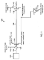
- Figure 1 shows an embodiment of an n-well voltage switching circuit 100 that is responsive to a mode control signal 105. If mode control signal 105 is asserted high (to indicate high-voltage mode operation), n-well voltage switching circuit 100 charges a switched n-well 110 for a dual-mode PMOS transistor 112 to a high voltage during a high-voltage (or power) mode of operation for dual-mode PMOS transistor 112. On the other hand, if mode control signal 105 is pulled low to select for a low-voltage mode of operation for dual-mode PMOS transistor 112, n-well voltage switching circuit 100 biases switched n-well 110 to a low voltage. In this fashion, switched n-well 110 need not be permanently tied to a high-voltage supply. As discussed further herein, dual-mode PMOS transistor 112 can then take advantage of the smaller dimensions (and thinner oxide) available in modern process nodes.
- An inverter 125 inverts mode control signal 105 into an inverted control signal 106.
- Inverted control signal 106 drives the gate of a native thick-oxide NMOS transistor 130.
- a drain of native thick-oxide NMOS transistor 130 is tied to a low voltage supply 120 whereas its source is tied to switched n-well 110.
- Low voltage supply 120 supplies the low voltage for switched n-well 110 when NMOS transistor 130 is turned on.
- mode control signal 105 goes low to select for a low-voltage mode of operation for dual-mode PMOS transistor 112
- inverted control signal 106 goes high such that NMOS transistor 130 turns fully on to bias switched n-well 110 to the low voltage.
- the source for NMOS transistor 130 forms part of an output node for n-well switching circuit 100 that couples to switched n-well 110.
- Inverted control signal 106 also drives the gate of a thick-oxide PMOS transistor 135, which is thus off in the low-voltage mode.
- the source of PMOS transistor 135 is tied to a high-voltage supply 115 and its drain is tied to switched n-well 110.
- mode control signal 105 is asserted high such that inverter 125 pulls inverted control signal 106 low so that PMOS transistor 135 is fully on.
- the drain of PMOS transistor 135 forms a remaining part of an output node for n-well voltage switching circuit 100 that couples to switched n-well 110.
- High-voltage supply 115 supplies the high voltage that biases switched n-well 110 when PMOS transistor 135 is turned on.
- NMOS transistor 130 is turned off in response to inverted control signal 106 going low at this time.
- switched n-well 110 for dual-mode PMOS transistor 112 is biased to the high voltage when mode control signal 105 goes high.
- PMOS transistor 135 is not stressed from the high voltage since its n-well 140 is also tied to high voltage supply 115 and because its gate oxide is relatively thick. In addition, PMOS transistor 135 has a size (channel length) sufficiently large to be robust to such a permanent coupling to the high voltage.
- control signal 106 should also be charged to the high voltage during the low-power mode of operation for dual-mode PMOS transistor 112. If control signal 106 were instead just charged to the low voltage during this time, the gate voltage of PMOS transistor 135 could be sufficiently lower than its source voltage so that PMOS transistor 135 would conduct rather than be shut off. Thus, high-voltage supply 115 supplies the power to inverter 125 so that control signal 106 is charged to the high voltage during the low-voltage mode of operation for dual-mode PMOS transistor 112. In this fashion, PMOS transistor 135 is fully off during the low-power mode of operation.
- NMOS transistor 130 is a thick-oxide transistor even though its drain is tied only to low-voltage supply 120 because its gate will thus be charged to the high voltage during the low-voltage mode of operation for dual-mode PMOS transistor 112.
- Both PMOS transistor 135 and NMOS transistor 130 must be relatively large and robust to withstand the strain from high-voltage supply 115. These transistors thus demand die space accordingly. But there need only be one n-well voltage switching circuit 100 to control the switched n-well potential for assorted other dual-mode PMOS transistors having the low and high voltage modes of operation. In this fashion, substantial die area savings may be realized.
- Dual-mode transistor PMOS 112 has a size that is smaller than the size used for PMOS transistor 135 and NMOS transistor 130. For example, dual-mode PMOS transistor 112 may have the minimum size and gate oxide thickness allowed by the process node. In this fashion, density is greatly enhanced.
- inverter 125 may be omitted in alternative embodiments in which control signal 105 is replaced with an active low control signal that would directly drive the gates of NMOS transistor 130 and PMOS transistor 135.
- the active low control signal would be pulled low to select for the high-voltage mode of operation.
- the active low control signal would be charged to the high voltage to select for the low-voltage mode of operation.
- an electrically-programmable fuse (e-fuse) memory includes assorted word line drivers as well as programming transistors.
- the corresponding transistors for the word line drivers and the associated programming transistors needed to be relatively large and have thick gate oxides to withstand the high voltage used to program the e-fuses.
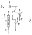
- an e-fuse memory 200 shown in Figure 2 enables the use of small thin-oxide word line drivers and programming transistors, which advantageously increases density.
- e-fuse memory 200 is shown with just a single word line 210 and a single bit line 225. It will be appreciated, however, that e-fuse memory 200 includes a plurality of other word lines and bit lines arranged analogously as shown for word line 210 and bit line 225. The other word lines would form additional rows in parallel with word line 210. Similarly, the other bit lines would form columns in parallel with bit line 225. When a word line is asserted by its word line driver, the corresponding e-fuses for that word line may be either read or programmed depending upon the bias for the bit lines. Each intersection of a word line and the bit lines corresponds to an e-fuse.
- an e-fuse 215 corresponds to the intersection of word line 210 and bit line 225.
- Each e-fuse comprises a fusible link that is conductive in the un-programmed state.
- a programmed e-fuse is either an open circuit or much more resistive as compared to an un-programmed e-fuse.
- To read a given e-fuse its word line and bit line are both asserted. Since an e-fuse should not be programmed in a read operation, the assertion of the word line and the bit line in a read operation may be performed using the low voltage. In contrast, the word line and bit line are both asserted to the high voltage to program a corresponding e-fuse. Reading the e-fuses would thus correspond to a low-voltage mode of operation whereas programming the e-fuses corresponds to a high-voltage mode of operation.
- a small thin-oxide word line (WL) driver PMOS transistor 205 has its drain tied to word line 210.
- WL driver PMOS transistor 205 has its switched n-well 110 controlled by n-well voltage switching circuit 100 as discussed with regard to Figure 1 .
- the source of WL driver PMOS transistor 205 is also tied to switched n-well 110 so that the voltage bias for both the source and switched n-well 110 are controlled by mode control signal 105.
- n-well voltage switching circuit 100 biases the source and switched n-well 110 for WL driver PMOS transistor 205 to the high voltage.
- a word line decoder (not illustrated) selects for word line 210 by pulling the gate of WL driver PMOS transistor 205 low.
- WL driver PMOS transistor 205 turns on and biases word line 210 to the high voltage.
- Word line 210 controls a gate of a small thin-oxide programming NMOS transistor 220 having its source tied to ground and a drain tied to a terminal of e-fuse 215. In the programming mode, programming NMOS transistor 220 thus has its gate biased to the high voltage.
- Bit line 225 couples to a remaining terminal of e-fuse 215. If bit line 225 is also charged to the high voltage when NMOS programming transistor 220 turns on, a relatively large amount of current will flow through e-fuse 215 so that it can be programmed.
- mode control signal 105 commands n-well voltage switching circuit 100 to bias the source and switched n-well 110 of WL driver PMOS transistor 205 to the low voltage. If the gate of WL driver PMOS transistor 205 is then pulled low, this transistor will then turn on to charge word line 210 to the low voltage so as to turn on NMOS programming transistor 220. During this read operation, bit line 225 is biased to the low-voltage. If e-fuse 215 is un-programmed, the assertion of word line 210 will pull the charged bit line 225 towards ground because of the conduction through NMOS programming transistor 220. In contrast, if e-fuse 215 had been programmed, bit line 225 will not be pulled to ground despite NMOS programming transistor 220 being turned on.
- WL driver PMOS transistor 205 is thus protected from latchup during the high-voltage mode of operation for programming e-fuses, it is not robust to a sufficiently long period of high-voltage operation since WL driver PMOS transistor 205 is a small thin-oxide transistor. But the programming of an e-fuse takes a relatively short amount of time as compared to the high-voltage longevity of such a small thin-oxide transistor.
- a controller 150 that controls the state of mode control signal 105 is configured to assert mode control signal 105 only for the relatively short amount of time necessary to program e-fuse 215.
- both WL driver PMOS transistor 205 and programming NMOS transistor 220 are biased by the high voltage only for the duration necessary to program e-fuse 215.
- both of these transistors can take advantage of the small dimensions and thin gate-oxide thickness available in modem process nodes, which greatly enhances die saving. For example, if memory 200 includes a plurality N of word lines and the same plurality N of bit lines, it would include N 2 e-fuses and would thus require N 2 programming transistors. The die area savings are thus quadratically related to the size of the memory.
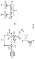
- n-well voltage switching discussed herein may also be applied to the power switch used to pull bit line 225 to the high voltage during the programming mode.
- a global power switch in series with a local power switch for the high-voltage charging of bit line 225.
- both these switches would comprise relatively large thick-oxide PMOS transistors having their n-wells permanently tied to high voltage supply 115 to prevent latchup.
- a local power switch comprises a relatively small thin-oxide PMOS transistor 300 having its switched n-well 110 controlled by n-well voltage switching circuit 100.
- a global power switch comprises a relatively large thick-oxide PMOS transistor 305 having its source and an un-switched n-well 306 tied to high-voltage supply 115.
- PMOS transistor 300 couples in series between bit line 225 and a drain for PMOS transistor 305.
- An enable programming control signal 315 is inverted through an inverter 310 to drive the gates of both PMOS transistors 305 and 300.
- enable programming control signal 315 is also the mode control signal for n-well voltage switching circuit 100.
- enable programming control signal 315 is asserted, switched n-well 110 is also charged to the high voltage.
- enable programming control signal 315 is de-asserted such that PMOS transistors 300 and 305 are turned off.
- n-well voltage switching circuit 100 biases switched n-well 110 to the low voltage. But note that a node 320 coupling to the source for PMOS transistor 300 was charged to the high voltage during the programming mode. To prevent any possibility of latchup occurring from this charged node potential as compared to the low voltage for switched n-well 110, an NMOS transistor 325 pulls node 320 to ground when memory 200 is not being programmed.
- inverter 310 drives the gate of NMOS transistor 325 such that NMOS transistor 325 turns on in response to the de-assertion of enable programming mode control signal 315.
- a source of NMOS transistor 325 is tied to ground whereas its drain is tied to node 320. In this fashion, NMOS transistor 325 will pull the potential for node 320 to ground when e-fuse memory 200 is not in the programming mode.
- a separate low voltage switch (not illustrated) would be active during a read mode of operation for memory 200 to charge bit line 225 to the low voltage.
- Electrically programmable memory 200 has numerous applications. For example, it conventional to use such a memory to configure a system-on-a-chip (SOC) with configuration data, trim data, RAM redundancy information, an encryption code, or other suitable information.
- Figure 4 illustrates some exemplary devices that include an SOC enhanced with electrically programmable memory 200.
- a cell phone 400, a laptop 405, and a tablet PC 410 may all include an electrically programmable memory 200 constructed in accordance with the disclosure.
- Other exemplary electronic systems such as a music player, a video player, a communication device, and a personal computer may also be configured with electrically programmable memories in accordance with the disclosure.
Description
- This application claims priority to
U.S. Nonprovisional Application No. 13/742,964, filed on January 16, 2013 - This application relates to integrated circuits, and more particularly to an n-well biasing scheme to prevent latchup for high-density applications.
- A PMOS transistor includes a p-type drain and source formed in an n-type body. Holes are thus the majority carrier in a PMOS channel. In complementary MOS (CMOS) technology, the bulk substrate is p-type such that the n-type body for a PMOS transistor exists as an n-type well (n-well) in the p-type substrate.
- Because holes are the majority carrier in a PMOS transistor, the PMOS source will be at a positive voltage with regard to the drain when the channel is conducting. This positive voltage on the source can be problematic in that a p-n junction is formed between the source and the n-well for the PMOS transistor. If the source is sufficiently biased with regard to the n-well, that p-n junction is then forward biased. A conducting parasitic structure results from this forward biased p-n junction and the ground connection to NMOS transistors in the p-type substrate. The resulting short circuit condition in the conducting parasitic structure is referred to as latchup. Latchup is dangerous in that the circuit can be destroyed from the latchup currents. Moreover, even if the circuit can withstand the short circuit currents, latchup inhibits normal operation.
- To prevent latchup, it is conventional to tie a PMOS transistor's n-well to the highest expected voltage. For example, if a PMOS transistor can operate in a low-voltage mode and also in a high-voltage mode, it is conventional to tie the PMOS n-well to the high-voltage supply used during the high-voltage mode operation. But the n-well tie is problematic as transistor dimensions are reduced such as in deep sub-micron technology. At these modem process nodes, the gate oxide is too thin and the transistor is too small to handle the stress resulting from tying the n-well to a relatively high-voltage supply.
- To solve the latchup problem for PMOS transistors in modem process nodes that can operate in both high and low voltage modes, it is conventional to use robust PMOS transistors. In other words, the transistor dimensions are increased and a relatively thick gate oxide is used. Such a large thick-gate oxide PMOS transistor can then have its n-well tied to the high-voltage supply without stressing the transistor. But the large transistor dimensions demand a lot of die area relative to the smaller transistor dimensions used in modern process nodes.
- Accordingly, there is a need in the art for latchup prevention architectures with increased density.
- Further attention is drawn to document
US 2005/200401 A1 which relates to an internal voltage generator which can restrict abnormal variations of an internal voltage resulting from a leakage current generated in a driving transistor. The internal voltage generator includes a comparator for receiving a reference voltage through its first input terminal, receiving the internal voltage through its second input terminal, and comparing the reference voltage with the internal voltage, a driving transistor for receiving the output signal from the comparator through its gate terminal, a first terminal of which being coupled to a driving voltage, a second terminal of which being an output terminal for outputting the internal voltage, a back bias circuit for supplying a predetermined potential of back bias voltage to a well region of the driving transistor, and a controller for receiving the output signal from the comparator, and controlling the operation of the back bias circuit. The second terminal of the driving transistor is feedback-coupled to the second input terminal of the comparator. When the driving transistor is turned off according to the output signal from the comparator, the controller for receiving the output signal from the comparator supplies the predetermined potential of back bias voltage to the well region of the driving transistor by driving the back bias circuit. - Furthermore attention is drawn to document "CIRCUIT SCHEME TO BIAS OCD OUTPUT STAGE N-WELL", IBM TECHNICAL DISCLOSURE BULLETIN, INTERNATIONAL BUSINESS MACHINES CORP. (THORNWOOD), US, vol. 34, no. 11, 1 APRIL 1992, pages 397-400, XP000303306, ISSN: 0018-8689.
- Finally, attention is drawn to document
US 6 452 858 B1 which relates to a semiconductor device to output voltages at three levels to a word driver while alleviating the breakdown voltage in the MOS transistor. The semiconductor is comprised of a breakdown-voltage reducing MOS transistor inserted in the word driver and two NMOS transistors to supply a read-out voltage to a word line. The word driver is moreover controlled by different voltage amplitudes on the main word lines and the common word lines. - In accordance with the present invention, a circuit as set forth in claim 1, and a method as set forth in claim 11, is provided. Further embodiments are claimed in the dependent claims. An n-well voltage switching circuit controls the voltage for a switched n-well of a dual-mode PMOS transistor to prevent latchup. The dual-mode PMOS transistor is controlled to operate in both a high-voltage mode and a low-voltage mode. In the high-voltage mode, the n-well voltage switching circuit biases the switched n-well to a high voltage. This high voltage is at least as high as any expected source (or drain) voltage for the dual-mode PMOS transistor during operation in the high-voltage mode. In this fashion, the p-n junction for the dual-mode PMOS transistor between its source and the switched n-well does not get forward biased and latchup is prevented accordingly.
- During the low-voltage mode of operation, the n-well voltage switching circuit biases the switched n-well to a low voltage that is lower than the high voltage. This low voltage is sufficiently low such that the dual-mode PMOS transistor is not strained during the low-voltage mode. In this fashion, the dual-mode PMOS transistor may be relatively small and have a thin-gate oxide to enhance density. A plurality of dual-mode PMOS transistors may have the voltage of their switched n-wells biased by the n-well voltage switching circuit to further enhance density.
- The n-well switching voltage switching circuit includes a first PMOS transistor of a first size having a first gate-oxide thickness. The first size and the first gate-oxide thickness have a magnitude such that a permanent coupling of an un-switched n-well and a source for the first PMOS transistor to a high-voltage supply providing the high voltage does not cause damage to the first PMOS transistor. In contrast, the dual-mode PMOS transistor has a second size that is less than the first size and a second gate-oxide thickness that is less than the first gate-oxide thickness. The second size and the second gate-oxide thickness have a magnitude such that the switched n-well for the dual-mode PMOS transistor cannot be permanently coupled to the high-voltage supply without incurring damage to the dual-mode PMOS transistor. To prevent such damage, the n-well voltage switching circuit is controlled so that the switched n-well is biased to the high voltage for no longer than a safe duration that protects the dual-mode PMOS transistor from damage despite its relatively small size and thin gate-oxide thickness.
-
-
Figure 1 is a schematic diagram for an n-well voltage switching circuit. -
Figure 2 is a schematic diagram for an electronically programmable memory incorporating the n-well voltage switching circuit ofFigure 1 . -
Figure 3 is a schematic diagram of a high voltage switch for the bit line in the memory ofFigure 2 . -
Figure 4 illustrates a plurality of electronic systems incorporating an electronically programmable memory in accordance with embodiments disclosed herein. - Embodiments of the present invention and their advantages are best understood by referring to the detailed description that follows. It should be appreciated that like reference numerals are used to identify like elements illustrated in one or more of the figures.
- To address the need in the art for latchup prevention architectures with increased density, an n-well voltage switching circuit is disclosed that controls the voltage bias for a dual-mode PMOS transistor's switched n-well. In a low-power mode of operation, the n-well voltage switching circuit biases the switched n-well to a relatively low voltage. Conversely, in a high-power mode of operation, the n-well voltage switching circuit biases the switched n-well to a relatively high voltage. What constitutes low and high voltage for the embodiments discussed herein depends upon the process node. For example, in a 20 nm process node, the high voltage may be 1.9 V whereas the low voltage may be 1 V. More generally, the high voltage has a magnitude that is too high for the switched n-well to be continuously biased to the high voltage without incurring damage to PMOS transistors within the n-well. In contrast, the low voltage is safe for a prolonged biasing of the switched n-well. What is safe versus what is not safe will depend on the particular process node being used.
- Turning now to the drawings,
Figure 1 shows an embodiment of an n-wellvoltage switching circuit 100 that is responsive to amode control signal 105. Ifmode control signal 105 is asserted high (to indicate high-voltage mode operation), n-wellvoltage switching circuit 100 charges a switched n-well 110 for a dual-mode PMOS transistor 112 to a high voltage during a high-voltage (or power) mode of operation for dual-mode PMOS transistor 112. On the other hand, ifmode control signal 105 is pulled low to select for a low-voltage mode of operation for dual-mode PMOS transistor 112, n-wellvoltage switching circuit 100 biases switched n-well 110 to a low voltage. In this fashion, switched n-well 110 need not be permanently tied to a high-voltage supply. As discussed further herein, dual-mode PMOS transistor 112 can then take advantage of the smaller dimensions (and thinner oxide) available in modern process nodes. - An
inverter 125 invertsmode control signal 105 into aninverted control signal 106.Inverted control signal 106 drives the gate of a native thick-oxide NMOS transistor 130. A drain of native thick-oxide NMOS transistor 130 is tied to alow voltage supply 120 whereas its source is tied to switched n-well 110.Low voltage supply 120 supplies the low voltage for switched n-well 110 whenNMOS transistor 130 is turned on. Thus, whenmode control signal 105 goes low to select for a low-voltage mode of operation for dual-mode PMOS transistor 112, invertedcontrol signal 106 goes high such thatNMOS transistor 130 turns fully on to bias switched n-well 110 to the low voltage. The source forNMOS transistor 130 forms part of an output node for n-well switching circuit 100 that couples to switched n-well 110.Inverted control signal 106 also drives the gate of a thick-oxide PMOS transistor 135, which is thus off in the low-voltage mode. The source ofPMOS transistor 135 is tied to a high-voltage supply 115 and its drain is tied to switched n-well 110. - To select for a high-voltage mode of operation,
mode control signal 105 is asserted high such thatinverter 125 pulls invertedcontrol signal 106 low so thatPMOS transistor 135 is fully on. The drain ofPMOS transistor 135 forms a remaining part of an output node for n-wellvoltage switching circuit 100 that couples to switched n-well 110. High-voltage supply 115 supplies the high voltage that biases switched n-well 110 whenPMOS transistor 135 is turned on.NMOS transistor 130 is turned off in response toinverted control signal 106 going low at this time. Thus, switched n-well 110 for dual-mode PMOS transistor 112 is biased to the high voltage whenmode control signal 105 goes high.PMOS transistor 135 is not stressed from the high voltage since its n-well 140 is also tied tohigh voltage supply 115 and because its gate oxide is relatively thick. In addition,PMOS transistor 135 has a size (channel length) sufficiently large to be robust to such a permanent coupling to the high voltage. - Because the source of
PMOS transistor 135 is tied tohigh voltage supply 115,control signal 106 should also be charged to the high voltage during the low-power mode of operation for dual-mode PMOS transistor 112. Ifcontrol signal 106 were instead just charged to the low voltage during this time, the gate voltage ofPMOS transistor 135 could be sufficiently lower than its source voltage so thatPMOS transistor 135 would conduct rather than be shut off. Thus, high-voltage supply 115 supplies the power to inverter 125 so thatcontrol signal 106 is charged to the high voltage during the low-voltage mode of operation for dual-mode PMOS transistor 112. In this fashion,PMOS transistor 135 is fully off during the low-power mode of operation.NMOS transistor 130 is a thick-oxide transistor even though its drain is tied only to low-voltage supply 120 because its gate will thus be charged to the high voltage during the low-voltage mode of operation for dual-mode PMOS transistor 112. - Both
PMOS transistor 135 andNMOS transistor 130 must be relatively large and robust to withstand the strain from high-voltage supply 115. These transistors thus demand die space accordingly. But there need only be one n-wellvoltage switching circuit 100 to control the switched n-well potential for assorted other dual-mode PMOS transistors having the low and high voltage modes of operation. In this fashion, substantial die area savings may be realized. Dual-mode transistor PMOS 112 has a size that is smaller than the size used forPMOS transistor 135 andNMOS transistor 130. For example, dual-mode PMOS transistor 112 may have the minimum size and gate oxide thickness allowed by the process node. In this fashion, density is greatly enhanced. - It will be appreciated that
inverter 125 may be omitted in alternative embodiments in which control signal 105 is replaced with an active low control signal that would directly drive the gates ofNMOS transistor 130 andPMOS transistor 135. In such an embodiment, the active low control signal would be pulled low to select for the high-voltage mode of operation. Conversely, the active low control signal would be charged to the high voltage to select for the low-voltage mode of operation. - Numerous applications may advantageously use relatively small thin-oxide dual-mode PMOS transistors in switched n-wells disclosed herein. For example, an electrically-programmable fuse (e-fuse) memory includes assorted word line drivers as well as programming transistors. In a conventional e-fuse memory, the corresponding transistors for the word line drivers and the associated programming transistors needed to be relatively large and have thick gate oxides to withstand the high voltage used to program the e-fuses. In contrast, an
e-fuse memory 200 shown inFigure 2 enables the use of small thin-oxide word line drivers and programming transistors, which advantageously increases density. - For illustration clarity,
e-fuse memory 200 is shown with just asingle word line 210 and asingle bit line 225. It will be appreciated, however, thate-fuse memory 200 includes a plurality of other word lines and bit lines arranged analogously as shown forword line 210 andbit line 225. The other word lines would form additional rows in parallel withword line 210. Similarly, the other bit lines would form columns in parallel withbit line 225. When a word line is asserted by its word line driver, the corresponding e-fuses for that word line may be either read or programmed depending upon the bias for the bit lines. Each intersection of a word line and the bit lines corresponds to an e-fuse. For example, an e-fuse 215 corresponds to the intersection ofword line 210 andbit line 225. Each e-fuse comprises a fusible link that is conductive in the un-programmed state. In contrast, a programmed e-fuse is either an open circuit or much more resistive as compared to an un-programmed e-fuse. To read a given e-fuse, its word line and bit line are both asserted. Since an e-fuse should not be programmed in a read operation, the assertion of the word line and the bit line in a read operation may be performed using the low voltage. In contrast, the word line and bit line are both asserted to the high voltage to program a corresponding e-fuse. Reading the e-fuses would thus correspond to a low-voltage mode of operation whereas programming the e-fuses corresponds to a high-voltage mode of operation. - Given these low and high voltage modes of operation, the word line driver transistors may thus be advantageously implemented using a switched n-well so that these transistors may remain relatively small yet be robust to the high-voltage mode of operation. With regard to
e-fuse 215, a small thin-oxide word line (WL)driver PMOS transistor 205 has its drain tied toword line 210. WLdriver PMOS transistor 205 has its switched n-well 110 controlled by n-wellvoltage switching circuit 100 as discussed with regard toFigure 1 . In addition, the source of WLdriver PMOS transistor 205 is also tied to switched n-well 110 so that the voltage bias for both the source and switched n-well 110 are controlled bymode control signal 105. Thus, ife-fuse 215 is to be programmed, n-wellvoltage switching circuit 100 biases the source and switched n-well 110 for WLdriver PMOS transistor 205 to the high voltage. A word line decoder (not illustrated) selects forword line 210 by pulling the gate of WLdriver PMOS transistor 205 low. In response, WLdriver PMOS transistor 205 turns on andbiases word line 210 to the high voltage.Word line 210 controls a gate of a small thin-oxideprogramming NMOS transistor 220 having its source tied to ground and a drain tied to a terminal ofe-fuse 215. In the programming mode,programming NMOS transistor 220 thus has its gate biased to the high voltage.Bit line 225 couples to a remaining terminal ofe-fuse 215. Ifbit line 225 is also charged to the high voltage whenNMOS programming transistor 220 turns on, a relatively large amount of current will flow throughe-fuse 215 so that it can be programmed. - To read the state of
e-fuse 215,mode control signal 105 commands n-wellvoltage switching circuit 100 to bias the source and switched n-well 110 of WLdriver PMOS transistor 205 to the low voltage. If the gate of WLdriver PMOS transistor 205 is then pulled low, this transistor will then turn on to chargeword line 210 to the low voltage so as to turn onNMOS programming transistor 220. During this read operation,bit line 225 is biased to the low-voltage. Ife-fuse 215 is un-programmed, the assertion ofword line 210 will pull the chargedbit line 225 towards ground because of the conduction throughNMOS programming transistor 220. In contrast, ife-fuse 215 had been programmed,bit line 225 will not be pulled to ground despiteNMOS programming transistor 220 being turned on. - Although WL
driver PMOS transistor 205 is thus protected from latchup during the high-voltage mode of operation for programming e-fuses, it is not robust to a sufficiently long period of high-voltage operation since WLdriver PMOS transistor 205 is a small thin-oxide transistor. But the programming of an e-fuse takes a relatively short amount of time as compared to the high-voltage longevity of such a small thin-oxide transistor. Referring back toFigure 1 , acontroller 150 that controls the state ofmode control signal 105 is configured to assertmode control signal 105 only for the relatively short amount of time necessary to program e-fuse 215. In this fashion, both WLdriver PMOS transistor 205 andprogramming NMOS transistor 220 are biased by the high voltage only for the duration necessary to program e-fuse 215. Thus, both of these transistors can take advantage of the small dimensions and thin gate-oxide thickness available in modem process nodes, which greatly enhances die saving. For example, ifmemory 200 includes a plurality N of word lines and the same plurality N of bit lines, it would include N2 e-fuses and would thus require N2 programming transistors. The die area savings are thus quadratically related to the size of the memory. - The n-well voltage switching discussed herein may also be applied to the power switch used to pull
bit line 225 to the high voltage during the programming mode. In that regard, it is advantageous to include a global power switch in series with a local power switch for the high-voltage charging ofbit line 225. In a conventional e-fuse memory, both these switches would comprise relatively large thick-oxide PMOS transistors having their n-wells permanently tied tohigh voltage supply 115 to prevent latchup. But as shown inFigure 3 , a local power switch comprises a relatively small thin-oxide PMOS transistor 300 having its switched n-well 110 controlled by n-wellvoltage switching circuit 100. A global power switch comprises a relatively large thick-oxide PMOS transistor 305 having its source and an un-switched n-well 306 tied to high-voltage supply 115.PMOS transistor 300 couples in series betweenbit line 225 and a drain forPMOS transistor 305. An enableprogramming control signal 315 is inverted through aninverter 310 to drive the gates of bothPMOS transistors programming control signal 315 is asserted high to select for the programming mode fore-fuse 215,PMOS transistors bit line 225 is charged to the high voltage from high voltage. In this embodiment, enableprogramming control signal 315 is also the mode control signal for n-wellvoltage switching circuit 100. Thus, when enableprogramming control signal 315 is asserted, switched n-well 110 is also charged to the high voltage. - After e-fuse 215 has been programmed, enable
programming control signal 315 is de-asserted such thatPMOS transistors voltage switching circuit 100 biases switched n-well 110 to the low voltage. But note that anode 320 coupling to the source forPMOS transistor 300 was charged to the high voltage during the programming mode. To prevent any possibility of latchup occurring from this charged node potential as compared to the low voltage for switched n-well 110, anNMOS transistor 325 pullsnode 320 to ground whenmemory 200 is not being programmed. To do so,inverter 310 drives the gate ofNMOS transistor 325 such thatNMOS transistor 325 turns on in response to the de-assertion of enable programmingmode control signal 315. A source ofNMOS transistor 325 is tied to ground whereas its drain is tied tonode 320. In this fashion,NMOS transistor 325 will pull the potential fornode 320 to ground whene-fuse memory 200 is not in the programming mode. A separate low voltage switch (not illustrated) would be active during a read mode of operation formemory 200 to chargebit line 225 to the low voltage. - Electrically
programmable memory 200 has numerous applications. For example, it conventional to use such a memory to configure a system-on-a-chip (SOC) with configuration data, trim data, RAM redundancy information, an encryption code, or other suitable information.Figure 4 illustrates some exemplary devices that include an SOC enhanced with electricallyprogrammable memory 200. In particular, acell phone 400, alaptop 405, and atablet PC 410 may all include an electricallyprogrammable memory 200 constructed in accordance with the disclosure. Other exemplary electronic systems such as a music player, a video player, a communication device, and a personal computer may also be configured with electrically programmable memories in accordance with the disclosure. - As those of some skill in this art will by now appreciate and depending on the particular application at hand, many modifications, substitutions and variations can be made in and to the materials, apparatus, configurations and methods of use of the devices of the present disclosure without departing from the scope thereof. In light of this, the scope of the present disclosure should not be limited to that of the particular embodiments illustrated and described herein, as they are merely by way of some examples thereof, but rather, should be fully commensurate with that of the claims appended hereafter.
Claims (15)
- A circuit, comprising:a thin-oxide PMOS transistor (112) having a source and a switched n-well (110);a native thick-oxide NMOS transistor (130) having a gate controlled responsive to a control signal, a drain coupled to a low-voltage supply (120) configured to provide a low voltage, and a source coupled to the thin-oxide PMOS transistor's source and switched n-well (110); anda thick-oxide PMOS transistor (135) having a gate controlled responsive to the control signal, a source coupled to a high-voltage supply (115) configured to provide a high voltage that is greater than the low voltage, and a drain coupled to the thin-oxide PMOS transistor's source and switched n-well (110), wherein the native thick-oxide NMOS transistor (130) and the thick-oxide PMOS transistor (135) each have a first gate-oxide thickness that is greater than a second gate-oxide thickness for the thin-oxide PMOS transistor (112).
- The circuit of claim 1, further comprising an inverter (125) configured to invert the control signal into an inverted control signal, and wherein the gate for the native thick-oxide NMOS transistor (130) and the gate for the thick-oxide PMOS transistor (135) are configured to be driven by the inverted control signal.
- The circuit of claim 2, wherein the thick-oxide PMOS transistor (135) includes an un-switched n-well (140) permanently coupled to the high-voltage supply (115).
- The circuit of claim 3, wherein the thick-oxide PMOS transistor (135) has a first size and wherein the thin-oxide PMOS transistor (112) has a second size smaller than the first size.
- The circuit of claim 4, wherein the first size and the first gate-oxide thickness each have a magnitude sufficient to protect the thick-oxide PMOS transistor (135) from its un-switched n-well (140) being permanently coupled to the high-voltage supply (115).
- The circuit of claim 4, wherein the second size and the second gate-oxide thickness each have a magnitude that is not sufficient to protect the thin-oxide PMOS transistor from a permanent tie of the high-voltage supply to the switched n-well.
- The circuit of claim 4, further comprising:a memory, wherein the thin-oxide PMOS transistor is a word line driver transistor (205) for the memory.
- The memory circuit of claim 7, wherein the memory is an electrical programmable memory further comprising an e-fuse (215) having a terminal coupled to a drain of a thin gate-oxide programming NMOS transistor, the thin gate-oxide programming NMOS transistor having its gate coupled to a word line (220), the word line (220) being coupled to a drain for the word line driver PMOS transistor (205).
- The memory circuit of claim 8, further comprising a bit line (225) coupled to an opposing terminal of the e-fuse (215).
- The memory circuit of claim 9, further comprising a high power switch for biasing the bit line (225) to the high voltage during a programming mode for the e-fuse (215), wherein the high power switch includes a global power switch and a local power switch in series between the bit line and a high voltage supply configured to supply the high voltage.
- A method, comprising:responsive to receiving a control signal in a first state at an n-well voltage switching circuit (100), biasing both a source and a switched n-well of a thin-oxide PMOS transistor (112) with a first voltage, wherein the n-well voltage switching circuit (100) comprises transistors of a first size and a first gate-oxide thickness, and wherein the thin-oxide PMOS transistor (112) has a second size that is less than the first size and a second gate-oxide thickness that is less than the first gate-oxide thickness, andresponsive to receiving the control signal in a second state at the n-well voltage switching circuit (100), biasing the switched n-well with a second voltage that is less than the first voltage.
- The method of claim 11, wherein the second gate-oxide thickness is not sufficient to prevent the thin-oxide PMOS transistor (112) from damage from a permanent bias of the switched n-well to the first voltage, further comprising limiting a duration for the receipt of the control signal in the first state such that the thin-oxide PMOS transistor (112) is not damaged by the bias of its switched n-well with the first voltage.
- The method of claim 11, wherein the thin-oxide PMOS transistor (112) is a word line driver transistor (205) for an electrically programmable memory, and wherein biasing the switched n-well with the first voltage comprises programming an e-fuse (215) through the word line driver transistor (205).
- The method of claim 13, wherein biasing the switched n-well with the second voltage comprises reading a state of the e-fuse.
- The method of claim 13, further comprising biasing a bit line coupled to the e-fuse to the high voltage during the programming of the e-fuse, wherein biasing the bit line comprises biasing the bit line through a local power switch PMOS transistor having a switched n-well biased by the n-well voltage switching circuit to the second voltage.
Applications Claiming Priority (2)
| Application Number | Priority Date | Filing Date | Title |
|---|---|---|---|
| US13/742,964 US8787096B1 (en) | 2013-01-16 | 2013-01-16 | N-well switching circuit |
| PCT/US2014/011138 WO2014113295A1 (en) | 2013-01-16 | 2014-01-10 | N-well switching circuit |
Publications (2)
| Publication Number | Publication Date |
|---|---|
| EP2946474A1 EP2946474A1 (en) | 2015-11-25 |
| EP2946474B1 true EP2946474B1 (en) | 2016-07-27 |
Family
ID=50031588
Family Applications (1)
| Application Number | Title | Priority Date | Filing Date |
|---|---|---|---|
| EP14702369.1A Not-in-force EP2946474B1 (en) | 2013-01-16 | 2014-01-10 | N-well switching circuit |
Country Status (6)
| Country | Link |
|---|---|
| US (2) | US8787096B1 (en) |
| EP (1) | EP2946474B1 (en) |
| JP (1) | JP6092427B2 (en) |
| KR (1) | KR101557812B1 (en) |
| CN (1) | CN104937848B (en) |
| WO (1) | WO2014113295A1 (en) |
Families Citing this family (11)
| Publication number | Priority date | Publication date | Assignee | Title |
|---|---|---|---|---|
| US8787096B1 (en) | 2013-01-16 | 2014-07-22 | Qualcomm Incorporated | N-well switching circuit |
| US9082498B2 (en) * | 2013-08-08 | 2015-07-14 | Qualcomm Incorporated | N-well switching circuit |
| US10131884B2 (en) | 2015-02-23 | 2018-11-20 | Lanzatech New Zealand Limited | Recombinant acetogenic bacterium for the conversion of methane to products |
| CN105049029B (en) * | 2015-07-06 | 2018-05-04 | 上海巨微集成电路有限公司 | A kind of PMOS tube substrate switching circuit |
| BR112018007338A2 (en) | 2015-10-13 | 2018-10-23 | Lanzatech New Zealand Ltd | genetically engineered and modified bacteria, and method for producing a product |
| EP3981869A1 (en) | 2015-12-03 | 2022-04-13 | LanzaTech NZ, Inc. | Arginine as sole nitrogen source for c1-fixing microorganism |
| FI3411489T3 (en) | 2016-02-01 | 2023-08-23 | Lanzatech Nz Inc | Integrated fermentation and electrolysis process |
| CN114908093A (en) | 2016-02-26 | 2022-08-16 | 朗泽科技新西兰有限公司 | CRISPR/CAS system for C1 immobilized bacteria |
| US9570192B1 (en) | 2016-03-04 | 2017-02-14 | Qualcomm Incorporated | System and method for reducing programming voltage stress on memory cell devices |
| CN111683731B (en) | 2018-02-12 | 2022-09-02 | 朗泽科技有限公司 | Process for improving carbon conversion efficiency |
| ES2960999T3 (en) | 2018-04-20 | 2024-03-07 | Lanzatech Inc | Fermentation process to produce ethanol |
Family Cites Families (22)
| Publication number | Priority date | Publication date | Assignee | Title |
|---|---|---|---|---|
| US4670668A (en) | 1985-05-09 | 1987-06-02 | Advanced Micro Devices, Inc. | Substrate bias generator with power supply control means to sequence application of bias and power to prevent CMOS SCR latch-up |
| KR0169157B1 (en) * | 1993-11-29 | 1999-02-01 | 기다오까 다까시 | Semiconductor circuit and mos-dram |
| JP3264622B2 (en) | 1996-07-16 | 2002-03-11 | 株式会社東芝 | Semiconductor device |
| US5844425A (en) | 1996-07-19 | 1998-12-01 | Quality Semiconductor, Inc. | CMOS tristate output buffer with having overvoltage protection and increased stability against bus voltage variations |
| TW453032B (en) * | 1998-09-09 | 2001-09-01 | Hitachi Ltd | Semiconductor integrated circuit apparatus |
| JP4105833B2 (en) * | 1998-09-09 | 2008-06-25 | 株式会社ルネサステクノロジ | Semiconductor integrated circuit device |
| US6452858B1 (en) * | 1999-11-05 | 2002-09-17 | Hitachi, Ltd. | Semiconductor device |
| US6377112B1 (en) | 2000-12-05 | 2002-04-23 | Semiconductor Components Industries Llc | Circuit and method for PMOS device N-well bias control |
| US6573134B2 (en) * | 2001-03-27 | 2003-06-03 | Sharp Laboratories Of America, Inc. | Dual metal gate CMOS devices and method for making the same |
| US7218151B1 (en) * | 2002-06-28 | 2007-05-15 | University Of Rochester | Domino logic with variable threshold voltage keeper |
| US6882188B1 (en) * | 2003-09-30 | 2005-04-19 | Faraday Technology Corp. | Input/output buffer |
| US7038274B2 (en) * | 2003-11-13 | 2006-05-02 | Volterra Semiconductor Corporation | Switching regulator with high-side p-type device |
| US7046493B2 (en) * | 2003-12-12 | 2006-05-16 | Faraday Technology Corp. | Input/output buffer protection circuit |
| KR100728950B1 (en) * | 2004-03-11 | 2007-06-15 | 주식회사 하이닉스반도체 | An internal voltage generator |
| FR2894373B1 (en) * | 2005-12-07 | 2008-01-04 | Atmel Corp | AUTONOMOUS ANTI-FUSE CELL |
| US7355437B2 (en) * | 2006-03-06 | 2008-04-08 | Altera Corporation | Latch-up prevention circuitry for integrated circuits with transistor body biasing |
| US7330049B2 (en) * | 2006-03-06 | 2008-02-12 | Altera Corporation | Adjustable transistor body bias generation circuitry with latch-up prevention |
| TWI451697B (en) * | 2006-05-03 | 2014-09-01 | Synopsys Inc | Very low power analog compensation circuit |
| US7863962B2 (en) * | 2008-04-17 | 2011-01-04 | National Semiconductor Corporation | High voltage CMOS output buffer constructed from low voltage CMOS transistors |
| US7800179B2 (en) * | 2009-02-04 | 2010-09-21 | Fairchild Semiconductor Corporation | High speed, low power consumption, isolated analog CMOS unit |
| CN101997305B (en) | 2009-08-26 | 2013-04-10 | 安凯(广州)微电子技术有限公司 | Reverse voltage protection circuit and power tube device |
| US8787096B1 (en) | 2013-01-16 | 2014-07-22 | Qualcomm Incorporated | N-well switching circuit |
-
2013
- 2013-01-16 US US13/742,964 patent/US8787096B1/en active Active
-
2014
- 2014-01-10 KR KR1020157021577A patent/KR101557812B1/en active IP Right Grant
- 2014-01-10 EP EP14702369.1A patent/EP2946474B1/en not_active Not-in-force
- 2014-01-10 JP JP2015552832A patent/JP6092427B2/en not_active Expired - Fee Related
- 2014-01-10 WO PCT/US2014/011138 patent/WO2014113295A1/en active Application Filing
- 2014-01-10 CN CN201480004776.9A patent/CN104937848B/en active Active
- 2014-08-29 US US14/472,953 patent/US9252765B2/en active Active
Also Published As
| Publication number | Publication date |
|---|---|
| CN104937848B (en) | 2017-12-05 |
| WO2014113295A1 (en) | 2014-07-24 |
| KR20150097815A (en) | 2015-08-26 |
| JP2016511933A (en) | 2016-04-21 |
| US20140369152A1 (en) | 2014-12-18 |
| EP2946474A1 (en) | 2015-11-25 |
| JP6092427B2 (en) | 2017-03-08 |
| KR101557812B1 (en) | 2015-10-06 |
| US8787096B1 (en) | 2014-07-22 |
| CN104937848A (en) | 2015-09-23 |
| US20140198588A1 (en) | 2014-07-17 |
| US9252765B2 (en) | 2016-02-02 |
Similar Documents
| Publication | Publication Date | Title |
|---|---|---|
| EP2946474B1 (en) | N-well switching circuit | |
| JP2016511933A5 (en) | ||
| US7224630B2 (en) | Antifuse circuit | |
| US10305474B2 (en) | High voltage output driver with low voltage devices | |
| US8184489B2 (en) | Level shifting circuit | |
| US9748957B2 (en) | Voltage level shifter circuit, system, and method for wide supply voltage applications | |
| TW201616274A (en) | Semiconductor device | |
| US9082498B2 (en) | N-well switching circuit | |
| US20090295447A1 (en) | Apparatus and methods for a high-voltage latch | |
| US7764108B2 (en) | Electrical fuse circuit | |
| US20120081165A1 (en) | High voltage tolerative driver | |
| US9780030B2 (en) | Integrated circuit | |
| US11205488B2 (en) | Apparatuses and methods for transistor protection by charge sharing | |
| US7379358B2 (en) | Repair I/O fuse circuit of semiconductor memory device | |
| US20090052102A1 (en) | Semiconductor device | |
| US8787109B2 (en) | Word line driver having a control switch | |
| US11176985B1 (en) | Boundary protection in memory | |
| US11726539B2 (en) | Power management circuit, system-on-chip device, and method of power management | |
| KR100924341B1 (en) | Latch Circuit | |
| KR20150093079A (en) | Semiconductor device |
Legal Events
| Date | Code | Title | Description |
|---|---|---|---|
| PUAI | Public reference made under article 153(3) epc to a published international application that has entered the european phase |
Free format text: ORIGINAL CODE: 0009012 |
|
| 17P | Request for examination filed |
Effective date: 20150717 |
|
| AK | Designated contracting states |
Kind code of ref document: A1 Designated state(s): AL AT BE BG CH CY CZ DE DK EE ES FI FR GB GR HR HU IE IS IT LI LT LU LV MC MK MT NL NO PL PT RO RS SE SI SK SM TR |
|
| AX | Request for extension of the european patent |
Extension state: BA ME |
|
| GRAP | Despatch of communication of intention to grant a patent |
Free format text: ORIGINAL CODE: EPIDOSNIGR1 |
|
| DAX | Request for extension of the european patent (deleted) | ||
| INTG | Intention to grant announced |
Effective date: 20160210 |
|
| GRAS | Grant fee paid |
Free format text: ORIGINAL CODE: EPIDOSNIGR3 |
|
| GRAA | (expected) grant |
Free format text: ORIGINAL CODE: 0009210 |
|
| AK | Designated contracting states |
Kind code of ref document: B1 Designated state(s): AL AT BE BG CH CY CZ DE DK EE ES FI FR GB GR HR HU IE IS IT LI LT LU LV MC MK MT NL NO PL PT RO RS SE SI SK SM TR |
|
| REG | Reference to a national code |
Ref country code: GB Ref legal event code: FG4D |
|
| REG | Reference to a national code |
Ref country code: CH Ref legal event code: EP |
|
| REG | Reference to a national code |
Ref country code: FR Ref legal event code: PLFP Year of fee payment: 4 |
|
| REG | Reference to a national code |
Ref country code: AT Ref legal event code: REF Ref document number: 816518 Country of ref document: AT Kind code of ref document: T Effective date: 20160815 |
|
| REG | Reference to a national code |
Ref country code: IE Ref legal event code: FG4D |
|
| REG | Reference to a national code |
Ref country code: DE Ref legal event code: R096 Ref document number: 602014002896 Country of ref document: DE |
|
| REG | Reference to a national code |
Ref country code: LT Ref legal event code: MG4D |
|
| REG | Reference to a national code |
Ref country code: NL Ref legal event code: MP Effective date: 20160727 |
|
| REG | Reference to a national code |
Ref country code: AT Ref legal event code: MK05 Ref document number: 816518 Country of ref document: AT Kind code of ref document: T Effective date: 20160727 |
|
| PG25 | Lapsed in a contracting state [announced via postgrant information from national office to epo] |
Ref country code: LT Free format text: LAPSE BECAUSE OF FAILURE TO SUBMIT A TRANSLATION OF THE DESCRIPTION OR TO PAY THE FEE WITHIN THE PRESCRIBED TIME-LIMIT Effective date: 20160727 Ref country code: NL Free format text: LAPSE BECAUSE OF FAILURE TO SUBMIT A TRANSLATION OF THE DESCRIPTION OR TO PAY THE FEE WITHIN THE PRESCRIBED TIME-LIMIT Effective date: 20160727 Ref country code: IT Free format text: LAPSE BECAUSE OF FAILURE TO SUBMIT A TRANSLATION OF THE DESCRIPTION OR TO PAY THE FEE WITHIN THE PRESCRIBED TIME-LIMIT Effective date: 20160727 Ref country code: NO Free format text: LAPSE BECAUSE OF FAILURE TO SUBMIT A TRANSLATION OF THE DESCRIPTION OR TO PAY THE FEE WITHIN THE PRESCRIBED TIME-LIMIT Effective date: 20161027 Ref country code: FI Free format text: LAPSE BECAUSE OF FAILURE TO SUBMIT A TRANSLATION OF THE DESCRIPTION OR TO PAY THE FEE WITHIN THE PRESCRIBED TIME-LIMIT Effective date: 20160727 Ref country code: IS Free format text: LAPSE BECAUSE OF FAILURE TO SUBMIT A TRANSLATION OF THE DESCRIPTION OR TO PAY THE FEE WITHIN THE PRESCRIBED TIME-LIMIT Effective date: 20161127 Ref country code: HR Free format text: LAPSE BECAUSE OF FAILURE TO SUBMIT A TRANSLATION OF THE DESCRIPTION OR TO PAY THE FEE WITHIN THE PRESCRIBED TIME-LIMIT Effective date: 20160727 Ref country code: RS Free format text: LAPSE BECAUSE OF FAILURE TO SUBMIT A TRANSLATION OF THE DESCRIPTION OR TO PAY THE FEE WITHIN THE PRESCRIBED TIME-LIMIT Effective date: 20160727 |
|
| PG25 | Lapsed in a contracting state [announced via postgrant information from national office to epo] |
Ref country code: ES Free format text: LAPSE BECAUSE OF FAILURE TO SUBMIT A TRANSLATION OF THE DESCRIPTION OR TO PAY THE FEE WITHIN THE PRESCRIBED TIME-LIMIT Effective date: 20160727 Ref country code: LV Free format text: LAPSE BECAUSE OF FAILURE TO SUBMIT A TRANSLATION OF THE DESCRIPTION OR TO PAY THE FEE WITHIN THE PRESCRIBED TIME-LIMIT Effective date: 20160727 Ref country code: AT Free format text: LAPSE BECAUSE OF FAILURE TO SUBMIT A TRANSLATION OF THE DESCRIPTION OR TO PAY THE FEE WITHIN THE PRESCRIBED TIME-LIMIT Effective date: 20160727 Ref country code: PL Free format text: LAPSE BECAUSE OF FAILURE TO SUBMIT A TRANSLATION OF THE DESCRIPTION OR TO PAY THE FEE WITHIN THE PRESCRIBED TIME-LIMIT Effective date: 20160727 Ref country code: GR Free format text: LAPSE BECAUSE OF FAILURE TO SUBMIT A TRANSLATION OF THE DESCRIPTION OR TO PAY THE FEE WITHIN THE PRESCRIBED TIME-LIMIT Effective date: 20161028 Ref country code: BE Free format text: LAPSE BECAUSE OF FAILURE TO SUBMIT A TRANSLATION OF THE DESCRIPTION OR TO PAY THE FEE WITHIN THE PRESCRIBED TIME-LIMIT Effective date: 20160727 Ref country code: SE Free format text: LAPSE BECAUSE OF FAILURE TO SUBMIT A TRANSLATION OF THE DESCRIPTION OR TO PAY THE FEE WITHIN THE PRESCRIBED TIME-LIMIT Effective date: 20160727 Ref country code: PT Free format text: LAPSE BECAUSE OF FAILURE TO SUBMIT A TRANSLATION OF THE DESCRIPTION OR TO PAY THE FEE WITHIN THE PRESCRIBED TIME-LIMIT Effective date: 20161128 |
|
| PG25 | Lapsed in a contracting state [announced via postgrant information from national office to epo] |
Ref country code: RO Free format text: LAPSE BECAUSE OF FAILURE TO SUBMIT A TRANSLATION OF THE DESCRIPTION OR TO PAY THE FEE WITHIN THE PRESCRIBED TIME-LIMIT Effective date: 20160727 Ref country code: EE Free format text: LAPSE BECAUSE OF FAILURE TO SUBMIT A TRANSLATION OF THE DESCRIPTION OR TO PAY THE FEE WITHIN THE PRESCRIBED TIME-LIMIT Effective date: 20160727 |
|
| REG | Reference to a national code |
Ref country code: DE Ref legal event code: R097 Ref document number: 602014002896 Country of ref document: DE |
|
| PG25 | Lapsed in a contracting state [announced via postgrant information from national office to epo] |
Ref country code: CZ Free format text: LAPSE BECAUSE OF FAILURE TO SUBMIT A TRANSLATION OF THE DESCRIPTION OR TO PAY THE FEE WITHIN THE PRESCRIBED TIME-LIMIT Effective date: 20160727 Ref country code: SM Free format text: LAPSE BECAUSE OF FAILURE TO SUBMIT A TRANSLATION OF THE DESCRIPTION OR TO PAY THE FEE WITHIN THE PRESCRIBED TIME-LIMIT Effective date: 20160727 Ref country code: SK Free format text: LAPSE BECAUSE OF FAILURE TO SUBMIT A TRANSLATION OF THE DESCRIPTION OR TO PAY THE FEE WITHIN THE PRESCRIBED TIME-LIMIT Effective date: 20160727 Ref country code: BG Free format text: LAPSE BECAUSE OF FAILURE TO SUBMIT A TRANSLATION OF THE DESCRIPTION OR TO PAY THE FEE WITHIN THE PRESCRIBED TIME-LIMIT Effective date: 20161027 Ref country code: DK Free format text: LAPSE BECAUSE OF FAILURE TO SUBMIT A TRANSLATION OF THE DESCRIPTION OR TO PAY THE FEE WITHIN THE PRESCRIBED TIME-LIMIT Effective date: 20160727 |
|
| PLBE | No opposition filed within time limit |
Free format text: ORIGINAL CODE: 0009261 |
|
| STAA | Information on the status of an ep patent application or granted ep patent |
Free format text: STATUS: NO OPPOSITION FILED WITHIN TIME LIMIT |
|
| 26N | No opposition filed |
Effective date: 20170502 |
|
| PG25 | Lapsed in a contracting state [announced via postgrant information from national office to epo] |
Ref country code: SI Free format text: LAPSE BECAUSE OF FAILURE TO SUBMIT A TRANSLATION OF THE DESCRIPTION OR TO PAY THE FEE WITHIN THE PRESCRIBED TIME-LIMIT Effective date: 20160727 |
|
| REG | Reference to a national code |
Ref country code: CH Ref legal event code: PL |
|
| PG25 | Lapsed in a contracting state [announced via postgrant information from national office to epo] |
Ref country code: MC Free format text: LAPSE BECAUSE OF FAILURE TO SUBMIT A TRANSLATION OF THE DESCRIPTION OR TO PAY THE FEE WITHIN THE PRESCRIBED TIME-LIMIT Effective date: 20160727 |
|
| PG25 | Lapsed in a contracting state [announced via postgrant information from national office to epo] |
Ref country code: LI Free format text: LAPSE BECAUSE OF NON-PAYMENT OF DUE FEES Effective date: 20170131 Ref country code: CH Free format text: LAPSE BECAUSE OF NON-PAYMENT OF DUE FEES Effective date: 20170131 |
|
| REG | Reference to a national code |
Ref country code: IE Ref legal event code: MM4A |
|
| PG25 | Lapsed in a contracting state [announced via postgrant information from national office to epo] |
Ref country code: LU Free format text: LAPSE BECAUSE OF NON-PAYMENT OF DUE FEES Effective date: 20170110 |
|
| REG | Reference to a national code |
Ref country code: FR Ref legal event code: PLFP Year of fee payment: 5 |
|
| PG25 | Lapsed in a contracting state [announced via postgrant information from national office to epo] |
Ref country code: IE Free format text: LAPSE BECAUSE OF NON-PAYMENT OF DUE FEES Effective date: 20170110 |
|
| PG25 | Lapsed in a contracting state [announced via postgrant information from national office to epo] |
Ref country code: MT Free format text: LAPSE BECAUSE OF NON-PAYMENT OF DUE FEES Effective date: 20170110 |
|
| PG25 | Lapsed in a contracting state [announced via postgrant information from national office to epo] |
Ref country code: AL Free format text: LAPSE BECAUSE OF FAILURE TO SUBMIT A TRANSLATION OF THE DESCRIPTION OR TO PAY THE FEE WITHIN THE PRESCRIBED TIME-LIMIT Effective date: 20160727 |
|
| PG25 | Lapsed in a contracting state [announced via postgrant information from national office to epo] |
Ref country code: HU Free format text: LAPSE BECAUSE OF FAILURE TO SUBMIT A TRANSLATION OF THE DESCRIPTION OR TO PAY THE FEE WITHIN THE PRESCRIBED TIME-LIMIT; INVALID AB INITIO Effective date: 20140110 |
|
| PG25 | Lapsed in a contracting state [announced via postgrant information from national office to epo] |
Ref country code: CY Free format text: LAPSE BECAUSE OF FAILURE TO SUBMIT A TRANSLATION OF THE DESCRIPTION OR TO PAY THE FEE WITHIN THE PRESCRIBED TIME-LIMIT Effective date: 20160727 |
|
| PG25 | Lapsed in a contracting state [announced via postgrant information from national office to epo] |
Ref country code: MK Free format text: LAPSE BECAUSE OF FAILURE TO SUBMIT A TRANSLATION OF THE DESCRIPTION OR TO PAY THE FEE WITHIN THE PRESCRIBED TIME-LIMIT Effective date: 20160727 |
|
| PG25 | Lapsed in a contracting state [announced via postgrant information from national office to epo] |
Ref country code: TR Free format text: LAPSE BECAUSE OF FAILURE TO SUBMIT A TRANSLATION OF THE DESCRIPTION OR TO PAY THE FEE WITHIN THE PRESCRIBED TIME-LIMIT Effective date: 20160727 |
|
| PGFP | Annual fee paid to national office [announced via postgrant information from national office to epo] |
Ref country code: GB Payment date: 20201231 Year of fee payment: 8 Ref country code: FR Payment date: 20201223 Year of fee payment: 8 |
|
| PGFP | Annual fee paid to national office [announced via postgrant information from national office to epo] |
Ref country code: DE Payment date: 20201218 Year of fee payment: 8 |
|
| REG | Reference to a national code |
Ref country code: DE Ref legal event code: R119 Ref document number: 602014002896 Country of ref document: DE |
|
| GBPC | Gb: european patent ceased through non-payment of renewal fee |
Effective date: 20220110 |
|
| PG25 | Lapsed in a contracting state [announced via postgrant information from national office to epo] |
Ref country code: GB Free format text: LAPSE BECAUSE OF NON-PAYMENT OF DUE FEES Effective date: 20220110 Ref country code: DE Free format text: LAPSE BECAUSE OF NON-PAYMENT OF DUE FEES Effective date: 20220802 |
|
| PG25 | Lapsed in a contracting state [announced via postgrant information from national office to epo] |
Ref country code: FR Free format text: LAPSE BECAUSE OF NON-PAYMENT OF DUE FEES Effective date: 20220131 |