EP2945268B1 - Active filter device and circuit arrangement comprising an active filter device - Google Patents
Active filter device and circuit arrangement comprising an active filter device Download PDFInfo
- Publication number
- EP2945268B1 EP2945268B1 EP14167918.3A EP14167918A EP2945268B1 EP 2945268 B1 EP2945268 B1 EP 2945268B1 EP 14167918 A EP14167918 A EP 14167918A EP 2945268 B1 EP2945268 B1 EP 2945268B1
- Authority
- EP
- European Patent Office
- Prior art keywords
- signal
- coupled
- filter device
- current
- active filter
- Prior art date
- Legal status (The legal status is an assumption and is not a legal conclusion. Google has not performed a legal analysis and makes no representation as to the accuracy of the status listed.)
- Active
Links
Images


Classifications
-
- H—ELECTRICITY
- H03—ELECTRONIC CIRCUITRY
- H03H—IMPEDANCE NETWORKS, e.g. RESONANT CIRCUITS; RESONATORS
- H03H11/00—Networks using active elements
- H03H11/02—Multiple-port networks
- H03H11/04—Frequency selective two-port networks
- H03H11/12—Frequency selective two-port networks using amplifiers with feedback
- H03H11/126—Frequency selective two-port networks using amplifiers with feedback using a single operational amplifier
-
- H—ELECTRICITY
- H02—GENERATION; CONVERSION OR DISTRIBUTION OF ELECTRIC POWER
- H02K—DYNAMO-ELECTRIC MACHINES
- H02K11/00—Structural association of dynamo-electric machines with electric components or with devices for shielding, monitoring or protection
- H02K11/02—Structural association of dynamo-electric machines with electric components or with devices for shielding, monitoring or protection for suppression of electromagnetic interference
-
- H—ELECTRICITY
- H02—GENERATION; CONVERSION OR DISTRIBUTION OF ELECTRIC POWER
- H02M—APPARATUS FOR CONVERSION BETWEEN AC AND AC, BETWEEN AC AND DC, OR BETWEEN DC AND DC, AND FOR USE WITH MAINS OR SIMILAR POWER SUPPLY SYSTEMS; CONVERSION OF DC OR AC INPUT POWER INTO SURGE OUTPUT POWER; CONTROL OR REGULATION THEREOF
- H02M1/00—Details of apparatus for conversion
- H02M1/12—Arrangements for reducing harmonics from ac input or output
-
- H—ELECTRICITY
- H02—GENERATION; CONVERSION OR DISTRIBUTION OF ELECTRIC POWER
- H02M—APPARATUS FOR CONVERSION BETWEEN AC AND AC, BETWEEN AC AND DC, OR BETWEEN DC AND DC, AND FOR USE WITH MAINS OR SIMILAR POWER SUPPLY SYSTEMS; CONVERSION OF DC OR AC INPUT POWER INTO SURGE OUTPUT POWER; CONTROL OR REGULATION THEREOF
- H02M1/00—Details of apparatus for conversion
- H02M1/44—Circuits or arrangements for compensating for electromagnetic interference in converters or inverters
Definitions
- the present invention is directed to an active filter device.
- the invention is further directed to a filtering circuit arrangement including the active filter device.
- the filtering circuit arrangement may serve as a power line filter, which may be connected between a power supply network and an electrically operated appliance.
- Filters may be used on power lines for the mitigation of electromagnetic noise, or earth leakage current, which may be generated by switching frequencies, for example.
- a system switching frequency exists in the range of 1KHz to 150kHz.
- switching frequencies are typically in the range of 1kHz to 16kHz and in the case of power supplies, UPS and power conversion they are typically in the range of 10kHz to 200kHz.
- Power electronic equipment may employ line filtering that is constructed with such inductive and capacitive elements in order to attenuate line disturbances.
- the impedance of these passive elements is frequency dependent. In order to achieve the desired attenuation, the passive elements are often large and expensive, especially at low frequencies.
- More compact filter solutions are desired, in particular in the frequency range of 1kHz to 150kHz where, in addition to switching frequencies, further phenomena in the field of electromagnetic compatibility (EMC) exist such as: spurious tripping of residual current devices (RCDs), disturbance to power line communications, and more generally earth leakage current.
- EMC electromagnetic compatibility
- Suitable filters for this purpose may either be built to be ever larger and more expensive; or where this becomes too extreme, the problem is ignored altogether.
- WO 2014/048471 A1 describes an EMC filtering device comprising an active filtering section and a passive bandwidth filtering section.
- the passive and active parts of the filter are mutually beneficial such that the resultant filter has a hybrid nature, is small, and has a lower cost than a passive filter solution alone.
- an active filter device comprising:
- the unity gain amplifier means comprises an operational amplifier having a non-inverting input, an inverting input and an output, the latter being coupled to the inverting input, and the high-pass filter being coupled to the non-inverting input.
- the high pass filter comprises a bootstrap connection, where an output of the unity gain amplifier means is coupled to an input of the unity gain amplifier means and the bootstrap connection comprises a dc blocking capacitor being coupled in series with a resistor and a capacitor that are coupled in parallel.
- An active filter is a type of analog electronic filter that includes active components such as an amplifier.
- active components such as an amplifier.
- the use of active components allows for a compact design of the filter device, on the one hand.
- a power supply for the active components is required.
- the sensor terminals may be terminals for coupling a separate sensor component to the filter device.
- the sensor terminals are parts of a sensor that is an integral part of the filter device.
- Coupling two components means that the components are electrically connected by a conductive joint, e.g. a conductor line, or by at least one further component that is coupled between the components, e.g. a resistor or a resistor-and-capacitor-network.
- Connecting two components means that the components are directly electrically connected by a conductive joint.
- the signal source may comprise an amplifier for proving the correction signal.
- the filter device recognises the importance of a high gain bandwidth for the amplifier and allows a correct frequency response of the amplifier.
- the use of a high-pass filter at the input of the signal source including the amplifier allows the production of a frequency response, which, in particular, has a very flat stop band, a corner frequency without ringing and a rapid transition to the pass band.
- the signal is damped in order to avoid undesirable ringing of the signal in the time domain by means of appropriated formed filter frequency response. Without a high pass filter at the amplifier input, the voltage or current dynamic range of the amplifier is too easily saturated.
- the noise signal, the correction signal and the signal source are a noise current, a correction current and a current source, respectively.
- the filter device operates on the principle of current compensation.
- the noise signal, the correction signal and the signal source are a noise voltage, a correction voltage and a voltage source, respectively.
- the filter device operates on the principle of voltage compensation.
- the active filter device forms a feed-forward control where the correction signal depends on the sensed noise signal.
- Such a control system that has only feed-forward behaviour responds to its controlling high-pass filtered sensor signal in a predefined way without responding to how the output reacts.
- the signal source acts in such a manner that the correction signal compensates or nearly compensates the noise signal. In other words, their sum is equal or nearly equal to zero.
- the signal source comprises a unity gain amplifier means, which essentially provides the input voltage at the output.
- the unity gain amplifier means may comprise an operational amplifier with a closed loop feedback.
- the operational amplifier has a non-inverting input, an inverting input and an output, the latter being coupled to the inverting input.
- An output of the high-pass filter is coupled to the non-inverting input.
- a buffer amplifier or a multitude of buffer amplifiers that are coupled in parallel are coupled between the output and the inverting input of the operational amplifier.
- the high pass filter comprises a bootstrap connection where a part of the output signal of an amplifier stage is applied to the input.
- the bootstrap connection comprises a dc blocking capacitor being coupled in series with a resistor and a capacitor that are coupled in parallel. Other components in the bootstrap connection are possible.
- the filter device may include a power supply unit coupled to the unity gain amplifier means, and power supply means terminals for applying a voltage to the power supply unit.
- the power supply unit allows supply of power to the active components of the filter device.
- the integration of all aforementioned components into one compact and self-contained block may form a filter device module. Signal cancellation can be achieved with this block module together with a sensing device that is coupled with the module.
- a block module may provide current cancellation when connected to a suitable current transformer.
- a module may be built in such a manner that it includes further components, e.g. the sensing device and/or further passive filter components.
- further components e.g. the sensing device and/or further passive filter components.
- a filter which includes passive filter elements it is still considered as an active filter device.
- the active filter device may be comprised of a circuit arrangement connectable between a power supply network and an electrically operated appliance.
- the circuit arrangement may further comprise a current sensor being coupled to the signal sensor terminals and comprising a current transformer.
- the sensor may be a component coupled with the filter device module.
- the circuit arrangement may comprise a voltage sensor.
- the output terminal of the active filter device is coupled with a summing point between the current transformer and the connection to the power network or the electrically operated appliance. Providing the correction current at the summing point allows reduction of the sensed noise current, which causes compensation of the disturbances.
- the power network may include one of: a dc power line; an ac power line; a single phase power line; and a multiple phase power line. Additionally, the power network may include one of: a power supply line; and a power output line, such as a motor feed cable.
- FIGS 1 and 2 illustrate the method of filtering operation, which works in principle as follows.
- the disturbance on a power line which is a noise signal
- a sensing device which passes a sensor signal, via a high pass filter, to an amplifying device serving as the signal source. It produces an output signal serving as a correction signal which, over a designated bandwidth, has very nearly the same phase and magnitude as that detected by the sensing device.
- This can be described as a unity-gain feed-forward control path, wherein the gain is unity.
- Feed-forward is a term describing passing a controlling signal from a source to a load.
- a control system that has only feed-forward behaviour responds to its control signal in a pre-defined way without responding to how the load reacts.
- the inverse of the output signal is summed with the sensed signal at, or over, a suitable summing point, or component, on the power line.
- the resulting signal on the power line, after summing, is reduced very nearly to zero.
- the disturbance cancellation can be realised as voltage or current type as shown in Figures 1 and 2 , respectively.
- Figure 1 shows a circuit diagram of a power line with voltage cancellation.
- the circuit comprises a voltage source Vn which provides a voltage supply for a voltage compensation means 1 connected in parallel with an inductive impedance Lo and an load impedance Z, connected in series with the aforementioned voltage compensation means 1 and the inductive impedance Lo.
- the voltage compensation means 1 is adapted for sensing a noise voltage Vs on the voltage supply side and then providing a voltage Vo in dependence on the sensed noise voltage Vs.
- the voltage cancellation is achieved over the inductive impedance Lo to ensure power line current continuity.
- Vr Vs-Vo ⁇ 0 when Vs ⁇ Vs where Vs, Vo and Vr are all voltage vectors.
- Figure 2 shows a circuit diagram of a power line with current cancellation.
- the circuit comprises a current source In which provides current supply for a current compensation means 2 connected in series with a capacitive impedance Co and an load impedance Z that is connected in parallel with the aforementioned current compensation means 2 and the capacitive impedance Co.
- the current compensation means 2 is adapted for detecting a noise current Is of the current source In by means of a sensor 5 and then providing a compensation current Io in dependence of the detected noise current Is.
- the current cancellation is achieved via the capacitive impedance Co to ensure power line voltage isolation.
- the resulting current Ir is the sum of the sensed current Is and the compensation current Io, which should be as close as possible to zero.
- Ir Is-Io ⁇ 0 when Is ⁇ Is where Is, Io and Ir are all current vectors.
- Figure 3 shows an embodiment of a simplified circuit diagram of current cancellation of a power line 3.
- the current cancellation is performed by an active filter device 4 which may be embodied as a module and further components that are coupled between the power line 3 and the filter device 4.
- the current transformer CT comprises terminals 7, 8 that are connected to the filter device 4.
- the filter device 4 has sensor terminals CTN, CTP for applying a sensor signal depending on a noise current Is on the power line 3; the sensor 5 providing the sensor signal. Furthermore, there is an output terminal OUT and a terminal for applying a reference potential GND. Power supply means terminals AC1, AC2 allow applying power supply for the active components to the filter device 4.
- the current cancellation circuit comprises a high-pass filter HPF, an amplifier means 12 and a power supply unit PSU.
- the high-pass filter HPF is coupled between one sensor terminal CTN and amplifier means 12.
- the amplifier means 12 being a unity gain amplifier means comprises an operational amplifier U1, and two buffer amplifiers U2, U3.
- the operational amplifier U1 has a non-inverting input 15, an inverting input 14, and an output 16.
- Each buffer amplifier U2, U3 has an input 18, 20 and an output 19, 21.
- the inputs 18, 20 are coupled to the output 16 of the operational amplifier U1 and the outputs 19, 21 are coupled to the inverting input 14 of the operational amplifier U1, thereby the buffer amplifiers U2, U3 are connected in parallel.
- the non-inverting input 15 is coupled to the high-pass filter HPF.
- the outputs 19, 21 of the buffer amplifiers U2, U3 are coupled via a resistor Ro with the output OUT of the filter device 4.
- a power supply unit PSU is coupled to the power supply means terminals AC1, AC2 and the amplifier means 12.
- the power supply means terminals AC1, AC2 and the amplifier means 12 are also connected with the terminal for applying a reference potential GND.
- the power supply PSU may be removed from the filter device 4, whereby dc power for the amplifier means 12 is provided from a separate or external auxiliary power source.
- a resistor serving as burden resistor Rb is coupled between the sensor terminals CTN, CTP.
- One sensor terminal CTP is connected to the output OUT.
- the output terminal OUT is coupled via a coupling capacitance Co to the power line 3.
- the connection of the power line 3 and the capacitance's terminal serves as summing point 24 at which the noise current Is and the correction current Io provided by the filter device 4 are summed.
- Capacitor Co provides safety isolation of the power line to earth.
- the terminals 7, 8 of the current transformer CT are connected with the sensor terminals CTN, CTP of the filter device 4, where the current transformer CT is terminated in the burden resistor Rb which may have a typical resistance of 220R.
- the voltage across the burden resistor Rb passes via the high-pass filter HPF and the unity gain amplifier means 12, which comprises the operational amplifier U1 and the buffer amplifiers U2, U3.
- the voltage across the output resistor Ro which may have a typical value of 2.2R, and the burden resistor Rb is equal.
- the amplifier means 12 is a high quality, wide band, unity gain amplifier means, formed from the operational amplifier U1 with a very high gain-bandwidth product, typically 200MHz, and the buffer amplifiers U2 and U3 with bandwidths of about 180MHz.
- the buffer amplifiers U2 and U3 are connected in parallel to increase the drive current.
- the outputs 19, 21 of the buffer amplifiers U2 and U3 are connected to the inverting input 14 of the operational amplifier U1 so that their outputs 19, 21 exactly follow the non-inverting input 15 of the operational amplifier U1.
- the high gain of the operational amplifier U1 and the wide bandwidth of all components ensure that not only wide band current cancellation, but also a high quality, linear and noise free resulting current Ir is achieved.
- the wide bandwidth enables satisfactory results to be achieved.
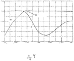
- Figure 4 shows the frequency response of the high pass filter HPF.
- the diagram shows the currents Is, Io and Ir in dependence of frequency.
- the axes of the diagram are logarithmic.
- a sensed current Is of 10mA is applied and the responding output current lo and resulting current Ir are measured.
- the sensed current Is is a constant line in the diagram.
- the corner frequency of the high-pass filter HPF is chosen to be 800Hz resulting in a ratio of Ir/Is equal to 0.01 at 8kHz giving a corresponding attenuation of 40dB.
- the corner frequency can be selected at other frequencies and is typically selected to give 40dB at the fundamental of the switching frequency, which may be typically equal or larger than 4kHz.
- the shape of the resulting current Ir should be mentioned. Of particular importance is the low frequency rejection in the stop band, the corner frequency without ringing (critically damped) and the sharp roll-off above corner frequency, which is about 40dB/dec. Furthermore, a good attenuation, which is larger than 40dB, extends well above 150kHz, thus providing attenuation enhancement in the EMC band as well as at the switching fundamental.
- FIG. 5 shows an exemplary circuit diagram in detail of the high-pass filter HPF having a filter input HPFIN for being coupled to the sensor terminal CTN.
- the output HPFOUT may be coupled to the output terminal OUT.
- the high-pass filter HPF is coupled to the amplifier means 12 and has an input 27, which may be the non-inverting input 15, and an output 28, which may be the buffer outputs 19, 21.
- the input HPFIN is connected with the input 27 of the amplifier means 12 via a resistor R6 and a capacitor C4 that are connected in parallel.
- the output 28 of the amplifier means 12 is connected with the input 27 via a series connection of a resistor R5 and a capacitor C3 coupled in parallel, a capacitor C2 and a resistor R4.
- a resistor R3 is connected with the resistor R4 and a reference potential.
- the high-pass filter HPF filters the sensor current.
- the high-pass filter HPF includes a bootstrap connection, where the amplifier output 28 is fed back to its input 27 via the dc blocking capacitor C2 and a suitable RC network which is formed by the resistor R5 and the capacitor C3.
- FIG. 6 shows an embodiment of the filter device 4 in more detail.
- the filter device 4 includes the sensor terminals CTN, CTP, the output terminal OUT, the power supply means terminals AC1, AC2 and the terminal for applying a reference potential GND.
- the filter device 4 also comprises a high-pass filter HPF including the components R6, C4, R4, R3, C2, R5, and C3 being coupled as described in connection with Figure 4 .
- the filter device 4 comprises an operational amplifier U1 being coupled with the buffer amplifiers U2, U3 forming the amplifier means 12 as described in connection with Figure 3 .
- the power supply unit PSU supplies the amplifiers U1, U2, U3.
- the filter device 4 also includes diodes D1, D2, D3, D4 for protecting the amplifier from line disturbance.
- FIG. 7 shows a circuit arrangement including the filter device 4 being part of a three-phase ac line filter.
- the filter device 4 is embodied as a module, which is connected with the other components of the circuit arrangement.
- This circuit arrangement forms a three-phase hybrid filter with a common mode attenuation boost.
- the circuit arrangement is coupled between the lines L1, L2, L3 of a power supply network and the electrically operated appliance L1', L2', L3' or load. Furthermore, there is a reference line PE / PE' connected with the reference potential.
- the appliance may produce undesired noise, switching pulses, spikes, and high frequency noise. These effects should be filtered out in order to comply with electromagnetic compatibility specifications.
- the sensing device is a current transformer CT and the necessary active filter device electronics are all integrated into a self-contained component block forming the filter device module.
- the filter device 4 includes the high pass filter HPF, the amplifier means 12 and the auxiliary power supply unit PSU as described in connected with the previous figures.
- the blocking capacitor Co connected downstream to the output OUT of the filter device 4 provides power line voltage isolation.
- the combination of two capacitors Cps form a voltage divider to produce a suitable input voltage for the power supply unit PSU.
- the remaining components may be those typically found in a passive line filter.
- the passive filter section includes a low-pass filter formed by inductive components L2. Furthermore, there an arrangement of capacitors Cx1 and an arrangement of capacitors Cx2 and resistors Rx2 connected in parallel. The neutral point of the arrangement of the capacitors Cx2 and the resistors Rx2 is connected with the reference potential by a parallel connection of a resistor Ry2 and a capacitor Cy2. Other arrangements are possible.
- Figure 8 indicates an application of the filter device 4 which allows determination of suitable values for the components connected to the filter device 4.
- FIG 8 shows a simplified circuit diagram of a typical system integration of the filter device 4.
- the sensed current Is and the compensation current Io are added at the summing point 24 in order to reduce the disturbances.
- the compensation current Io flows via a coupling capacitor Co.
- the circuit further comprises a voltage source Vn for generating a signal, which is characterised by the voltage V and the frequency Fsw, and a capacitor Cn downstream to the voltage source Vn.
- the circuit further comprises a line-to-ground capacitor Cy coupled in parallel with the voltage source Vn and the capacitor Cn. Furthermore, there is an in-line inductive impedance Lc.
- Suitable values of the components Cy, Lc and Co, to cope with the disturbing noise current In depend on the values of Cn, V and Fsw characterising the disturbance. Furthermore, the values of the predicted compensation current Io and voltage Vo provided at the output of the filter device 4 must fall within specified limits of the filter device 4.
- the resulting current Ir is predicted in such a manner that it falls into an EMI disturbance level which should comply with the necessary EMC and earth leakage current requirements.
- the adaption and selection of the components Lc, Co and Cy for a system to be designed may be made from a graph or table which is based on simulation, with varying parameters Fsw, Vn, Cn, or can be made by calculation from a formula. Such adaption and selection result in optimal working conditions and ensure correct operation.
Description
- The present invention is directed to an active filter device. The invention is further directed to a filtering circuit arrangement including the active filter device. The filtering circuit arrangement may serve as a power line filter, which may be connected between a power supply network and an electrically operated appliance.
- Filters may be used on power lines for the mitigation of electromagnetic noise, or earth leakage current, which may be generated by switching frequencies, for example.
- For instance, on motor drive output lines, earth leakage current can result in a rapid degradation of motor bearings. In many applications, a system switching frequency exists in the range of 1KHz to 150kHz. In the case of motor drives, switching frequencies are typically in the range of 1kHz to 16kHz and in the case of power supplies, UPS and power conversion they are typically in the range of 10kHz to 200kHz.
- It is desirable to find efficient ways to remove these disturbing frequencies, and associated harmonics, from both input and output lines.
- Conventional filter solutions for mitigating electromagnetic noise on power lines, which are generated for example by the switching frequencies, are passive filters constructed with inductive and capacitive elements and resistors.
- Power electronic equipment may employ line filtering that is constructed with such inductive and capacitive elements in order to attenuate line disturbances. The impedance of these passive elements is frequency dependent. In order to achieve the desired attenuation, the passive elements are often large and expensive, especially at low frequencies.
- More compact filter solutions are desired, in particular in the frequency range of 1kHz to 150kHz where, in addition to switching frequencies, further phenomena in the field of electromagnetic compatibility (EMC) exist such as: spurious tripping of residual current devices (RCDs), disturbance to power line communications, and more generally earth leakage current.
- Suitable filters for this purpose may either be built to be ever larger and more expensive; or where this becomes too extreme, the problem is ignored altogether.
-
WO 2014/048471 A1 describes an EMC filtering device comprising an active filtering section and a passive bandwidth filtering section. The passive and active parts of the filter are mutually beneficial such that the resultant filter has a hybrid nature, is small, and has a lower cost than a passive filter solution alone. - Active filter devices are also shown in Wang, P. et al.: "Research and Design of a Common Mode Hybrid EMI Filter for Switch-mode Power Supply", Wang, S. et al.: "Investigation of Hybrid EMI Filters for Common-Mode EMI Suppression in a Motor Drive System",
GB 2326995 A WO 2008/020029 A1 . - It is an aim of the invention to provide an alternative, compact filter device.
- This aim is achieved by an active filter device according to claim 1, the active filter device comprising:
- sensor terminals for applying a sensor signal depending on a sensed noise signal,
- an output terminal for providing a correction signal that is suitable for reducing the noise signal,
- a signal source being adapted for generating the correction signal and comprising a unity gain amplifier means,
- a high-pass filter being coupled between the sensor terminals and the signal source,
- The unity gain amplifier means comprises an operational amplifier having a non-inverting input, an inverting input and an output, the latter being coupled to the inverting input, and the high-pass filter being coupled to the non-inverting input. The high pass filter comprises a bootstrap connection, where an output of the unity gain amplifier means is coupled to an input of the unity gain amplifier means and the bootstrap connection comprises a dc blocking capacitor being coupled in series with a resistor and a capacitor that are coupled in parallel.
- An active filter is a type of analog electronic filter that includes active components such as an amplifier. The use of active components allows for a compact design of the filter device, on the one hand. One the other hand, a power supply for the active components is required.
- The sensor terminals may be terminals for coupling a separate sensor component to the filter device. Alternatively, the sensor terminals are parts of a sensor that is an integral part of the filter device.
- Coupling two components means that the components are electrically connected by a conductive joint, e.g. a conductor line, or by at least one further component that is coupled between the components, e.g. a resistor or a resistor-and-capacitor-network. Connecting two components means that the components are directly electrically connected by a conductive joint.
- The signal source may comprise an amplifier for proving the correction signal. The filter device recognises the importance of a high gain bandwidth for the amplifier and allows a correct frequency response of the amplifier. The use of a high-pass filter at the input of the signal source including the amplifier allows the production of a frequency response, which, in particular, has a very flat stop band, a corner frequency without ringing and a rapid transition to the pass band. The signal is damped in order to avoid undesirable ringing of the signal in the time domain by means of appropriated formed filter frequency response. Without a high pass filter at the amplifier input, the voltage or current dynamic range of the amplifier is too easily saturated.
- In one embodiment, the noise signal, the correction signal and the signal source are a noise current, a correction current and a current source, respectively. In other words, the filter device operates on the principle of current compensation. Alternatively, the noise signal, the correction signal and the signal source are a noise voltage, a correction voltage and a voltage source, respectively. In other words, the filter device operates on the principle of voltage compensation.
- The active filter device forms a feed-forward control where the correction signal depends on the sensed noise signal. Such a control system that has only feed-forward behaviour responds to its controlling high-pass filtered sensor signal in a predefined way without responding to how the output reacts. The signal source acts in such a manner that the correction signal compensates or nearly compensates the noise signal. In other words, their sum is equal or nearly equal to zero.
- The signal source comprises a unity gain amplifier means, which essentially provides the input voltage at the output. The unity gain amplifier means may comprise an operational amplifier with a closed loop feedback. In one embodiment, the operational amplifier has a non-inverting input, an inverting input and an output, the latter being coupled to the inverting input. An output of the high-pass filter is coupled to the non-inverting input. In one embodiment, a buffer amplifier or a multitude of buffer amplifiers that are coupled in parallel are coupled between the output and the inverting input of the operational amplifier.
- The use of amplifiers with a very large bandwidth and open loop gain-bandwidth product results in a very linear and clean, EMC-wise, residual signal.
- The high pass filter comprises a bootstrap connection where a part of the output signal of an amplifier stage is applied to the input. The bootstrap connection comprises a dc blocking capacitor being coupled in series with a resistor and a capacitor that are coupled in parallel. Other components in the bootstrap connection are possible.
- The filter device may include a power supply unit coupled to the unity gain amplifier means, and power supply means terminals for applying a voltage to the power supply unit. The power supply unit allows supply of power to the active components of the filter device.
- The integration of all aforementioned components into one compact and self-contained block may form a filter device module. Signal cancellation can be achieved with this block module together with a sensing device that is coupled with the module. In one embodiment, such a block module may provide current cancellation when connected to a suitable current transformer.
- Alternatively, a module may be built in such a manner that it includes further components, e.g. the sensing device and/or further passive filter components. Although such a filter which includes passive filter elements it is still considered as an active filter device.
- The active filter device may be comprised of a circuit arrangement connectable between a power supply network and an electrically operated appliance. The circuit arrangement may further comprise a current sensor being coupled to the signal sensor terminals and comprising a current transformer. The sensor may be a component coupled with the filter device module. Alternatively, the circuit arrangement may comprise a voltage sensor.
- In one embodiment, the output terminal of the active filter device is coupled with a summing point between the current transformer and the connection to the power network or the electrically operated appliance. Providing the correction current at the summing point allows reduction of the sensed noise current, which causes compensation of the disturbances.
- The power network may include one of: a dc power line; an ac power line; a single phase power line; and a multiple phase power line. Additionally, the power network may include one of: a power supply line; and a power output line, such as a motor feed cable.
- There is a broad field of application for the above-mentioned filter device and the circuit arrangement. Potential use may be in the industrial, domestic, medical and automotive fields. It may be used for both input and output filtering. It may be used on single wire and double wire, low and high voltage dc supplies, single phase, three phase and three phase neutral, low and medium voltage ac supplies. In the field of automotive voltage dc supplies it may be used where the circuit arrangement is connected to an EMC filtering device connected to an electric driven motor.
- Features which are described herein above and below in conjunction with different aspects or embodiments, may also apply to other aspects and embodiments. Further features and advantageous embodiments of the subject-matter of the disclosure will become apparent from the following description of the exemplary embodiments in conjunction with the figures, in which:
-
Figure 1 shows a circuit diagram of an exemplary embodiment of a power line with voltage cancellation. -
Figure 2 shows a circuit diagram of an exemplary embodiment of a power line with current cancellation. -
Figure 3 shows a simplified circuit diagram of current cancellation on apower line 3. -
Figure 4 shows the frequency response of an embodiment of a high-pass filter. -
Figure 5 shows a circuit diagram of an embodiment of a high-pass filter -
Figure 6 shows an embodiment of the filter device in more detail. -
Figure 7 shows a circuit diagram of an embodiment of an arrangement including the filter device being part of a three-phase ac line filter. -
Figure 8 shows a circuit diagram indicating the application of the filter device. -
Figures 1 and 2 illustrate the method of filtering operation, which works in principle as follows. The disturbance on a power line, which is a noise signal, is detected by a sensing device which passes a sensor signal, via a high pass filter, to an amplifying device serving as the signal source. It produces an output signal serving as a correction signal which, over a designated bandwidth, has very nearly the same phase and magnitude as that detected by the sensing device. This can be described as a unity-gain feed-forward control path, wherein the gain is unity. Feed-forward is a term describing passing a controlling signal from a source to a load. A control system that has only feed-forward behaviour responds to its control signal in a pre-defined way without responding to how the load reacts. - The inverse of the output signal is summed with the sensed signal at, or over, a suitable summing point, or component, on the power line. The resulting signal on the power line, after summing, is reduced very nearly to zero.
- The disturbance cancellation can be realised as voltage or current type as shown in
Figures 1 and 2 , respectively. -
Figure 1 shows a circuit diagram of a power line with voltage cancellation. The circuit comprises a voltage source Vn which provides a voltage supply for a voltage compensation means 1 connected in parallel with an inductive impedance Lo and an load impedance Z, connected in series with the aforementioned voltage compensation means 1 and the inductive impedance Lo. The voltage compensation means 1 is adapted for sensing a noise voltage Vs on the voltage supply side and then providing a voltage Vo in dependence on the sensed noise voltage Vs. The voltage cancellation is achieved over the inductive impedance Lo to ensure power line current continuity. - The resulting voltage Vr is the sum of the sensed noise voltage Vs and the compensation voltage Vo, which should be as close as possible to zero. In other words, Vr = Vs-Vo ≈ 0 when Vs ≈ Vs where Vs, Vo and Vr are all voltage vectors.
-
Figure 2 shows a circuit diagram of a power line with current cancellation. The circuit comprises a current source In which provides current supply for a current compensation means 2 connected in series with a capacitive impedance Co and an load impedance Z that is connected in parallel with the aforementioned current compensation means 2 and the capacitive impedance Co. The current compensation means 2 is adapted for detecting a noise current Is of the current source In by means of a sensor 5 and then providing a compensation current Io in dependence of the detected noise current Is. The current cancellation is achieved via the capacitive impedance Co to ensure power line voltage isolation. - The resulting current Ir is the sum of the sensed current Is and the compensation current Io, which should be as close as possible to zero. In other words, Ir = Is-Io ≈ 0 when Is ≈ Is where Is, Io and Ir are all current vectors.
-
Figure 3 shows an embodiment of a simplified circuit diagram of current cancellation of apower line 3. The current cancellation is performed by anactive filter device 4 which may be embodied as a module and further components that are coupled between thepower line 3 and thefilter device 4. - The current cancellation circuit comprises a current sensor 5 including a current transformer CT. Typically it has secondary turns N = 100. The current transformer CT comprises terminals 7, 8 that are connected to the
filter device 4. - The
filter device 4 has sensor terminals CTN, CTP for applying a sensor signal depending on a noise current Is on thepower line 3; the sensor 5 providing the sensor signal. Furthermore, there is an output terminal OUT and a terminal for applying a reference potential GND. Power supply means terminals AC1, AC2 allow applying power supply for the active components to thefilter device 4. - The current cancellation circuit comprises a high-pass filter HPF, an amplifier means 12 and a power supply unit PSU.
- The high-pass filter HPF is coupled between one sensor terminal CTN and amplifier means 12.
- The amplifier means 12 being a unity gain amplifier means comprises an operational amplifier U1, and two buffer amplifiers U2, U3. The operational amplifier U1 has a
non-inverting input 15, an inverting input 14, and an output 16. Each buffer amplifier U2, U3 has aninput output inputs outputs non-inverting input 15 is coupled to the high-pass filter HPF. - The
outputs filter device 4. - A power supply unit PSU is coupled to the power supply means terminals AC1, AC2 and the amplifier means 12. The power supply means terminals AC1, AC2 and the amplifier means 12 are also connected with the terminal for applying a reference potential GND. Alternatively the power supply PSU may be removed from the
filter device 4, whereby dc power for the amplifier means 12 is provided from a separate or external auxiliary power source. - A resistor serving as burden resistor Rb is coupled between the sensor terminals CTN, CTP. One sensor terminal CTP is connected to the output OUT.
- The output terminal OUT is coupled via a coupling capacitance Co to the
power line 3. The connection of thepower line 3 and the capacitance's terminal serves as summingpoint 24 at which the noise current Is and the correction current Io provided by thefilter device 4 are summed. Capacitor Co provides safety isolation of the power line to earth. - The terminals 7, 8 of the current transformer CT are connected with the sensor terminals CTN, CTP of the
filter device 4, where the current transformer CT is terminated in the burden resistor Rb which may have a typical resistance of 220R. - The voltage across the burden resistor Rb passes via the high-pass filter HPF and the unity gain amplifier means 12, which comprises the operational amplifier U1 and the buffer amplifiers U2, U3.
- In the pass band, the voltage across the output resistor Ro, which may have a typical value of 2.2R, and the burden resistor Rb is equal.
- The correction current Io is given in terms of the sensed current Is by the expression Io = Is Rb / (N Ro), wherein the values for Rb, N and Ro are chosen to achieve equal noise and compensation currents, i.e. Io ≈ Is. Typical values of the components have been given above.
- The amplifier means 12 is a high quality, wide band, unity gain amplifier means, formed from the operational amplifier U1 with a very high gain-bandwidth product, typically 200MHz, and the buffer amplifiers U2 and U3 with bandwidths of about 180MHz. The buffer amplifiers U2 and U3 are connected in parallel to increase the drive current.
- The
outputs outputs non-inverting input 15 of the operational amplifier U1. - The high gain of the operational amplifier U1 and the wide bandwidth of all components ensure that not only wide band current cancellation, but also a high quality, linear and noise free resulting current Ir is achieved. The wide bandwidth enables satisfactory results to be achieved.
-
Figure 4 shows the frequency response of the high pass filter HPF. The diagram shows the currents Is, Io and Ir in dependence of frequency. The axes of the diagram are logarithmic. - A sensed current Is of 10mA is applied and the responding output current lo and resulting current Ir are measured. The sensed current Is is a constant line in the diagram.
- In this configuration, the corner frequency of the high-pass filter HPF is chosen to be 800Hz resulting in a ratio of Ir/Is equal to 0.01 at 8kHz giving a corresponding attenuation of 40dB. The corner frequency can be selected at other frequencies and is typically selected to give 40dB at the fundamental of the switching frequency, which may be typically equal or larger than 4kHz.
- The shape of the resulting current Ir should be mentioned. Of particular importance is the low frequency rejection in the stop band, the corner frequency without ringing (critically damped) and the sharp roll-off above corner frequency, which is about 40dB/dec. Furthermore, a good attenuation, which is larger than 40dB, extends well above 150kHz, thus providing attenuation enhancement in the EMC band as well as at the switching fundamental.
-
Figure 5 shows an exemplary circuit diagram in detail of the high-pass filter HPF having a filter input HPFIN for being coupled to the sensor terminal CTN. The output HPFOUT may be coupled to the output terminal OUT. The high-pass filter HPF is coupled to the amplifier means 12 and has aninput 27, which may be thenon-inverting input 15, and anoutput 28, which may be the buffer outputs 19, 21. The input HPFIN is connected with theinput 27 of the amplifier means 12 via a resistor R6 and a capacitor C4 that are connected in parallel. Theoutput 28 of the amplifier means 12 is connected with theinput 27 via a series connection of a resistor R5 and a capacitor C3 coupled in parallel, a capacitor C2 and a resistor R4. A resistor R3 is connected with the resistor R4 and a reference potential. - The high-pass filter HPF filters the sensor current. In order to achieve a suitable shape for the residual current Ir the high-pass filter HPF includes a bootstrap connection, where the
amplifier output 28 is fed back to itsinput 27 via the dc blocking capacitor C2 and a suitable RC network which is formed by the resistor R5 and the capacitor C3. Exemplary values of the components may be R3 = 220kΩ, R4 = 220kΩ, R5 = 15 kΩ, R6 = 56kΩ, C2 = 3.3 µF, C3 = 1nF, and C4 = 2.2nF. -
Figure 6 shows an embodiment of thefilter device 4 in more detail. Thefilter device 4 includes the sensor terminals CTN, CTP, the output terminal OUT, the power supply means terminals AC1, AC2 and the terminal for applying a reference potential GND. - The
filter device 4 also comprises a high-pass filter HPF including the components R6, C4, R4, R3, C2, R5, and C3 being coupled as described in connection withFigure 4 . - Furthermore, the
filter device 4 comprises an operational amplifier U1 being coupled with the buffer amplifiers U2, U3 forming the amplifier means 12 as described in connection withFigure 3 . The power supply unit PSU supplies the amplifiers U1, U2, U3. Thefilter device 4 also includes diodes D1, D2, D3, D4 for protecting the amplifier from line disturbance. - Further inductive, capacitive and resistive impedances allow improved filtering and stabilise the operation of the components according to the basic principles as described in connection with the previous figures.
-
Figure 7 shows a circuit arrangement including thefilter device 4 being part of a three-phase ac line filter. In this embodiment, thefilter device 4 is embodied as a module, which is connected with the other components of the circuit arrangement. This circuit arrangement forms a three-phase hybrid filter with a common mode attenuation boost. - The circuit arrangement is coupled between the lines L1, L2, L3 of a power supply network and the electrically operated appliance L1', L2', L3' or load. Furthermore, there is a reference line PE / PE' connected with the reference potential.
- The appliance may produce undesired noise, switching pulses, spikes, and high frequency noise. These effects should be filtered out in order to comply with electromagnetic compatibility specifications.
- The sensing device is a current transformer CT and the necessary active filter device electronics are all integrated into a self-contained component block forming the filter device module. The
filter device 4 includes the high pass filter HPF, the amplifier means 12 and the auxiliary power supply unit PSU as described in connected with the previous figures. - The blocking capacitor Co connected downstream to the output OUT of the
filter device 4 provides power line voltage isolation. The combination of two capacitors Cps form a voltage divider to produce a suitable input voltage for the power supply unit PSU. - The remaining components may be those typically found in a passive line filter. The passive filter section includes a low-pass filter formed by inductive components L2. Furthermore, there an arrangement of capacitors Cx1 and an arrangement of capacitors Cx2 and resistors Rx2 connected in parallel. The neutral point of the arrangement of the capacitors Cx2 and the resistors Rx2 is connected with the reference potential by a parallel connection of a resistor Ry2 and a capacitor Cy2. Other arrangements are possible. The inductance L1 is typically a ferrite core with straight-through coupling (N=1) which provides improved immunity from line disturbances.
-
Figure 8 indicates an application of thefilter device 4 which allows determination of suitable values for the components connected to thefilter device 4. -
Figure 8 shows a simplified circuit diagram of a typical system integration of thefilter device 4. The sensed current Is and the compensation current Io are added at the summingpoint 24 in order to reduce the disturbances. The compensation current Io flows via a coupling capacitor Co. The circuit further comprises a voltage source Vn for generating a signal, which is characterised by the voltage V and the frequency Fsw, and a capacitor Cn downstream to the voltage source Vn. The circuit further comprises a line-to-ground capacitor Cy coupled in parallel with the voltage source Vn and the capacitor Cn. Furthermore, there is an in-line inductive impedance Lc. - Suitable values of the components Cy, Lc and Co, to cope with the disturbing noise current In, depend on the values of Cn, V and Fsw characterising the disturbance. Furthermore, the values of the predicted compensation current Io and voltage Vo provided at the output of the
filter device 4 must fall within specified limits of thefilter device 4. - The resulting current Ir is predicted in such a manner that it falls into an EMI disturbance level which should comply with the necessary EMC and earth leakage current requirements.
- The adaption and selection of the components Lc, Co and Cy for a system to be designed may be made from a graph or table which is based on simulation, with varying parameters Fsw, Vn, Cn, or can be made by calculation from a formula. Such adaption and selection result in optimal working conditions and ensure correct operation.
- The scope of protection is not limited to the examples given herein above.
-
- 1
- voltage compensation means
- 2
- current compensation means
- 3
- power line
- 4
- filter device
- 5
- sensor
- 7, 8, HPFIN, HPFOUT
- terminals
- 12
- amplifier means
- 14, 15, 18, 20, 27
- input
- 16, 19, 21, 28
- output
- 24
- summing point
- U1, U2, U3
- amplifiers
- Io, Is, Ir
- current
- Vo, Vs, Vr, V
- voltage
- Fsw
- frequency
- CTN, CTP, OUT, AC1, AC2, GND
- terminals of the filter device
- HPF
- high-pass filter
- PSU
- power supply unit
- CT
- current transformer
- Rb, Ro, Ry2, Rx2, R3, R4, R5, R6
- resistors
- Cx1, Cx2, Cy2, Cps, Co, C2, C3, C4
- capacitors
- L1, L2, Lo
- inductive impedance
- Z
- load impedance
- L1, L2, L3, PE, L1', L2', L3', PE'
- lines
- In
- current source
- Vn
- voltage source
Claims (9)
- An active filter device (4) comprising:- sensor terminals (CTN, CTP) for applying a sensor signal depending on a sensed noise signal (Is, Vs),- an output terminal (OUT) for providing a correction signal (Io, Vo) that is suitable for reducing the noise signal (Is, Vs),- a signal source (1, 2, 12) being adapted for generating the correction signal (Io, Vo) and comprising a unity gain amplifier means (12),- a high-pass filter (HPF) being coupled between the sensor terminals (CTN, CTP) and the signal source,wherein the correction signal (Io, Vo) is generated with dependence on the high-pass filtered sensor signal characterised in that
the unity gain amplifier means (12) comprises an operational amplifier (U1) having a non-inverting input (15), an inverting input (14) and an output (16), the latter being coupled to the inverting input (14), and the high-pass filter (HPF) being coupled to the non-inverting input (15),
the high pass filter (HPF) comprises a bootstrap connection, where an output of the unity gain amplifier means (12) is coupled to an input of the unity gain amplifier means (12) and the bootstrap connection comprises a DC blocking capacitor (C2) being coupled in series with a resistor (R5) and a capacitor (C3) that are coupled in parallel. - The active filter device (4) of claim 1, wherein
the noise signal, the correction signal and the signal source are a noise current (Is), a correction current (Io) and a current source (2, 12), respectively. - The active filter device (4) of claim 1, wherein
the noise signal, the correction signal and the signal source are a noise voltage (Vs), a correction voltage (Vo) and a voltage source (2), respectively. - The active filter device (4) of any of the previous claims,
being a feed-forward control, the signal source (1, 2, 12) being controlled in such a manner that the correction signal (Io, Vo) compensates the noise signal (Is, Vs). - The active filter device (4) of any of the previous claims, further comprising a buffer amplifier or a multitude of buffer amplifiers (U2, U3) that are coupled in parallel, coupled between the output (16) and the inverting input (14) of the operational amplifier (U1).
- The active filter device (4) of any of the previous claims, comprising- a power supply unit (PSU) coupled to the unity gain amplifier means (12), and- power supply means terminals (AC1, AC2) for applying a voltage to the power supply unit (PSU).
- A circuit arrangement connectable between a power supply network and an electrically operated appliance, comprising- the active filter device (4) of one of the claims 2 and 4 to 6, and- a current sensor (5) being coupled to the signal sensor terminals (CTN, CTP) and comprising a current transformer (CT).
- The circuit arrangement of claim 7, wherein
the output terminal (OUT) is coupled with a summing point (24) between the current transformer (CT) and the connection to the power network or to the electrically operated appliance. - The circuit arrangement of claim 7 or 8, wherein
the power network is one of a a DC power line, an AC power line, a single phase power line, and a multiple phase power line.
Priority Applications (5)
| Application Number | Priority Date | Filing Date | Title |
|---|---|---|---|
| EP14167918.3A EP2945268B1 (en) | 2014-05-12 | 2014-05-12 | Active filter device and circuit arrangement comprising an active filter device |
| CN201580024726.1A CN106464125B (en) | 2014-05-12 | 2015-04-28 | Active filter device and circuit arrangement including active filter device |
| PCT/EP2015/059182 WO2015173006A1 (en) | 2014-05-12 | 2015-04-28 | Active filter device and circuit arrangement comprising an active filter device |
| US15/310,011 US10069480B2 (en) | 2014-05-12 | 2015-04-28 | Active filter device and circuit arrangement comprising an active filter device |
| JP2016567630A JP6513706B2 (en) | 2014-05-12 | 2015-04-28 | Circuit assembly comprising an active filter device and an active filter device |
Applications Claiming Priority (1)
| Application Number | Priority Date | Filing Date | Title |
|---|---|---|---|
| EP14167918.3A EP2945268B1 (en) | 2014-05-12 | 2014-05-12 | Active filter device and circuit arrangement comprising an active filter device |
Publications (2)
| Publication Number | Publication Date |
|---|---|
| EP2945268A1 EP2945268A1 (en) | 2015-11-18 |
| EP2945268B1 true EP2945268B1 (en) | 2019-12-18 |
Family
ID=50693513
Family Applications (1)
| Application Number | Title | Priority Date | Filing Date |
|---|---|---|---|
| EP14167918.3A Active EP2945268B1 (en) | 2014-05-12 | 2014-05-12 | Active filter device and circuit arrangement comprising an active filter device |
Country Status (5)
| Country | Link |
|---|---|
| US (1) | US10069480B2 (en) |
| EP (1) | EP2945268B1 (en) |
| JP (1) | JP6513706B2 (en) |
| CN (1) | CN106464125B (en) |
| WO (1) | WO2015173006A1 (en) |
Families Citing this family (12)
| Publication number | Priority date | Publication date | Assignee | Title |
|---|---|---|---|---|
| US10700625B2 (en) | 2016-12-12 | 2020-06-30 | Mitsubishi Electric Corporation | Power conversion device |
| DE102017104894B4 (en) | 2017-03-08 | 2022-01-20 | Tdk Electronics Ag | Active compensation circuit and system |
| US10374510B2 (en) * | 2017-04-07 | 2019-08-06 | Texas Instruments Incorporated | Compensated active electro-magnetic interference filters |
| DE102018102122A1 (en) | 2018-01-31 | 2019-08-01 | Tdk Electronics Ag | Machines with power electronic energy converters and leakage current compensation and system |
| DE102018103438A1 (en) * | 2018-02-15 | 2019-08-22 | Tdk Electronics Ag | Compensation filter and method for commissioning a compensation filter |
| DE102018103391A1 (en) * | 2018-02-15 | 2019-08-22 | Tdk Electronics Ag | Compensation filter and method for commissioning a compensation filter |
| EP3664305B1 (en) * | 2018-12-03 | 2023-02-08 | Schaffner EMV AG | Electronic decoupling impedance |
| DE102019129413B4 (en) | 2019-10-31 | 2021-10-07 | Dr. Ing. H.C. F. Porsche Aktiengesellschaft | Compensation device for leakage currents |
| CN113348614B (en) * | 2020-11-06 | 2023-08-15 | 香港应用科技研究院有限公司 | Active filter for reducing electromagnetic interference using single junction and negative impedance converter |
| US11303264B1 (en) | 2020-11-06 | 2022-04-12 | Hong Kong Applied Science and Technology Research Institute Company Limited | Active filter for electromagnetic interference (EMI) reduction using a single connection point and a negative impedance converter |
| US20220416652A1 (en) * | 2021-06-28 | 2022-12-29 | Richtek Technology Corporation | Switching power converter and active emi filter circuit thereof |
| CN114935970B (en) * | 2022-04-29 | 2023-07-14 | 苏州浪潮智能科技有限公司 | Current sharing method, device and system for server power supply module |
Family Cites Families (8)
| Publication number | Priority date | Publication date | Assignee | Title |
|---|---|---|---|---|
| US5300896A (en) * | 1992-10-16 | 1994-04-05 | Suesserman Michael F | Bootstrapped, AC-coupled differential amplifier |
| GB9713878D0 (en) * | 1997-06-30 | 1997-09-03 | Roxburgh Electronics Ltd | Mains filtering circuit |
| JP2001119258A (en) * | 1999-10-19 | 2001-04-27 | Hitachi Metals Ltd | Branching filter |
| US7154254B2 (en) | 2004-06-18 | 2006-12-26 | Agilent Technologies, Inc. | Apparatus and method for improving electromagnetic compatibility |
| WO2008020029A1 (en) * | 2006-08-15 | 2008-02-21 | Schaffner Emv Ag | Low-leakage emc filter |
| WO2013111360A1 (en) * | 2012-01-27 | 2013-08-01 | 三菱電機株式会社 | High-frequency current reduction device |
| WO2014048471A1 (en) | 2012-09-26 | 2014-04-03 | Schaffner Emv Ag | Power line filter device |
| US8823448B1 (en) * | 2013-03-29 | 2014-09-02 | Hamilton Sundstrand Corporation | Feed forward active EMI filters |
-
2014
- 2014-05-12 EP EP14167918.3A patent/EP2945268B1/en active Active
-
2015
- 2015-04-28 CN CN201580024726.1A patent/CN106464125B/en active Active
- 2015-04-28 US US15/310,011 patent/US10069480B2/en active Active
- 2015-04-28 JP JP2016567630A patent/JP6513706B2/en active Active
- 2015-04-28 WO PCT/EP2015/059182 patent/WO2015173006A1/en active Application Filing
Non-Patent Citations (1)
| Title |
|---|
| None * |
Also Published As
| Publication number | Publication date |
|---|---|
| EP2945268A1 (en) | 2015-11-18 |
| WO2015173006A1 (en) | 2015-11-19 |
| JP6513706B2 (en) | 2019-05-15 |
| US20170179931A1 (en) | 2017-06-22 |
| JP2017516446A (en) | 2017-06-15 |
| CN106464125B (en) | 2019-10-18 |
| US10069480B2 (en) | 2018-09-04 |
| CN106464125A (en) | 2017-02-22 |
Similar Documents
| Publication | Publication Date | Title |
|---|---|---|
| EP2945268B1 (en) | Active filter device and circuit arrangement comprising an active filter device | |
| EP2787618B1 (en) | Voltage fed feed forward active EMI filter | |
| US8823448B1 (en) | Feed forward active EMI filters | |
| TWI399017B (en) | Active emc filter for machine tools | |
| US9722484B2 (en) | Noise filtering | |
| WO2014048471A1 (en) | Power line filter device | |
| JP5560024B2 (en) | Harmonic filter | |
| EP3651385B1 (en) | Control circuit for suppressing electromagnetic interference signals | |
| US20230179090A1 (en) | Active electromagnetic interference filter with damping network | |
| US20210313966A1 (en) | Active electromagnetic interference (emi) filter for common-mode emi reduction | |
| US9577707B1 (en) | Method and device for stabilizing impedance on a power-line communication device | |
| Yang et al. | Implementation of a MOSFET-based active differential mode EMI filter in DC/DC converter | |
| KR20170019404A (en) | Power compensating apparatus including active dc-link circuit and method for compensating power using active dc-link circuit | |
| JP2008530836A (en) | Active EMC filters for medical applications | |
| EP0995266B1 (en) | Mains filter circuit arrangement | |
| CN106899018B (en) | Active filtering system | |
| US5737198A (en) | Hybrid active power filter with programmed impedance characteristics | |
| US11664777B2 (en) | DC filter device | |
| KR101039310B1 (en) | Hybrid Active Power Filter | |
| Goswami et al. | Modeling and analysis of hybrid differential mode filters for AC/DC converters to suppress current ripples and EMI | |
| WO2015177746A1 (en) | Active emi differential mode line filter | |
| EP4300822A1 (en) | Active emi filter | |
| US20230163681A1 (en) | Electromagnetic interference suppression circuit | |
| RU2342758C1 (en) | Method of reducing capacitive enclosure leakage currents on power-line filters of radio interference | |
| CN115441454A (en) | Harmonic suppression device and method |
Legal Events
| Date | Code | Title | Description |
|---|---|---|---|
| PUAI | Public reference made under article 153(3) epc to a published international application that has entered the european phase |
Free format text: ORIGINAL CODE: 0009012 |
|
| 17P | Request for examination filed |
Effective date: 20140512 |
|
| AK | Designated contracting states |
Kind code of ref document: A1 Designated state(s): AL AT BE BG CH CY CZ DE DK EE ES FI FR GB GR HR HU IE IS IT LI LT LU LV MC MK MT NL NO PL PT RO RS SE SI SK SM TR |
|
| AX | Request for extension of the european patent |
Extension state: BA ME |
|
| RAP1 | Party data changed (applicant data changed or rights of an application transferred) |
Owner name: EPCOS AG |
|
| RAP1 | Party data changed (applicant data changed or rights of an application transferred) |
Owner name: TDK ELECTRONICS AG |
|
| GRAP | Despatch of communication of intention to grant a patent |
Free format text: ORIGINAL CODE: EPIDOSNIGR1 |
|
| STAA | Information on the status of an ep patent application or granted ep patent |
Free format text: STATUS: GRANT OF PATENT IS INTENDED |
|
| INTG | Intention to grant announced |
Effective date: 20190802 |
|
| GRAS | Grant fee paid |
Free format text: ORIGINAL CODE: EPIDOSNIGR3 |
|
| GRAA | (expected) grant |
Free format text: ORIGINAL CODE: 0009210 |
|
| STAA | Information on the status of an ep patent application or granted ep patent |
Free format text: STATUS: THE PATENT HAS BEEN GRANTED |
|
| RIN1 | Information on inventor provided before grant (corrected) |
Inventor name: TUCKER, ANDREW |
|
| AK | Designated contracting states |
Kind code of ref document: B1 Designated state(s): AL AT BE BG CH CY CZ DE DK EE ES FI FR GB GR HR HU IE IS IT LI LT LU LV MC MK MT NL NO PL PT RO RS SE SI SK SM TR |
|
| REG | Reference to a national code |
Ref country code: CH Ref legal event code: EP |
|
| REG | Reference to a national code |
Ref country code: IE Ref legal event code: FG4D |
|
| REG | Reference to a national code |
Ref country code: DE Ref legal event code: R096 Ref document number: 602014058479 Country of ref document: DE |
|
| REG | Reference to a national code |
Ref country code: AT Ref legal event code: REF Ref document number: 1215659 Country of ref document: AT Kind code of ref document: T Effective date: 20200115 |
|
| REG | Reference to a national code |
Ref country code: NL Ref legal event code: MP Effective date: 20191218 |
|
| PG25 | Lapsed in a contracting state [announced via postgrant information from national office to epo] |
Ref country code: FI Free format text: LAPSE BECAUSE OF FAILURE TO SUBMIT A TRANSLATION OF THE DESCRIPTION OR TO PAY THE FEE WITHIN THE PRESCRIBED TIME-LIMIT Effective date: 20191218 Ref country code: BG Free format text: LAPSE BECAUSE OF FAILURE TO SUBMIT A TRANSLATION OF THE DESCRIPTION OR TO PAY THE FEE WITHIN THE PRESCRIBED TIME-LIMIT Effective date: 20200318 Ref country code: NO Free format text: LAPSE BECAUSE OF FAILURE TO SUBMIT A TRANSLATION OF THE DESCRIPTION OR TO PAY THE FEE WITHIN THE PRESCRIBED TIME-LIMIT Effective date: 20200318 Ref country code: GR Free format text: LAPSE BECAUSE OF FAILURE TO SUBMIT A TRANSLATION OF THE DESCRIPTION OR TO PAY THE FEE WITHIN THE PRESCRIBED TIME-LIMIT Effective date: 20200319 Ref country code: LT Free format text: LAPSE BECAUSE OF FAILURE TO SUBMIT A TRANSLATION OF THE DESCRIPTION OR TO PAY THE FEE WITHIN THE PRESCRIBED TIME-LIMIT Effective date: 20191218 Ref country code: LV Free format text: LAPSE BECAUSE OF FAILURE TO SUBMIT A TRANSLATION OF THE DESCRIPTION OR TO PAY THE FEE WITHIN THE PRESCRIBED TIME-LIMIT Effective date: 20191218 Ref country code: SE Free format text: LAPSE BECAUSE OF FAILURE TO SUBMIT A TRANSLATION OF THE DESCRIPTION OR TO PAY THE FEE WITHIN THE PRESCRIBED TIME-LIMIT Effective date: 20191218 |
|
| REG | Reference to a national code |
Ref country code: LT Ref legal event code: MG4D |
|
| PG25 | Lapsed in a contracting state [announced via postgrant information from national office to epo] |
Ref country code: RS Free format text: LAPSE BECAUSE OF FAILURE TO SUBMIT A TRANSLATION OF THE DESCRIPTION OR TO PAY THE FEE WITHIN THE PRESCRIBED TIME-LIMIT Effective date: 20191218 Ref country code: HR Free format text: LAPSE BECAUSE OF FAILURE TO SUBMIT A TRANSLATION OF THE DESCRIPTION OR TO PAY THE FEE WITHIN THE PRESCRIBED TIME-LIMIT Effective date: 20191218 |
|
| PG25 | Lapsed in a contracting state [announced via postgrant information from national office to epo] |
Ref country code: AL Free format text: LAPSE BECAUSE OF FAILURE TO SUBMIT A TRANSLATION OF THE DESCRIPTION OR TO PAY THE FEE WITHIN THE PRESCRIBED TIME-LIMIT Effective date: 20191218 |
|
| PG25 | Lapsed in a contracting state [announced via postgrant information from national office to epo] |
Ref country code: EE Free format text: LAPSE BECAUSE OF FAILURE TO SUBMIT A TRANSLATION OF THE DESCRIPTION OR TO PAY THE FEE WITHIN THE PRESCRIBED TIME-LIMIT Effective date: 20191218 Ref country code: RO Free format text: LAPSE BECAUSE OF FAILURE TO SUBMIT A TRANSLATION OF THE DESCRIPTION OR TO PAY THE FEE WITHIN THE PRESCRIBED TIME-LIMIT Effective date: 20191218 Ref country code: CZ Free format text: LAPSE BECAUSE OF FAILURE TO SUBMIT A TRANSLATION OF THE DESCRIPTION OR TO PAY THE FEE WITHIN THE PRESCRIBED TIME-LIMIT Effective date: 20191218 Ref country code: PT Free format text: LAPSE BECAUSE OF FAILURE TO SUBMIT A TRANSLATION OF THE DESCRIPTION OR TO PAY THE FEE WITHIN THE PRESCRIBED TIME-LIMIT Effective date: 20200513 Ref country code: NL Free format text: LAPSE BECAUSE OF FAILURE TO SUBMIT A TRANSLATION OF THE DESCRIPTION OR TO PAY THE FEE WITHIN THE PRESCRIBED TIME-LIMIT Effective date: 20191218 |
|
| REG | Reference to a national code |
Ref country code: CH Ref legal event code: NV Representative=s name: PATENTANWALTSKANZLEI NUECKEL, CH |
|
| PG25 | Lapsed in a contracting state [announced via postgrant information from national office to epo] |
Ref country code: SK Free format text: LAPSE BECAUSE OF FAILURE TO SUBMIT A TRANSLATION OF THE DESCRIPTION OR TO PAY THE FEE WITHIN THE PRESCRIBED TIME-LIMIT Effective date: 20191218 Ref country code: IS Free format text: LAPSE BECAUSE OF FAILURE TO SUBMIT A TRANSLATION OF THE DESCRIPTION OR TO PAY THE FEE WITHIN THE PRESCRIBED TIME-LIMIT Effective date: 20200418 Ref country code: SM Free format text: LAPSE BECAUSE OF FAILURE TO SUBMIT A TRANSLATION OF THE DESCRIPTION OR TO PAY THE FEE WITHIN THE PRESCRIBED TIME-LIMIT Effective date: 20191218 |
|
| REG | Reference to a national code |
Ref country code: DE Ref legal event code: R097 Ref document number: 602014058479 Country of ref document: DE |
|
| REG | Reference to a national code |
Ref country code: AT Ref legal event code: MK05 Ref document number: 1215659 Country of ref document: AT Kind code of ref document: T Effective date: 20191218 |
|
| PLBE | No opposition filed within time limit |
Free format text: ORIGINAL CODE: 0009261 |
|
| STAA | Information on the status of an ep patent application or granted ep patent |
Free format text: STATUS: NO OPPOSITION FILED WITHIN TIME LIMIT |
|
| PG25 | Lapsed in a contracting state [announced via postgrant information from national office to epo] |
Ref country code: ES Free format text: LAPSE BECAUSE OF FAILURE TO SUBMIT A TRANSLATION OF THE DESCRIPTION OR TO PAY THE FEE WITHIN THE PRESCRIBED TIME-LIMIT Effective date: 20191218 Ref country code: DK Free format text: LAPSE BECAUSE OF FAILURE TO SUBMIT A TRANSLATION OF THE DESCRIPTION OR TO PAY THE FEE WITHIN THE PRESCRIBED TIME-LIMIT Effective date: 20191218 |
|
| 26N | No opposition filed |
Effective date: 20200921 |
|
| PG25 | Lapsed in a contracting state [announced via postgrant information from national office to epo] |
Ref country code: SI Free format text: LAPSE BECAUSE OF FAILURE TO SUBMIT A TRANSLATION OF THE DESCRIPTION OR TO PAY THE FEE WITHIN THE PRESCRIBED TIME-LIMIT Effective date: 20191218 Ref country code: AT Free format text: LAPSE BECAUSE OF FAILURE TO SUBMIT A TRANSLATION OF THE DESCRIPTION OR TO PAY THE FEE WITHIN THE PRESCRIBED TIME-LIMIT Effective date: 20191218 |
|
| PG25 | Lapsed in a contracting state [announced via postgrant information from national office to epo] |
Ref country code: MC Free format text: LAPSE BECAUSE OF FAILURE TO SUBMIT A TRANSLATION OF THE DESCRIPTION OR TO PAY THE FEE WITHIN THE PRESCRIBED TIME-LIMIT Effective date: 20191218 Ref country code: IT Free format text: LAPSE BECAUSE OF FAILURE TO SUBMIT A TRANSLATION OF THE DESCRIPTION OR TO PAY THE FEE WITHIN THE PRESCRIBED TIME-LIMIT Effective date: 20191218 |
|
| PG25 | Lapsed in a contracting state [announced via postgrant information from national office to epo] |
Ref country code: PL Free format text: LAPSE BECAUSE OF FAILURE TO SUBMIT A TRANSLATION OF THE DESCRIPTION OR TO PAY THE FEE WITHIN THE PRESCRIBED TIME-LIMIT Effective date: 20191218 |
|
| REG | Reference to a national code |
Ref country code: BE Ref legal event code: MM Effective date: 20200531 |
|
| GBPC | Gb: european patent ceased through non-payment of renewal fee |
Effective date: 20200512 |
|
| PG25 | Lapsed in a contracting state [announced via postgrant information from national office to epo] |
Ref country code: LU Free format text: LAPSE BECAUSE OF NON-PAYMENT OF DUE FEES Effective date: 20200512 |
|
| PG25 | Lapsed in a contracting state [announced via postgrant information from national office to epo] |
Ref country code: IE Free format text: LAPSE BECAUSE OF NON-PAYMENT OF DUE FEES Effective date: 20200512 Ref country code: GB Free format text: LAPSE BECAUSE OF NON-PAYMENT OF DUE FEES Effective date: 20200512 Ref country code: FR Free format text: LAPSE BECAUSE OF NON-PAYMENT OF DUE FEES Effective date: 20200531 |
|
| PG25 | Lapsed in a contracting state [announced via postgrant information from national office to epo] |
Ref country code: BE Free format text: LAPSE BECAUSE OF NON-PAYMENT OF DUE FEES Effective date: 20200531 |
|
| PG25 | Lapsed in a contracting state [announced via postgrant information from national office to epo] |
Ref country code: TR Free format text: LAPSE BECAUSE OF FAILURE TO SUBMIT A TRANSLATION OF THE DESCRIPTION OR TO PAY THE FEE WITHIN THE PRESCRIBED TIME-LIMIT Effective date: 20191218 Ref country code: MT Free format text: LAPSE BECAUSE OF FAILURE TO SUBMIT A TRANSLATION OF THE DESCRIPTION OR TO PAY THE FEE WITHIN THE PRESCRIBED TIME-LIMIT Effective date: 20191218 Ref country code: CY Free format text: LAPSE BECAUSE OF FAILURE TO SUBMIT A TRANSLATION OF THE DESCRIPTION OR TO PAY THE FEE WITHIN THE PRESCRIBED TIME-LIMIT Effective date: 20191218 |
|
| PG25 | Lapsed in a contracting state [announced via postgrant information from national office to epo] |
Ref country code: MK Free format text: LAPSE BECAUSE OF FAILURE TO SUBMIT A TRANSLATION OF THE DESCRIPTION OR TO PAY THE FEE WITHIN THE PRESCRIBED TIME-LIMIT Effective date: 20191218 |
|
| P01 | Opt-out of the competence of the unified patent court (upc) registered |
Effective date: 20230521 |
|
| PGFP | Annual fee paid to national office [announced via postgrant information from national office to epo] |
Ref country code: DE Payment date: 20230523 Year of fee payment: 10 Ref country code: CH Payment date: 20230602 Year of fee payment: 10 |