EP2940528B1 - Method of fabricating substrate structure and substrate structure fabricated by the same method - Google Patents
Method of fabricating substrate structure and substrate structure fabricated by the same method Download PDFInfo
- Publication number
- EP2940528B1 EP2940528B1 EP15165648.5A EP15165648A EP2940528B1 EP 2940528 B1 EP2940528 B1 EP 2940528B1 EP 15165648 A EP15165648 A EP 15165648A EP 2940528 B1 EP2940528 B1 EP 2940528B1
- Authority
- EP
- European Patent Office
- Prior art keywords
- metal layer
- substrate structure
- layer
- disposed
- forming
- Prior art date
- Legal status (The legal status is an assumption and is not a legal conclusion. Google has not performed a legal analysis and makes no representation as to the accuracy of the status listed.)
- Active
Links
Images

Classifications
-
- C—CHEMISTRY; METALLURGY
- C23—COATING METALLIC MATERIAL; COATING MATERIAL WITH METALLIC MATERIAL; CHEMICAL SURFACE TREATMENT; DIFFUSION TREATMENT OF METALLIC MATERIAL; COATING BY VACUUM EVAPORATION, BY SPUTTERING, BY ION IMPLANTATION OR BY CHEMICAL VAPOUR DEPOSITION, IN GENERAL; INHIBITING CORROSION OF METALLIC MATERIAL OR INCRUSTATION IN GENERAL
- C23C—COATING METALLIC MATERIAL; COATING MATERIAL WITH METALLIC MATERIAL; SURFACE TREATMENT OF METALLIC MATERIAL BY DIFFUSION INTO THE SURFACE, BY CHEMICAL CONVERSION OR SUBSTITUTION; COATING BY VACUUM EVAPORATION, BY SPUTTERING, BY ION IMPLANTATION OR BY CHEMICAL VAPOUR DEPOSITION, IN GENERAL
- C23C18/00—Chemical coating by decomposition of either liquid compounds or solutions of the coating forming compounds, without leaving reaction products of surface material in the coating; Contact plating
- C23C18/16—Chemical coating by decomposition of either liquid compounds or solutions of the coating forming compounds, without leaving reaction products of surface material in the coating; Contact plating by reduction or substitution, e.g. electroless plating
- C23C18/1601—Process or apparatus
- C23C18/1603—Process or apparatus coating on selected surface areas
- C23C18/1605—Process or apparatus coating on selected surface areas by masking
-
- G—PHYSICS
- G03—PHOTOGRAPHY; CINEMATOGRAPHY; ANALOGOUS TECHNIQUES USING WAVES OTHER THAN OPTICAL WAVES; ELECTROGRAPHY; HOLOGRAPHY
- G03F—PHOTOMECHANICAL PRODUCTION OF TEXTURED OR PATTERNED SURFACES, e.g. FOR PRINTING, FOR PROCESSING OF SEMICONDUCTOR DEVICES; MATERIALS THEREFOR; ORIGINALS THEREFOR; APPARATUS SPECIALLY ADAPTED THEREFOR
- G03F7/00—Photomechanical, e.g. photolithographic, production of textured or patterned surfaces, e.g. printing surfaces; Materials therefor, e.g. comprising photoresists; Apparatus specially adapted therefor
- G03F7/20—Exposure; Apparatus therefor
- G03F7/2002—Exposure; Apparatus therefor with visible light or UV light, through an original having an opaque pattern on a transparent support, e.g. film printing, projection printing; by reflection of visible or UV light from an original such as a printed image
- G03F7/2014—Contact or film exposure of light sensitive plates such as lithographic plates or circuit boards, e.g. in a vacuum frame
- G03F7/2016—Contact mask being integral part of the photosensitive element and subject to destructive removal during post-exposure processing
- G03F7/202—Masking pattern being obtained by thermal means, e.g. laser ablation
-
- B—PERFORMING OPERATIONS; TRANSPORTING
- B32—LAYERED PRODUCTS
- B32B—LAYERED PRODUCTS, i.e. PRODUCTS BUILT-UP OF STRATA OF FLAT OR NON-FLAT, e.g. CELLULAR OR HONEYCOMB, FORM
- B32B15/00—Layered products comprising a layer of metal
- B32B15/04—Layered products comprising a layer of metal comprising metal as the main or only constituent of a layer, which is next to another layer of the same or of a different material
- B32B15/043—Layered products comprising a layer of metal comprising metal as the main or only constituent of a layer, which is next to another layer of the same or of a different material of metal
-
- B—PERFORMING OPERATIONS; TRANSPORTING
- B32—LAYERED PRODUCTS
- B32B—LAYERED PRODUCTS, i.e. PRODUCTS BUILT-UP OF STRATA OF FLAT OR NON-FLAT, e.g. CELLULAR OR HONEYCOMB, FORM
- B32B15/00—Layered products comprising a layer of metal
- B32B15/04—Layered products comprising a layer of metal comprising metal as the main or only constituent of a layer, which is next to another layer of the same or of a different material
- B32B15/08—Layered products comprising a layer of metal comprising metal as the main or only constituent of a layer, which is next to another layer of the same or of a different material of synthetic resin
-
- B—PERFORMING OPERATIONS; TRANSPORTING
- B32—LAYERED PRODUCTS
- B32B—LAYERED PRODUCTS, i.e. PRODUCTS BUILT-UP OF STRATA OF FLAT OR NON-FLAT, e.g. CELLULAR OR HONEYCOMB, FORM
- B32B15/00—Layered products comprising a layer of metal
- B32B15/20—Layered products comprising a layer of metal comprising aluminium or copper
-
- B—PERFORMING OPERATIONS; TRANSPORTING
- B32—LAYERED PRODUCTS
- B32B—LAYERED PRODUCTS, i.e. PRODUCTS BUILT-UP OF STRATA OF FLAT OR NON-FLAT, e.g. CELLULAR OR HONEYCOMB, FORM
- B32B3/00—Layered products comprising a layer with external or internal discontinuities or unevennesses, or a layer of non-planar shape; Layered products comprising a layer having particular features of form
- B32B3/02—Layered products comprising a layer with external or internal discontinuities or unevennesses, or a layer of non-planar shape; Layered products comprising a layer having particular features of form characterised by features of form at particular places, e.g. in edge regions
-
- B—PERFORMING OPERATIONS; TRANSPORTING
- B32—LAYERED PRODUCTS
- B32B—LAYERED PRODUCTS, i.e. PRODUCTS BUILT-UP OF STRATA OF FLAT OR NON-FLAT, e.g. CELLULAR OR HONEYCOMB, FORM
- B32B3/00—Layered products comprising a layer with external or internal discontinuities or unevennesses, or a layer of non-planar shape; Layered products comprising a layer having particular features of form
- B32B3/26—Layered products comprising a layer with external or internal discontinuities or unevennesses, or a layer of non-planar shape; Layered products comprising a layer having particular features of form characterised by a particular shape of the outline of the cross-section of a continuous layer; characterised by a layer with cavities or internal voids ; characterised by an apertured layer
- B32B3/30—Layered products comprising a layer with external or internal discontinuities or unevennesses, or a layer of non-planar shape; Layered products comprising a layer having particular features of form characterised by a particular shape of the outline of the cross-section of a continuous layer; characterised by a layer with cavities or internal voids ; characterised by an apertured layer characterised by a layer formed with recesses or projections, e.g. hollows, grooves, protuberances, ribs
-
- C—CHEMISTRY; METALLURGY
- C23—COATING METALLIC MATERIAL; COATING MATERIAL WITH METALLIC MATERIAL; CHEMICAL SURFACE TREATMENT; DIFFUSION TREATMENT OF METALLIC MATERIAL; COATING BY VACUUM EVAPORATION, BY SPUTTERING, BY ION IMPLANTATION OR BY CHEMICAL VAPOUR DEPOSITION, IN GENERAL; INHIBITING CORROSION OF METALLIC MATERIAL OR INCRUSTATION IN GENERAL
- C23C—COATING METALLIC MATERIAL; COATING MATERIAL WITH METALLIC MATERIAL; SURFACE TREATMENT OF METALLIC MATERIAL BY DIFFUSION INTO THE SURFACE, BY CHEMICAL CONVERSION OR SUBSTITUTION; COATING BY VACUUM EVAPORATION, BY SPUTTERING, BY ION IMPLANTATION OR BY CHEMICAL VAPOUR DEPOSITION, IN GENERAL
- C23C18/00—Chemical coating by decomposition of either liquid compounds or solutions of the coating forming compounds, without leaving reaction products of surface material in the coating; Contact plating
- C23C18/16—Chemical coating by decomposition of either liquid compounds or solutions of the coating forming compounds, without leaving reaction products of surface material in the coating; Contact plating by reduction or substitution, e.g. electroless plating
- C23C18/18—Pretreatment of the material to be coated
- C23C18/1803—Pretreatment of the material to be coated of metallic material surfaces or of a non-specific material surfaces
- C23C18/1813—Pretreatment of the material to be coated of metallic material surfaces or of a non-specific material surfaces by radiant energy
- C23C18/182—Radiation, e.g. UV, laser
-
- H—ELECTRICITY
- H05—ELECTRIC TECHNIQUES NOT OTHERWISE PROVIDED FOR
- H05K—PRINTED CIRCUITS; CASINGS OR CONSTRUCTIONAL DETAILS OF ELECTRIC APPARATUS; MANUFACTURE OF ASSEMBLAGES OF ELECTRICAL COMPONENTS
- H05K3/00—Apparatus or processes for manufacturing printed circuits
- H05K3/10—Apparatus or processes for manufacturing printed circuits in which conductive material is applied to the insulating support in such a manner as to form the desired conductive pattern
- H05K3/107—Apparatus or processes for manufacturing printed circuits in which conductive material is applied to the insulating support in such a manner as to form the desired conductive pattern by filling grooves in the support with conductive material
-
- H—ELECTRICITY
- H05—ELECTRIC TECHNIQUES NOT OTHERWISE PROVIDED FOR
- H05K—PRINTED CIRCUITS; CASINGS OR CONSTRUCTIONAL DETAILS OF ELECTRIC APPARATUS; MANUFACTURE OF ASSEMBLAGES OF ELECTRICAL COMPONENTS
- H05K3/00—Apparatus or processes for manufacturing printed circuits
- H05K3/22—Secondary treatment of printed circuits
- H05K3/24—Reinforcing of the conductive pattern
- H05K3/243—Reinforcing of the conductive pattern characterised by selective plating, e.g. for finish plating of pads
-
- H—ELECTRICITY
- H10—SEMICONDUCTOR DEVICES; ELECTRIC SOLID-STATE DEVICES NOT OTHERWISE PROVIDED FOR
- H10W—GENERIC PACKAGES, INTERCONNECTIONS, CONNECTORS OR OTHER CONSTRUCTIONAL DETAILS OF DEVICES COVERED BY CLASS H10
- H10W20/00—Interconnections in chips, wafers or substrates
- H10W20/40—Interconnections external to wafers or substrates, e.g. back-end-of-line [BEOL] metallisations or vias connecting to gate electrodes
- H10W20/41—Interconnections external to wafers or substrates, e.g. back-end-of-line [BEOL] metallisations or vias connecting to gate electrodes characterised by their conductive parts
- H10W20/43—Layouts of interconnections
-
- H—ELECTRICITY
- H10—SEMICONDUCTOR DEVICES; ELECTRIC SOLID-STATE DEVICES NOT OTHERWISE PROVIDED FOR
- H10W—GENERIC PACKAGES, INTERCONNECTIONS, CONNECTORS OR OTHER CONSTRUCTIONAL DETAILS OF DEVICES COVERED BY CLASS H10
- H10W20/00—Interconnections in chips, wafers or substrates
- H10W20/40—Interconnections external to wafers or substrates, e.g. back-end-of-line [BEOL] metallisations or vias connecting to gate electrodes
- H10W20/41—Interconnections external to wafers or substrates, e.g. back-end-of-line [BEOL] metallisations or vias connecting to gate electrodes characterised by their conductive parts
- H10W20/44—Conductive materials thereof
-
- H—ELECTRICITY
- H10—SEMICONDUCTOR DEVICES; ELECTRIC SOLID-STATE DEVICES NOT OTHERWISE PROVIDED FOR
- H10W—GENERIC PACKAGES, INTERCONNECTIONS, CONNECTORS OR OTHER CONSTRUCTIONAL DETAILS OF DEVICES COVERED BY CLASS H10
- H10W20/00—Interconnections in chips, wafers or substrates
- H10W20/40—Interconnections external to wafers or substrates, e.g. back-end-of-line [BEOL] metallisations or vias connecting to gate electrodes
- H10W20/41—Interconnections external to wafers or substrates, e.g. back-end-of-line [BEOL] metallisations or vias connecting to gate electrodes characterised by their conductive parts
- H10W20/44—Conductive materials thereof
- H10W20/4403—Conductive materials thereof based on metals, e.g. alloys, metal silicides
- H10W20/4421—Conductive materials thereof based on metals, e.g. alloys, metal silicides the principal metal being copper
-
- H—ELECTRICITY
- H10—SEMICONDUCTOR DEVICES; ELECTRIC SOLID-STATE DEVICES NOT OTHERWISE PROVIDED FOR
- H10W—GENERIC PACKAGES, INTERCONNECTIONS, CONNECTORS OR OTHER CONSTRUCTIONAL DETAILS OF DEVICES COVERED BY CLASS H10
- H10W20/00—Interconnections in chips, wafers or substrates
- H10W20/40—Interconnections external to wafers or substrates, e.g. back-end-of-line [BEOL] metallisations or vias connecting to gate electrodes
- H10W20/41—Interconnections external to wafers or substrates, e.g. back-end-of-line [BEOL] metallisations or vias connecting to gate electrodes characterised by their conductive parts
- H10W20/44—Conductive materials thereof
- H10W20/4403—Conductive materials thereof based on metals, e.g. alloys, metal silicides
- H10W20/4421—Conductive materials thereof based on metals, e.g. alloys, metal silicides the principal metal being copper
- H10W20/4424—Copper alloys
-
- H—ELECTRICITY
- H10—SEMICONDUCTOR DEVICES; ELECTRIC SOLID-STATE DEVICES NOT OTHERWISE PROVIDED FOR
- H10W—GENERIC PACKAGES, INTERCONNECTIONS, CONNECTORS OR OTHER CONSTRUCTIONAL DETAILS OF DEVICES COVERED BY CLASS H10
- H10W20/00—Interconnections in chips, wafers or substrates
- H10W20/40—Interconnections external to wafers or substrates, e.g. back-end-of-line [BEOL] metallisations or vias connecting to gate electrodes
- H10W20/41—Interconnections external to wafers or substrates, e.g. back-end-of-line [BEOL] metallisations or vias connecting to gate electrodes characterised by their conductive parts
- H10W20/44—Conductive materials thereof
- H10W20/4403—Conductive materials thereof based on metals, e.g. alloys, metal silicides
- H10W20/4432—Conductive materials thereof based on metals, e.g. alloys, metal silicides the principal metal being a noble metal, e.g. gold
-
- H—ELECTRICITY
- H10—SEMICONDUCTOR DEVICES; ELECTRIC SOLID-STATE DEVICES NOT OTHERWISE PROVIDED FOR
- H10W—GENERIC PACKAGES, INTERCONNECTIONS, CONNECTORS OR OTHER CONSTRUCTIONAL DETAILS OF DEVICES COVERED BY CLASS H10
- H10W20/00—Interconnections in chips, wafers or substrates
- H10W20/40—Interconnections external to wafers or substrates, e.g. back-end-of-line [BEOL] metallisations or vias connecting to gate electrodes
- H10W20/495—Capacitive arrangements or effects of, or between wiring layers
- H10W20/496—Capacitor integral with wiring layers
-
- H—ELECTRICITY
- H10—SEMICONDUCTOR DEVICES; ELECTRIC SOLID-STATE DEVICES NOT OTHERWISE PROVIDED FOR
- H10W—GENERIC PACKAGES, INTERCONNECTIONS, CONNECTORS OR OTHER CONSTRUCTIONAL DETAILS OF DEVICES COVERED BY CLASS H10
- H10W20/00—Interconnections in chips, wafers or substrates
- H10W20/40—Interconnections external to wafers or substrates, e.g. back-end-of-line [BEOL] metallisations or vias connecting to gate electrodes
- H10W20/497—Inductive arrangements or effects of, or between, wiring layers
-
- H—ELECTRICITY
- H10—SEMICONDUCTOR DEVICES; ELECTRIC SOLID-STATE DEVICES NOT OTHERWISE PROVIDED FOR
- H10W—GENERIC PACKAGES, INTERCONNECTIONS, CONNECTORS OR OTHER CONSTRUCTIONAL DETAILS OF DEVICES COVERED BY CLASS H10
- H10W20/00—Interconnections in chips, wafers or substrates
- H10W20/40—Interconnections external to wafers or substrates, e.g. back-end-of-line [BEOL] metallisations or vias connecting to gate electrodes
- H10W20/498—Resistive arrangements or effects of, or between, wiring layers
-
- H—ELECTRICITY
- H10—SEMICONDUCTOR DEVICES; ELECTRIC SOLID-STATE DEVICES NOT OTHERWISE PROVIDED FOR
- H10W—GENERIC PACKAGES, INTERCONNECTIONS, CONNECTORS OR OTHER CONSTRUCTIONAL DETAILS OF DEVICES COVERED BY CLASS H10
- H10W70/00—Package substrates; Interposers; Redistribution layers [RDL]
- H10W70/60—Insulating or insulated package substrates; Interposers; Redistribution layers
- H10W70/62—Insulating or insulated package substrates; Interposers; Redistribution layers characterised by their interconnections
- H10W70/65—Shapes or dispositions of interconnections
-
- H—ELECTRICITY
- H10—SEMICONDUCTOR DEVICES; ELECTRIC SOLID-STATE DEVICES NOT OTHERWISE PROVIDED FOR
- H10W—GENERIC PACKAGES, INTERCONNECTIONS, CONNECTORS OR OTHER CONSTRUCTIONAL DETAILS OF DEVICES COVERED BY CLASS H10
- H10W76/00—Containers; Fillings or auxiliary members therefor; Seals
- H10W76/10—Containers or parts thereof
- H10W76/17—Containers or parts thereof characterised by their materials
-
- B—PERFORMING OPERATIONS; TRANSPORTING
- B32—LAYERED PRODUCTS
- B32B—LAYERED PRODUCTS, i.e. PRODUCTS BUILT-UP OF STRATA OF FLAT OR NON-FLAT, e.g. CELLULAR OR HONEYCOMB, FORM
- B32B2255/00—Coating on the layer surface
- B32B2255/06—Coating on the layer surface on metal layer
-
- B—PERFORMING OPERATIONS; TRANSPORTING
- B32—LAYERED PRODUCTS
- B32B—LAYERED PRODUCTS, i.e. PRODUCTS BUILT-UP OF STRATA OF FLAT OR NON-FLAT, e.g. CELLULAR OR HONEYCOMB, FORM
- B32B2255/00—Coating on the layer surface
- B32B2255/20—Inorganic coating
- B32B2255/205—Metallic coating
-
- B—PERFORMING OPERATIONS; TRANSPORTING
- B32—LAYERED PRODUCTS
- B32B—LAYERED PRODUCTS, i.e. PRODUCTS BUILT-UP OF STRATA OF FLAT OR NON-FLAT, e.g. CELLULAR OR HONEYCOMB, FORM
- B32B2255/00—Coating on the layer surface
- B32B2255/24—Organic non-macromolecular coating
-
- B—PERFORMING OPERATIONS; TRANSPORTING
- B32—LAYERED PRODUCTS
- B32B—LAYERED PRODUCTS, i.e. PRODUCTS BUILT-UP OF STRATA OF FLAT OR NON-FLAT, e.g. CELLULAR OR HONEYCOMB, FORM
- B32B2457/00—Electrical equipment
-
- H—ELECTRICITY
- H05—ELECTRIC TECHNIQUES NOT OTHERWISE PROVIDED FOR
- H05K—PRINTED CIRCUITS; CASINGS OR CONSTRUCTIONAL DETAILS OF ELECTRIC APPARATUS; MANUFACTURE OF ASSEMBLAGES OF ELECTRICAL COMPONENTS
- H05K1/00—Printed circuits
- H05K1/02—Details
- H05K1/09—Use of materials for the conductive, e.g. metallic pattern
-
- H—ELECTRICITY
- H05—ELECTRIC TECHNIQUES NOT OTHERWISE PROVIDED FOR
- H05K—PRINTED CIRCUITS; CASINGS OR CONSTRUCTIONAL DETAILS OF ELECTRIC APPARATUS; MANUFACTURE OF ASSEMBLAGES OF ELECTRICAL COMPONENTS
- H05K2201/00—Indexing scheme relating to printed circuits covered by H05K1/00
- H05K2201/03—Conductive materials
- H05K2201/0332—Structure of the conductor
- H05K2201/0335—Layered conductors or foils
- H05K2201/0338—Layered conductor, e.g. layered metal substrate, layered finish layer or layered thin film adhesion layer
-
- H—ELECTRICITY
- H05—ELECTRIC TECHNIQUES NOT OTHERWISE PROVIDED FOR
- H05K—PRINTED CIRCUITS; CASINGS OR CONSTRUCTIONAL DETAILS OF ELECTRIC APPARATUS; MANUFACTURE OF ASSEMBLAGES OF ELECTRICAL COMPONENTS
- H05K2203/00—Indexing scheme relating to apparatus or processes for manufacturing printed circuits covered by H05K3/00
- H05K2203/07—Treatments involving liquids, e.g. plating, rinsing
- H05K2203/0703—Plating
- H05K2203/072—Electroless plating, e.g. finish plating or initial plating
-
- H—ELECTRICITY
- H05—ELECTRIC TECHNIQUES NOT OTHERWISE PROVIDED FOR
- H05K—PRINTED CIRCUITS; CASINGS OR CONSTRUCTIONAL DETAILS OF ELECTRIC APPARATUS; MANUFACTURE OF ASSEMBLAGES OF ELECTRICAL COMPONENTS
- H05K3/00—Apparatus or processes for manufacturing printed circuits
- H05K3/0011—Working of insulating substrates or insulating layers
- H05K3/0017—Etching of the substrate by chemical or physical means
- H05K3/0026—Etching of the substrate by chemical or physical means by laser ablation
-
- Y—GENERAL TAGGING OF NEW TECHNOLOGICAL DEVELOPMENTS; GENERAL TAGGING OF CROSS-SECTIONAL TECHNOLOGIES SPANNING OVER SEVERAL SECTIONS OF THE IPC; TECHNICAL SUBJECTS COVERED BY FORMER USPC CROSS-REFERENCE ART COLLECTIONS [XRACs] AND DIGESTS
- Y10—TECHNICAL SUBJECTS COVERED BY FORMER USPC
- Y10T—TECHNICAL SUBJECTS COVERED BY FORMER US CLASSIFICATION
- Y10T428/00—Stock material or miscellaneous articles
- Y10T428/12—All metal or with adjacent metals
- Y10T428/12361—All metal or with adjacent metals having aperture or cut
-
- Y—GENERAL TAGGING OF NEW TECHNOLOGICAL DEVELOPMENTS; GENERAL TAGGING OF CROSS-SECTIONAL TECHNOLOGIES SPANNING OVER SEVERAL SECTIONS OF THE IPC; TECHNICAL SUBJECTS COVERED BY FORMER USPC CROSS-REFERENCE ART COLLECTIONS [XRACs] AND DIGESTS
- Y10—TECHNICAL SUBJECTS COVERED BY FORMER USPC
- Y10T—TECHNICAL SUBJECTS COVERED BY FORMER US CLASSIFICATION
- Y10T428/00—Stock material or miscellaneous articles
- Y10T428/24—Structurally defined web or sheet [e.g., overall dimension, etc.]
- Y10T428/24273—Structurally defined web or sheet [e.g., overall dimension, etc.] including aperture
- Y10T428/24322—Composite web or sheet
- Y10T428/24331—Composite web or sheet including nonapertured component
Definitions
- the present disclosure is directed to a method of fabricating a substrate structure and a substrate structure fabricated by the same method.
- the chemical compound that forms the patterned protective layer could be mostly the thiol compound having some non-reactive elements and impurities.
- the thiol compound is highly flexible during mass production and does not require curing and further processes after curing as required by resins.
- the thiol compound is laser-able or laser sensitive such that the thiol compound could easily be removed and cleaned by a laser treatment.
- the thiol compound may adhere well to a subsequent layer such as a diffusion barrier layer between metal substrate and metallization solution.
- the thiol compounds would chemically bind very well with nickel which not only servers as a diffusion barrier layer prevents of metals adhered to the nickel layer but also would prevent oxidation of the nickel layer.
- complex patterns could be developed in the chemical protective layer by forming at least one opening in the chemical protective layer, so that a metal layer could be disposed into the at least one opening of the chemical protective layer by an electroless plating.
- Such technique would enable a very high rate of production as well as high resolution assuming that a high resolution laser with small spot size is used.
- FIG. 1E illustrates patterning the first protective layer 104 after the first protective layer 104 has been securely disposed on the second metal layer 103 in accordance with an exemplary embodiment of the present disclosure.
- a general laser process could be performed to pattern the first protective layer 104, which at least a portion of the first protective layer 104 is removed, and at least one opening 105 is formed. That is, the first protective layer 104 may includes the at least one opening 105, and which the last metal layer could be disposed into the at least one opening 105 and further be adhered to the second metal layer 103.
- This process step in FIG. IE could be utilized to replace a process step of photolithography.
- a laser bean is applied to the first protective layer 104, which etches away at least a portion of the first protective layer 104, thereby forming the at least one opening 105.
- the above proposed process step would not require any masks and fixtures to pattern the first protective layer 104 for forming the at least one opening 105.
- the substrate structure fabricated by the proposed method includes a base 101, a first metal layer 102 disposed on the base 101, a second metal layer 103 disposed on the first metal layer 102, a first protective layer 104 made of a chemical solution including a thiol compound and disposed on the second metal layer 103, at least one opening 105 disposed in the first protective layer 104 and exposing the second metal layer 103, and a third metal layer 106 disposed on the second metal layer 103.
- the first protective layer 104 includes at least one opening 105 exposing the second metal layer 103.
- the third metal layer 106 is disposed into the at least one opening 105 and is disposed on the second metal layer 103.
Landscapes
- Engineering & Computer Science (AREA)
- Chemical & Material Sciences (AREA)
- Physics & Mathematics (AREA)
- Manufacturing & Machinery (AREA)
- Microelectronics & Electronic Packaging (AREA)
- Optics & Photonics (AREA)
- Mechanical Engineering (AREA)
- General Chemical & Material Sciences (AREA)
- Chemical Kinetics & Catalysis (AREA)
- Materials Engineering (AREA)
- Metallurgy (AREA)
- Organic Chemistry (AREA)
- General Physics & Mathematics (AREA)
- Health & Medical Sciences (AREA)
- Toxicology (AREA)
- Manufacturing Of Printed Wiring (AREA)
- Chemically Coating (AREA)
- Geometry (AREA)
- Power Engineering (AREA)
- Laminated Bodies (AREA)
Description
- The present disclosure is directed to a method of fabricating a substrate structure and a substrate structure fabricated by the same method.
- Conventionally, in order to form structures on a substrate by using a process that minimizes manual machining, such process may involve techniques such as photolithography, electroplating, etching, and so forth. Photolithography has been a reliable method used to form structural patterns on a substrate, and a process of using photolithography during fabrication to pattern parts of a substance deposited on a substrate would typically involve one or more photo masks having a specific geometric pattern which would be transferred from a photo mask to a light-sensitive photoresist. After a period of exposure to light, chemical or high intensity photon treatments would be performed to remove a part of the light-sensitive photoresist to develop a patterned exposure into which a material could then be deposited on the material underneath the photo resist.
- However, such process would involve numerous expensive machines and masks as well as extremely clean operating conditions so that the overall costs of manufacturing would be increased. Also, in order to secure a photoresist onto a substrate, a polymeric resin such as epoxy would need to be sprayed on parts on a bonding surface before curing. Such process would involve additional chemicals and extra steps. Furthermore, even though electroplating has been a popular process used to deposit material into exposed parts of a photo resist on the material underneath the photo resist, conventional electroplating would also incur costs because of the use of electroplating equipment, electrodes, plating solutions, and etc.
- For instance,
JP H05 226055 - Worth mentioning is the review of J. Ch. Love et al. in Chem. Rev. 2005, 105, 1103-1169 about self-assembled monolayers of thiolates on metal surfaces like Au, Ag, and others. Patterning and using said monolayers as etch resists or for making metal-molecule junctions is discussed in the article.
-
WO 99/08317 - Therefore, there could be a more efficient and cost effective way of developing patterned structures on a substrate than above mentioned conventional practices.
- The present disclosure is directed to a method of fabricating a substrate structure and a substrate structure fabricated by the same method.
- According to an exemplary embodiment, the method of fabricating a substrate structure includes the steps of forming a first metal layer directly on a base, forming a second metal layer directly on the first metal layer, forming a first protective layer by using a compound comprising a thiol group directly on the second metal layer, patterning the first protective layer to form at least one opening exposing the second metal layer, and forming a third metal layer within the at least one opening and directly on the second metal layer.
- In one of the exemplary embodiment, the present disclosure is directed to a substrate structure which includes at least, but not limited to, a base, a first metal layer disposed on the base, a second metal layer disposed on the first metal layer, a first protective layer comprising a thiol compound and disposed on the second metal layer, at least one opening disposed in the first protective layer and exposing the second metal layer, and a third metal layer disposed within the at least one opening and is disposed on the second metal layer.
- In order to make the aforementioned features and advantages of the present disclosure comprehensible, exemplary embodiments accompanied with figures are described in detail below. It is to be understood that both the foregoing general description and the following detailed description are exemplary, and are intended to provide further explanation of the disclosure as claimed.
- It should be understood, however, that this summary may not contain all of the aspect and embodiments of the present disclosure and is therefore not meant to be limiting or restrictive in any manner. Also the present disclosure would include improvements and modifications which are obvious to one skilled in the art.
- The accompanying drawings are included to provide a further understanding of the disclosure, and are incorporated in and constitute a part of this specification. The drawings illustrate embodiments of the disclosure and, together with the description, serve to explain the principles of the disclosure.
-
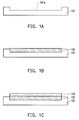
FIG. 1A illustrates a first step of fabricating a substrate structure in accordance with an exemplary embodiment of the present disclosure. -
FIG. 1B illustrates forming a first metal layer on a base in accordance with an exemplary embodiment of the present disclosure. -
FIG. 1C illustrates forming a second metal layer on the first metal layer in accordance with an exemplary embodiment of the present disclosure. -
FIG. 1D illustrates forming a first protective layer on the second metal layer in accordance with an exemplary embodiment of the present disclosure. -
FIG. 1E illustrates patterning the first protective layer in accordance with an exemplary embodiment of the present disclosure. -
FIG. 1F illustrates forming the third metal layer in accordance with an exemplary embodiment of the present disclosure. -
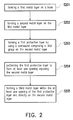
FIG. 2 illustrates a process of fabricating the substrate structure in accordance with an exemplary embodiment of the present disclosure. - Reference will now be made in detail to the present exemplary embodiments of the disclosure, examples of which are illustrated in the accompanying drawings. Wherever possible, the same reference numbers are used in the drawings and the description to refer to the same or like parts.
- The present disclosure proposes a method of fabricating a patterned metal layer structure onto a substrate by using a combination of chemical and laser treatment. The substrate is made of, for example, metal; and in an embodiment of the present disclosure, the metal used for the substrate could be nickel. Under conventional methods, fixtures, equipment, and masks are typically required to cover an area that should not be exposed so as to prevent forming a pattern agent. However, the proposed method does not require masks and associated fixtures and equipment for forming a patterned protective layer. In the proposed method, a protective layer is made of a chemical compound, and at least one opening could be formed in the protective layer, in which the at least one opening can be formed and cleaned by laser, such that the patterned protective layer is formed.
- The patterned protective layer as aforementioned could be formed by a chemical compound known as thiol or a thiol derivative. The thiol compound may have several variants such as Octadecanethiol, Nonanethiol, 1-Hexadecanethiol, 1-Butanethiol, tert-Nonyl mercaptan, Benzyl mercaptan, and Thiophenol. The patterned protective layer could be formed with one or a combination of such variants. The chemical solution that includes thiol or a thiol derivative as aforementioned is referred to as a thiol compound in the present disclosure.
- In one of the exemplary embodiment, the chemical compound that forms the patterned protective layer could be mostly the thiol compound having some non-reactive elements and impurities. The thiol compound is highly flexible during mass production and does not require curing and further processes after curing as required by resins. The thiol compound is laser-able or laser sensitive such that the thiol compound could easily be removed and cleaned by a laser treatment. Also the thiol compound may adhere well to a subsequent layer such as a diffusion barrier layer between metal substrate and metallization solution. For example, the thiol compounds would chemically bind very well with nickel which not only servers as a diffusion barrier layer prevents of metals adhered to the nickel layer but also would prevent oxidation of the nickel layer. Therefore, by applying a general 2D or 3D laser to a chemical protective layer that includes the thiol compound, complex patterns could be developed in the chemical protective layer by forming at least one opening in the chemical protective layer, so that a metal layer could be disposed into the at least one opening of the chemical protective layer by an electroless plating. Such technique would enable a very high rate of production as well as high resolution assuming that a high resolution laser with small spot size is used.
- By using the proposed method, a substrate structure could be developed. The substrate structure would include at least, but not limited to, a base, a first metal layer, a second metal layer, a first protective layer, at least one opening, and a third metal layer. A first metal layer would be disposed on the base. The second metal layer would be disposed on the first metal layer to serve as a diffusion barrier layer and a protective layer. The first protective layer would be made of the thiol compound. By performing a laser etching process, at least one opening could be formed in the first protective layer. In other words, the first protective layer could be patterned and include one or more openings. A third metal layer could be disposed into the at least one opening to be adhered to the second metal layer. The third metal layer could be disposed into the at least one opening via an electroless bath. The substrate structure could be used for a variety of mechanical or electrical structures such as a connector, an antenna, and so forth. However, the substrate structure of present disclosure is not limited to any specific application as the substrate structure could be used for any structures and any applications which require a metal pattern formed on a substrate.
- The proposed method of the present disclosure would have the following advantages. First, the proposed method could form a metal layer having any complex structure or geometry via a laser etching process. Second, all the required equipment, fixture, and electroless bath could easily be obtained in a low cost manner to perform the proposed process which could also be automated for mass production. Third, the proposed method provides a fast production as compared with the conventional method involving photolithography and electroplating. Fourth, the patterned metal layer is only disposed in the at least one opening of the first protective layer, thus a considerable amount of saving could be accomplished. Fifth, it is no longer needed to spray polymeric resin, such as an epoxy, on the second metal layer before curing because the first protective layer could be disposed on the second metal layer by immersion into a solution including the thiol compound. Sixth, when the thiol compound is used as mold to form the patterned metal layer, the dimension of the mold and the subsequently deposited layers would not change because of the formation of the mono-layers of thiol; whereas when a technique involving an application of resin is used, the thickness of the mold would get bigger. Consequently, the changing dimension of the mold and the patterned metal layer could be problematic when the substrate is assembled with other parts.
- An exemplary embodiment is provided by
FIG. 1A∼ FIG. 1F and the corresponding written descriptions of these figures in order to further elucidate the proposed concept. Referring toFIG. 1A , a substrate or a base 101 could be used as a foundation and as a part of a substrate structure. The base 101 could be rigid or flexible. Thebase 101 is, for example, made of polymer; however, the present disclosure is not limited to. In other embodiments of the present disclosure, any metal or non-metal materials could be used as the material of the base 101 as long as thebase 101 is capable of providing adequate stability for the substrate structure and for a subsequent layer to adhere onto. Also according toFIG. 1A , arecess portion 101a is formed in thebase 101 by a laser etching, in which a part of thebase 101 is removed, as such a next metal layer could be disposed into therecess portion 101 a. However, the formation of therecess portion 101a is optional since the next metal layer could also be disposed on a surface of thebase 101 without therecess portion 101a. - Next, a
first metal layer 102 could be formed on a surface of therecess portion 101a of the base 101 as illustrated byFIG. 1B . In the embodiment of the present disclosure, arecess portion 101a is formed in thebase 101 by the laser etching, and thefirst metal layer 102, which could be made of copper for example, is then disposed on the surface of therecess portion 101a of the base 101 by electroplating. For example, the proposed substrate structure is to be used as an antenna, where thefirst metal layer 102 could be copper which serves as a ground for the antenna. However, the use of copper is merely exemplary and should not be construed as a limitation for the present disclosure. Thefirst metal layer 102 could also be made of, for example, gold, silver, or nickel. -
FIG. 1C illustrates the formation of asecond metal layer 103 disposed on thefirst metal layer 102 in accordance with an exemplary embodiment of the present disclosure. Since another metallic layer would eventually be formed as a last metal layer having a pattern, thesecond metal layer 103 would be require to prevent potential diffusion between thefirst metal layer 102 and the last metal layer. Also thesecond metal layer 103 would prevent oxidation of the surfaces of thefirst metal layer 102. Therefore, in the embodiment of the present disclosure, thesecond metal layer 103 is disposed onto thefirst metal layer 102 by an electroless plating. However, a conventional technique, such as electroplating or sputtering, could also be used as long as thesecond metal layer 103 could adhere to thefirst metal layer 102. Thesecond metal layer 103 could be nickel which would serve as an excellent diffusion barrier between two metal layers; however, thesecond metal layer 103 could also be silver or any other materials as long as the materials used as thesecond metal layer 103 could serve as a diffusion barrier and prevent oxidation of the metal layers. - Subsequent to the formation of the
second metal layer 103, a firstprotective layer 104 is disposed on thesecond metal layer 103 as illustrated byFIG. 1D . The firstprotective layer 104 is formed by coating a liquid solution on thesecond metal layer 103, in which the liquid solution includes the thiol or thiol derivative. For one embodiment, the firstprotective layer 104 is formed by a dip coating which thesecond metal layer 103 is inserted and removed from a bath of the liquid solution. If thesecond metal layer 103 is a nickel layer, the liquid solution including the thiol compound would adhere well to nickel. The firstprotective layer 104 would be securely disposed onto thesecond metal layer 103 by placing the uncured firstprotective layer 104 in a room temperature, or placing the firstprotective layer 104 in an oven to expedite the curing process. The firstprotective layer 104 as proposed in the present disclosure would not require an additional step of spraying a polymeric resin, such as an epoxy. The firstprotective layer 104 would serve as a mask, barrier or cover to prevent the last metal layer from being disposed on un-intended locations of thesecond metal layer 103 after the firstprotective layer 104 is patterned. -
FIG. 1E illustrates patterning the firstprotective layer 104 after the firstprotective layer 104 has been securely disposed on thesecond metal layer 103 in accordance with an exemplary embodiment of the present disclosure. Since the thiol compound is sensitive to laser, a general laser process could be performed to pattern the firstprotective layer 104, which at least a portion of the firstprotective layer 104 is removed, and at least oneopening 105 is formed. That is, the firstprotective layer 104 may includes the at least oneopening 105, and which the last metal layer could be disposed into the at least oneopening 105 and further be adhered to thesecond metal layer 103. This process step in FIG. IE could be utilized to replace a process step of photolithography. In this process step, a laser bean is applied to the firstprotective layer 104, which etches away at least a portion of the firstprotective layer 104, thereby forming the at least oneopening 105. The above proposed process step would not require any masks and fixtures to pattern the firstprotective layer 104 for forming the at least oneopening 105. - After the at least one
opening 105 is formed in the firstprotective layer 104,FIG. 1F illustrates a formation of thethird metal layer 106 in accordance with an exemplary embodiment of the present disclosure. Thethird metal layer 106 is formed by disposing a metal layer into the at least oneopening 105. In the embodiment of the present disclosure, thethird metal layer 106 is disposed in the at least oneopening 105 and is located on thesecond metal layer 103 by an electroless plating. Thethird metal layer 106 is, for example, gold. However, the material of thethird metal layer 106 could be, for example, copper, silver, or any other highly conductive metal. - The substrate structure fabricated by the proposed method includes a
base 101, afirst metal layer 102 disposed on thebase 101, asecond metal layer 103 disposed on thefirst metal layer 102, a firstprotective layer 104 made of a chemical solution including a thiol compound and disposed on thesecond metal layer 103, at least oneopening 105 disposed in the firstprotective layer 104 and exposing thesecond metal layer 103, and athird metal layer 106 disposed on thesecond metal layer 103. The firstprotective layer 104 includes at least oneopening 105 exposing thesecond metal layer 103. Thethird metal layer 106 is disposed into the at least oneopening 105 and is disposed on thesecond metal layer 103. -
FIG. 2 is a flow chart which summarizes the process of fabricating the substrate structure in accordance with an exemplary embodiment of the present disclosure. In step S201, a first metal layer is formed on a base. In step S202, a second metal layer is formed on the first metal layer. In step S203, a first protective layer is formed by using a chemical solution including a thiol group on the second metal layer. In step S204, the first protective layer is patterned to form at least one opening exposing the second metal layer. In step S205, a third metal layer is formed within the at least one opening of the first protective layer and is formed directly on the second metal layer. - No element, act, or instruction used in the detailed description of disclosed embodiments of the present application should be construed as absolutely critical or essential to the present disclosure unless explicitly described as such. Also, as used herein, each of the indefinite articles "a" and "an" could include more than one item. If only one item is intended, the terms "a single" or similar languages would be used. Furthermore, the terms "any of" followed by a listing of a plurality of items and/or a plurality of categories of items, as used herein, are intended to include "any of', "any combination of", "any multiple of", and/or "any combination of multiples of the items and/or the categories of items, individually or in conjunction with other items and/or other categories of items. Further, as used herein, the term "set" is intended to include any number of items, including zero. Further, as used herein, the term "number" is intended to include any number, including zero.
Claims (15)
- A method of fabricating a substrate structure comprising:(S201) forming a first metal layer (102) directly on a base (101);(S202) forming a second metal layer (103) directly on the first metal layer (102);(S203) forming a first protective layer (104) by using a compound comprising a thiol group directly on the second metal layer (103);(S204) patterning the first protective layer (104) by laser etching to form at least one opening (105) exposing the second metal layer (103); and(S205) forming a third metal layer (106) within the at least one opening (105) of the first protective layer (104) and directly on the second metal layer (103).
- The method of claim 1, wherein the compound is selected from a group of Octadecanethiol, Nonanethiol, 1-Hexadecanethiol, 1-Butanethiol, tert-Nonyl mercaptan, Benzyl mercaptan, and Thiophenol.
- The method of claim 1, wherein the step (S201) of forming the first metal layer (102) located directly on the base (101) comprises:using a laser to form a recess portion (101a) in the base (101); anddisposing the first metal layer (102) within the recess portion (101a).
- The method of claim 1, wherein the step (S203) of forming the first protective layer (104) comprises:coating a solution of the compound on the second metal layer (103).
- The method of claim 1, wherein the first metal layer (102) is copper or aluminium.
- The method of claim 1, wherein the second metal layer (103) is a diffusion barrier layer which prevents diffusion between the first metal layer (102) and the third metal layer (106) and prevents oxidation of the first metal layer (102); wherein the second metal layer (103) is nickel or silver..
- The method of claim 1, wherein the step (S201) of forming the first metal layer (102) comprises forming the first metal layer (102) directly on the base (101) by an electroless plating.
- The method of claim 1, wherein the step (S205) of forming the third metal layer (106) comprises forming the third metal layer (106) directly on the second metal layer (103) by an electroless plating.
- A substrate structure comprising:a base (101);a first metal layer (102) disposed on the base (101);a second metal layer (103) disposed on the first metal layer (102);a first protective layer (104) made of a thiol compound and disposed on the second metal layer (103) and having at least one opening (105) exposing the second metal layer (103); anda third metal layer (106) disposed within the at least one opening (105) and is disposed on the second metal layer (103).
- The substrate structure of claim 9, wherein the thiol compound is Octadecanethiol.
- The substrate structure of claim 9, wherein the thiol compound is selected from a group of Nonanethiol, 1-Hexadecanethiol, 1-Butanethiol, tert-Nonyl mercaptan, Benzyl mercaptan, and Thiophenol.
- The substrate structure of claim 9, wherein the first metal layer (102) is copper or aluminium.
- The substrate structure of claim 9, wherein the second metal layer (103) is nickel, silver or chromium.
- The substrate structure of claim 9, wherein the base (101) is polymer.
- The substrate structure of claim 9, wherein the third metal layer (106) is gold.
Applications Claiming Priority (1)
| Application Number | Priority Date | Filing Date | Title |
|---|---|---|---|
| US14/265,369 US10087527B2 (en) | 2014-04-30 | 2014-04-30 | Method of fabricating substrate structure and substrate structure fabricated by the same method |
Publications (2)
| Publication Number | Publication Date |
|---|---|
| EP2940528A1 EP2940528A1 (en) | 2015-11-04 |
| EP2940528B1 true EP2940528B1 (en) | 2016-11-16 |
Family
ID=53015659
Family Applications (1)
| Application Number | Title | Priority Date | Filing Date |
|---|---|---|---|
| EP15165648.5A Active EP2940528B1 (en) | 2014-04-30 | 2015-04-29 | Method of fabricating substrate structure and substrate structure fabricated by the same method |
Country Status (4)
| Country | Link |
|---|---|
| US (1) | US10087527B2 (en) |
| EP (1) | EP2940528B1 (en) |
| CN (1) | CN105023848B (en) |
| TW (1) | TWI487443B (en) |
Families Citing this family (5)
| Publication number | Priority date | Publication date | Assignee | Title |
|---|---|---|---|---|
| WO2017188326A1 (en) * | 2016-04-26 | 2017-11-02 | 京セラ株式会社 | Sensor substrate and sensor apparatus |
| CN108231460A (en) * | 2016-12-21 | 2018-06-29 | 深圳市光鼎超导精密技术有限公司 | Electronic product casing is molded the contact manufacturing method that electrically conducts |
| US11404310B2 (en) * | 2018-05-01 | 2022-08-02 | Hutchinson Technology Incorporated | Gold plating on metal layer for backside connection access |
| KR102814782B1 (en) * | 2020-03-12 | 2025-05-30 | 엘지이노텍 주식회사 | Printed circuit board and mehod of manufacturing thereof |
| TWI774206B (en) * | 2021-01-22 | 2022-08-11 | 啟碁科技股份有限公司 | Antenna device |
Family Cites Families (17)
| Publication number | Priority date | Publication date | Assignee | Title |
|---|---|---|---|---|
| US5104480A (en) * | 1990-10-12 | 1992-04-14 | General Electric Company | Direct patterning of metals over a thermally inefficient surface using a laser |
| JPH05226055A (en) * | 1992-02-10 | 1993-09-03 | Nitto Denko Corp | Manufacture of anisotropic conductive film |
| DE19733731A1 (en) * | 1997-08-04 | 1999-02-25 | Siemens Ag | Integrated electrical circuit with passivation layer |
| US6162652A (en) * | 1997-12-31 | 2000-12-19 | Intel Corporation | Process for sort testing C4 bumped wafers |
| US20010033020A1 (en) * | 2000-03-24 | 2001-10-25 | Stierman Roger J. | Structure and method for bond pads of copper-metallized integrated circuits |
| JP2003152014A (en) * | 2001-11-09 | 2003-05-23 | Shinko Electric Ind Co Ltd | Semiconductor device manufacturing method and semiconductor device |
| US6893966B2 (en) * | 2002-11-27 | 2005-05-17 | International Business Machines Corporation | Method of patterning the surface of an article using positive microcontact printing |
| US20050069645A1 (en) * | 2003-05-01 | 2005-03-31 | Johns Hopkins University | Method of electrolytically depositing materials in a pattern directed by surfactant distribution |
| US20080283405A1 (en) * | 2003-05-01 | 2008-11-20 | Johns Hopkins University | Method for Producing Patterned Structures by Printing a Surfactant Resist on a Substrate for Electrodeposition |
| DE102004042169B4 (en) * | 2004-08-31 | 2009-08-20 | Advanced Micro Devices, Inc., Sunnyvale | Technique for increasing the filling capacity in an electrochemical deposition process by rounding the edges and trenches |
| US7883738B2 (en) * | 2007-04-18 | 2011-02-08 | Enthone Inc. | Metallic surface enhancement |
| US7972655B2 (en) * | 2007-11-21 | 2011-07-05 | Enthone Inc. | Anti-tarnish coatings |
| TWI389278B (en) * | 2008-06-19 | 2013-03-11 | 旭德科技股份有限公司 | Package substrate process |
| EP2197253A1 (en) | 2008-12-12 | 2010-06-16 | Nederlandse Organisatie voor toegepast-natuurwetenschappelijk Onderzoek TNO | Method for electric circuit deposition |
| US8552303B2 (en) * | 2011-05-04 | 2013-10-08 | Subtron Technology Co., Ltd. | Circuit structure and manufacturing method thereof |
| TWM410659U (en) * | 2011-05-20 | 2011-09-01 | Chipbond Technology Corp | Bump structure |
| TWM504425U (en) * | 2014-11-14 | 2015-07-01 | 啟碁科技股份有限公司 | Metal pattern structure with positioning layer |
-
2014
- 2014-04-30 US US14/265,369 patent/US10087527B2/en active Active
- 2014-06-23 TW TW103121552A patent/TWI487443B/en active
- 2014-06-27 CN CN201410301559.8A patent/CN105023848B/en active Active
-
2015
- 2015-04-29 EP EP15165648.5A patent/EP2940528B1/en active Active
Also Published As
| Publication number | Publication date |
|---|---|
| CN105023848B (en) | 2017-12-22 |
| US10087527B2 (en) | 2018-10-02 |
| TWI487443B (en) | 2015-06-01 |
| EP2940528A1 (en) | 2015-11-04 |
| CN105023848A (en) | 2015-11-04 |
| US20150315708A1 (en) | 2015-11-05 |
| TW201542052A (en) | 2015-11-01 |
Similar Documents
| Publication | Publication Date | Title |
|---|---|---|
| CN101918617B (en) | Method for manufacturing a metal microstructure and microstructure obtained by this method | |
| EP2940528A1 (en) | Method of fabricating substrate structure and substrate structure fabricated by the same method | |
| US7454832B2 (en) | Method of forming metal plate pattern and circuit board | |
| JP2012505553A (en) | Method for enabling selective substrate area plating | |
| KR20150082406A (en) | Production method for coil element, coil element assembly, and coil component | |
| US20070232051A1 (en) | Method for forming metal bumps | |
| US10224256B2 (en) | Manufacturing method of semiconductor package | |
| US10553456B2 (en) | Semiconductor package and manufacturing method of semiconductor package | |
| US20160043339A1 (en) | Method for producing an electronic component and electronic component | |
| TWI772480B (en) | Method of manufacturing semiconductor package substrate and semiconductor package substrate manufactured using the same | |
| US7168936B2 (en) | Light transparent substrate imprint tool with light blocking distal end | |
| US8296944B2 (en) | Method for manufacturing a printed circuit board | |
| US20130118792A1 (en) | Printed circuit board and method for manufacturing the same | |
| US9461011B2 (en) | Method and apparatus for manufacturing lead frames | |
| US7611985B2 (en) | Formation of holes in substrates using dewetting coatings | |
| US20120124830A1 (en) | Process for fabricating circuit board | |
| US20170358462A1 (en) | Manufacturing method of semiconductor package | |
| US20110067909A1 (en) | Embedded Circuit Board Structure and Fabrication Process Thereof | |
| KR20190077934A (en) | Inductor and Production method of the same | |
| KR20170135357A (en) | A circuit pattern forming method to the metal material | |
| KR101507913B1 (en) | Manufacturing method of printed circuit board | |
| KR101341634B1 (en) | Circuit board used for ball grid array package | |
| Chen et al. | 19, United States i, Patent Application Publication to, Pub. No.: US 2015/0315708A1 | |
| KR20150011510A (en) | A printed circuit board and a method of manufacturing the same | |
| TW201310770A (en) | Portable electronic device and antenna structure and antenna producing process thereof |
Legal Events
| Date | Code | Title | Description |
|---|---|---|---|
| PUAI | Public reference made under article 153(3) epc to a published international application that has entered the european phase |
Free format text: ORIGINAL CODE: 0009012 |
|
| AK | Designated contracting states |
Kind code of ref document: A1 Designated state(s): AL AT BE BG CH CY CZ DE DK EE ES FI FR GB GR HR HU IE IS IT LI LT LU LV MC MK MT NL NO PL PT RO RS SE SI SK SM TR |
|
| AX | Request for extension of the european patent |
Extension state: BA ME |
|
| 17P | Request for examination filed |
Effective date: 20160309 |
|
| RBV | Designated contracting states (corrected) |
Designated state(s): AL AT BE BG CH CY CZ DE DK EE ES FI FR GB GR HR HU IE IS IT LI LT LU LV MC MK MT NL NO PL PT RO RS SE SI SK SM TR |
|
| RIC1 | Information provided on ipc code assigned before grant |
Ipc: B32B 15/04 20060101ALI20160524BHEP Ipc: G03F 7/20 20060101AFI20160524BHEP Ipc: B32B 15/20 20060101ALI20160524BHEP Ipc: H01L 23/06 20060101ALI20160524BHEP Ipc: B32B 3/02 20060101ALI20160524BHEP Ipc: B32B 3/30 20060101ALI20160524BHEP Ipc: H01Q 1/22 20060101ALI20160524BHEP Ipc: B32B 15/08 20060101ALI20160524BHEP Ipc: C23C 18/16 20060101ALI20160524BHEP Ipc: C23C 18/18 20060101ALI20160524BHEP |
|
| GRAP | Despatch of communication of intention to grant a patent |
Free format text: ORIGINAL CODE: EPIDOSNIGR1 |
|
| RAP1 | Party data changed (applicant data changed or rights of an application transferred) |
Owner name: WISTRON NEWEB CORP. |
|
| INTG | Intention to grant announced |
Effective date: 20160722 |
|
| RIN1 | Information on inventor provided before grant (corrected) |
Inventor name: CHEN, CHUN-LIN Inventor name: CHEN, JING-WEN Inventor name: RADI, BABAK Inventor name: KUO, YU-FU Inventor name: CHEN, SHIH-HONG |
|
| GRAS | Grant fee paid |
Free format text: ORIGINAL CODE: EPIDOSNIGR3 |
|
| GRAA | (expected) grant |
Free format text: ORIGINAL CODE: 0009210 |
|
| AK | Designated contracting states |
Kind code of ref document: B1 Designated state(s): AL AT BE BG CH CY CZ DE DK EE ES FI FR GB GR HR HU IE IS IT LI LT LU LV MC MK MT NL NO PL PT RO RS SE SI SK SM TR |
|
| REG | Reference to a national code |
Ref country code: GB Ref legal event code: FG4D |
|
| REG | Reference to a national code |
Ref country code: CH Ref legal event code: EP |
|
| REG | Reference to a national code |
Ref country code: IE Ref legal event code: FG4D |
|
| REG | Reference to a national code |
Ref country code: AT Ref legal event code: REF Ref document number: 846465 Country of ref document: AT Kind code of ref document: T Effective date: 20161215 |
|
| REG | Reference to a national code |
Ref country code: DE Ref legal event code: R096 Ref document number: 602015000721 Country of ref document: DE |
|
| REG | Reference to a national code |
Ref country code: FR Ref legal event code: PLFP Year of fee payment: 3 |
|
| PG25 | Lapsed in a contracting state [announced via postgrant information from national office to epo] |
Ref country code: LV Free format text: LAPSE BECAUSE OF FAILURE TO SUBMIT A TRANSLATION OF THE DESCRIPTION OR TO PAY THE FEE WITHIN THE PRESCRIBED TIME-LIMIT Effective date: 20161116 |
|
| REG | Reference to a national code |
Ref country code: NL Ref legal event code: MP Effective date: 20161116 |
|
| REG | Reference to a national code |
Ref country code: LT Ref legal event code: MG4D |
|
| REG | Reference to a national code |
Ref country code: AT Ref legal event code: MK05 Ref document number: 846465 Country of ref document: AT Kind code of ref document: T Effective date: 20161116 |
|
| PG25 | Lapsed in a contracting state [announced via postgrant information from national office to epo] |
Ref country code: NL Free format text: LAPSE BECAUSE OF FAILURE TO SUBMIT A TRANSLATION OF THE DESCRIPTION OR TO PAY THE FEE WITHIN THE PRESCRIBED TIME-LIMIT Effective date: 20161116 Ref country code: NO Free format text: LAPSE BECAUSE OF FAILURE TO SUBMIT A TRANSLATION OF THE DESCRIPTION OR TO PAY THE FEE WITHIN THE PRESCRIBED TIME-LIMIT Effective date: 20170216 Ref country code: SE Free format text: LAPSE BECAUSE OF FAILURE TO SUBMIT A TRANSLATION OF THE DESCRIPTION OR TO PAY THE FEE WITHIN THE PRESCRIBED TIME-LIMIT Effective date: 20161116 Ref country code: LT Free format text: LAPSE BECAUSE OF FAILURE TO SUBMIT A TRANSLATION OF THE DESCRIPTION OR TO PAY THE FEE WITHIN THE PRESCRIBED TIME-LIMIT Effective date: 20161116 Ref country code: GR Free format text: LAPSE BECAUSE OF FAILURE TO SUBMIT A TRANSLATION OF THE DESCRIPTION OR TO PAY THE FEE WITHIN THE PRESCRIBED TIME-LIMIT Effective date: 20170217 |
|
| PG25 | Lapsed in a contracting state [announced via postgrant information from national office to epo] |
Ref country code: PL Free format text: LAPSE BECAUSE OF FAILURE TO SUBMIT A TRANSLATION OF THE DESCRIPTION OR TO PAY THE FEE WITHIN THE PRESCRIBED TIME-LIMIT Effective date: 20161116 Ref country code: FI Free format text: LAPSE BECAUSE OF FAILURE TO SUBMIT A TRANSLATION OF THE DESCRIPTION OR TO PAY THE FEE WITHIN THE PRESCRIBED TIME-LIMIT Effective date: 20161116 Ref country code: PT Free format text: LAPSE BECAUSE OF FAILURE TO SUBMIT A TRANSLATION OF THE DESCRIPTION OR TO PAY THE FEE WITHIN THE PRESCRIBED TIME-LIMIT Effective date: 20170316 Ref country code: ES Free format text: LAPSE BECAUSE OF FAILURE TO SUBMIT A TRANSLATION OF THE DESCRIPTION OR TO PAY THE FEE WITHIN THE PRESCRIBED TIME-LIMIT Effective date: 20161116 Ref country code: HR Free format text: LAPSE BECAUSE OF FAILURE TO SUBMIT A TRANSLATION OF THE DESCRIPTION OR TO PAY THE FEE WITHIN THE PRESCRIBED TIME-LIMIT Effective date: 20161116 Ref country code: RS Free format text: LAPSE BECAUSE OF FAILURE TO SUBMIT A TRANSLATION OF THE DESCRIPTION OR TO PAY THE FEE WITHIN THE PRESCRIBED TIME-LIMIT Effective date: 20161116 Ref country code: AT Free format text: LAPSE BECAUSE OF FAILURE TO SUBMIT A TRANSLATION OF THE DESCRIPTION OR TO PAY THE FEE WITHIN THE PRESCRIBED TIME-LIMIT Effective date: 20161116 |
|
| PG25 | Lapsed in a contracting state [announced via postgrant information from national office to epo] |
Ref country code: EE Free format text: LAPSE BECAUSE OF FAILURE TO SUBMIT A TRANSLATION OF THE DESCRIPTION OR TO PAY THE FEE WITHIN THE PRESCRIBED TIME-LIMIT Effective date: 20161116 Ref country code: CZ Free format text: LAPSE BECAUSE OF FAILURE TO SUBMIT A TRANSLATION OF THE DESCRIPTION OR TO PAY THE FEE WITHIN THE PRESCRIBED TIME-LIMIT Effective date: 20161116 Ref country code: RO Free format text: LAPSE BECAUSE OF FAILURE TO SUBMIT A TRANSLATION OF THE DESCRIPTION OR TO PAY THE FEE WITHIN THE PRESCRIBED TIME-LIMIT Effective date: 20161116 Ref country code: DK Free format text: LAPSE BECAUSE OF FAILURE TO SUBMIT A TRANSLATION OF THE DESCRIPTION OR TO PAY THE FEE WITHIN THE PRESCRIBED TIME-LIMIT Effective date: 20161116 Ref country code: SK Free format text: LAPSE BECAUSE OF FAILURE TO SUBMIT A TRANSLATION OF THE DESCRIPTION OR TO PAY THE FEE WITHIN THE PRESCRIBED TIME-LIMIT Effective date: 20161116 |
|
| REG | Reference to a national code |
Ref country code: DE Ref legal event code: R097 Ref document number: 602015000721 Country of ref document: DE |
|
| PG25 | Lapsed in a contracting state [announced via postgrant information from national office to epo] |
Ref country code: IT Free format text: LAPSE BECAUSE OF FAILURE TO SUBMIT A TRANSLATION OF THE DESCRIPTION OR TO PAY THE FEE WITHIN THE PRESCRIBED TIME-LIMIT Effective date: 20161116 Ref country code: BG Free format text: LAPSE BECAUSE OF FAILURE TO SUBMIT A TRANSLATION OF THE DESCRIPTION OR TO PAY THE FEE WITHIN THE PRESCRIBED TIME-LIMIT Effective date: 20170216 Ref country code: SM Free format text: LAPSE BECAUSE OF FAILURE TO SUBMIT A TRANSLATION OF THE DESCRIPTION OR TO PAY THE FEE WITHIN THE PRESCRIBED TIME-LIMIT Effective date: 20161116 Ref country code: BE Free format text: LAPSE BECAUSE OF FAILURE TO SUBMIT A TRANSLATION OF THE DESCRIPTION OR TO PAY THE FEE WITHIN THE PRESCRIBED TIME-LIMIT Effective date: 20161116 |
|
| PLBE | No opposition filed within time limit |
Free format text: ORIGINAL CODE: 0009261 |
|
| STAA | Information on the status of an ep patent application or granted ep patent |
Free format text: STATUS: NO OPPOSITION FILED WITHIN TIME LIMIT |
|
| 26N | No opposition filed |
Effective date: 20170817 |
|
| PG25 | Lapsed in a contracting state [announced via postgrant information from national office to epo] |
Ref country code: SI Free format text: LAPSE BECAUSE OF FAILURE TO SUBMIT A TRANSLATION OF THE DESCRIPTION OR TO PAY THE FEE WITHIN THE PRESCRIBED TIME-LIMIT Effective date: 20161116 |
|
| PG25 | Lapsed in a contracting state [announced via postgrant information from national office to epo] |
Ref country code: MC Free format text: LAPSE BECAUSE OF FAILURE TO SUBMIT A TRANSLATION OF THE DESCRIPTION OR TO PAY THE FEE WITHIN THE PRESCRIBED TIME-LIMIT Effective date: 20161116 |
|
| REG | Reference to a national code |
Ref country code: FR Ref legal event code: PLFP Year of fee payment: 4 |
|
| PG25 | Lapsed in a contracting state [announced via postgrant information from national office to epo] |
Ref country code: LU Free format text: LAPSE BECAUSE OF NON-PAYMENT OF DUE FEES Effective date: 20170429 |
|
| PG25 | Lapsed in a contracting state [announced via postgrant information from national office to epo] |
Ref country code: MT Free format text: LAPSE BECAUSE OF NON-PAYMENT OF DUE FEES Effective date: 20170429 |
|
| REG | Reference to a national code |
Ref country code: CH Ref legal event code: PL |
|
| PG25 | Lapsed in a contracting state [announced via postgrant information from national office to epo] |
Ref country code: CH Free format text: LAPSE BECAUSE OF NON-PAYMENT OF DUE FEES Effective date: 20180430 Ref country code: LI Free format text: LAPSE BECAUSE OF NON-PAYMENT OF DUE FEES Effective date: 20180430 |
|
| PG25 | Lapsed in a contracting state [announced via postgrant information from national office to epo] |
Ref country code: HU Free format text: LAPSE BECAUSE OF FAILURE TO SUBMIT A TRANSLATION OF THE DESCRIPTION OR TO PAY THE FEE WITHIN THE PRESCRIBED TIME-LIMIT; INVALID AB INITIO Effective date: 20150429 |
|
| PG25 | Lapsed in a contracting state [announced via postgrant information from national office to epo] |
Ref country code: CY Free format text: LAPSE BECAUSE OF FAILURE TO SUBMIT A TRANSLATION OF THE DESCRIPTION OR TO PAY THE FEE WITHIN THE PRESCRIBED TIME-LIMIT Effective date: 20161116 |
|
| PG25 | Lapsed in a contracting state [announced via postgrant information from national office to epo] |
Ref country code: MK Free format text: LAPSE BECAUSE OF FAILURE TO SUBMIT A TRANSLATION OF THE DESCRIPTION OR TO PAY THE FEE WITHIN THE PRESCRIBED TIME-LIMIT Effective date: 20161116 |
|
| PG25 | Lapsed in a contracting state [announced via postgrant information from national office to epo] |
Ref country code: TR Free format text: LAPSE BECAUSE OF FAILURE TO SUBMIT A TRANSLATION OF THE DESCRIPTION OR TO PAY THE FEE WITHIN THE PRESCRIBED TIME-LIMIT Effective date: 20161116 |
|
| PG25 | Lapsed in a contracting state [announced via postgrant information from national office to epo] |
Ref country code: AL Free format text: LAPSE BECAUSE OF FAILURE TO SUBMIT A TRANSLATION OF THE DESCRIPTION OR TO PAY THE FEE WITHIN THE PRESCRIBED TIME-LIMIT Effective date: 20161116 Ref country code: IS Free format text: LAPSE BECAUSE OF FAILURE TO SUBMIT A TRANSLATION OF THE DESCRIPTION OR TO PAY THE FEE WITHIN THE PRESCRIBED TIME-LIMIT Effective date: 20170316 |
|
| PGFP | Annual fee paid to national office [announced via postgrant information from national office to epo] |
Ref country code: GB Payment date: 20260211 Year of fee payment: 12 |
|
| PGFP | Annual fee paid to national office [announced via postgrant information from national office to epo] |
Ref country code: IE Payment date: 20260210 Year of fee payment: 12 |
|
| PGFP | Annual fee paid to national office [announced via postgrant information from national office to epo] |
Ref country code: FR Payment date: 20260211 Year of fee payment: 12 |
|
| PGFP | Annual fee paid to national office [announced via postgrant information from national office to epo] |
Ref country code: DE Payment date: 20260212 Year of fee payment: 12 |