EP2940527A1 - Photosensitive resin composition, photosensitive film, and method for forming resist pattern - Google Patents
Photosensitive resin composition, photosensitive film, and method for forming resist pattern Download PDFInfo
- Publication number
- EP2940527A1 EP2940527A1 EP13867288.6A EP13867288A EP2940527A1 EP 2940527 A1 EP2940527 A1 EP 2940527A1 EP 13867288 A EP13867288 A EP 13867288A EP 2940527 A1 EP2940527 A1 EP 2940527A1
- Authority
- EP
- European Patent Office
- Prior art keywords
- resin composition
- photosensitive
- photosensitive resin
- component
- compound
- Prior art date
- Legal status (The legal status is an assumption and is not a legal conclusion. Google has not performed a legal analysis and makes no representation as to the accuracy of the status listed.)
- Granted
Links
Images


Classifications
-
- G—PHYSICS
- G03—PHOTOGRAPHY; CINEMATOGRAPHY; ANALOGOUS TECHNIQUES USING WAVES OTHER THAN OPTICAL WAVES; ELECTROGRAPHY; HOLOGRAPHY
- G03F—PHOTOMECHANICAL PRODUCTION OF TEXTURED OR PATTERNED SURFACES, e.g. FOR PRINTING, FOR PROCESSING OF SEMICONDUCTOR DEVICES; MATERIALS THEREFOR; ORIGINALS THEREFOR; APPARATUS SPECIALLY ADAPTED THEREFOR
- G03F7/00—Photomechanical, e.g. photolithographic, production of textured or patterned surfaces, e.g. printing surfaces; Materials therefor, e.g. comprising photoresists; Apparatus specially adapted therefor
- G03F7/004—Photosensitive materials
- G03F7/038—Macromolecular compounds which are rendered insoluble or differentially wettable
- G03F7/0382—Macromolecular compounds which are rendered insoluble or differentially wettable the macromolecular compound being present in a chemically amplified negative photoresist composition
-
- G—PHYSICS
- G03—PHOTOGRAPHY; CINEMATOGRAPHY; ANALOGOUS TECHNIQUES USING WAVES OTHER THAN OPTICAL WAVES; ELECTROGRAPHY; HOLOGRAPHY
- G03F—PHOTOMECHANICAL PRODUCTION OF TEXTURED OR PATTERNED SURFACES, e.g. FOR PRINTING, FOR PROCESSING OF SEMICONDUCTOR DEVICES; MATERIALS THEREFOR; ORIGINALS THEREFOR; APPARATUS SPECIALLY ADAPTED THEREFOR
- G03F7/00—Photomechanical, e.g. photolithographic, production of textured or patterned surfaces, e.g. printing surfaces; Materials therefor, e.g. comprising photoresists; Apparatus specially adapted therefor
- G03F7/004—Photosensitive materials
- G03F7/038—Macromolecular compounds which are rendered insoluble or differentially wettable
- G03F7/0385—Macromolecular compounds which are rendered insoluble or differentially wettable using epoxidised novolak resin
-
- C—CHEMISTRY; METALLURGY
- C08—ORGANIC MACROMOLECULAR COMPOUNDS; THEIR PREPARATION OR CHEMICAL WORKING-UP; COMPOSITIONS BASED THEREON
- C08G—MACROMOLECULAR COMPOUNDS OBTAINED OTHERWISE THAN BY REACTIONS ONLY INVOLVING UNSATURATED CARBON-TO-CARBON BONDS
- C08G59/00—Polycondensates containing more than one epoxy group per molecule; Macromolecules obtained by polymerising compounds containing more than one epoxy group per molecule using curing agents or catalysts which react with the epoxy groups
- C08G59/18—Macromolecules obtained by polymerising compounds containing more than one epoxy group per molecule using curing agents or catalysts which react with the epoxy groups ; e.g. general methods of curing
- C08G59/20—Macromolecules obtained by polymerising compounds containing more than one epoxy group per molecule using curing agents or catalysts which react with the epoxy groups ; e.g. general methods of curing characterised by the epoxy compounds used
- C08G59/22—Di-epoxy compounds
- C08G59/24—Di-epoxy compounds carbocyclic
-
- C—CHEMISTRY; METALLURGY
- C08—ORGANIC MACROMOLECULAR COMPOUNDS; THEIR PREPARATION OR CHEMICAL WORKING-UP; COMPOSITIONS BASED THEREON
- C08G—MACROMOLECULAR COMPOUNDS OBTAINED OTHERWISE THAN BY REACTIONS ONLY INVOLVING UNSATURATED CARBON-TO-CARBON BONDS
- C08G59/00—Polycondensates containing more than one epoxy group per molecule; Macromolecules obtained by polymerising compounds containing more than one epoxy group per molecule using curing agents or catalysts which react with the epoxy groups
- C08G59/18—Macromolecules obtained by polymerising compounds containing more than one epoxy group per molecule using curing agents or catalysts which react with the epoxy groups ; e.g. general methods of curing
- C08G59/40—Macromolecules obtained by polymerising compounds containing more than one epoxy group per molecule using curing agents or catalysts which react with the epoxy groups ; e.g. general methods of curing characterised by the curing agents used
- C08G59/62—Alcohols or phenols
- C08G59/621—Phenols
-
- C—CHEMISTRY; METALLURGY
- C08—ORGANIC MACROMOLECULAR COMPOUNDS; THEIR PREPARATION OR CHEMICAL WORKING-UP; COMPOSITIONS BASED THEREON
- C08G—MACROMOLECULAR COMPOUNDS OBTAINED OTHERWISE THAN BY REACTIONS ONLY INVOLVING UNSATURATED CARBON-TO-CARBON BONDS
- C08G59/00—Polycondensates containing more than one epoxy group per molecule; Macromolecules obtained by polymerising compounds containing more than one epoxy group per molecule using curing agents or catalysts which react with the epoxy groups
- C08G59/18—Macromolecules obtained by polymerising compounds containing more than one epoxy group per molecule using curing agents or catalysts which react with the epoxy groups ; e.g. general methods of curing
- C08G59/68—Macromolecules obtained by polymerising compounds containing more than one epoxy group per molecule using curing agents or catalysts which react with the epoxy groups ; e.g. general methods of curing characterised by the catalysts used
-
- C—CHEMISTRY; METALLURGY
- C08—ORGANIC MACROMOLECULAR COMPOUNDS; THEIR PREPARATION OR CHEMICAL WORKING-UP; COMPOSITIONS BASED THEREON
- C08L—COMPOSITIONS OF MACROMOLECULAR COMPOUNDS
- C08L63/00—Compositions of epoxy resins; Compositions of derivatives of epoxy resins
-
- C—CHEMISTRY; METALLURGY
- C09—DYES; PAINTS; POLISHES; NATURAL RESINS; ADHESIVES; COMPOSITIONS NOT OTHERWISE PROVIDED FOR; APPLICATIONS OF MATERIALS NOT OTHERWISE PROVIDED FOR
- C09D—COATING COMPOSITIONS, e.g. PAINTS, VARNISHES OR LACQUERS; FILLING PASTES; CHEMICAL PAINT OR INK REMOVERS; INKS; CORRECTING FLUIDS; WOODSTAINS; PASTES OR SOLIDS FOR COLOURING OR PRINTING; USE OF MATERIALS THEREFOR
- C09D163/00—Coating compositions based on epoxy resins; Coating compositions based on derivatives of epoxy resins
-
- G—PHYSICS
- G03—PHOTOGRAPHY; CINEMATOGRAPHY; ANALOGOUS TECHNIQUES USING WAVES OTHER THAN OPTICAL WAVES; ELECTROGRAPHY; HOLOGRAPHY
- G03F—PHOTOMECHANICAL PRODUCTION OF TEXTURED OR PATTERNED SURFACES, e.g. FOR PRINTING, FOR PROCESSING OF SEMICONDUCTOR DEVICES; MATERIALS THEREFOR; ORIGINALS THEREFOR; APPARATUS SPECIALLY ADAPTED THEREFOR
- G03F7/00—Photomechanical, e.g. photolithographic, production of textured or patterned surfaces, e.g. printing surfaces; Materials therefor, e.g. comprising photoresists; Apparatus specially adapted therefor
- G03F7/004—Photosensitive materials
-
- G—PHYSICS
- G03—PHOTOGRAPHY; CINEMATOGRAPHY; ANALOGOUS TECHNIQUES USING WAVES OTHER THAN OPTICAL WAVES; ELECTROGRAPHY; HOLOGRAPHY
- G03F—PHOTOMECHANICAL PRODUCTION OF TEXTURED OR PATTERNED SURFACES, e.g. FOR PRINTING, FOR PROCESSING OF SEMICONDUCTOR DEVICES; MATERIALS THEREFOR; ORIGINALS THEREFOR; APPARATUS SPECIALLY ADAPTED THEREFOR
- G03F7/00—Photomechanical, e.g. photolithographic, production of textured or patterned surfaces, e.g. printing surfaces; Materials therefor, e.g. comprising photoresists; Apparatus specially adapted therefor
- G03F7/004—Photosensitive materials
- G03F7/038—Macromolecular compounds which are rendered insoluble or differentially wettable
-
- G—PHYSICS
- G03—PHOTOGRAPHY; CINEMATOGRAPHY; ANALOGOUS TECHNIQUES USING WAVES OTHER THAN OPTICAL WAVES; ELECTROGRAPHY; HOLOGRAPHY
- G03F—PHOTOMECHANICAL PRODUCTION OF TEXTURED OR PATTERNED SURFACES, e.g. FOR PRINTING, FOR PROCESSING OF SEMICONDUCTOR DEVICES; MATERIALS THEREFOR; ORIGINALS THEREFOR; APPARATUS SPECIALLY ADAPTED THEREFOR
- G03F7/00—Photomechanical, e.g. photolithographic, production of textured or patterned surfaces, e.g. printing surfaces; Materials therefor, e.g. comprising photoresists; Apparatus specially adapted therefor
- G03F7/16—Coating processes; Apparatus therefor
-
- G—PHYSICS
- G03—PHOTOGRAPHY; CINEMATOGRAPHY; ANALOGOUS TECHNIQUES USING WAVES OTHER THAN OPTICAL WAVES; ELECTROGRAPHY; HOLOGRAPHY
- G03F—PHOTOMECHANICAL PRODUCTION OF TEXTURED OR PATTERNED SURFACES, e.g. FOR PRINTING, FOR PROCESSING OF SEMICONDUCTOR DEVICES; MATERIALS THEREFOR; ORIGINALS THEREFOR; APPARATUS SPECIALLY ADAPTED THEREFOR
- G03F7/00—Photomechanical, e.g. photolithographic, production of textured or patterned surfaces, e.g. printing surfaces; Materials therefor, e.g. comprising photoresists; Apparatus specially adapted therefor
- G03F7/20—Exposure; Apparatus therefor
-
- G—PHYSICS
- G03—PHOTOGRAPHY; CINEMATOGRAPHY; ANALOGOUS TECHNIQUES USING WAVES OTHER THAN OPTICAL WAVES; ELECTROGRAPHY; HOLOGRAPHY
- G03F—PHOTOMECHANICAL PRODUCTION OF TEXTURED OR PATTERNED SURFACES, e.g. FOR PRINTING, FOR PROCESSING OF SEMICONDUCTOR DEVICES; MATERIALS THEREFOR; ORIGINALS THEREFOR; APPARATUS SPECIALLY ADAPTED THEREFOR
- G03F7/00—Photomechanical, e.g. photolithographic, production of textured or patterned surfaces, e.g. printing surfaces; Materials therefor, e.g. comprising photoresists; Apparatus specially adapted therefor
- G03F7/26—Processing photosensitive materials; Apparatus therefor
- G03F7/30—Imagewise removal using liquid means
- G03F7/32—Liquid compositions therefor, e.g. developers
- G03F7/322—Aqueous alkaline compositions
-
- G—PHYSICS
- G03—PHOTOGRAPHY; CINEMATOGRAPHY; ANALOGOUS TECHNIQUES USING WAVES OTHER THAN OPTICAL WAVES; ELECTROGRAPHY; HOLOGRAPHY
- G03F—PHOTOMECHANICAL PRODUCTION OF TEXTURED OR PATTERNED SURFACES, e.g. FOR PRINTING, FOR PROCESSING OF SEMICONDUCTOR DEVICES; MATERIALS THEREFOR; ORIGINALS THEREFOR; APPARATUS SPECIALLY ADAPTED THEREFOR
- G03F7/00—Photomechanical, e.g. photolithographic, production of textured or patterned surfaces, e.g. printing surfaces; Materials therefor, e.g. comprising photoresists; Apparatus specially adapted therefor
- G03F7/26—Processing photosensitive materials; Apparatus therefor
- G03F7/38—Treatment before imagewise removal, e.g. prebaking
-
- G—PHYSICS
- G03—PHOTOGRAPHY; CINEMATOGRAPHY; ANALOGOUS TECHNIQUES USING WAVES OTHER THAN OPTICAL WAVES; ELECTROGRAPHY; HOLOGRAPHY
- G03F—PHOTOMECHANICAL PRODUCTION OF TEXTURED OR PATTERNED SURFACES, e.g. FOR PRINTING, FOR PROCESSING OF SEMICONDUCTOR DEVICES; MATERIALS THEREFOR; ORIGINALS THEREFOR; APPARATUS SPECIALLY ADAPTED THEREFOR
- G03F7/00—Photomechanical, e.g. photolithographic, production of textured or patterned surfaces, e.g. printing surfaces; Materials therefor, e.g. comprising photoresists; Apparatus specially adapted therefor
- G03F7/26—Processing photosensitive materials; Apparatus therefor
- G03F7/40—Treatment after imagewise removal, e.g. baking
-
- H—ELECTRICITY
- H05—ELECTRIC TECHNIQUES NOT OTHERWISE PROVIDED FOR
- H05K—PRINTED CIRCUITS; CASINGS OR CONSTRUCTIONAL DETAILS OF ELECTRIC APPARATUS; MANUFACTURE OF ASSEMBLAGES OF ELECTRICAL COMPONENTS
- H05K3/00—Apparatus or processes for manufacturing printed circuits
- H05K3/22—Secondary treatment of printed circuits
- H05K3/28—Applying non-metallic protective coatings
- H05K3/285—Permanent coating compositions
- H05K3/287—Photosensitive compositions
-
- H—ELECTRICITY
- H05—ELECTRIC TECHNIQUES NOT OTHERWISE PROVIDED FOR
- H05K—PRINTED CIRCUITS; CASINGS OR CONSTRUCTIONAL DETAILS OF ELECTRIC APPARATUS; MANUFACTURE OF ASSEMBLAGES OF ELECTRICAL COMPONENTS
- H05K3/00—Apparatus or processes for manufacturing printed circuits
- H05K3/46—Manufacturing multilayer circuits
- H05K3/4644—Manufacturing multilayer circuits by building the multilayer layer by layer, i.e. build-up multilayer circuits
- H05K3/4661—Adding a circuit layer by direct wet plating, e.g. electroless plating; insulating materials adapted therefor
-
- H—ELECTRICITY
- H10—SEMICONDUCTOR DEVICES; ELECTRIC SOLID-STATE DEVICES NOT OTHERWISE PROVIDED FOR
- H10P—GENERIC PROCESSES OR APPARATUS FOR THE MANUFACTURE OR TREATMENT OF DEVICES COVERED BY CLASS H10
- H10P14/00—Formation of materials, e.g. in the shape of layers or pillars
- H10P14/60—Formation of materials, e.g. in the shape of layers or pillars of insulating materials
- H10P14/68—Organic materials, e.g. photoresists
- H10P14/683—Organic materials, e.g. photoresists carbon-based polymeric organic materials, e.g. polyimides, poly cyclobutene or PVC
-
- H—ELECTRICITY
- H10—SEMICONDUCTOR DEVICES; ELECTRIC SOLID-STATE DEVICES NOT OTHERWISE PROVIDED FOR
- H10P—GENERIC PROCESSES OR APPARATUS FOR THE MANUFACTURE OR TREATMENT OF DEVICES COVERED BY CLASS H10
- H10P50/00—Etching of wafers, substrates or parts of devices
- H10P50/20—Dry etching; Plasma etching; Reactive-ion etching
- H10P50/28—Dry etching; Plasma etching; Reactive-ion etching of insulating materials
-
- H—ELECTRICITY
- H05—ELECTRIC TECHNIQUES NOT OTHERWISE PROVIDED FOR
- H05K—PRINTED CIRCUITS; CASINGS OR CONSTRUCTIONAL DETAILS OF ELECTRIC APPARATUS; MANUFACTURE OF ASSEMBLAGES OF ELECTRICAL COMPONENTS
- H05K1/00—Printed circuits
- H05K1/02—Details
- H05K1/03—Use of materials for the substrate
- H05K1/0313—Organic insulating material
- H05K1/0353—Organic insulating material consisting of two or more materials, e.g. two or more polymers, polymer + filler, + reinforcement
Definitions
- the present invention relates to a photosensitive resin composition, a photosensitive film, and a method for forming a resist pattern.
- photosensitive resin compositions are widely used in various semiconductors and in microfabrication.
- the photosensitive resin composition on a substrate is exposed to active rays and subjected to a proper treatment with a developer for selective removal of exposed portions or unexposed portions so as to form a resist pattern.
- optical processing is achieved by inducing changes in solubility of the photosensitive resin composition.
- the photosensitive resin composition may be either one of a positive type or a negative type, and the exposure with active rays is performed to increase or decrease the solubility in the developer, depending on the use.
- Patent Literatures 1 and 3 materials including a combination of an acrylic photo-curing agent and an epoxy heat-curing agent have been used as the material system.
- a photosensitive resin composition containing a novolac resin, an epoxy resin, and a photo-acid generator is disclosed in Patent Literatures 1 and 3, and a photosensitive resin composition containing an alkali-soluble epoxy compound having a carboxyl group and a photo-cationic polymerization initiator is disclosed in Patent Literature 4.
- Patent Literature 2 a photosensitive resin composition relating to a surface protective film or an interlayer insulating film of a semiconductor is described in Patent Literature 2.
- Patent Literature 1 JPH9-087366
- Patent Literature 2 JP2003-215802
- Patent Literature 3 JP2007-522531
- Patent Literature 4 WO 2008/010521
- a photosensitive resin composition is, therefore, required to be excellent in photosensitive properties, heat resistance, electrical properties, mechanical properties, etc.
- the photosensitive resin compositions described in the Citation List are excellent in insulation reliability, etc., a high resolution cannot be achieved when a thick film is made therefrom.
- the photosensitive resin composition described in Patent Literature 1 provides a resolution with a space width of only about 40 ⁇ m when a coating film has a thickness of 50 ⁇ m.
- the photosensitive resin composition described in Patent Literature 2 provides an excellent resolution with a space width of about 5 ⁇ m when a coating film has a thickness of 10 ⁇ m, but no satisfactory resolution can be obtained when a thick film is made therefrom.
- An object of the present invention is to solve the above problems associated with the conventional arts and to provide a photosensitive resin composition excellent in the resolution and the heat resistance, even when a coating film having a thickness of more than 20 ⁇ m is formed. Further, another object of the present invention is to provide a cured product (insulating film) obtained by curing the photosensitive resin composition.
- the photosensitive resin composition of the present invention comprises: (A) a resin having a phenolic hydroxyl group; (B) an aliphatic or alicyclic epoxy compound having two or more oxirane rings; (C) a photosensitive acid generator; and (D) a solvent; wherein the photosensitive resin composition comprises 20 to 70 parts by mass of the component (B) relative to 100 parts by mass of the component (A).
- the component (B) preferably has two or more glycidyl ether groups, and more preferably has three or more glycidyl ether groups.
- the present invention also provides a photosensitive film comprising a substrate and a photosensitive layer of the photosensitive resin composition formed on the substrate.
- the present invention further provides a cured product of the above described photosensitive resin composition.
- the cured product can be preferably used as a solder resist or an interlayer insulating film.
- the present invention provides a method for forming a resist pattern comprising: a step of applying the photosensitive resin composition onto a substrate and drying the applied photosensitive resin composition so as to form a photosensitive layer, a step of exposing the photosensitive layer to an active ray so as to form a predetermined pattern and performing a heat-treatment after exposure (hereinafter, this heat-treatment is also referred to as "post-exposure baking"), and a step of developing the photosensitive layer after heat-treatment and heat-treating the obtained resin pattern.
- the present invention further provides a method for forming a resist pattern comprising: a step of forming the photosensitive layer of the photosensitive film on a substrate, a step of exposing the photosensitive layer to an active ray so as to form a predetermined pattern and performing a post-exposure heat-treatment, and a step of developing the photosensitive layer after heat-treatment and heat-treating the obtained resin pattern.
- a photosensitive resin composition to form a resist pattern having a high aspect ratio (defined as "height of an image formed/width of an image formed") is required.
- the photosensitive resin composition of the present invention allows a resist pattern having a high aspect ratio with excellent resolution and heat resistance to be formed, even when a coating film having a thickness more than 20 ⁇ m is formed.
- the photosensitive resin composition of the present embodiment comprises: (A) a resin having a phenolic hydroxyl group; (B) an aliphatic or alicyclic epoxy compound having two or more oxirane rings; (C) a photosensitive acid generator; and (D) a solvent.
- the photosensitive resin composition of the present embodiment may comprise: (E) a cross-linking agent; (F) a sensitizer; and the like, if necessary.
- the present inventors presume the reason that a resin pattern having a high aspect ratio can be formed from the photosensitive resin composition of the present embodiment is as follows. First, the solubility of (A) the resin having a phenolic hydroxyl group in a developer is drastically improved with addition of the component (B) in unexposed portions. Second, due to the acid generated from (C) the photosensitive acid generator, not only the cross-linking resulting from the reaction of two or more oxirane rings of the component (B), but also the reaction of them with the phenolic hydroxyl group of the component (A) occur, so that the solubility of the composition in the developer is drastically reduced in exposed portions.
- the present inventors presume that the difference in solubility in a developer between unexposed portions and exposed portions becomes thereby pronounced when developed, so that sufficient resolution can be obtained; and presume that due to the heat treatment of the developed pattern, the cross-linking of the component (B) and the reaction of it with the component (A) further proceed, so that a resin pattern having sufficient heat resistance can be obtained.
- Examples of the resin having a phenolic hydroxyl group as component (A) preferably include a resin soluble in an alkali aqueous solution, particularly preferably a novolac resin, though not specifically limited.
- the novolac resin can be obtained from condensation of phenols and aldehydes under presence of a catalyst.
- phenols examples include phenol, o-cresol, m-cresol, p-cresol, o-ethylphenol, m-ethylphenol, p-ethylphenol, o-butylphenol, m-butylphenol, p-butylphenol, 2,3-xylenol, 2,4-xylenol, 2,5-xylenol, 2,6-xylenol, 3,4-xylenol, 3,5-xylenol, 2,3,5-trimethylphenol, 3,4,5-trimethylphenol, catechol, resorcinol, pyrogallol, ⁇ -naphthol, ⁇ -naphthol, etc.
- aldehydes examples include formaldehyde, paraformaldehyde, acetaldehyde, benzaldehyde, etc.
- the novolac resin examples include a phenol/formaldehyde condensation novolac resin, a cresol/formaldehyde condensation novolac resin, a phenol-naphthol/formaldehyde condensation novolac resin, etc.
- examples of the component (A) other than novolac resins include polyhydroxystyrene and a copolymer thereof, a phenol-xylylene glycol condensation resin, a cresol-xylylene glycol condensation resin, a phenol-dicyclopentadiene condensate resin, etc.
- a single kind of the component (A) or a mixture of two or more kinds of the components (A) may be used.
- the component (A) has a weight average molecular weight of preferably 100000 or less, more preferably 1000 to 80000, furthermore preferably 2000 to 50000, particularly preferably 2000 to 20000, extremely preferably 5000 to 15000.
- the photosensitive resin composition of the present embodiment has a content of component (A) of, preferably 30 to 90 parts by mass, more preferably 40 to 80 parts by mass, relative to 100 parts by mass in total of the photosensitive resin composition except for the component (D). With a proportion of the component (A) in the above range, the film formed from the photosensitive resin composition to be obtained has more excellent developability in an alkali aqueous solution.
- the aliphatic or alicyclic epoxy compound having two or more oxirane rings as component (B) is preferably an epoxy compound having a weight average molecular weight of preferably 1000 or less. Further, the component (B) is preferably a compound having two or more glycidyl ether groups, more preferably a compound having three or more glycidyl ether groups.
- the term "aliphatic or alicyclic epoxy compound” means a compound having an aliphatic skeleton and/or an alicyclic skeleton as the main skeleton, having no aromatic or heterocyclic ring.
- component (B) examples include ethylene glycol diglycidyl ether, diethylene glycol diglycidyl ether, propylene glycol diglycidyl ether, tripropylene glycol diglycidyl ether, neopentyl glycol diglycidyl ether, 1,6-hexanediol diglycidyl ether, glycerol diglycidyl ether, pentaerythritol tetraglycidyl ether, trimethylol ethane triglycidyl ether, trimethylolpropane triglycidyl ether, glycerol propoxylate triglycidyl ether, dicyclopentadiene dioxide, 1,2,5,6-diepoxycyclooctane, 1,4-cyclohexanedimethanol diglycidyl ether, diglycidyl 1,2-cyclohexane dicarboxylate, 3,4-epoxycyclohexan
- trimethylolethane triglycidyl ether or trimethylolpropane triglycidyl ether is preferred, in terms of the excellent sensitivity and resolution.
- Examples of the commercially available component (B) include EPOLIGHT 40E, EPOLIGHT 100E, EPOLIGHT 70P, EPOLIGHT 200P, EPOLIGHT 1500NP, EPOLIGHT 1600, EPOLIGHT 80MF, and EPOLIGHT 100MF (all the above are made by Kyoeisha Chemical Co., Ltd., trade names), an alkyl-type epoxy resin ZX-1542 (made by Nippon Steel and Sumikin Chemical Co., Ltd., trade name), DENACOL EX-212L, DENACOL EX-214L, DENACOL EX-216L, DENACOL EX-321L, and DENACOL EX-850L (all the above made by Nagase ChemteX Corporation, trade names).
- a single kind of the component (B) or a mixture of two or more kinds of the components (B) may be used.
- the content of component (B) is 20 to 70 parts by mass, preferably 25 to 65 parts by mass, more preferably 35 to 55 parts by mass, relative to the 100 parts by mass of the component (A).
- a content of component (B) of 20 parts by mass or more the resolution tends to be more easily improved due to sufficient cross-linking in exposed portions.
- a content of 70 parts by mass or less film formation of the photosensitive resin composition can be easily performed on a desired substrate and the resolution tends to hardly decrease.
- the photosensitive acid generator as component (C) is a compound which generates an acid upon irradiation with active rays or the like. Due to the acid generated, not only the cross-linking of the component (B) to each other, but also the reaction of the component (B) with the phenolic hydroxyl group of the component (A) occur, so that the solubility of the composition in the developer decreases drastically.
- the component (C) is not specifically limited as long as being a compound which generates an acid with irradiation of active rays, and examples thereof include an onium salt compound, a halogen-containing compound, a diazoketone compound, a sulfone compound, a sulfonic acid compound, a sulfonimide compound, and a diazomethane compound, etc.
- an onium salt compound a compound which generates an acid with irradiation of active rays
- a sulfonimide compound or an onium salt compound is preferred from the viewpoint of easier availability.
- use of an onium salt compound is preferred from the viewpoint of solubility in the component (F) as solvent.
- the component (C) is preferably a compound having a trifluoromethanesulfonate group, a hexafluoroantimonate group, a hexafluorophosphate group, or a tetrafluoroborate group, in terms of having excellent sensitivity and resolution.
- a single kind of the component (C) or a mixture of two or more kinds of the components (C) may be used.
- the content of the component (C) is preferably 0.1 to 15 parts by mass, more preferably 0.3 to 10 parts by mass, relative to 100 parts by mass of the component (A), from the viewpoint of ensuring the sensitivity, the resolution, the pattern shape and the like of the photosensitive resin composition of the present embodiment.
- the solvent as component (D) is added to improve the handling properties of the photosensitive resin composition, or to control the viscosity and the storage stability.
- the component (D) is preferably an organic solvent.
- the kind of the organic solvent is not specifically limited as long as capable of exhibiting the performance above-mentioned, and examples thereof include ethylene glycol monoalkyl ether acetates such as ethylene glycol monomethyl ether acetate and ethylene glycol monoethyl ether acetate; propylene glycol monoalkyl ethers such as propylene glycol monomethyl ether, propylene glycol monoethyl ether, propylene glycol monopropyl ether, and propylene glycol monobutyl ether; propylene glycol dialkyl ethers such as propylene glycol dimethyl ether, propylene glycol diethyl ether, propylene glycol dipropyl ether, and propylene glycol dibutyl ether; propylene glycol monoalkyl
- the content of the component (D) is preferably 30 to 200 parts by mass, more preferably 60 to 120 parts by mass, relative to 100 parts by mass of the total amount of the photosensitive resin composition except for the component (D).
- the photosensitive resin composition of the present embodiment may further comprise a cross-linking agent as component (E), if necessary.
- a cross-linking agent as component (E)
- Inclusion of the component (E) prevents the resin pattern from being embrittled and deformed when the photosensitive layer is cured by heating after formation of the resin pattern, due to formation of a cross-linked structure resulting from the reaction of the component (E) with the component (A).
- component (E) for use examples include a compound having a phenolic hydroxyl group (though excluding the component (A)) and a compound having a hydroxymethylamino group.
- a single kind of the component (E) or a mixture of two or more kinds of the components (E) may be used.
- the "compound having a phenolic hydroxyl group" for use as component (E) preferably further includes a methylol group or an alkoxyalkyl group.
- the compound having a phenolic hydroxyl group as component (E) increases the dissolution rate of unexposed portions in development in an alkali aqueous solution and improves the sensitivity.
- the weight average molecular weight of the compound having a phenolic hydroxyl group is preferably 2000 or less. In view of the balance among the solubility in an alkali aqueous solution, the photosensitivity, and the mechanical properties, the number average molecular weight is preferably 94 to 2000, more preferably 108 to 2000, furthermore preferably 108 to 1500.
- a conventionally known compound may be the "compound having a phenolic hydroxyl group" for use as component (E)
- use of a compound represented by the following formula (1) is preferred due to excellent balance between the effect of enhancing dissolution of unexposed portions and the effect of preventing deformation of the resin pattern after curing by heating: wherein Z represents a single bond or a divalent organic group, R 1 and R 2 each independently represent a hydrogen atom or a monovalent organic group, R 3 and R 4 each independently represent a monovalent organic group, a and b each independently represent an integer of 1 to 3, and c and d each independently represent an integer of 0 to 3.
- the compound with a single bond as Z in the formula (1) is a biphenol (dihydroxy biphenyl) derivative.
- examples of the divalent organic group represented by Z include: an alkylene group having 1 to 10 carbon atoms such as a methylene group, an ethylene group, and a propylene group; an alkylidene group having 2 to 10 carbon atoms such as an ethylidene group; an arylene group having 6 to 30 carbon atoms such as a phenylene group; a group having any of these hydrocarbon groups with a part or the whole of hydrogen atoms being substituted with halogen atoms such as fluorine atoms; a sulfonyl group; a carbonyl group; an ether bond; a sulfide bond; an amide bond; etc.
- Z is preferably a divalent organic group represented by the following formula (2): wherein X represents a single bond, an alkylene group (e.g. an alkylene group having 1 to 10 carbon atoms), an alkylidene group (e.g.
- R 5 represents a hydrogen atom, a hydroxyl group, an alkyl group, or a haloalkyl group
- e represents an integer of 1 to 10
- a plurality of R 5 may be the same or different from each other.
- Examples of the compound having a hydroxymethylamino group include a nitrogen-containing compound having methylol groups partially or totally alkyl-etherified such as (poly)(N-hydroxymethyl)melamine, (poly)(N-hydroxymethyl)glycoluril, (poly)(N-hydroxymethyl)benzoguanamine, (poly)(N-hydroxymethyl)urea, etc.
- Examples of the alkyl group of an alkyl ether include a methyl group, an ethyl group, a butyl group, and a mixture thereof, and also these compounds may contain an oligomer component formed by partial self-condensation.
- Specific examples thereof include hexakis(methoxymethyl)melamine, hexakis(butoxymethyl)melamine, tetrakis(methoxymethyl)glycoluril, tetrakis(butoxymethyl)glycoluril, tetrakis(methoxymethyl)urea, etc.
- the content of component (E) is preferably 5 to 50 parts by mass, more preferably 5 to 30 parts by mass, relative to 100 parts by mass of the component (A).
- the photosensitive resin composition of the present embodiment may further comprise a sensitizer as component (F), if necessary.
- a sensitizer as component (F)
- Inclusion of the component (F) can improve the sensitivity of the photosensitive resin composition.
- the sensitizer include 9,10-dibutoxyanthracene, etc.
- a single kind of the component (F) or a mixture of two or more kinds of the components (F) may be used.
- the content of the component (F) is preferably 0.01 to 1.5 parts by mass, more preferably 0.05 to 0.5 parts by mass, relative to 100 parts by mass of the component (A)
- the photosensitive resin composition of the present embodiment may further comprise a low-molecular weight phenolic compound having a molecular weight less than 1000 (hereinafter referred to as "phenol compound (a)") in addition to the component (A).
- phenol compound (a) a low-molecular weight phenolic compound having a molecular weight less than 1000
- examples thereof include 4,4'-dihydroxydiphenylmethane, 4,4'-dihydroxydiphenyl ether, tris(4-hydroxyphenyl)methane, 1,1-bis(4-hydroxyphenyl)-1-phenylethane, tris(4-hydroxyphenyl)ethane, 1,3-bis[1-(4-hydroxyphenyl)-1-methylethyl]benzene, 1,4-bis[1-(4-hydroxyphenyl)-1-methylethyl]benzene, 4,6-bis[1-(4-hydroxyphenyl)-1-methylethyl]-1,3-dihydroxybenz
- the photosensitive resin composition of the present embodiment may comprise other components other than the above components.
- the other component include an inorganic filler, an adhesion aid, a leveling agent, etc.
- the photosensitive film of the present embodiment will be described in the following.
- the photosensitive film of the present embodiment comprises a substrate and a photosensitive layer of the above-described photosensitive resin composition formed on the substrate.
- a protective layer for covering the photosensitive layer may be further provided on the photosensitive layer.
- Examples of the above-described substrate for use include a polymer film of polyethylene terephthalate, polypropylene, polyethylene, polyester, or the like, having heat resistance and solvent resistance.
- the thickness of the substrate (polymer film) is preferably set to 5 to 25 ⁇ m.
- the polymer films for use may be laminated on both sides of a photosensitive layer, including one as substrate and another as protective film.
- Examples of the above-described protective film for use include a polymer film of polyethylene terephthalate, polypropylene, polyethylene, polyester, or the like, having heat resistance and solvent resistance.
- the photosensitive layer may be formed by applying the photosensitive resin composition on a substrate or a protective film.
- the coating method include dipping, spraying, bar coating, roll coating, spin coating, etc.
- the thickness of the photosensitive layer is different depending on the use, the dried photosensitive layer has a thickness of preferably 10 to 100 ⁇ m, more preferably 15 to 60 ⁇ m, particularly preferably 20 to 50 ⁇ m.
- a photosensitive layer made from the above-described photosensitive resin composition is formed on a substrate (a copper foil coated with a resin, a copper-clad laminate, a silicon wafer coated with a metal-sputtered film, an alumina substrate, etc.) on which a resist is to be formed.
- a substrate a copper foil coated with a resin, a copper-clad laminate, a silicon wafer coated with a metal-sputtered film, an alumina substrate, etc.
- the method for forming the photosensitive layer include: a method of applying the photosensitive resin composition to a substrate and drying to evaporate the solvent and the like so as to form a coating film (photosensitive layer); and a method of transferring the photosensitive layer of the above-described photosensitive film onto a substrate; etc.
- Examples of the method for use in applying the photosensitive resin composition to a substrate include an application method such as dipping, spraying, bar coating, roll coating, spin coating, etc.
- the thickness of the coating film can be appropriately controlled by adjusting the coating means, and the solid content and viscosity of the photosensitive resin composition.
- the photosensitive layer is exposed to an active ray through a predetermined mask so as to form a predetermined pattern.
- the active ray for use in exposure include rays for use in a g-line stepper; ultraviolet rays for use in a low pressure mercury lamp, a high pressure mercury lamp, a metal halide lamp, and an i-line stepper; electron beams; laser beams; etc.
- the exposure dose is appropriately selected according to the light source for use and the thickness of a coating film, and the like, and may be, for example, about 1000 to 20000 J/m 2 for a coating film thickness of 10 to 50 ⁇ m with ultraviolet irradiation from a high pressure mercury lamp.
- a heat treatment is performed after exposure (post-exposure baking).
- the post-exposure baking can accelerate the curing reaction between the component (A) and the component (B) due to the generated acid.
- the conditions for the post-exposure baking are different depending on the content of the photosensitive resin composition, the thickness of the coating film, and the like, heating at 70 to 150°C for about 1 to 60 minutes is typically preferred, and heating at 80 to 120°C for about 1 to 60 minutes is more preferred
- the coating film after subjected to post-exposure baking is developed in alkali developer, so that regions other than photo-cured portions (unexposed portions) are dissolved and removed to obtain a desired resin pattern.
- Examples of the development method in this case include shower developing, spray developing, dip developing, paddle developing, etc. Typical development conditions are at 20 to 40°C for about 1 to 10 minutes.
- the alkali developer examples include an alkali aqueous solution containing an alkali compound such as sodium hydroxide, potassium hydroxide, tetramethylammonium hydroxide, choline, etc., dissolved in water at a concentration of about 1 to 10 mass%, an alkali aqueous solution such as an aqueous ammonia solution, etc.
- a water soluble organic solvent such as methanol and ethanol, a surfactant, or the like in an appropriate amount may be added to the alkali aqueous solution.
- Tetramethylammonium hydroxide is preferred as alkali developer, in terms of achieving excellent resolution.
- a cured film (resist pattern) is obtained.
- Curing conditions of the photosensitive resin composition are not specifically limited, so that the photosensitive resin composition can be cured by heating at 50 to 200°C for about 30 minutes to 10 hours, depending on the use of the cured product.
- the heat treatment may be performed in two stages for sufficient progress of curing and prevention of deformation of the obtained shape of a resin pattern.
- curing may be performed by heating at 50 to 120°C for about 5 minutes to 2 hours in a first stage, and at 80 to 200°C for about 10 minutes to 10 hours in a second stage.
- Heating facilities are not specifically limited as long as the above-described conditions are satisfied, so that an oven in common use, an infrared furnace, etc., may be used.
- FIG. 1 is a schematic view illustrating the manufacturing method of a multi-layer printed wiring board which comprises the cured product formed from the photosensitive resin composition of the present embodiment as a solder resist and/or an interlayer insulating film.
- the multi-layer printed wiring board 100A shown in Figure 1(f) has wiring patterns on the surface and on the inside.
- the multi-layer printed wiring board 100A is obtained by stacking a copper-clad laminate, an interlayer insulating film, and a metal foil, etc., and appropriately forming wiring patterns by etching or a semi-additive method.
- the manufacturing method of a multi-layer printed wiring board 100A is briefly described in the following with reference to Figure 1 .
- interlayer insulating films 103 are respectively formed on both sides of the copper-clad laminate 101 having a wiring pattern 102 on the surface (refer to Figure 1(a) ).
- the interlayer insulating films 103 may be formed by printing with a screen printing machine or a roll coater using the photosensitive resin composition, or by previously preparing the photosensitive film and sticking the photosensitive layer of the photosensitive film to the surface of a printed wiring board with a laminater.
- an orifices 104 are formed at portions required to be electrically connected to the outside with YAG laser or carbon dioxide laser (refer to Figure 1(b) ). Smears (residues) around the orifices 104 are removed by a desmearing treatment.
- a seed layer 105 is formed by electroless plating (refer to Figure 1(c) ).
- a photosensitive layer formed from the above-described photosensitive resin composition is laminated on the seed layer 105, and predetermined portions are subjected to exposure and developing treatment so as to form a wiring pattern 106 (refer to Figure 1(d) ).
- a wiring pattern 107 is formed by electrolytic plating, and the cured product of the photosensitive resin composition is removed with a stripping solution.
- the seed layer 105 is then removed by etching (refer to Figure 1(e) ).
- the above-described operations are repeated, so that a solder resist 108 formed of the cured product of the photosensitive resin composition is formed on the outermost surface. Consequently the multi-layer printed wiring board 100A can be thus formed (refer to Figure 1(f) ).
- the thus obtained multi-layer printed wiring board 100A allows the semiconductor elements mounted at corresponding positions to have ensured electrical connection.
- a resin composition was obtained by mixing 100 parts by mass of novolac resin (A-1), 43 parts by mass of an epoxy compound (B-1 to B-7 and B'-8 to B'-13), and 100 parts by mass of a solvent (D-1).
- a 6-inch silicon wafer was spin-coated with the resin composition, which was heated at 65°C for 2 minutes and then at 95°C for 8 minutes on a hot plate, so that a uniform coating film having a thickness of 25 ⁇ m was prepared.
- the prepared coating film was immersed in 2.38 mass% tetramethylammonium hydroxide aqueous solution at 23°C in a Petri dish, and the complete dissolution time was measured.
- the dissolution rate (nm/sec) was calculated from (film thickness after film formation)/(complete dissolution time). Further, the solubility was evaluated according to the following criteria. The evaluation results are shown in Table 1.
- Reference Examples 1 to 7 had better solubility in an alkali aqueous solution with an improved dissolution rate in comparison with Reference Example 8 which did not comprise component (B).
- Reference Examples 9 to 14 to which an epoxy compound other than the component (B) was added had a lowered dissolving rate, and Reference Examples 10 to 14 had a lowered solubility in an alkali aqueous solution.
- a photosensitive resin composition was obtained by blending predetermined amounts of an epoxy compound (B-1 to B-7 and B'-8 to B'-10), a photosensitive acid generator (C-1), a solvent (D-1), and a sensitizer (F-1) shown in Table 2 with 100 parts by mass of a novolac resin (A-1 to A-3).
- a 6-inch silicon wafer was spin-coated with the photosensitive resin composition, which was heated at 65°C for 2 minutes and then at 95°C for 8 minutes on a hot plate, so that a uniform coating film having a thickness of 25 ⁇ m was prepared.
- the prepared coating film was subjected to reduced projection exposure to i-line (wavelength: 365 nm) through a mask by using an i-line stepper (made by Canon Inc., trade name: FPA-3000iW).
- the mask for use had patterns with a ratio of exposed portions to unexposed portions of 1:1 at 1 ⁇ m intervals from 2 ⁇ m:2 ⁇ m to 30 ⁇ m:30 ⁇ m. Further, reduction projection exposure was performed with changing the exposure dose at an interval of 50 mJ/cm 2 in the range of 50 to 950 mJ/cm 2 .
- the exposed coating film was heated at 65°C for 1 minute and then at 95°C for 4 minutes (post-exposure baking), and then immersed in 2.38 mass% tetramethylammonium hydroxide aqueous solution for a time period 1.5 times the minimum developing time period (minimum time period for removal of unexposed portions) for development, and unexposed portions were removed in the developing treatment.
- the formed resist pattern was observed with a metallurgical microscope.
- the smallest space width of the resin patterns having clearly removed space portions (unexposed portions) and line portions (exposed portions) formed without occurrence of meandering or chipping was assumed to be the minimum resolution, and the exposure dose on that occasion was evaluated. The evaluation results are shown in Table 2.
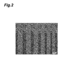
- Figure 2 is a metallurgical microscope photograph showing a resin pattern formed from the photosensitive resin composition in Example 4.
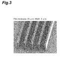
- Figure 3 is a scanning electron microscope photograph showing a resin pattern formed from the photosensitive resin composition in Example 4.
- Figure 4 is a metallurgical microscope photograph showing a resin pattern formed from the photosensitive resin composition in Comparative Example 3.
- the space portions were clearly removed and a resin pattern having a resolution of 5 ⁇ m was formed.
- the photosensitive resin composition in Comparative Example 3 the formed resin pattern accompanied meandering and detachment, having a resolution of 14 ⁇ m.
- Example 4 the photosensitive resin composition in Example 4 was uniformly applied on a polyethylene terephthalate film (made by Teijin DuPont Films Ltd., trade name: PUREX A53), and dried at 90°C for 10 minutes with a hot air convection dryer, so that a dried photosensitive layer having a thickness of 40 ⁇ m was formed. Subsequently, the photosensitive layer was exposed to have an irradiation energy of 400 mJ/cm 2 with an exposure machine having a high-pressure mercury lamp (made by ORC Manufacturing Co., Ltd., trade name: EXM-1201).
- the exposed photosensitive layer was heated at 65°C for 2 minutes and then at 95°C for 8 minutes on a hot plate, subjected to a heat treatment at 180°C for 60 minutes with a hot air convection dryer, and then peeled from the polyethylene terephthalate film so as to obtain a cured film.
- a thermomechanical analyzer made by Seiko Instruments Inc., trade name: TMA/SS6000
- TMA/SS6000 thermomechanical analyzer
- Examples 1 to 10 had an exposure dose required for curing of 800 mJ/cm 2 or less, a minimum resolution of 9 or less, and excellent heat resistance.
- Comparative Examples 1 to 3 and 7 not containing an aliphatic or alicyclic epoxy compound having 2 or more oxirane rings had a higher exposure dose required for curing and a larger minimum resolution in comparison with Examples 1 to 10.
- Examples 4, 5, 9, and 10 containing 20 to 70 parts by mass of the component (B) relative to 100 parts by mass of component (A) had a more excellent balance among the exposure dose required for curing, the resolution, and the heat resistance, in comparison with Comparative Examples 4 to 6.
- the photosensitive resin composition of the present invention is applied as a material for use in a solder resist or an interlayer insulating film of a wiring board material, or a surface protective film (overcoat film) or an interlayer insulating film (passivation film) of a semiconductor device or the like.
- the photosensitive resin composition is suitably used for a high-density package substrate having thinned wiring and high density.
- 100A MULTI-LAYER PRINTED WIRING BOARD; 101: COPPER-CLAD LAMINATE; 102, 106, AND 107: WIRING PATTERN; 103: INTERLAYER INSULATING FILM; 104: ORIFICE; 105: SEED LAYER; 108: SOLDER RESIST
Landscapes
- Chemical & Material Sciences (AREA)
- Physics & Mathematics (AREA)
- Engineering & Computer Science (AREA)
- General Physics & Mathematics (AREA)
- Organic Chemistry (AREA)
- Chemical Kinetics & Catalysis (AREA)
- Polymers & Plastics (AREA)
- Health & Medical Sciences (AREA)
- Medicinal Chemistry (AREA)
- Microelectronics & Electronic Packaging (AREA)
- Spectroscopy & Molecular Physics (AREA)
- Manufacturing & Machinery (AREA)
- Life Sciences & Earth Sciences (AREA)
- Materials Engineering (AREA)
- Wood Science & Technology (AREA)
- Materials For Photolithography (AREA)
- Exposure And Positioning Against Photoresist Photosensitive Materials (AREA)
- Non-Metallic Protective Coatings For Printed Circuits (AREA)
- Production Of Multi-Layered Print Wiring Board (AREA)
- Organic Low-Molecular-Weight Compounds And Preparation Thereof (AREA)
Abstract
Description
- The present invention relates to a photosensitive resin composition, a photosensitive film, and a method for forming a resist pattern.
- Currently, photosensitive resin compositions are widely used in various semiconductors and in microfabrication. In these applications, the photosensitive resin composition on a substrate is exposed to active rays and subjected to a proper treatment with a developer for selective removal of exposed portions or unexposed portions so as to form a resist pattern. During the treatment, optical processing is achieved by inducing changes in solubility of the photosensitive resin composition. The photosensitive resin composition may be either one of a positive type or a negative type, and the exposure with active rays is performed to increase or decrease the solubility in the developer, depending on the use.
- Conventionally, materials including a combination of an acrylic photo-curing agent and an epoxy heat-curing agent have been used as the material system. For example, a photosensitive resin composition containing a novolac resin, an epoxy resin, and a photo-acid generator is disclosed in
Patent Literatures 1 and 3, and a photosensitive resin composition containing an alkali-soluble epoxy compound having a carboxyl group and a photo-cationic polymerization initiator is disclosed inPatent Literature 4. Further, a photosensitive resin composition relating to a surface protective film or an interlayer insulating film of a semiconductor is described in Patent Literature 2. - Patent Literature 1:
JPH9-087366 - Patent Literature 2:
JP2003-215802 - Patent Literature 3:
JP2007-522531 - Patent Literature 4:
WO 2008/010521 - With speeding-up of electronic devices, the densification of a wiring board material has proceeded year by year. As a result, microfabrication of a solder resist and an interlayer insulating film for a wiring board has been also increasingly required. A photosensitive resin composition is, therefore, required to be excellent in photosensitive properties, heat resistance, electrical properties, mechanical properties, etc. However, although the photosensitive resin compositions described in the Citation List are excellent in insulation reliability, etc., a high resolution cannot be achieved when a thick film is made therefrom. For example, the photosensitive resin composition described in Patent Literature 1 provides a resolution with a space width of only about 40 µm when a coating film has a thickness of 50 µm. Further, the photosensitive resin composition described in Patent Literature 2 provides an excellent resolution with a space width of about 5 µm when a coating film has a thickness of 10 µm, but no satisfactory resolution can be obtained when a thick film is made therefrom.
- An object of the present invention is to solve the above problems associated with the conventional arts and to provide a photosensitive resin composition excellent in the resolution and the heat resistance, even when a coating film having a thickness of more than 20 µm is formed. Further, another object of the present invention is to provide a cured product (insulating film) obtained by curing the photosensitive resin composition.
- As a result of extensive studies to solve the above problems, the present inventors have found a photosensitive resin composition having excellent properties. Namely, the photosensitive resin composition of the present invention comprises: (A) a resin having a phenolic hydroxyl group; (B) an aliphatic or alicyclic epoxy compound having two or more oxirane rings; (C) a photosensitive acid generator; and (D) a solvent; wherein the photosensitive resin composition comprises 20 to 70 parts by mass of the component (B) relative to 100 parts by mass of the component (A).
- The component (B) preferably has two or more glycidyl ether groups, and more preferably has three or more glycidyl ether groups.
- The present invention also provides a photosensitive film comprising a substrate and a photosensitive layer of the photosensitive resin composition formed on the substrate.
- The present invention further provides a cured product of the above described photosensitive resin composition. The cured product can be preferably used as a solder resist or an interlayer insulating film.
- The present invention provides a method for forming a resist pattern comprising: a step of applying the photosensitive resin composition onto a substrate and drying the applied photosensitive resin composition so as to form a photosensitive layer, a step of exposing the photosensitive layer to an active ray so as to form a predetermined pattern and performing a heat-treatment after exposure (hereinafter, this heat-treatment is also referred to as "post-exposure baking"), and a step of developing the photosensitive layer after heat-treatment and heat-treating the obtained resin pattern.
- The present invention further provides a method for forming a resist pattern comprising: a step of forming the photosensitive layer of the photosensitive film on a substrate, a step of exposing the photosensitive layer to an active ray so as to form a predetermined pattern and performing a post-exposure heat-treatment, and a step of developing the photosensitive layer after heat-treatment and heat-treating the obtained resin pattern.
- In applications involving the fabrication of advanced electronic packages requiring high density interconnectors, a photosensitive resin composition to form a resist pattern having a high aspect ratio (defined as "height of an image formed/width of an image formed") is required. The photosensitive resin composition of the present invention allows a resist pattern having a high aspect ratio with excellent resolution and heat resistance to be formed, even when a coating film having a thickness more than 20 µm is formed.
-
-
Figure 1 is a schematic view illustrating the manufacturing method of a multi-layer printed wiring board in an embodiment of the present invention. -
Figure 2 is a metallurgical microscope photograph showing a resin pattern formed from the photosensitive resin composition in Example 4. -
Figure 3 is a scanning electron microscope photograph showing a resin pattern formed from the photosensitive resin composition in Example 4. -
Figure 4 is a metallurgical microscope photograph showing a resin pattern formed from the photosensitive resin composition in Comparative Example 3. - An embodiment of the present invention will be more specifically described in the following, though the present invention is not limited thereto.
- The photosensitive resin composition of the present embodiment comprises: (A) a resin having a phenolic hydroxyl group; (B) an aliphatic or alicyclic epoxy compound having two or more oxirane rings; (C) a photosensitive acid generator; and (D) a solvent. The photosensitive resin composition of the present embodiment may comprise: (E) a cross-linking agent; (F) a sensitizer; and the like, if necessary.
- The present inventors presume the reason that a resin pattern having a high aspect ratio can be formed from the photosensitive resin composition of the present embodiment is as follows. First, the solubility of (A) the resin having a phenolic hydroxyl group in a developer is drastically improved with addition of the component (B) in unexposed portions. Second, due to the acid generated from (C) the photosensitive acid generator, not only the cross-linking resulting from the reaction of two or more oxirane rings of the component (B), but also the reaction of them with the phenolic hydroxyl group of the component (A) occur, so that the solubility of the composition in the developer is drastically reduced in exposed portions. The present inventors presume that the difference in solubility in a developer between unexposed portions and exposed portions becomes thereby pronounced when developed, so that sufficient resolution can be obtained; and presume that due to the heat treatment of the developed pattern, the cross-linking of the component (B) and the reaction of it with the component (A) further proceed, so that a resin pattern having sufficient heat resistance can be obtained.
- Examples of the resin having a phenolic hydroxyl group as component (A) preferably include a resin soluble in an alkali aqueous solution, particularly preferably a novolac resin, though not specifically limited. The novolac resin can be obtained from condensation of phenols and aldehydes under presence of a catalyst.
- Examples of the phenols include phenol, o-cresol, m-cresol, p-cresol, o-ethylphenol, m-ethylphenol, p-ethylphenol, o-butylphenol, m-butylphenol, p-butylphenol, 2,3-xylenol, 2,4-xylenol, 2,5-xylenol, 2,6-xylenol, 3,4-xylenol, 3,5-xylenol, 2,3,5-trimethylphenol, 3,4,5-trimethylphenol, catechol, resorcinol, pyrogallol, α-naphthol, β-naphthol, etc.
- Further, examples of the aldehydes include formaldehyde, paraformaldehyde, acetaldehyde, benzaldehyde, etc.
- Specific examples of the novolac resin include a phenol/formaldehyde condensation novolac resin, a cresol/formaldehyde condensation novolac resin, a phenol-naphthol/formaldehyde condensation novolac resin, etc.
- Further, examples of the component (A) other than novolac resins include polyhydroxystyrene and a copolymer thereof, a phenol-xylylene glycol condensation resin, a cresol-xylylene glycol condensation resin, a phenol-dicyclopentadiene condensate resin, etc. A single kind of the component (A) or a mixture of two or more kinds of the components (A) may be used.
- From the viewpoints of the resolution, developability, thermal shock, heat resistance, etc., of a cured film to be obtained, the component (A) has a weight average molecular weight of preferably 100000 or less, more preferably 1000 to 80000, furthermore preferably 2000 to 50000, particularly preferably 2000 to 20000, extremely preferably 5000 to 15000.
- The photosensitive resin composition of the present embodiment has a content of component (A) of, preferably 30 to 90 parts by mass, more preferably 40 to 80 parts by mass, relative to 100 parts by mass in total of the photosensitive resin composition except for the component (D). With a proportion of the component (A) in the above range, the film formed from the photosensitive resin composition to be obtained has more excellent developability in an alkali aqueous solution.
- The aliphatic or alicyclic epoxy compound having two or more oxirane rings as component (B) is preferably an epoxy compound having a weight average molecular weight of preferably 1000 or less. Further, the component (B) is preferably a compound having two or more glycidyl ether groups, more preferably a compound having three or more glycidyl ether groups. In the present specification, the term "aliphatic or alicyclic epoxy compound" means a compound having an aliphatic skeleton and/or an alicyclic skeleton as the main skeleton, having no aromatic or heterocyclic ring.
- Examples of the component (B) include ethylene glycol diglycidyl ether, diethylene glycol diglycidyl ether, propylene glycol diglycidyl ether, tripropylene glycol diglycidyl ether, neopentyl glycol diglycidyl ether, 1,6-hexanediol diglycidyl ether, glycerol diglycidyl ether, pentaerythritol tetraglycidyl ether, trimethylol ethane triglycidyl ether, trimethylolpropane triglycidyl ether, glycerol propoxylate triglycidyl ether, dicyclopentadiene dioxide, 1,2,5,6-diepoxycyclooctane, 1,4-cyclohexanedimethanol diglycidyl ether, diglycidyl 1,2-cyclohexane dicarboxylate, 3,4-epoxycyclohexylmethyl 3',4'-epoxycyclohexane carboxylate, bis(3,4-epoxycyclohexylmethyl) adipate, and cyclohexene oxide-type epoxy resin, etc.
- Among the components (B), trimethylolethane triglycidyl ether or trimethylolpropane triglycidyl ether is preferred, in terms of the excellent sensitivity and resolution.
- Examples of the commercially available component (B) include EPOLIGHT 40E, EPOLIGHT 100E, EPOLIGHT 70P, EPOLIGHT 200P, EPOLIGHT 1500NP, EPOLIGHT 1600, EPOLIGHT 80MF, and EPOLIGHT 100MF (all the above are made by Kyoeisha Chemical Co., Ltd., trade names), an alkyl-type epoxy resin ZX-1542 (made by Nippon Steel and Sumikin Chemical Co., Ltd., trade name), DENACOL EX-212L, DENACOL EX-214L, DENACOL EX-216L, DENACOL EX-321L, and DENACOL EX-850L (all the above made by Nagase ChemteX Corporation, trade names). A single kind of the component (B) or a mixture of two or more kinds of the components (B) may be used.
- In the photosensitive resin composition of the present embodiment, the content of component (B) is 20 to 70 parts by mass, preferably 25 to 65 parts by mass, more preferably 35 to 55 parts by mass, relative to the 100 parts by mass of the component (A). With a content of component (B) of 20 parts by mass or more, the resolution tends to be more easily improved due to sufficient cross-linking in exposed portions. With a content of 70 parts by mass or less, film formation of the photosensitive resin composition can be easily performed on a desired substrate and the resolution tends to hardly decrease.
- The photosensitive acid generator as component (C) is a compound which generates an acid upon irradiation with active rays or the like. Due to the acid generated, not only the cross-linking of the component (B) to each other, but also the reaction of the component (B) with the phenolic hydroxyl group of the component (A) occur, so that the solubility of the composition in the developer decreases drastically.
- The component (C) is not specifically limited as long as being a compound which generates an acid with irradiation of active rays, and examples thereof include an onium salt compound, a halogen-containing compound, a diazoketone compound, a sulfone compound, a sulfonic acid compound, a sulfonimide compound, and a diazomethane compound, etc. Among them, use of a sulfonimide compound or an onium salt compound is preferred from the viewpoint of easier availability. In particular, use of an onium salt compound is preferred from the viewpoint of solubility in the component (F) as solvent.
- Onium salt compound:
- Examples of the onium salt compound include an iodonium salt, a sulfonium salt, a phosphonium salt, a diazonium salt and a pyridinium salt. Specific preferred examples of the onium salt compound include a diaryliodonium salt such as a diphenyliodonium trifluoromethanesulfonate, diphenyliodonium p-toluenesulfonate, diphenyliodonium hexafluoroantimonate, diphenyliodonium hexafluorophosphate, diphenyliodonium tetrafluoroborate; a triarylsulfonium salt such as triphenylsulfonium trifluoromethanesulfonate, triphenylsulfonium p-toluenesulfonate, and triphenylsulfonium hexafluoroantimonate; 4-t-butylphenyl-diphenysulfonium trifluoromethanesulfonate; 4-t-butylphenyl-diphenylsulfonium p-toluenesulfonate; and 4,7-di-n-butoxynaphthyl tetrahydrothiophenium trifluoromethanesulfonate.
- Halogen-containing compound:
- Examples of the halogen-containing compound include a haloalkyl group-containing hydrocarbon compound and a haloalkyl group-containing heterocyclic compound. Specific preferred examples of the halogen-containing compound include 1,10-dibromo-n-decane, 1,1-bis(4-chlorophenyl)-2,2,2-trichloroethane; and an s-triazine derivative such as phenyl-bis(trichloromethyl)-s-triazine, 4-methoxyphenyl-bis(trichloromethyl)-s-triazine, styryl-bis(trichloromethyl)-s-triazine, and naphthyl-bis(trichloromethyl)-s-triazine.
- Diazoketone compound:
- Examples of the diazoketone compound include a 1,3-diketo-2-diazo compound, a diazobenzoquinone compound, and a diazonaphthoquinone compound. Specific examples thereof include a 1,2-naphthoquinonediazide-4-sulfonic acid ester compound of phenols.
- Sulfone compound:
- Examples of the sulfone compound include a β-ketosulfone compound, a β-sulfonylsulfone compound, and an α-diazo compound thereof. Specific examples thereof include 4-tolylphenacylsulfone, mesitylphenacylsulfone, bis(phenacylsulfonyl)methane, etc.
- Sulfonic acid compound:
- Examples of the sulfonic acid compound include alkylsulfonates, haloalkylsulfonates, arylsulfonates, iminosulfonates, etc. Specific preferred examples thereof include benzoin p-toluenesulfonate, pyrogallol tris-trifluoromethanesulfonate, o-nitrobenzyl trifluoromethanesulfonate, o-nitrobenzyl p-toluenesulfonate, etc.
- Sulfonimide compound:
- Specific examples of the sulfonimide compound include N-(trifluoromethylsulfonyloxy)succinimide, N-(trifluoromethylsulfonyloxy)phthalimide, N-(trifluoromethylsulfonyloxy)diphenylmaleimide, N-(trifluoromethylsulfonyloxy)bicyclo[2.2.1]hept-5-ene-2,3-dicarboxim ide, N-(trifluoromethylsulfonyloxy)naphthalimide, N-(p-toluenesulfonyloxy)-1,8-naphthalimide, N-(10-camphorsulfonyloxy)-1,8-naphthalimide, etc.
- Diazomethane compound:
- Specific examples of the diazomethane compound include bis(trifluoromethylsulfonyl)diazomethane, bis(cyclohexylsulfonyl)diazomethane, and bis(phenylsulfonyl)diazomethane.
- In the present embodiment, the component (C) is preferably a compound having a trifluoromethanesulfonate group, a hexafluoroantimonate group, a hexafluorophosphate group, or a tetrafluoroborate group, in terms of having excellent sensitivity and resolution. Incidentally, a single kind of the component (C) or a mixture of two or more kinds of the components (C) may be used.
- In the photosensitive resin composition of the present embodiment, the content of the component (C) is preferably 0.1 to 15 parts by mass, more preferably 0.3 to 10 parts by mass, relative to 100 parts by mass of the component (A), from the viewpoint of ensuring the sensitivity, the resolution, the pattern shape and the like of the photosensitive resin composition of the present embodiment.
- The solvent as component (D) is added to improve the handling properties of the photosensitive resin composition, or to control the viscosity and the storage stability. The component (D) is preferably an organic solvent. The kind of the organic solvent is not specifically limited as long as capable of exhibiting the performance above-mentioned, and examples thereof include ethylene glycol monoalkyl ether acetates such as ethylene glycol monomethyl ether acetate and ethylene glycol monoethyl ether acetate; propylene glycol monoalkyl ethers such as propylene glycol monomethyl ether, propylene glycol monoethyl ether, propylene glycol monopropyl ether, and propylene glycol monobutyl ether; propylene glycol dialkyl ethers such as propylene glycol dimethyl ether, propylene glycol diethyl ether, propylene glycol dipropyl ether, and propylene glycol dibutyl ether; propylene glycol monoalkyl ether acetates such as propylene glycol monomethyl ether acetate, propylene glycol monoethyl ether acetate, propylene glycol monopropyl ether acetate, and propylene glycol monobutyl ether acetate; cellosolves such as ethyl cellosolve and butyl cellosolve, carbitols such as butyl carbitol; lactates such as methyl lactate, ethyl lactate, n-propyl lactate, and isopropyl lactate; aliphatic carboxylic acid esters such as ethyl acetate, n-propyl acetate, isopropyl acetate, n-butyl acetate, isobutyl acetate, n-amyl acetate, isoamyl acetate, isopropyl propionate, n-butyl propionate and isobutyl propionate; other esters such as 3-methoxy methyl propionate, 3-methoxy ethyl propionate, 3-ethoxy methyl propionate, 3-ethoxy ethyl propionate, methyl pyruvate, and ethyl pyruvate; aromatic hydrocarbons such as toluene and xylene; ketones such as 2-butanone, 2-heptanone, 3-heptanone, 4-heptanone, and cyclohexanone; amides such as N,N-dimethylformamide, N-methylacetamide, N,N-dimethylacetamide, and N-methylpyrrolidone; and lactones such as γ-butyrolactone. A single kind of the organic solvent or a mixture of two or more kinds of the organic solvents may be used.
- In the photosensitive resin composition of the present embodiment, the content of the component (D) is preferably 30 to 200 parts by mass, more preferably 60 to 120 parts by mass, relative to 100 parts by mass of the total amount of the photosensitive resin composition except for the component (D).
- The photosensitive resin composition of the present embodiment may further comprise a cross-linking agent as component (E), if necessary. Inclusion of the component (E) prevents the resin pattern from being embrittled and deformed when the photosensitive layer is cured by heating after formation of the resin pattern, due to formation of a cross-linked structure resulting from the reaction of the component (E) with the component (A).
- Specific preferred examples of the component (E) for use include a compound having a phenolic hydroxyl group (though excluding the component (A)) and a compound having a hydroxymethylamino group. A single kind of the component (E) or a mixture of two or more kinds of the components (E) may be used.
- The "compound having a phenolic hydroxyl group" for use as component (E) preferably further includes a methylol group or an alkoxyalkyl group. The compound having a phenolic hydroxyl group as component (E) increases the dissolution rate of unexposed portions in development in an alkali aqueous solution and improves the sensitivity. The weight average molecular weight of the compound having a phenolic hydroxyl group is preferably 2000 or less. In view of the balance among the solubility in an alkali aqueous solution, the photosensitivity, and the mechanical properties, the number average molecular weight is preferably 94 to 2000, more preferably 108 to 2000, furthermore preferably 108 to 1500.
- Although a conventionally known compound may be the "compound having a phenolic hydroxyl group" for use as component (E), use of a compound represented by the following formula (1) is preferred due to excellent balance between the effect of enhancing dissolution of unexposed portions and the effect of preventing deformation of the resin pattern after curing by heating:

- The compound with a single bond as Z in the formula (1) is a biphenol (dihydroxy biphenyl) derivative. Further, examples of the divalent organic group represented by Z include: an alkylene group having 1 to 10 carbon atoms such as a methylene group, an ethylene group, and a propylene group; an alkylidene group having 2 to 10 carbon atoms such as an ethylidene group; an arylene group having 6 to 30 carbon atoms such as a phenylene group; a group having any of these hydrocarbon groups with a part or the whole of hydrogen atoms being substituted with halogen atoms such as fluorine atoms; a sulfonyl group; a carbonyl group; an ether bond; a sulfide bond; an amide bond; etc. Among these, Z is preferably a divalent organic group represented by the following formula (2):

- Examples of the compound having a hydroxymethylamino group include a nitrogen-containing compound having methylol groups partially or totally alkyl-etherified such as (poly)(N-hydroxymethyl)melamine, (poly)(N-hydroxymethyl)glycoluril, (poly)(N-hydroxymethyl)benzoguanamine, (poly)(N-hydroxymethyl)urea, etc. Examples of the alkyl group of an alkyl ether include a methyl group, an ethyl group, a butyl group, and a mixture thereof, and also these compounds may contain an oligomer component formed by partial self-condensation. Specific examples thereof include hexakis(methoxymethyl)melamine, hexakis(butoxymethyl)melamine, tetrakis(methoxymethyl)glycoluril, tetrakis(butoxymethyl)glycoluril, tetrakis(methoxymethyl)urea, etc.
- In the photosensitive resin composition of the present embodiment, the content of component (E) is preferably 5 to 50 parts by mass, more preferably 5 to 30 parts by mass, relative to 100 parts by mass of the component (A).
- The photosensitive resin composition of the present embodiment may further comprise a sensitizer as component (F), if necessary. Inclusion of the component (F) can improve the sensitivity of the photosensitive resin composition. Examples of the sensitizer include 9,10-dibutoxyanthracene, etc. A single kind of the component (F) or a mixture of two or more kinds of the components (F) may be used.
- In the photosensitive resin composition of the present embodiment, the content of the component (F) is preferably 0.01 to 1.5 parts by mass, more preferably 0.05 to 0.5 parts by mass, relative to 100 parts by mass of the component (A)
- The photosensitive resin composition of the present embodiment may further comprise a low-molecular weight phenolic compound having a molecular weight less than 1000 (hereinafter referred to as "phenol compound (a)") in addition to the component (A). Examples thereof include 4,4'-dihydroxydiphenylmethane, 4,4'-dihydroxydiphenyl ether, tris(4-hydroxyphenyl)methane, 1,1-bis(4-hydroxyphenyl)-1-phenylethane, tris(4-hydroxyphenyl)ethane, 1,3-bis[1-(4-hydroxyphenyl)-1-methylethyl]benzene, 1,4-bis[1-(4-hydroxyphenyl)-1-methylethyl]benzene, 4,6-bis[1-(4-hydroxyphenyl)-1-methylethyl]-1,3-dihydroxybenzene, 1,1-bis(4-hydroxyphenyl)-1-[4-{1-(4-hydroxyphenyl)-1-methylethyl}ph enyl]ethane, 1,1,2,2-tetra(4-hydroxyphenyl)ethane, etc. These phenol compounds (a) can be contained in the range of 0 to 40 mass%, particularly 0 to 30 mass%, relative to the component (A).
- The photosensitive resin composition of the present embodiment may comprise other components other than the above components. Examples of the other component include an inorganic filler, an adhesion aid, a leveling agent, etc.
- The photosensitive film of the present embodiment will be described in the following.
- The photosensitive film of the present embodiment comprises a substrate and a photosensitive layer of the above-described photosensitive resin composition formed on the substrate. A protective layer for covering the photosensitive layer may be further provided on the photosensitive layer.
- Examples of the above-described substrate for use include a polymer film of polyethylene terephthalate, polypropylene, polyethylene, polyester, or the like, having heat resistance and solvent resistance. The thickness of the substrate (polymer film) is preferably set to 5 to 25 µm. The polymer films for use may be laminated on both sides of a photosensitive layer, including one as substrate and another as protective film.
- Examples of the above-described protective film for use include a polymer film of polyethylene terephthalate, polypropylene, polyethylene, polyester, or the like, having heat resistance and solvent resistance.
- The photosensitive layer may be formed by applying the photosensitive resin composition on a substrate or a protective film. Examples of the coating method include dipping, spraying, bar coating, roll coating, spin coating, etc. Although the thickness of the photosensitive layer is different depending on the use, the dried photosensitive layer has a thickness of preferably 10 to 100 µm, more preferably 15 to 60 µm, particularly preferably 20 to 50 µm.
- The method for forming a resist pattern of the present embodiment is described below.
- First, a photosensitive layer made from the above-described photosensitive resin composition is formed on a substrate (a copper foil coated with a resin, a copper-clad laminate, a silicon wafer coated with a metal-sputtered film, an alumina substrate, etc.) on which a resist is to be formed. Examples of the method for forming the photosensitive layer include: a method of applying the photosensitive resin composition to a substrate and drying to evaporate the solvent and the like so as to form a coating film (photosensitive layer); and a method of transferring the photosensitive layer of the above-described photosensitive film onto a substrate; etc.
- Examples of the method for use in applying the photosensitive resin composition to a substrate include an application method such as dipping, spraying, bar coating, roll coating, spin coating, etc. The thickness of the coating film can be appropriately controlled by adjusting the coating means, and the solid content and viscosity of the photosensitive resin composition.
- Subsequently, the photosensitive layer is exposed to an active ray through a predetermined mask so as to form a predetermined pattern. Examples of the active ray for use in exposure include rays for use in a g-line stepper; ultraviolet rays for use in a low pressure mercury lamp, a high pressure mercury lamp, a metal halide lamp, and an i-line stepper; electron beams; laser beams; etc. The exposure dose is appropriately selected according to the light source for use and the thickness of a coating film, and the like, and may be, for example, about 1000 to 20000 J/m2 for a coating film thickness of 10 to 50 µm with ultraviolet irradiation from a high pressure mercury lamp.
- Further, a heat treatment is performed after exposure (post-exposure baking). The post-exposure baking can accelerate the curing reaction between the component (A) and the component (B) due to the generated acid. Although the conditions for the post-exposure baking are different depending on the content of the photosensitive resin composition, the thickness of the coating film, and the like, heating at 70 to 150°C for about 1 to 60 minutes is typically preferred, and heating at 80 to 120°C for about 1 to 60 minutes is more preferred
- Subsequently, the coating film after subjected to post-exposure baking is developed in alkali developer, so that regions other than photo-cured portions (unexposed portions) are dissolved and removed to obtain a desired resin pattern. Examples of the development method in this case include shower developing, spray developing, dip developing, paddle developing, etc. Typical development conditions are at 20 to 40°C for about 1 to 10 minutes.
- Examples of the alkali developer include an alkali aqueous solution containing an alkali compound such as sodium hydroxide, potassium hydroxide, tetramethylammonium hydroxide, choline, etc., dissolved in water at a concentration of about 1 to 10 mass%, an alkali aqueous solution such as an aqueous ammonia solution, etc. A water soluble organic solvent such as methanol and ethanol, a surfactant, or the like in an appropriate amount may be added to the alkali aqueous solution. After development with the alkali developer, washing with water and drying are performed. Tetramethylammonium hydroxide is preferred as alkali developer, in terms of achieving excellent resolution.
- Further, through a heat treatment for imparting insulating film properties, a cured film (resist pattern) is obtained. Curing conditions of the photosensitive resin composition are not specifically limited, so that the photosensitive resin composition can be cured by heating at 50 to 200°C for about 30 minutes to 10 hours, depending on the use of the cured product.
- Further, the heat treatment may be performed in two stages for sufficient progress of curing and prevention of deformation of the obtained shape of a resin pattern. For example, curing may be performed by heating at 50 to 120°C for about 5 minutes to 2 hours in a first stage, and at 80 to 200°C for about 10 minutes to 10 hours in a second stage.
- Heating facilities are not specifically limited as long as the above-described conditions are satisfied, so that an oven in common use, an infrared furnace, etc., may be used.
- The cured product formed from the photosensitive resin composition of the present embodiment can be suitably used as a solder resist and/or an interlayer insulating film in a multi-layer printed wiring board.
Figure 1 is a schematic view illustrating the manufacturing method of a multi-layer printed wiring board which comprises the cured product formed from the photosensitive resin composition of the present embodiment as a solder resist and/or an interlayer insulating film. The multi-layer printedwiring board 100A shown inFigure 1(f) has wiring patterns on the surface and on the inside. The multi-layer printedwiring board 100A is obtained by stacking a copper-clad laminate, an interlayer insulating film, and a metal foil, etc., and appropriately forming wiring patterns by etching or a semi-additive method. The manufacturing method of a multi-layer printedwiring board 100A is briefly described in the following with reference toFigure 1 . - First,
interlayer insulating films 103 are respectively formed on both sides of the copper-cladlaminate 101 having awiring pattern 102 on the surface (refer toFigure 1(a) ). Theinterlayer insulating films 103 may be formed by printing with a screen printing machine or a roll coater using the photosensitive resin composition, or by previously preparing the photosensitive film and sticking the photosensitive layer of the photosensitive film to the surface of a printed wiring board with a laminater. Subsequently, anorifices 104 are formed at portions required to be electrically connected to the outside with YAG laser or carbon dioxide laser (refer toFigure 1(b) ). Smears (residues) around theorifices 104 are removed by a desmearing treatment. Subsequently, aseed layer 105 is formed by electroless plating (refer toFigure 1(c) ). A photosensitive layer formed from the above-described photosensitive resin composition is laminated on theseed layer 105, and predetermined portions are subjected to exposure and developing treatment so as to form a wiring pattern 106 (refer toFigure 1(d) ). Subsequently, awiring pattern 107 is formed by electrolytic plating, and the cured product of the photosensitive resin composition is removed with a stripping solution. Theseed layer 105 is then removed by etching (refer toFigure 1(e) ). The above-described operations are repeated, so that a solder resist 108 formed of the cured product of the photosensitive resin composition is formed on the outermost surface. Consequently the multi-layer printedwiring board 100A can be thus formed (refer toFigure 1(f) ). - The thus obtained multi-layer printed
wiring board 100A allows the semiconductor elements mounted at corresponding positions to have ensured electrical connection. - The present invention will be illustrated in detail with reference to Examples and Comparative Examples as follows, but the present invention is not limited to the Examples in any way. In the following Examples and Comparative Examples, "part" means "part by mass" unless otherwise specified.
- A resin composition was obtained by mixing 100 parts by mass of novolac resin (A-1), 43 parts by mass of an epoxy compound (B-1 to B-7 and B'-8 to B'-13), and 100 parts by mass of a solvent (D-1).
- A 6-inch silicon wafer was spin-coated with the resin composition, which was heated at 65°C for 2 minutes and then at 95°C for 8 minutes on a hot plate, so that a uniform coating film having a thickness of 25 µm was prepared. The prepared coating film was immersed in 2.38 mass% tetramethylammonium hydroxide aqueous solution at 23°C in a Petri dish, and the complete dissolution time was measured. The dissolution rate (nm/sec) was calculated from (film thickness after film formation)/(complete dissolution time). Further, the solubility was evaluated according to the following criteria. The evaluation results are shown in Table 1.
-
- A: uniformly dissolved.
- B: dissolved, accompanied by turbidity.
- C: undissolved.
-
- A-1: novolac resin (made by Asahi Organic Chemicals Industry Co., Ltd., trade name: MXP5560BF, a weight average molecular weight=7800)
- B-1: dicyclopentadiene dioxide (made by Sigma-Aldrich, trade name)
- B-2: 1,4-cyclohexanedimethanol diglycidyl ether (made by Sigma-Aldrich, trade name)
- B-3: propyleneglycol diglycidyl ether (made by Kyoeisha Chemical Co., Ltd., trade name: EPOLITE 70P)
- B-4: neopentylglycol diglycidyl ether (made by Kyoeisha Chemical Co., Ltd., trade name: EPOLITE 1500NP)
- B-5: trimethylolethane triglycidyl ether (made by Sigma-Aldrich, trade name)
- B-6: trimethylolpropane triglycidyl ether (made by Nippon Steel and Sumikin Chemical Co., Ltd., trade name: ZX-1542, refer to the following formula (3))

- B-7: a cyclohexene oxide-type epoxy resin (made by Daicel Corporation, trade name: CEL2021P, refer to the following formula (4))


- B'-8: ethyl glycidyl ether (made by Tokyo Chemical Industry Co., Ltd., trade name)
- B'-9: phenyl glycidyl ether (made by Wako Pure Chemical Industries Ltd., trade name)
- B'-10: resorcinol diglycidyl ether (made by Sigma-Aldrich, trade name)
- B'-11: tris(4-hydroxyphenyl)methane triglycidyl ether (made by Sigma-Aldrich, trade name)
- B'-12: a biphenyl aralkyl-type epoxy resin (made by Nippon Kayaku Co., Ltd., trade name: NC-3000H, refer to the following formula (5))

- B'-13: an isocyanurate-type epoxy resin (made by Shikoku Chemicals Corporation, trade name: MA-DGIC, refer to the following formula (6))


- D-1: propyleneglycol monoethyl ether acetate (made by Wako Pure Chemical Industries Ltd., trade name)
- According to the above results, Reference Examples 1 to 7 had better solubility in an alkali aqueous solution with an improved dissolution rate in comparison with Reference Example 8 which did not comprise component (B). In contrast, Reference Examples 9 to 14 to which an epoxy compound other than the component (B) was added had a lowered dissolving rate, and Reference Examples 10 to 14 had a lowered solubility in an alkali aqueous solution.
- A photosensitive resin composition was obtained by blending predetermined amounts of an epoxy compound (B-1 to B-7 and B'-8 to B'-10), a photosensitive acid generator (C-1), a solvent (D-1), and a sensitizer (F-1) shown in Table 2 with 100 parts by mass of a novolac resin (A-1 to A-3).
- A 6-inch silicon wafer was spin-coated with the photosensitive resin composition, which was heated at 65°C for 2 minutes and then at 95°C for 8 minutes on a hot plate, so that a uniform coating film having a thickness of 25 µm was prepared. The prepared coating film was subjected to reduced projection exposure to i-line (wavelength: 365 nm) through a mask by using an i-line stepper (made by Canon Inc., trade name: FPA-3000iW). The mask for use had patterns with a ratio of exposed portions to unexposed portions of 1:1 at 1 µm intervals from 2 µm:2 µm to 30 µm:30 µm. Further, reduction projection exposure was performed with changing the exposure dose at an interval of 50 mJ/cm2 in the range of 50 to 950 mJ/cm2.
- Subsequently the exposed coating film was heated at 65°C for 1 minute and then at 95°C for 4 minutes (post-exposure baking), and then immersed in 2.38 mass% tetramethylammonium hydroxide aqueous solution for a time period 1.5 times the minimum developing time period (minimum time period for removal of unexposed portions) for development, and unexposed portions were removed in the developing treatment. After developing treatment, the formed resist pattern was observed with a metallurgical microscope. The smallest space width of the resin patterns having clearly removed space portions (unexposed portions) and line portions (exposed portions) formed without occurrence of meandering or chipping was assumed to be the minimum resolution, and the exposure dose on that occasion was evaluated. The evaluation results are shown in Table 2.
- The results in Table 2 show that high-resolution patterns were obtained with less exposure dose in Examples 1 to 7, in comparison with Comparative Examples 1 to 5. Further, it was found that high-resolution pattern was not obtained in Comparative Examples 4 and 5, in comparison with Examples 4 and 5.
-
Figure 2 is a metallurgical microscope photograph showing a resin pattern formed from the photosensitive resin composition in Example 4.Figure 3 is a scanning electron microscope photograph showing a resin pattern formed from the photosensitive resin composition in Example 4. In contrast,Figure 4 is a metallurgical microscope photograph showing a resin pattern formed from the photosensitive resin composition in Comparative Example 3. As shown in these Figures, with use of the photosensitive resin composition in Example 4, the space portions were clearly removed and a resin pattern having a resolution of 5 µm was formed. On the other hand, with use of the photosensitive resin composition in Comparative Example 3, the formed resin pattern accompanied meandering and detachment, having a resolution of 14 µm. - Subsequently the photosensitive resin composition in Example 4 was uniformly applied on a polyethylene terephthalate film (made by Teijin DuPont Films Ltd., trade name: PUREX A53), and dried at 90°C for 10 minutes with a hot air convection dryer, so that a dried photosensitive layer having a thickness of 40 µm was formed. Subsequently, the photosensitive layer was exposed to have an irradiation energy of 400 mJ/cm2 with an exposure machine having a high-pressure mercury lamp (made by ORC Manufacturing Co., Ltd., trade name: EXM-1201). The exposed photosensitive layer was heated at 65°C for 2 minutes and then at 95°C for 8 minutes on a hot plate, subjected to a heat treatment at 180°C for 60 minutes with a hot air convection dryer, and then peeled from the polyethylene terephthalate film so as to obtain a cured film. Using a thermomechanical analyzer (made by Seiko Instruments Inc., trade name: TMA/SS6000), the thermal expansion coefficient of the cured film with temperature increase at a rate of temperature rise of 5°C/min was measured. From the measurement curve, an inflection point was obtained as the glass transition temperature Tg. The measurement conditions of the thermal expansion coefficient were as follows:
- Sample width: 2 mm
- Sample length: 20 mm
- Distance between chucks: 10 mm
- Load: 5 gf (0.05 N)
- Peeling rate: 5 mm/min
- Measurement temperature range: 18 to 420°C
- As a result, it was found that each of Examples 1 to 10 had a glass transition temperature of 90°C or higher, having excellent heat resistance. Other evaluation results are shown in Table 2.
[Table 2] Item Example Comparative Example 1 2 3 4 5 6 7 8 9 10 1 2 3 4 5 6 7 A-1 100 100 100 100 100 - - 100 100 100 100 100 100 100 100 100 100 A-2 - - - - - 100 - - - - - - - - - - - A-3 - - - - - - 100 - - - - - - - - - B-1 35 - - - - - - - - - - - - - - - - B-2 - - - - - - - 43 - - - - - - - - B-4 - 46 - - - - - - - - - - - - - - - B-5 - - 43 - - - - - - - - - - - - - - B-6 - - - 43 25 43 43 - 55 65 - - - 4 90 73 - B-7 - - - - - - - - - - 75 - - - - - - B'-8 - - - - - - - - - - - 55 - - - - - B'-9 - - - - - - - - - - - - 47 - - - - B'-10 - - - - - - - - - - - - - - - - 43 C-1 7 7 7 7 7 7 7 7 7 7 7 7 7 7 7 7 7 D-1 100 100 100 100 100 100 100 100 100 100 100 100 100 100 100 100 100 F-1 0.1 0.1 0.1 0.1 0.1 0.1 0.1 0.1 0.1 0.1 0.1 0.1 0.1 0.1 0.1 0.1 0.1 Exposure dose (mJ/cm2) 800 700 350 400 500 400 400 800 350 400 950 950 950 950 950 500 950 Minimum resolution (µm) 7 9 6 5 6 5 5 9 6 7 >30 >30 >30 >30 >30 11 14 Tg (°C) 123 93 125 127 120 148 155 113 129 128 -*1 -*1 -*1 -*1 -*1 130 158 - The components described in Table 2 are as follows.
- A-2: cresol novolac resin (made by Asahi Organic Chemicals Industry Co., Ltd., trade name: EP4050G)
- A-3: cresol novolac resin (made by Asahi Organic Chemicals Industry Co., Ltd., trade name: EP4020G)
- C-1: triaryl sulfonium salt (made by San-Apro Ltd., trade name: CPI-101A)
- F-1: 9,10-dibutoxyanthracene (made by Kawasaki Kasei Chemicals Ltd., trade name: DBA)
- As shown in Table 2, Examples 1 to 10 had an exposure dose required for curing of 800 mJ/cm2 or less, a minimum resolution of 9 or less, and excellent heat resistance. On the other hand, Comparative Examples 1 to 3 and 7 not containing an aliphatic or alicyclic epoxy compound having 2 or more oxirane rings had a higher exposure dose required for curing and a larger minimum resolution in comparison with Examples 1 to 10. Furthermore, Examples 4, 5, 9, and 10 containing 20 to 70 parts by mass of the component (B) relative to 100 parts by mass of component (A) had a more excellent balance among the exposure dose required for curing, the resolution, and the heat resistance, in comparison with Comparative Examples 4 to 6.
- The photosensitive resin composition of the present invention is applied as a material for use in a solder resist or an interlayer insulating film of a wiring board material, or a surface protective film (overcoat film) or an interlayer insulating film (passivation film) of a semiconductor device or the like. In particular, due to excellent in any of the sensitivity, the resolution, and the heat resistance after curing, the photosensitive resin composition is suitably used for a high-density package substrate having thinned wiring and high density.
- 100A: MULTI-LAYER PRINTED WIRING BOARD; 101: COPPER-CLAD LAMINATE; 102, 106, AND 107: WIRING PATTERN; 103: INTERLAYER INSULATING FILM; 104: ORIFICE; 105: SEED LAYER; 108: SOLDER RESIST
| Item | Reference Example | |||||||||||||
| 1 | 2 | 3 | 4 | 5 | 6 | 7 | 8 | 9 | 10 | 11 | 12 | 13 | 14 | |
| A-1 | 100 | 100 | 100 | 100 | 100 | 100 | 100 | 100 | 100 | 100 | 100 | 100 | 100 | 100 |
| B-1 | 43 | - | - | - | - | - | - | - | - | - | - | - | - | - |
| B-2 | - | 43 | - | - | - | - | - | - | - | - | - | - | - | - |
| B-3 | - | - | 43 | - | - | - | - | - | - | - | - | - | - | - |
| B-4 | - | - | - | 43 | - | - | - | - | - | - | - | - | - | - |
| B-5 | - | - | - | - | 43 | - | - | - | - | - | - | - | - | - |
| B-6 | - | - | - | - | - | 43 | - | - | - | - | - | - | - | - |
| B-7 | - | - | - | - | - | - | 43 | - | - | - | - | - | - | |
| B'-8 | - | - | - | - | - | - | - | - | 43 | - | - | - | - | - |
| B'-9 | - | - | - | - | - | - | - | - | - | 43 | - | - | - | - |
| B'-10 | - | - | - | - | - | - | - | - | - | - | 43 | - | - | - |
| B'-11 | - | - | - | - | - | - | - | - | - | - | - | 43 | - | - |
| B'-12 | - | - | - | - | - | - | - | - | - | - | - | - | 43 | - |
| B'-13 | - | - | - | - | - | - | - | - | - | - | - | - | - | 43 |
| D-1 | 100 | 100 | 100 | 100 | 100 | 100 | 100 | 100 | 100 | 100 | 100 | 100 | 100 | 100 |
| Solubility | A | A | A | A | A | A | A | A | A | B | B | C | C | B |
| Dissolving rate (nm/sec) | 144 | 240 | 170 | 156 | 281 | 270 | 175 | 98 | 69 | 76 | 90 | <0.7 | <0.7 | 88 |
Claims (8)
- A photosensitive resin composition comprising:(A) a resin having a phenolic hydroxyl group;(B) an aliphatic or alicyclic epoxy compound having two or more oxirane rings;(C) a photosensitive acid generator; and(D) a solvent;
wherein the photosensitive resin composition comprises 20 to 70 parts by mass of the component (B) relative to 100 parts by mass of the component (A). - The photosensitive resin composition according to claim 1, wherein the component (B) has two or more glycidyl ether groups.
- The photosensitive resin composition according to claim 1, wherein the component (B) has three or more glycidyl ether groups.
- A photosensitive film comprising:a substrate; anda photosensitive layer of the photosensitive resin composition according to any one of claims 1 to 3 formed on the substrate.
- A cured product of the photosensitive resin composition according to any one of claims 1 to 3.
- The cured product according to claim 5, for use as a solder resist or an interlayer insulating film.
- A method for forming a resist pattern, comprising:a step of applying the photosensitive resin composition according to any one of claims 1 to 3 onto a substrate and drying the applied photosensitive resin composition so as to form a photosensitive layer;a step of exposing the photosensitive layer to an active ray so as to form a predetermined pattern and performing a heat-treatment after exposure; anda step of developing the photosensitive layer after heat-treatment and heat-treating the obtained resin pattern.
- A method for forming a resist pattern, comprising:a step of forming the photosensitive layer of the photosensitive film according to claim 4 on a substrate;a step of exposing the photosensitive layer to an active ray so as to form a predetermined pattern and performing a post-exposure heat-treatment; anda step of developing the photosensitive layer after heat-treatment and heat-treating the obtained resin pattern.
Applications Claiming Priority (2)
| Application Number | Priority Date | Filing Date | Title |
|---|---|---|---|
| JP2012285089 | 2012-12-27 | ||
| PCT/JP2013/079927 WO2014103516A1 (en) | 2012-12-27 | 2013-11-05 | Photosensitive resin composition, photosensitive film, and method for forming resist pattern |
Publications (3)
| Publication Number | Publication Date |
|---|---|
| EP2940527A1 true EP2940527A1 (en) | 2015-11-04 |
| EP2940527A4 EP2940527A4 (en) | 2016-08-17 |
| EP2940527B1 EP2940527B1 (en) | 2019-10-23 |
Family
ID=51020615
Family Applications (1)
| Application Number | Title | Priority Date | Filing Date |
|---|---|---|---|
| EP13867288.6A Not-in-force EP2940527B1 (en) | 2012-12-27 | 2013-11-05 | Photosensitive resin composition, photosensitive film, and method for forming resist pattern |
Country Status (7)
| Country | Link |
|---|---|
| US (1) | US10324375B2 (en) |
| EP (1) | EP2940527B1 (en) |
| JP (3) | JP6380108B2 (en) |
| KR (2) | KR102306021B1 (en) |
| CN (1) | CN104823110B (en) |
| TW (1) | TWI647531B (en) |
| WO (1) | WO2014103516A1 (en) |
Families Citing this family (13)
| Publication number | Priority date | Publication date | Assignee | Title |
|---|---|---|---|---|
| KR20170088819A (en) * | 2014-11-26 | 2017-08-02 | 히타치가세이가부시끼가이샤 | Photosensitive resin composition, photosensitive element, cured product, semiconductor device, method for forming resist pattern, and method for producing circuit substrate |
| WO2016084868A1 (en) * | 2014-11-26 | 2016-06-02 | 日立化成株式会社 | Photosensitive resin composition, photosensitive element, cured product, semiconductor device, method for forming resist pattern, and method for producing circuit substrate |
| WO2016159160A1 (en) * | 2015-03-30 | 2016-10-06 | 日立化成株式会社 | Photosensitive resin composition, photosensitive element, cured product, and method for forming resist pattern |
| WO2016157605A1 (en) * | 2015-03-30 | 2016-10-06 | 日立化成株式会社 | Photosensitive resin composition, photosensitive element, cured product, and method for forming resist pattern |
| JP6569268B2 (en) * | 2015-03-30 | 2019-09-04 | 日立化成株式会社 | Photosensitive resin composition, photosensitive element, resist pattern forming method, and semiconductor component manufacturing method |
| JP6690128B2 (en) * | 2015-03-30 | 2020-04-28 | 日立化成株式会社 | Photosensitive resin composition, photosensitive element, method for producing substrate with resist pattern, method for producing printed wiring board and method for producing touch panel |
| JP2018091878A (en) * | 2015-03-30 | 2018-06-14 | 日立化成株式会社 | Dry film, cured product, semiconductor device and method for forming resist pattern |
| WO2016159133A1 (en) * | 2015-03-30 | 2016-10-06 | 日立化成株式会社 | Dry film, cured product, semiconductor device, and method for forming resist pattern |
| JP2016188985A (en) * | 2015-03-30 | 2016-11-04 | 日立化成株式会社 | Photosensitive resin composition, photosensitive element, cured product, semiconductor device and method for forming resist pattern |
| KR101920783B1 (en) * | 2018-03-14 | 2018-11-21 | 동우 화인켐 주식회사 | Photo-sensitive composition and method of forming pattern using the same |
| CN113228263B (en) * | 2019-01-23 | 2025-02-14 | 富士胶片株式会社 | Composition, thermal conductive sheet, and device with thermal conductive layer |
| JP7191988B2 (en) * | 2019-02-01 | 2022-12-19 | 富士フイルム株式会社 | COMPOSITION FOR HEAT CONDUCTIVE MATERIAL, HEAT CONDUCTIVE MATERIAL |
| JP2022154842A (en) * | 2021-03-30 | 2022-10-13 | 日鉄ケミカル&マテリアル株式会社 | Thermosetting composition, cured film obtained by curing the same, and display device including cured film |
Family Cites Families (33)
| Publication number | Priority date | Publication date | Assignee | Title |
|---|---|---|---|---|
| US6177488B1 (en) * | 1995-08-25 | 2001-01-23 | Kansai Paint Company, Limited | Aqueous colored base coating composition |
| JPH0987366A (en) | 1995-09-22 | 1997-03-31 | Hitachi Ltd | Photosensitive resin composition and method for producing multilayer wiring board using the same |
| JP2002069159A (en) * | 2000-08-30 | 2002-03-08 | Hitachi Ltd | Photosensitive epoxy resin composition |
| JP2002229204A (en) * | 2001-02-02 | 2002-08-14 | Toppan Printing Co Ltd | Photosensitive resin composition |
| JP4948716B2 (en) * | 2001-06-29 | 2012-06-06 | 東レ・ダウコーニング株式会社 | Curable epoxy resin composition |
| JP3960055B2 (en) | 2002-01-23 | 2007-08-15 | Jsr株式会社 | Photosensitive insulating resin composition and cured product thereof |
| KR100564565B1 (en) * | 2002-11-14 | 2006-03-28 | 삼성전자주식회사 | Polymer containing silicon, negative resist composition comprising the same, and pattern forming method of semiconductor device using them |
| US20050260522A1 (en) | 2004-02-13 | 2005-11-24 | William Weber | Permanent resist composition, cured product thereof, and use thereof |
| JP2007133333A (en) * | 2005-11-14 | 2007-05-31 | Fujifilm Corp | Photosensitive composition and photosensitive film, and permanent pattern and method for forming the same |
| WO2008001021A1 (en) | 2006-06-30 | 2008-01-03 | France Telecom | Method and device for managing the configuring of equipment of a network |
| JP4913143B2 (en) | 2006-07-21 | 2012-04-11 | 日本化薬株式会社 | Photosensitive resin composition |
| JP5195428B2 (en) * | 2006-08-29 | 2013-05-08 | Jsr株式会社 | Negative photosensitive insulating resin composition, cured product thereof, and circuit board including the same |
| WO2008026401A1 (en) * | 2006-08-29 | 2008-03-06 | Jsr Corporation | Photosensitive insulation resin composition and cured product thereof |
| JP5019833B2 (en) * | 2006-09-25 | 2012-09-05 | 富士フイルム株式会社 | Curable composition, color filter and method for producing the same |
| JP2010510452A (en) | 2006-11-20 | 2010-04-02 | ヤナイ,ジョセフ | Continuously variable transmission based planetary gear |
| JPWO2008117619A1 (en) * | 2007-03-26 | 2010-07-15 | Jsr株式会社 | Photosensitive insulating resin composition |
| JP5002508B2 (en) * | 2008-03-27 | 2012-08-15 | 富士フイルム株式会社 | Negative resist composition and pattern forming method using the same |
| JP5315754B2 (en) * | 2008-03-31 | 2013-10-16 | Jsr株式会社 | Radiation sensitive resin composition |
| JP5170414B2 (en) * | 2008-05-16 | 2013-03-27 | 信越化学工業株式会社 | Polyfunctional epoxy group-containing organosilicon compound, method for producing the same, coating agent composition, and article obtained by coating the composition |
| JP2010026278A (en) * | 2008-07-22 | 2010-02-04 | Nippon Kayaku Co Ltd | Negative resist composition for thick film and laminate thereof |
| JP5251424B2 (en) * | 2008-10-27 | 2013-07-31 | Jsr株式会社 | Negative photosensitive insulating resin composition and cured product thereof |
| JP5251470B2 (en) * | 2008-12-08 | 2013-07-31 | Jsr株式会社 | Negative photosensitive insulating resin composition and cured product thereof |
| KR101398754B1 (en) * | 2008-12-26 | 2014-05-27 | 히타치가세이가부시끼가이샤 | Positive photosensitive resin composition, method of producing resist pattern, semiconductor device and electronic device |
| JP5585065B2 (en) * | 2009-01-30 | 2014-09-10 | Jsr株式会社 | Photosensitive insulating resin composition, cured product thereof and method for producing insulating film |
| JP5444813B2 (en) * | 2009-04-23 | 2014-03-19 | Jsr株式会社 | Photosensitive insulating resin composition and insulating film |
| JP5443051B2 (en) * | 2009-05-14 | 2014-03-19 | ユニ・チャーム株式会社 | Packaged absorbent articles |
| JP2011035173A (en) * | 2009-07-31 | 2011-02-17 | Fujifilm Corp | Negative-type chemically amplified resist composition and method for forming mold using the same |
| JP6026097B2 (en) * | 2010-11-17 | 2016-11-16 | 旭化成株式会社 | Photosensitive resin composition for semiconductor element surface protective film or interlayer insulating film |
| RU2593871C2 (en) * | 2010-12-07 | 2016-08-10 | Асахи Гласс Компани, Лимитед | Anti-fogging article and method for making same |
| KR20140007405A (en) * | 2011-03-30 | 2014-01-17 | 제온 코포레이션 | Resin composition and semiconductor element substrate |
| JP5240380B1 (en) * | 2011-07-05 | 2013-07-17 | Jsr株式会社 | Resin composition, polymer, cured film and electronic component |
| CN105474098A (en) * | 2013-09-30 | 2016-04-06 | 日立化成株式会社 | Photosensitive resin composition, photosensitive element, semiconductor device and method for forming resist pattern |
| KR102442750B1 (en) * | 2013-09-30 | 2022-09-14 | 쇼와덴코머티리얼즈가부시끼가이샤 | Photosensitive resin composition, photosensitive element, semiconductor device and method for forming resist pattern |
-
2013
- 2013-11-05 WO PCT/JP2013/079927 patent/WO2014103516A1/en not_active Ceased
- 2013-11-05 JP JP2014554216A patent/JP6380108B2/en active Active
- 2013-11-05 US US14/655,087 patent/US10324375B2/en active Active
- 2013-11-05 CN CN201380062944.5A patent/CN104823110B/en active Active
- 2013-11-05 EP EP13867288.6A patent/EP2940527B1/en not_active Not-in-force
- 2013-11-05 KR KR1020207026368A patent/KR102306021B1/en active Active
- 2013-11-05 KR KR1020157009981A patent/KR20150102937A/en not_active Ceased
- 2013-11-18 TW TW102141926A patent/TWI647531B/en active
-
2018
- 2018-04-23 JP JP2018082468A patent/JP6720999B2/en active Active
-
2020
- 2020-02-19 JP JP2020026434A patent/JP2020095279A/en active Pending
Also Published As
| Publication number | Publication date |
|---|---|
| EP2940527B1 (en) | 2019-10-23 |
| KR102306021B1 (en) | 2021-09-27 |
| JP2020095279A (en) | 2020-06-18 |
| US10324375B2 (en) | 2019-06-18 |
| KR20150102937A (en) | 2015-09-09 |
| JP2018151644A (en) | 2018-09-27 |
| JP6720999B2 (en) | 2020-07-08 |
| EP2940527A4 (en) | 2016-08-17 |
| TWI647531B (en) | 2019-01-11 |
| TW201426171A (en) | 2014-07-01 |
| WO2014103516A1 (en) | 2014-07-03 |
| CN104823110A (en) | 2015-08-05 |
| JP6380108B2 (en) | 2018-08-29 |
| JPWO2014103516A1 (en) | 2017-01-12 |
| CN104823110B (en) | 2021-06-04 |
| KR20200108510A (en) | 2020-09-18 |
| US20150323867A1 (en) | 2015-11-12 |
Similar Documents
| Publication | Publication Date | Title |
|---|---|---|
| EP2940527B1 (en) | Photosensitive resin composition, photosensitive film, and method for forming resist pattern | |
| US9841678B2 (en) | Photosensitive resin composition, photosensitive element, semiconductor device and method for forming resist pattern | |
| JP6543882B2 (en) | PHOTOSENSITIVE RESIN COMPOSITION, PHOTOSENSITIVE ELEMENT, SEMICONDUCTOR DEVICE, AND METHOD FOR FORMING RESIST PATTERN | |
| JP2017211555A (en) | Dry film and method for forming resist pattern | |
| US9829791B2 (en) | Photosensitive resin composition, photosensitive element, semiconductor device and method for forming resist pattern | |
| WO2016158362A1 (en) | Dry film, cured product, laminate, and method for forming resist pattern | |
| JP6690776B2 (en) | Photosensitive element, semiconductor device, and method for forming resist pattern | |
| JP2018169548A (en) | Photosensitive resin laminate, and method for forming resist pattern | |
| JP6600962B2 (en) | Photosensitive resin composition, photosensitive element, semiconductor device, and method for forming resist pattern | |
| TW201641279A (en) | Dry film, cured product, semiconductor device, and method for forming resist pattern | |
| JP2018084683A (en) | Photosensitive resin composition, photosensitive element, cured product, semiconductor device and method for forming resist pattern | |
| TW201642038A (en) | Photosensitive resin composition, photosensitive element, cured product, and method for forming resist pattern | |
| JP2016188985A (en) | Photosensitive resin composition, photosensitive element, cured product, semiconductor device and method for forming resist pattern | |
| JP2018087835A (en) | Dry film, cured product, laminate and method for forming resist pattern | |
| TW201821272A (en) | Photosensitive element, semiconductor device, and resist pattern formation method | |
| JP6790461B2 (en) | Method for forming photosensitive resin composition, photosensitive element, semiconductor device and resist pattern | |
| JP2025159537A (en) | Photosensitive resin composition, photosensitive element, semiconductor device, and method for forming resist pattern | |
| JP2018087832A (en) | Dry film, cured product, laminate and method for forming resist pattern | |
| JP2018156030A (en) | Photosensitive resin composition, photosensitive element, semiconductor device, and method for forming resist pattern |
Legal Events
| Date | Code | Title | Description |
|---|---|---|---|
| PUAI | Public reference made under article 153(3) epc to a published international application that has entered the european phase |
Free format text: ORIGINAL CODE: 0009012 |
|
| 17P | Request for examination filed |
Effective date: 20150608 |
|
| AK | Designated contracting states |
Kind code of ref document: A1 Designated state(s): AL AT BE BG CH CY CZ DE DK EE ES FI FR GB GR HR HU IE IS IT LI LT LU LV MC MK MT NL NO PL PT RO RS SE SI SK SM TR |
|
| AX | Request for extension of the european patent |
Extension state: BA ME |
|
| DAX | Request for extension of the european patent (deleted) | ||
| RIC1 | Information provided on ipc code assigned before grant |
Ipc: C08G 59/62 20060101ALI20160706BHEP Ipc: G03F 7/038 20060101AFI20160706BHEP Ipc: H05K 3/28 20060101ALI20160706BHEP Ipc: C08G 59/24 20060101ALI20160706BHEP Ipc: G03F 7/004 20060101ALI20160706BHEP Ipc: H01L 21/027 20060101ALI20160706BHEP Ipc: C08G 59/68 20060101ALI20160706BHEP Ipc: C08L 63/00 20060101ALI20160706BHEP |
|
| A4 | Supplementary search report drawn up and despatched |
Effective date: 20160714 |
|
| GRAP | Despatch of communication of intention to grant a patent |
Free format text: ORIGINAL CODE: EPIDOSNIGR1 |
|
| STAA | Information on the status of an ep patent application or granted ep patent |
Free format text: STATUS: GRANT OF PATENT IS INTENDED |
|
| INTG | Intention to grant announced |
Effective date: 20190613 |
|
| RAP1 | Party data changed (applicant data changed or rights of an application transferred) |
Owner name: HITACHI CHEMICAL COMPANY, LTD. |
|
| GRAS | Grant fee paid |
Free format text: ORIGINAL CODE: EPIDOSNIGR3 |
|
| GRAA | (expected) grant |
Free format text: ORIGINAL CODE: 0009210 |
|
| STAA | Information on the status of an ep patent application or granted ep patent |
Free format text: STATUS: THE PATENT HAS BEEN GRANTED |
|
| AK | Designated contracting states |
Kind code of ref document: B1 Designated state(s): AL AT BE BG CH CY CZ DE DK EE ES FI FR GB GR HR HU IE IS IT LI LT LU LV MC MK MT NL NO PL PT RO RS SE SI SK SM TR |
|
| REG | Reference to a national code |
Ref country code: GB Ref legal event code: FG4D |
|
| REG | Reference to a national code |
Ref country code: CH Ref legal event code: EP |
|
| REG | Reference to a national code |
Ref country code: IE Ref legal event code: FG4D |
|
| REG | Reference to a national code |
Ref country code: DE Ref legal event code: R096 Ref document number: 602013062117 Country of ref document: DE |
|
| REG | Reference to a national code |
Ref country code: AT Ref legal event code: REF Ref document number: 1194335 Country of ref document: AT Kind code of ref document: T Effective date: 20191115 |
|
| REG | Reference to a national code |
Ref country code: NL Ref legal event code: MP Effective date: 20191023 |
|
| REG | Reference to a national code |
Ref country code: LT Ref legal event code: MG4D |
|
| PG25 | Lapsed in a contracting state [announced via postgrant information from national office to epo] |
Ref country code: LV Free format text: LAPSE BECAUSE OF FAILURE TO SUBMIT A TRANSLATION OF THE DESCRIPTION OR TO PAY THE FEE WITHIN THE PRESCRIBED TIME-LIMIT Effective date: 20191023 Ref country code: SE Free format text: LAPSE BECAUSE OF FAILURE TO SUBMIT A TRANSLATION OF THE DESCRIPTION OR TO PAY THE FEE WITHIN THE PRESCRIBED TIME-LIMIT Effective date: 20191023 Ref country code: FI Free format text: LAPSE BECAUSE OF FAILURE TO SUBMIT A TRANSLATION OF THE DESCRIPTION OR TO PAY THE FEE WITHIN THE PRESCRIBED TIME-LIMIT Effective date: 20191023 Ref country code: PT Free format text: LAPSE BECAUSE OF FAILURE TO SUBMIT A TRANSLATION OF THE DESCRIPTION OR TO PAY THE FEE WITHIN THE PRESCRIBED TIME-LIMIT Effective date: 20200224 Ref country code: ES Free format text: LAPSE BECAUSE OF FAILURE TO SUBMIT A TRANSLATION OF THE DESCRIPTION OR TO PAY THE FEE WITHIN THE PRESCRIBED TIME-LIMIT Effective date: 20191023 Ref country code: NL Free format text: LAPSE BECAUSE OF FAILURE TO SUBMIT A TRANSLATION OF THE DESCRIPTION OR TO PAY THE FEE WITHIN THE PRESCRIBED TIME-LIMIT Effective date: 20191023 Ref country code: BG Free format text: LAPSE BECAUSE OF FAILURE TO SUBMIT A TRANSLATION OF THE DESCRIPTION OR TO PAY THE FEE WITHIN THE PRESCRIBED TIME-LIMIT Effective date: 20200123 Ref country code: NO Free format text: LAPSE BECAUSE OF FAILURE TO SUBMIT A TRANSLATION OF THE DESCRIPTION OR TO PAY THE FEE WITHIN THE PRESCRIBED TIME-LIMIT Effective date: 20200123 Ref country code: GR Free format text: LAPSE BECAUSE OF FAILURE TO SUBMIT A TRANSLATION OF THE DESCRIPTION OR TO PAY THE FEE WITHIN THE PRESCRIBED TIME-LIMIT Effective date: 20200124 Ref country code: PL Free format text: LAPSE BECAUSE OF FAILURE TO SUBMIT A TRANSLATION OF THE DESCRIPTION OR TO PAY THE FEE WITHIN THE PRESCRIBED TIME-LIMIT Effective date: 20191023 Ref country code: LT Free format text: LAPSE BECAUSE OF FAILURE TO SUBMIT A TRANSLATION OF THE DESCRIPTION OR TO PAY THE FEE WITHIN THE PRESCRIBED TIME-LIMIT Effective date: 20191023 |
|
| PG25 | Lapsed in a contracting state [announced via postgrant information from national office to epo] |
Ref country code: RS Free format text: LAPSE BECAUSE OF FAILURE TO SUBMIT A TRANSLATION OF THE DESCRIPTION OR TO PAY THE FEE WITHIN THE PRESCRIBED TIME-LIMIT Effective date: 20191023 Ref country code: IS Free format text: LAPSE BECAUSE OF FAILURE TO SUBMIT A TRANSLATION OF THE DESCRIPTION OR TO PAY THE FEE WITHIN THE PRESCRIBED TIME-LIMIT Effective date: 20200224 Ref country code: HR Free format text: LAPSE BECAUSE OF FAILURE TO SUBMIT A TRANSLATION OF THE DESCRIPTION OR TO PAY THE FEE WITHIN THE PRESCRIBED TIME-LIMIT Effective date: 20191023 |
|
| PG25 | Lapsed in a contracting state [announced via postgrant information from national office to epo] |
Ref country code: AL Free format text: LAPSE BECAUSE OF FAILURE TO SUBMIT A TRANSLATION OF THE DESCRIPTION OR TO PAY THE FEE WITHIN THE PRESCRIBED TIME-LIMIT Effective date: 20191023 |
|
| REG | Reference to a national code |
Ref country code: CH Ref legal event code: PL |
|
| REG | Reference to a national code |
Ref country code: DE Ref legal event code: R097 Ref document number: 602013062117 Country of ref document: DE |
|
| PG2D | Information on lapse in contracting state deleted |
Ref country code: IS |
|
| PG25 | Lapsed in a contracting state [announced via postgrant information from national office to epo] |
Ref country code: IS Free format text: LAPSE BECAUSE OF FAILURE TO SUBMIT A TRANSLATION OF THE DESCRIPTION OR TO PAY THE FEE WITHIN THE PRESCRIBED TIME-LIMIT Effective date: 20200223 Ref country code: EE Free format text: LAPSE BECAUSE OF FAILURE TO SUBMIT A TRANSLATION OF THE DESCRIPTION OR TO PAY THE FEE WITHIN THE PRESCRIBED TIME-LIMIT Effective date: 20191023 Ref country code: DK Free format text: LAPSE BECAUSE OF FAILURE TO SUBMIT A TRANSLATION OF THE DESCRIPTION OR TO PAY THE FEE WITHIN THE PRESCRIBED TIME-LIMIT Effective date: 20191023 Ref country code: LI Free format text: LAPSE BECAUSE OF NON-PAYMENT OF DUE FEES Effective date: 20191130 Ref country code: RO Free format text: LAPSE BECAUSE OF FAILURE TO SUBMIT A TRANSLATION OF THE DESCRIPTION OR TO PAY THE FEE WITHIN THE PRESCRIBED TIME-LIMIT Effective date: 20191023 Ref country code: LU Free format text: LAPSE BECAUSE OF NON-PAYMENT OF DUE FEES Effective date: 20191105 Ref country code: CZ Free format text: LAPSE BECAUSE OF FAILURE TO SUBMIT A TRANSLATION OF THE DESCRIPTION OR TO PAY THE FEE WITHIN THE PRESCRIBED TIME-LIMIT Effective date: 20191023 Ref country code: MC Free format text: LAPSE BECAUSE OF FAILURE TO SUBMIT A TRANSLATION OF THE DESCRIPTION OR TO PAY THE FEE WITHIN THE PRESCRIBED TIME-LIMIT Effective date: 20191023 Ref country code: CH Free format text: LAPSE BECAUSE OF NON-PAYMENT OF DUE FEES Effective date: 20191130 |
|
| REG | Reference to a national code |
Ref country code: AT Ref legal event code: MK05 Ref document number: 1194335 Country of ref document: AT Kind code of ref document: T Effective date: 20191023 |
|
| REG | Reference to a national code |
Ref country code: BE Ref legal event code: MM Effective date: 20191130 |
|
| PLBE | No opposition filed within time limit |
Free format text: ORIGINAL CODE: 0009261 |
|
| STAA | Information on the status of an ep patent application or granted ep patent |
Free format text: STATUS: NO OPPOSITION FILED WITHIN TIME LIMIT |
|
| PG25 | Lapsed in a contracting state [announced via postgrant information from national office to epo] |
Ref country code: SM Free format text: LAPSE BECAUSE OF FAILURE TO SUBMIT A TRANSLATION OF THE DESCRIPTION OR TO PAY THE FEE WITHIN THE PRESCRIBED TIME-LIMIT Effective date: 20191023 Ref country code: IT Free format text: LAPSE BECAUSE OF FAILURE TO SUBMIT A TRANSLATION OF THE DESCRIPTION OR TO PAY THE FEE WITHIN THE PRESCRIBED TIME-LIMIT Effective date: 20191023 Ref country code: SK Free format text: LAPSE BECAUSE OF FAILURE TO SUBMIT A TRANSLATION OF THE DESCRIPTION OR TO PAY THE FEE WITHIN THE PRESCRIBED TIME-LIMIT Effective date: 20191023 |
|
| GBPC | Gb: european patent ceased through non-payment of renewal fee |
Effective date: 20200123 |
|
| 26N | No opposition filed |
Effective date: 20200724 |
|
| PG25 | Lapsed in a contracting state [announced via postgrant information from national office to epo] |
Ref country code: IE Free format text: LAPSE BECAUSE OF NON-PAYMENT OF DUE FEES Effective date: 20191105 Ref country code: GB Free format text: LAPSE BECAUSE OF NON-PAYMENT OF DUE FEES Effective date: 20200123 Ref country code: FR Free format text: LAPSE BECAUSE OF NON-PAYMENT OF DUE FEES Effective date: 20191223 |
|
| PG25 | Lapsed in a contracting state [announced via postgrant information from national office to epo] |
Ref country code: BE Free format text: LAPSE BECAUSE OF NON-PAYMENT OF DUE FEES Effective date: 20191130 Ref country code: SI Free format text: LAPSE BECAUSE OF FAILURE TO SUBMIT A TRANSLATION OF THE DESCRIPTION OR TO PAY THE FEE WITHIN THE PRESCRIBED TIME-LIMIT Effective date: 20191023 Ref country code: AT Free format text: LAPSE BECAUSE OF FAILURE TO SUBMIT A TRANSLATION OF THE DESCRIPTION OR TO PAY THE FEE WITHIN THE PRESCRIBED TIME-LIMIT Effective date: 20191023 |
|
| PGFP | Annual fee paid to national office [announced via postgrant information from national office to epo] |
Ref country code: DE Payment date: 20201020 Year of fee payment: 8 |
|
| PG25 | Lapsed in a contracting state [announced via postgrant information from national office to epo] |
Ref country code: CY Free format text: LAPSE BECAUSE OF FAILURE TO SUBMIT A TRANSLATION OF THE DESCRIPTION OR TO PAY THE FEE WITHIN THE PRESCRIBED TIME-LIMIT Effective date: 20191023 |
|
| PG25 | Lapsed in a contracting state [announced via postgrant information from national office to epo] |
Ref country code: HU Free format text: LAPSE BECAUSE OF FAILURE TO SUBMIT A TRANSLATION OF THE DESCRIPTION OR TO PAY THE FEE WITHIN THE PRESCRIBED TIME-LIMIT; INVALID AB INITIO Effective date: 20131105 Ref country code: MT Free format text: LAPSE BECAUSE OF FAILURE TO SUBMIT A TRANSLATION OF THE DESCRIPTION OR TO PAY THE FEE WITHIN THE PRESCRIBED TIME-LIMIT Effective date: 20191023 |
|
| PG25 | Lapsed in a contracting state [announced via postgrant information from national office to epo] |
Ref country code: TR Free format text: LAPSE BECAUSE OF FAILURE TO SUBMIT A TRANSLATION OF THE DESCRIPTION OR TO PAY THE FEE WITHIN THE PRESCRIBED TIME-LIMIT Effective date: 20191023 |
|
| REG | Reference to a national code |
Ref country code: DE Ref legal event code: R119 Ref document number: 602013062117 Country of ref document: DE |
|
| PG25 | Lapsed in a contracting state [announced via postgrant information from national office to epo] |
Ref country code: MK Free format text: LAPSE BECAUSE OF FAILURE TO SUBMIT A TRANSLATION OF THE DESCRIPTION OR TO PAY THE FEE WITHIN THE PRESCRIBED TIME-LIMIT Effective date: 20191023 |
|
| PG25 | Lapsed in a contracting state [announced via postgrant information from national office to epo] |
Ref country code: DE Free format text: LAPSE BECAUSE OF NON-PAYMENT OF DUE FEES Effective date: 20220601 |