EP2940442A1 - Infrared sensor package - Google Patents
Infrared sensor package Download PDFInfo
- Publication number
- EP2940442A1 EP2940442A1 EP15165772.3A EP15165772A EP2940442A1 EP 2940442 A1 EP2940442 A1 EP 2940442A1 EP 15165772 A EP15165772 A EP 15165772A EP 2940442 A1 EP2940442 A1 EP 2940442A1
- Authority
- EP
- European Patent Office
- Prior art keywords
- back surface
- substrate
- front surface
- sensing element
- infrared
- Prior art date
- Legal status (The legal status is an assumption and is not a legal conclusion. Google has not performed a legal analysis and makes no representation as to the accuracy of the status listed.)
- Withdrawn
Links
Images

Classifications
-
- G—PHYSICS
- G01—MEASURING; TESTING
- G01J—MEASUREMENT OF INTENSITY, VELOCITY, SPECTRAL CONTENT, POLARISATION, PHASE OR PULSE CHARACTERISTICS OF INFRARED, VISIBLE OR ULTRAVIOLET LIGHT; COLORIMETRY; RADIATION PYROMETRY
- G01J5/00—Radiation pyrometry, e.g. infrared or optical thermometry
- G01J5/02—Constructional details
- G01J5/08—Optical arrangements
-
- G—PHYSICS
- G01—MEASURING; TESTING
- G01J—MEASUREMENT OF INTENSITY, VELOCITY, SPECTRAL CONTENT, POLARISATION, PHASE OR PULSE CHARACTERISTICS OF INFRARED, VISIBLE OR ULTRAVIOLET LIGHT; COLORIMETRY; RADIATION PYROMETRY
- G01J5/00—Radiation pyrometry, e.g. infrared or optical thermometry
- G01J5/02—Constructional details
- G01J5/0215—Compact construction
-
- G—PHYSICS
- G01—MEASURING; TESTING
- G01J—MEASUREMENT OF INTENSITY, VELOCITY, SPECTRAL CONTENT, POLARISATION, PHASE OR PULSE CHARACTERISTICS OF INFRARED, VISIBLE OR ULTRAVIOLET LIGHT; COLORIMETRY; RADIATION PYROMETRY
- G01J5/00—Radiation pyrometry, e.g. infrared or optical thermometry
- G01J5/02—Constructional details
- G01J5/04—Casings
- G01J5/041—Mountings in enclosures or in a particular environment
- G01J5/045—Sealings; Vacuum enclosures; Encapsulated packages; Wafer bonding structures; Getter arrangements
-
- B—PERFORMING OPERATIONS; TRANSPORTING
- B81—MICROSTRUCTURAL TECHNOLOGY
- B81B—MICROSTRUCTURAL DEVICES OR SYSTEMS, e.g. MICROMECHANICAL DEVICES
- B81B7/00—Microstructural systems ; Auxiliary parts of microstructural devices or systems
- B81B7/0032—Packages or encapsulation
- B81B7/0067—Packages or encapsulation for controlling the passage of optical signals through the package
-
- G—PHYSICS
- G01—MEASURING; TESTING
- G01J—MEASUREMENT OF INTENSITY, VELOCITY, SPECTRAL CONTENT, POLARISATION, PHASE OR PULSE CHARACTERISTICS OF INFRARED, VISIBLE OR ULTRAVIOLET LIGHT; COLORIMETRY; RADIATION PYROMETRY
- G01J5/00—Radiation pyrometry, e.g. infrared or optical thermometry
- G01J5/02—Constructional details
- G01J5/0225—Shape of the cavity itself or of elements contained in or suspended over the cavity
-
- G—PHYSICS
- G01—MEASURING; TESTING
- G01J—MEASUREMENT OF INTENSITY, VELOCITY, SPECTRAL CONTENT, POLARISATION, PHASE OR PULSE CHARACTERISTICS OF INFRARED, VISIBLE OR ULTRAVIOLET LIGHT; COLORIMETRY; RADIATION PYROMETRY
- G01J5/00—Radiation pyrometry, e.g. infrared or optical thermometry
- G01J5/02—Constructional details
- G01J5/0225—Shape of the cavity itself or of elements contained in or suspended over the cavity
- G01J5/024—Special manufacturing steps or sacrificial layers or layer structures
-
- G—PHYSICS
- G01—MEASURING; TESTING
- G01J—MEASUREMENT OF INTENSITY, VELOCITY, SPECTRAL CONTENT, POLARISATION, PHASE OR PULSE CHARACTERISTICS OF INFRARED, VISIBLE OR ULTRAVIOLET LIGHT; COLORIMETRY; RADIATION PYROMETRY
- G01J5/00—Radiation pyrometry, e.g. infrared or optical thermometry
- G01J5/02—Constructional details
- G01J5/04—Casings
- G01J5/048—Protective parts
-
- G—PHYSICS
- G01—MEASURING; TESTING
- G01J—MEASUREMENT OF INTENSITY, VELOCITY, SPECTRAL CONTENT, POLARISATION, PHASE OR PULSE CHARACTERISTICS OF INFRARED, VISIBLE OR ULTRAVIOLET LIGHT; COLORIMETRY; RADIATION PYROMETRY
- G01J5/00—Radiation pyrometry, e.g. infrared or optical thermometry
- G01J5/02—Constructional details
- G01J5/08—Optical arrangements
- G01J5/0801—Means for wavelength selection or discrimination
- G01J5/0802—Optical filters
-
- G—PHYSICS
- G01—MEASURING; TESTING
- G01J—MEASUREMENT OF INTENSITY, VELOCITY, SPECTRAL CONTENT, POLARISATION, PHASE OR PULSE CHARACTERISTICS OF INFRARED, VISIBLE OR ULTRAVIOLET LIGHT; COLORIMETRY; RADIATION PYROMETRY
- G01J5/00—Radiation pyrometry, e.g. infrared or optical thermometry
- G01J5/02—Constructional details
- G01J5/08—Optical arrangements
- G01J5/0806—Focusing or collimating elements, e.g. lenses or concave mirrors
-
- G—PHYSICS
- G01—MEASURING; TESTING
- G01J—MEASUREMENT OF INTENSITY, VELOCITY, SPECTRAL CONTENT, POLARISATION, PHASE OR PULSE CHARACTERISTICS OF INFRARED, VISIBLE OR ULTRAVIOLET LIGHT; COLORIMETRY; RADIATION PYROMETRY
- G01J5/00—Radiation pyrometry, e.g. infrared or optical thermometry
- G01J5/02—Constructional details
- G01J5/08—Optical arrangements
- G01J5/0881—Compact construction
-
- G—PHYSICS
- G01—MEASURING; TESTING
- G01J—MEASUREMENT OF INTENSITY, VELOCITY, SPECTRAL CONTENT, POLARISATION, PHASE OR PULSE CHARACTERISTICS OF INFRARED, VISIBLE OR ULTRAVIOLET LIGHT; COLORIMETRY; RADIATION PYROMETRY
- G01J5/00—Radiation pyrometry, e.g. infrared or optical thermometry
- G01J5/10—Radiation pyrometry, e.g. infrared or optical thermometry using electric radiation detectors
- G01J5/12—Radiation pyrometry, e.g. infrared or optical thermometry using electric radiation detectors using thermoelectric elements, e.g. thermocouples
-
- G—PHYSICS
- G01—MEASURING; TESTING
- G01J—MEASUREMENT OF INTENSITY, VELOCITY, SPECTRAL CONTENT, POLARISATION, PHASE OR PULSE CHARACTERISTICS OF INFRARED, VISIBLE OR ULTRAVIOLET LIGHT; COLORIMETRY; RADIATION PYROMETRY
- G01J5/00—Radiation pyrometry, e.g. infrared or optical thermometry
- G01J5/10—Radiation pyrometry, e.g. infrared or optical thermometry using electric radiation detectors
- G01J5/20—Radiation pyrometry, e.g. infrared or optical thermometry using electric radiation detectors using resistors, thermistors or semiconductors sensitive to radiation, e.g. photoconductive devices
-
- H—ELECTRICITY
- H10—SEMICONDUCTOR DEVICES; ELECTRIC SOLID-STATE DEVICES NOT OTHERWISE PROVIDED FOR
- H10F—INORGANIC SEMICONDUCTOR DEVICES SENSITIVE TO INFRARED RADIATION, LIGHT, ELECTROMAGNETIC RADIATION OF SHORTER WAVELENGTH OR CORPUSCULAR RADIATION
- H10F71/00—Manufacture or treatment of devices covered by this subclass
Definitions
- the present invention relates to the field of integrated infrared sensor devices. More specifically it relates to an integrated circuit chip package comprising an infrared sensing element.
- Infrared sensors are used in a wide range of applications, for example, for contact-less measurement of the temperature of thermal sources, such as in remote monitoring of high-temperature industrial processes or in thermal insulation assessment of buildings, or for presence detection of humans.
- typical application areas of infrared sensors may be found in security, e.g. intruder detection, or in automotive industry, e.g. for monitoring the driver and/or passengers of a vehicle.
- the cost and complexity of the infrared sensor may be an important constraint.
- Thermopile sensors may be considered as cheap and robust detection means for infrared sensing, which, unlike for example direct photodetection in the infrared range, can operate in room temperature conditions, e.g. without requiring active cooling.
- Integrated infrared sensor devices may typically comprise at least one infrared sensing element.
- the infrared sensor device may comprise a volume of infrared absorbing material arranged on the semiconductor wafer such that it can be exposed to incident infrared radiation.
- a temperature difference between this absorber and the surrounding material, which forms or thermally connects to a heat sink, may be used to generate an appropriate signal indicative of the incident radiation, e.g. a voltage, current, resistance or other electrical quantity which is influenced by the temperature difference.
- the temperature difference may for example be detected by one or more thermocouples having hot junctions in or near the absorber and cold junctions in or near the surrounding material.
- a thermistor element may further be provided to determine a reference temperature of the surrounding material.
- the absorbing material may be arranged such that contact with the wafer material is minimized, for example, by arranging the absorber on a thin support structure, e.g. on a membrane supported by the wafer or on a bridge structure formed by removing a portion of the wafer by etching.
- the absorber may be encapsulated in a cavity, e.g. a gas-filled cavity, such as a cavity filled with air, or a vacuum cavity.
- Manufacturing thin support structures, such as a membrane or bridge structure may require advanced processing techniques which are known in the art for applications in micro-electromechanical systems (MEMS).
- MEMS micro-electromechanical systems
- Integrated infrared sensor devices may also comprise processing means for converting the signal produced by the infrared sensing element or elements into a convenient output signal.
- This processing means e.g. an application-specific integrated circuit (ASIC)
- ASIC application-specific integrated circuit
- the processing means e.g. ASIC
- the infrared sensing element and ASIC may be operably connected by wiring and mounted in an enclosure, e.g. a transistor outline (TO) package.
- the top surface of such TO package may be provided with an infrared window, e.g. a filter which blocks or significantly attenuates electromagnetic wavelengths outside the infrared range, while substantially transmitting the incident infrared radiation.
- an integrated infrared sensor device in a compact enclosure, e.g. in a chip-level package or wafer-level package. It may be particularly advantageous to provide an integrated infrared sensor device with a reduced height profile, for example, such that the device when mounted on a carrier, e.g. on a printed circuit board (PCB), extends less than 2 mm above the mounting surface of the carrier, for example extends 1 mm above this surface or even less than 1 mm. For example, a package may need to remain lower than 1 mm above the mounting surface when mounted in order to be compatible with typical integration techniques used in the art.
- a carrier e.g. on a printed circuit board (PCB)
- an infrared sensor is disclosed which is integrated into a wafer-scale chip package.
- Such package has the advantage that a larger enclosure having an infrared window provided therein, e.g. a TO package in particular, is not required.
- a cavity is provided below the radiation sensitive element, e.g. by etching a thin layer of epitaxial silicon, in order to thermally insulate this radiation sensitive element from the substrate.
- the back side of the sensor chip can be used, in accordance with this prior disclosure, as a window for infrared radiation which functions as a visible light filter.
- An optical element such as a Fresnel lens, can also be formed directly on the back surface of the chip, for example by conventional photolithography processing.
- This sensor device further comprises bonding pads to connect the sensor device to mounting conductors through bumps, such that the device can be mounted in a low height profile arrangement on a carrier.
- United States Patent No. US 7,180,064 discloses another related sensor device.
- a cavity is etched in a silicon substrate.
- a membrane is arranged over this cavity which comprises the radiation sensitive elements. Additional layers of absorbing or reflecting material may be provided on the membrane.
- the backside surface of the substrate is further provided with an antireflective coating, and an entry window is formed in an outer coating on the backside surface.
- encapsulation of infrared sensor elements is provided which only requires few non-standard semiconductor processing techniques, e.g. which does not require complex MEMS manufacturing steps. It is an advantage of embodiments of the present invention that encapsulation of infrared sensor elements is provided by a cheap and simple technique, e.g. which is compatible with and/or comprises standard backside etching techniques.
- an infrared sensor device package having a low profile, e.g. having a limited height when mounted on a carrier, such as on a printed circuit board.
- the present invention relates to an integrated infrared sensor device, comprising a sensor substrate having a back surface and a front surface opposite the back surface, wherein the back surface has a cavity defined therein, and the front surface has at least one infrared sensing element formed therein or arranged thereon.
- the integrated infrared sensor device comprises a filter substrate arranged on the back surface of the sensor substrate such that the filter substrate at least partially covers the cavity.
- the filter substrate is adapted in shape and composition to transmit infrared radiation and to attenuate radiation in at least part of the visible light spectrum.
- the integrated infrared sensor device furthermore comprises a cap for protecting the at least one sensing element, e.g. against mechanical damage and dust, and/or against stray radiation; the cap being arranged on the front surface.
- An integrated infrared sensor device may furthermore comprise at least one solder bump arranged on the front surface of the sensor substrate for connecting the integrated infrared sensor device to a carrier in a flip-chip arrangement.
- This connecting may refer to thermally and/or electrically connecting the integrated infrared sensor device to the carrier, e.g. to physically and electrically connecting the integrated infrared sensor device to corresponding mounting conductors.
- the filter substrate may be bonded to the back surface of the sensor substrate.
- the filter substrate may be bonded to the back surface by glass frit bonding.
- the at least one infrared sensing element may comprise a first and a second temperature-sensitive element in a dielectric stack, and the cavity may be adapted for thermally insulating the first temperature-sensitive element from the second temperature-sensitive element.
- An integrated infrared sensor device may furthermore comprise a coating applied to the filter substrate for collimating a field of view of the at least one infrared sensing element.
- the present invention also relates to a method for manufacturing an integrated infrared sensor device, e.g. an integrated infrared sensor device according to embodiments of the first aspect of the invention.
- This method comprises obtaining a sensor substrate having a back surface and a front surface opposite the back surface, providing at least one infrared sensing element on the front surface, etching a cavity in the back surface, providing a filter substrate on the back surface for at least partially covering the cavity, in which the filter substrate is adapted in shape and composition to transmit infrared radiation and to attenuate radiation in at least part of the visible light spectrum, and providing a cap at the front surface for protecting the at least one sensing element, e.g. against mechanical damage and dust, and/or against stray radiation.
- a method according to embodiments of the present invention may furthermore comprise the step of metallizing at least one portion of the front surface to form at least one contact pad, and depositing at least one solder bump on the at least one contact pad.
- a method according to embodiments of the present invention may furthermore comprise re-melting the at least one solder bump while the front surface is positioned on a carrier such that the at least one solder bump is aligned with an at least one corresponding connector on the carrier.
- the present invention relates to an integrated infrared sensor device.
- This device comprises a first substrate, further referred to as the sensor substrate.
- This sensor substrate has a first surface, further referred to as the back surface, and a second surface, further referred to as the front surface, the front surface being on a side of the substrate opposite to the side of the back surface.
- the front surface may refer to the side of the substrate on which integrated circuitry is provided in standard integrated circuit manufacturing process steps
- the back surface may refer to the side of the substrate which corresponds to the bulk material, e.g. the side which typically will not have circuitry features processed thereon or which has fewer and/or larger scale processed features thereon when compared to the front surface.
- a cavity is defined in the back surface, while the front surface has at least one infrared sensing element formed therein or arranged thereon, e.g. at least one infrared sensing element is arranged in or on the front surface.
- a cap is provided for protecting the at least one sensing element, e.g. against mechanical damage and dust, and/or against stray radiation.
- the device comprises a second substrate arranged on the first surface (back surface) of the first substrate, such that the second substrate, further referred to as the filter substrate, at least partially covers the cavity, for example such that the filter substrate substantially covers the cavity, e.g. such that the filter substrate entirely covers the cavity.
- the filter substrate is furthermore adapted, e.g. adapted in shape and/or composition, to transmit infrared radiation while attenuating radiation outside the infrared spectrum, e.g. attenuating radiation in at least a portion of the visible light spectrum.
- an integrated infrared sensor device 1 may be an infrared sensor module, e.g. a semiconductor module comprising an infrared sensing element, e.g. a complementary metal-oxide semiconductor (CMOS) infrared sensor module embedded in a chip-scale package.
- CMOS complementary metal-oxide semiconductor
- the integrated infrared sensor device 1 may be adapted in shape and physical dimensions such that the package footprint area is equal to or less than 1.2 times the area of the semiconductor die in or on which the infrared sensing element is implemented, e.g. such integrated circuit chip carrier may be a wafer-level chip-scale package or a wafer-level package.
- an integrated infrared sensor device 1 it is an advantage of an integrated infrared sensor device 1 according to embodiments of the present invention that the sensor device can be easily manufactured, e.g. using wafer level processing. Furthermore, it is an advantage that such integrated infrared sensor device 1 can have a small volume, and particularly, a low height profile.
- the integrated infrared sensor device 1 comprises a sensor substrate 2, e.g. a first wafer.
- This sensor substrate 2 may comprise a semiconductor material, such as silicon or germanium.
- the sensor substrate 2 may be a semiconductor substrate suitable for being processed by complementary metal-oxide semiconductor (CMOS) manufacturing steps, e.g. the sensor substrate may be a p-type semiconductor substrate suitable for CMOS processing.
- CMOS complementary metal-oxide semiconductor
- the sensor substrate 2 comprises a back surface 3 and a front surface 4 opposite the back surface 3, e.g. the sensor substrate 2 may be a planar semiconductor substrate having two sides, corresponding to the back surface 3 and the front surface 4.
- a cavity 5 is defined.
- a cavity may be provided in the back surface 3 by etching away a portion of the sensor substrate.
- an anisotropic etching e.g. an orientation dependent wet etching
- the cavity 5 may be provided by applying a potassium hydroxide (KOH) wet etching to the back surface. It is particularly advantageous to provide such cavity by applying a back surface etch, as this allows etching the cavity without damaging circuitry, interconnections and/or components already manufactured in or on the front surface.
- KOH potassium hydroxide
- At least one infrared sensing element 6 is arranged on the front surface 4 or formed in the front surface 4.
- the at least one infrared sensing element 6 may comprise a first and a second temperature-sensitive element in a dielectric stack, for example such that at least one thermocouple is formed, e.g. such that a thermopile is formed.
- the cavity 5 may furthermore be adapted for thermally insulating the first temperature-sensitive element from the second temperature-sensitive element.
- the integrated infrared sensor device may comprise a volume of infrared absorbing material, e.g. arranged in or on the front surface 4, and exposed to incident infrared radiation, e.g. radiation transmitted through the filter substrate 7 and the cavity 5.
- a temperature difference between this absorber and the surrounding material, e.g. the bulk semiconductor material of the sensor substrate 2 can then be registered to quantify the amount of incident radiation, e.g. a voltage, current, resistance or other electrical quantity which is influenced by the temperature difference can be recorded.
- the temperature difference may for example be detected by one or more thermocouples having hot junctions in or near the absorber and cold junctions in or near the surrounding material.
- Thermal isolation between the absorber and the surrounding material may be provided by the cavity 5.
- the semiconductor material between the cavity 5 and the absorbing material is thus thinned out such that thermal contact of the absorber with the sensor wafer material is reduced.
- an integrated circuit may be provided in and/or on the front surface 4.
- Such integrated circuit may thus implement one or more infrared sensing element 6, but may also comprise additional integrated circuit elements for, for example, applying amplification, analog-to-digital conversion, serialization, filtering or other processing to the output produced by the at least one infrared sensing element 6.
- the integrated circuit may also comprise a thermistor element for registering a reference temperature of a bulk portion of the first substrate, e.g. a portion which implements a heat sink thermally connected to at least one cold junction of the at least one infrared sensing element 6.
- Such integrated circuit may comprise processing means, e.g. an ASIC, implemented on the same semiconductor die as the infrared sensing element 6, such that no wiring is required for operably connecting the infrared sensing element to the ASIC.
- the infrared sensor device also comprises a cap 11, arranged on the front surface 4, e.g. covering the one or more infrared sensing elements 6.
- the cap 11 may be made of semiconductor material, for instance silicon or germanium. Cap dimensions should be suitable for covering the one or more infrared sensing elements 6. Cap size may for instance between 2 mm x 2 mm and 3 mm x 3 mm, and between 0.3 mm to 1.0 mm thick.
- the cap cavity can be made by any suitable method from a piece of semiconductor material, for instance by means of cheap wet etch techniques. It is an advantage of a cap 11 according to embodiments of the present invention that it can cheaply - in view of its small size - incorporate an optical filter to do wavelength selective detection for, for instance, gas detection. External optical filters have to be much bigger in view of the optics present, and are thus much more expensive.
- the cap 11 may protect the sensor, for instance a sensor membrane, against mechanical damage and dust.
- the cap 11 furthermore may protect the sensor from the effect of visible light which would make temperature measurements impossible.
- the cap can integrate diffractive or refractive lens optics.
- a cavity may be made in the cap 11, such that space is present between the sensor 6 and the cap 11. That cavity can be made vacuum, which improves the sensitivity of the sensor 6.
- the device 1 comprises a second substrate 7, the filter substrate, arranged on the first surface 3 of the sensor substrate 2, such that the filter substrate 7 at least partially covers the cavity 5, for example such that the filter substrate 7 substantially covers the cavity 5, e.g. such that the filter substrate 7 entirely covers the cavity 5.
- the filter substrate 7 is furthermore adapted in shape and composition to transmit infrared radiation incident thereon.
- the filter substrate 7 may advantageously be adapted for reflecting or strongly attenuating radiation outside the infrared spectrum, for example at least part of the visible spectrum.
- the filter substrate 7 may be bonded to the back surface 3 of the sensor substrate 2, for example using an adhesive, such that a closure of the cavity 5 is obtained that sufficiently shuts out stray light outside the infrared spectrum, e.g. visible light which might interfere with the operation of the infrared sensing element 6.
- the filter substrate 7 may be bonded to the back surface 3 of the sensor substrate 2 by glass frit bonding.
- the integrated infrared sensor device 1 may also comprise at least one solder bump 8 arranged on the front surface 4 of the sensor substrate 2 for connecting the integrated infrared sensor device to a carrier 12 in a flip-chip arrangement.
- Such at least one solder bump 8 may advantageously thermally connect the integrated infrared sensor device 1 to the carrier 12, e.g. may provide an efficient thermally conductive path between the carrier 12 and the bulk material of the sensor substrate 2, e.g. such that one leg of a thermopile can be maintained at substantially the local background temperature.
- the at least one solder bump 8 may alternatively or additionally provide an electrically conductive path, for example for enabling an output electrical signal indicative of the amount of incident infrared radiation to be transmitted from the infrared sensor device to the carrier 12, e.g. to a printed circuit board having supporting electronics provided thereon for further manipulating such electrical signal.
- the flip chip arrangement refers to a controlled collapse chip connection mechanism as known in the art, where an integrated circuit semiconductor device, such as the integrated infrared sensor device 1 according to embodiments, is connected to external circuitry with solder bumps 8 that may have been deposited onto chip pads. These solder bumps 8 may be deposited on the chip pads on the top side of the wafer during the final wafer processing step.
- solder bumps 8 may be deposited on the chip pads on the top side of the wafer during the final wafer processing step.
- the interconnection can be completed by melting the solder.
- such close contact interconnect achieved by a flip chip arrangement may have the advantage of blocking out stray light, e.g. infrared and/or visible light, from the front surface 4, which might otherwise interfere with the operation of the at least one infrared sensing element 6.
- stray light e.g. infrared and/or visible light
- the device 1 may also comprise alternative means for providing a flip-chip arrangement, e.g. instead of or in addition to the at least one solder bump 8, gold balls or moulded studs or protrusions composed of an electrically conductive polymer may be used.
- a plated bump process may be used.
- the integrated infrared sensor device 1 furthermore comprises a coating 9 applied to the filter substrate 7 for collimating the field of view 10 of the at least one infrared sensing element 6.
- a peripheral region with respect to the at least one infrared sensing element 6 underneath may be provided with a coating 9 to substantially block incident radiation, e.g. to reflect or attenuate infrared radiation incident thereon, while a more central region with respect to the infrared sensing element 6 underneath is not provided with such coating, e.g. such that infrared radiation incident on this central region may propagate through the filter substrate 7 in a substantially unattenuated manner.
- the present invention relates to a method for manufacturing an integrated infrared sensor device, e.g. an integrated infrared sensor device according to embodiments of the first aspect of the present invention.
- This method 30 comprises the step of obtaining 31 a sensor substrate 2 having a back surface 3 and a front surface 4 opposite the back surface 3.
- the sensor substrate 2 may for example be a semiconductor substrate suitable for CMOS processing, e.g. a p-type or n-type silicon substrate.
- the method 30 further comprises providing 33 at least one infrared sensing element 6 on the front surface 4 of the sensor substrate 2.
- integrated circuits may be created on the sensor substrate wafer using process steps as known in the art.
- the integrated circuits may implement the at least one infrared sensing element 6, but also other components, e.g. an ASIC for converting the signal provided by the infrared sensing element 6 to an output signal of the sensor device.
- Process steps for creating such integrated circuits may for example comprise standard CMOS processing techniques.
- a method according to embodiments of the present invention provides a step of providing 37 a cap 11 over the at least one sensing element 6.
- the cap 11 is provided for protecting the at least one sensing element, e.g. against mechanical damage and dust, and/or against stray radiation.
- the method 30 also comprises etching 32 a cavity 5 in the back surface 3 of the sensor substrate 2, for example, etching away the substrate material around a position on the back surface 3 corresponding, e.g. orthogonally opposite, to a position of the at least one infrared sensing element 6 on the front surface 4.
- the method 30 may thus comprise etching 32 a cavity 5 in the back surface 3 to restrict thermal conduction from the at least one infrared sensing element 6 to the bulk material of the sensor substrate.
- the method 30 further comprises providing 34 a filter substrate 7 on the back surface 3 of the sensor substrate 2 for at least partially covering the cavity 5, e.g. for completely covering the cavity 5.
- This filter substrate 7 is adapted in shape and composition to transmit infrared radiation and to attenuate radiation in at least part of the visible light spectrum, as explained in detail in relation to the first aspect of the invention.
- the method 30 may furthermore comprise the step of metallizing 35 at least one portion of the front surface 4 to form at least one contact pad, and depositing at least one solder bump 8 on the at least one contact pad.
- the method 30 may comprise metallizing portions of the front surface 4 to form contact pads, and depositing a solder dot 8 on each of these contact pads.
- the method 30 may comprise re-melting the at least one solder bump 8 while the front surface 4 is positioned on a carrier 12 such that the at least one solder bump 8 is aligned with an at least one corresponding connector on the carrier 12.
- the method 30 may optionally also comprise re-melting the solder dots 8, e.g. using hot air reflow, while the front surface is positioned on a carrier 12 such that the solder dots 8 are facing corresponding connectors on the carrier 12, e.g. for connecting to external circuitry.
- the solder dots may be brought down onto connectors on the underlying electronics or circuit board. The solder may then be re-melted to produce an electrical connection, e.g.
- An electrically-insulating adhesive may furthermore be underfilled to provide a stronger mechanical connection, to provide a heat bridge, and to ensure the solder joints are not stressed due to differential heating of the chip and the rest of the system. It is an advantage of such an assembly that it may be smaller than a traditional carrier-based system and that the chip sits directly on the circuit board, e.g. such that light interfering with infrared radiation detection is blocked out from the carrier side. Also, the short connection path length may reduce inductance, thus allowing high speed signals, and good heat conduction.
Landscapes
- Physics & Mathematics (AREA)
- General Physics & Mathematics (AREA)
- Spectroscopy & Molecular Physics (AREA)
- Engineering & Computer Science (AREA)
- Microelectronics & Electronic Packaging (AREA)
- Manufacturing & Machinery (AREA)
- Computer Hardware Design (AREA)
- Photometry And Measurement Of Optical Pulse Characteristics (AREA)
Abstract
Description
- The present invention relates to the field of integrated infrared sensor devices. More specifically it relates to an integrated circuit chip package comprising an infrared sensing element.
- Infrared sensors are used in a wide range of applications, for example, for contact-less measurement of the temperature of thermal sources, such as in remote monitoring of high-temperature industrial processes or in thermal insulation assessment of buildings, or for presence detection of humans. For example, typical application areas of infrared sensors may be found in security, e.g. intruder detection, or in automotive industry, e.g. for monitoring the driver and/or passengers of a vehicle. In many applications, the cost and complexity of the infrared sensor may be an important constraint. Thermopile sensors may be considered as cheap and robust detection means for infrared sensing, which, unlike for example direct photodetection in the infrared range, can operate in room temperature conditions, e.g. without requiring active cooling.
- Integrated infrared sensor devices may typically comprise at least one infrared sensing element. For example, in known sensor devices, the infrared sensor device may comprise a volume of infrared absorbing material arranged on the semiconductor wafer such that it can be exposed to incident infrared radiation. A temperature difference between this absorber and the surrounding material, which forms or thermally connects to a heat sink, may be used to generate an appropriate signal indicative of the incident radiation, e.g. a voltage, current, resistance or other electrical quantity which is influenced by the temperature difference.
- The temperature difference may for example be detected by one or more thermocouples having hot junctions in or near the absorber and cold junctions in or near the surrounding material. A thermistor element may further be provided to determine a reference temperature of the surrounding material.
- Good thermal isolation between the absorber and the surrounding material, such that an optimal thermal flow is channeled through the at least one thermocouple, is known to be advantageous. Therefore, the absorbing material may be arranged such that contact with the wafer material is minimized, for example, by arranging the absorber on a thin support structure, e.g. on a membrane supported by the wafer or on a bridge structure formed by removing a portion of the wafer by etching. Furthermore, the absorber may be encapsulated in a cavity, e.g. a gas-filled cavity, such as a cavity filled with air, or a vacuum cavity. Manufacturing thin support structures, such as a membrane or bridge structure, may require advanced processing techniques which are known in the art for applications in micro-electromechanical systems (MEMS).
- Integrated infrared sensor devices, as known in the art, may also comprise processing means for converting the signal produced by the infrared sensing element or elements into a convenient output signal. This processing means, e.g. an application-specific integrated circuit (ASIC), may apply amplification, signal filtering, analog-to-digital conversion, and/or reference temperature correction, or may apply other processing known for this purpose in the art.
- In integrated infrared sensor devices known in the art, the processing means, e.g. ASIC, may be implemented on a separate semiconductor die, and the infrared sensing element and ASIC may be operably connected by wiring and mounted in an enclosure, e.g. a transistor outline (TO) package. The top surface of such TO package may be provided with an infrared window, e.g. a filter which blocks or significantly attenuates electromagnetic wavelengths outside the infrared range, while substantially transmitting the incident infrared radiation.
- However, in many applications it is desirable to obtain an integrated infrared sensor device in a compact enclosure, e.g. in a chip-level package or wafer-level package. It may be particularly advantageous to provide an integrated infrared sensor device with a reduced height profile, for example, such that the device when mounted on a carrier, e.g. on a printed circuit board (PCB), extends less than 2 mm above the mounting surface of the carrier, for example extends 1 mm above this surface or even less than 1 mm. For example, a package may need to remain lower than 1 mm above the mounting surface when mounted in order to be compatible with typical integration techniques used in the art.
- In United States patent application No.
US 2011/0147869 , an infrared sensor is disclosed which is integrated into a wafer-scale chip package. Such package has the advantage that a larger enclosure having an infrared window provided therein, e.g. a TO package in particular, is not required. A cavity is provided below the radiation sensitive element, e.g. by etching a thin layer of epitaxial silicon, in order to thermally insulate this radiation sensitive element from the substrate. The back side of the sensor chip can be used, in accordance with this prior disclosure, as a window for infrared radiation which functions as a visible light filter. An optical element, such as a Fresnel lens, can also be formed directly on the back surface of the chip, for example by conventional photolithography processing. This sensor device further comprises bonding pads to connect the sensor device to mounting conductors through bumps, such that the device can be mounted in a low height profile arrangement on a carrier. - United States Patent No.
US 7,180,064 discloses another related sensor device. In this device, a cavity is etched in a silicon substrate. A membrane is arranged over this cavity which comprises the radiation sensitive elements. Additional layers of absorbing or reflecting material may be provided on the membrane. The backside surface of the substrate is further provided with an antireflective coating, and an entry window is formed in an outer coating on the backside surface. - It is an object of embodiments of the present invention to provide good integration of infrared sensor devices, e.g. to provide good and efficient encapsulation of an integrated circuit chip for infrared sensing.
- The above objective is accomplished by a method and device according to embodiments of the present invention.
- It is an advantage of embodiments of the present invention that compact integration of infrared sensor devices is provided. It is a further advantage of embodiments of the present invention that a filtering layer and/or lens structure may be easily provided in or on such compact infrared sensor device.
- It is an advantage of embodiments of the present invention that encapsulation of infrared sensor elements is provided which only requires few non-standard semiconductor processing techniques, e.g. which does not require complex MEMS manufacturing steps. It is an advantage of embodiments of the present invention that encapsulation of infrared sensor elements is provided by a cheap and simple technique, e.g. which is compatible with and/or comprises standard backside etching techniques.
- It is an advantage of embodiments of the present invention that an infrared sensor device package is provided having a low profile, e.g. having a limited height when mounted on a carrier, such as on a printed circuit board.
- In a first aspect, the present invention relates to an integrated infrared sensor device, comprising a sensor substrate having a back surface and a front surface opposite the back surface, wherein the back surface has a cavity defined therein, and the front surface has at least one infrared sensing element formed therein or arranged thereon. The integrated infrared sensor device comprises a filter substrate arranged on the back surface of the sensor substrate such that the filter substrate at least partially covers the cavity. The filter substrate is adapted in shape and composition to transmit infrared radiation and to attenuate radiation in at least part of the visible light spectrum. The integrated infrared sensor device furthermore comprises a cap for protecting the at least one sensing element, e.g. against mechanical damage and dust, and/or against stray radiation; the cap being arranged on the front surface.
- An integrated infrared sensor device according to embodiments of the present invention may furthermore comprise at least one solder bump arranged on the front surface of the sensor substrate for connecting the integrated infrared sensor device to a carrier in a flip-chip arrangement. This connecting may refer to thermally and/or electrically connecting the integrated infrared sensor device to the carrier, e.g. to physically and electrically connecting the integrated infrared sensor device to corresponding mounting conductors.
- In an integrated infrared sensor device according to embodiments of the present invention, the filter substrate may be bonded to the back surface of the sensor substrate.
- In an integrated infrared sensor device according to embodiments of the present invention, the filter substrate may be bonded to the back surface by glass frit bonding.
- In an integrated infrared sensor device according to embodiments of the present invention, the at least one infrared sensing element may comprise a first and a second temperature-sensitive element in a dielectric stack, and the cavity may be adapted for thermally insulating the first temperature-sensitive element from the second temperature-sensitive element.
- An integrated infrared sensor device according to embodiments of the present invention may furthermore comprise a coating applied to the filter substrate for collimating a field of view of the at least one infrared sensing element.
- In a second aspect, the present invention also relates to a method for manufacturing an integrated infrared sensor device, e.g. an integrated infrared sensor device according to embodiments of the first aspect of the invention. This method comprises obtaining a sensor substrate having a back surface and a front surface opposite the back surface, providing at least one infrared sensing element on the front surface, etching a cavity in the back surface, providing a filter substrate on the back surface for at least partially covering the cavity, in which the filter substrate is adapted in shape and composition to transmit infrared radiation and to attenuate radiation in at least part of the visible light spectrum, and providing a cap at the front surface for protecting the at least one sensing element, e.g. against mechanical damage and dust, and/or against stray radiation.
- A method according to embodiments of the present invention may furthermore comprise the step of metallizing at least one portion of the front surface to form at least one contact pad, and depositing at least one solder bump on the at least one contact pad.
- A method according to embodiments of the present invention may furthermore comprise re-melting the at least one solder bump while the front surface is positioned on a carrier such that the at least one solder bump is aligned with an at least one corresponding connector on the carrier.
- Particular and preferred aspects of the invention are set out in the accompanying independent and dependent claims. Features from the dependent claims may be combined with features of the independent claims and with features of other dependent claims as appropriate and not merely as explicitly set out in the claims.
- These and other aspects of the invention will be apparent from and elucidated with reference to the embodiment(s) described hereinafter.
-
-
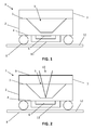
FIG. 1 shows a first device according to embodiments of the present invention. -
FIG. 2 shows a second device according to embodiments of the present invention. -
FIG. 3 illustrates a flow chart of a method according to embodiments of the present invention for manufacturing an integrated infrared sensor device. - The drawings are only schematic and are non-limiting. In the drawings, the size of some of the elements may be exaggerated and not drawn on scale for illustrative purposes.
- Any reference signs in the claims shall not be construed as limiting the scope.
- In the different drawings, the same reference signs refer to the same or analogous elements.
- The present invention will be described with respect to particular embodiments and with reference to certain drawings but the invention is not limited thereto but only by the claims. The drawings described are only schematic and are non-limiting. In the drawings, the size of some of the elements may be exaggerated and not drawn on scale for illustrative purposes. The dimensions and the relative dimensions do not correspond to actual reductions to practice of the invention.
- Furthermore, the terms first, second and the like in the description and in the claims, are used for distinguishing between similar elements and not necessarily for describing a sequence, either temporally, spatially, in ranking or in any other manner. It is to be understood that the terms so used are interchangeable under appropriate circumstances and that the embodiments of the invention described herein are capable of operation in other sequences than described or illustrated herein.
- Moreover, the terms top, under and the like in the description and the claims are used for descriptive purposes and not necessarily for describing relative positions. It is to be understood that the terms so used are interchangeable under appropriate circumstances and that the embodiments of the invention described herein are capable of operation in other orientations than described or illustrated herein.
- It is to be noticed that the term "comprising", used in the claims, should not be interpreted as being restricted to the means listed thereafter; it does not exclude other elements or steps. It is thus to be interpreted as specifying the presence of the stated features, integers, steps or components as referred to, but does not preclude the presence or addition of one or more other features, integers, steps or components, or groups thereof. Thus, the scope of the expression "a device comprising means A and B" should not be limited to devices consisting only of components A and B. It means that with respect to the present invention, the only relevant components of the device are A and B.
- Reference throughout this specification to "one embodiment" or "an embodiment" means that a particular feature, structure or characteristic described in connection with the embodiment is included in at least one embodiment of the present invention. Thus, appearances of the phrases "in one embodiment" or "in an embodiment" in various places throughout this specification are not necessarily all referring to the same embodiment, but may. Furthermore, the particular features, structures or characteristics may be combined in any suitable manner, as would be apparent to one of ordinary skill in the art from this disclosure, in one or more embodiments.
- Similarly it should be appreciated that in the description of exemplary embodiments of the invention, various features of the invention are sometimes grouped together in a single embodiment, figure, or description thereof for the purpose of streamlining the disclosure and aiding in the understanding of one or more of the various inventive aspects. This method of disclosure, however, is not to be interpreted as reflecting an intention that the claimed invention requires more features than are expressly recited in each claim. Rather, as the following claims reflect, inventive aspects lie in less than all features of a single foregoing disclosed embodiment. Thus, the claims following the detailed description are hereby expressly incorporated into this detailed description, with each claim standing on its own as a separate embodiment of this invention.
- Furthermore, while some embodiments described herein include some but not other features included in other embodiments, combinations of features of different embodiments are meant to be within the scope of the invention, and form different embodiments, as would be understood by those in the art. For example, in the following claims, any of the claimed embodiments can be used in any combination.
- In the description provided herein, numerous specific details are set forth. However, it is understood that embodiments of the invention may be practiced without these specific details. In other instances, well-known methods, structures and techniques have not been shown in detail in order not to obscure an understanding of this description.
- In a first aspect, the present invention relates to an integrated infrared sensor device. This device comprises a first substrate, further referred to as the sensor substrate. This sensor substrate has a first surface, further referred to as the back surface, and a second surface, further referred to as the front surface, the front surface being on a side of the substrate opposite to the side of the back surface. Furthermore, the front surface may refer to the side of the substrate on which integrated circuitry is provided in standard integrated circuit manufacturing process steps, while the back surface may refer to the side of the substrate which corresponds to the bulk material, e.g. the side which typically will not have circuitry features processed thereon or which has fewer and/or larger scale processed features thereon when compared to the front surface.
- In a device according to the first aspect of the invention, a cavity is defined in the back surface, while the front surface has at least one infrared sensing element formed therein or arranged thereon, e.g. at least one infrared sensing element is arranged in or on the front surface. Over the at least one sensing element, at the front surface, a cap is provided for protecting the at least one sensing element, e.g. against mechanical damage and dust, and/or against stray radiation.
- Furthermore, the device comprises a second substrate arranged on the first surface (back surface) of the first substrate, such that the second substrate, further referred to as the filter substrate, at least partially covers the cavity, for example such that the filter substrate substantially covers the cavity, e.g. such that the filter substrate entirely covers the cavity. The filter substrate is furthermore adapted, e.g. adapted in shape and/or composition, to transmit infrared radiation while attenuating radiation outside the infrared spectrum, e.g. attenuating radiation in at least a portion of the visible light spectrum.
- Referring to
FIG. 1 , an integratedinfrared sensor device 1 according to embodiments of the present invention is shown. This integratedinfrared sensor device 1 may be an infrared sensor module, e.g. a semiconductor module comprising an infrared sensing element, e.g. a complementary metal-oxide semiconductor (CMOS) infrared sensor module embedded in a chip-scale package. For example, the integratedinfrared sensor device 1 may be adapted in shape and physical dimensions such that the package footprint area is equal to or less than 1.2 times the area of the semiconductor die in or on which the infrared sensing element is implemented, e.g. such integrated circuit chip carrier may be a wafer-level chip-scale package or a wafer-level package. - It is an advantage of an integrated
infrared sensor device 1 according to embodiments of the present invention that the sensor device can be easily manufactured, e.g. using wafer level processing. Furthermore, it is an advantage that such integratedinfrared sensor device 1 can have a small volume, and particularly, a low height profile. - The integrated
infrared sensor device 1 comprises asensor substrate 2, e.g. a first wafer. Thissensor substrate 2 may comprise a semiconductor material, such as silicon or germanium. Thesensor substrate 2 may be a semiconductor substrate suitable for being processed by complementary metal-oxide semiconductor (CMOS) manufacturing steps, e.g. the sensor substrate may be a p-type semiconductor substrate suitable for CMOS processing. - The
sensor substrate 2 comprises aback surface 3 and afront surface 4 opposite theback surface 3, e.g. thesensor substrate 2 may be a planar semiconductor substrate having two sides, corresponding to theback surface 3 and thefront surface 4. In theback surface 3, acavity 5 is defined. For example, a cavity may be provided in theback surface 3 by etching away a portion of the sensor substrate. For example, an anisotropic etching, e.g. an orientation dependent wet etching, may be applied to theback surface 3 to define thecavity 5 therein. In embodiments of the present invention, thecavity 5 may be provided by applying a potassium hydroxide (KOH) wet etching to the back surface. It is particularly advantageous to provide such cavity by applying a back surface etch, as this allows etching the cavity without damaging circuitry, interconnections and/or components already manufactured in or on the front surface. - At least one
infrared sensing element 6 is arranged on thefront surface 4 or formed in thefront surface 4. For example, the at least oneinfrared sensing element 6 may comprise a first and a second temperature-sensitive element in a dielectric stack, for example such that at least one thermocouple is formed, e.g. such that a thermopile is formed. Thecavity 5 may furthermore be adapted for thermally insulating the first temperature-sensitive element from the second temperature-sensitive element. - For example, the integrated infrared sensor device may comprise a volume of infrared absorbing material, e.g. arranged in or on the
front surface 4, and exposed to incident infrared radiation, e.g. radiation transmitted through thefilter substrate 7 and thecavity 5. A temperature difference between this absorber and the surrounding material, e.g. the bulk semiconductor material of thesensor substrate 2, can then be registered to quantify the amount of incident radiation, e.g. a voltage, current, resistance or other electrical quantity which is influenced by the temperature difference can be recorded. The temperature difference may for example be detected by one or more thermocouples having hot junctions in or near the absorber and cold junctions in or near the surrounding material. - Thermal isolation between the absorber and the surrounding material may be provided by the
cavity 5. The semiconductor material between thecavity 5 and the absorbing material is thus thinned out such that thermal contact of the absorber with the sensor wafer material is reduced. - For example, an integrated circuit may be provided in and/or on the
front surface 4. Such integrated circuit may thus implement one or moreinfrared sensing element 6, but may also comprise additional integrated circuit elements for, for example, applying amplification, analog-to-digital conversion, serialization, filtering or other processing to the output produced by the at least oneinfrared sensing element 6. The integrated circuit may also comprise a thermistor element for registering a reference temperature of a bulk portion of the first substrate, e.g. a portion which implements a heat sink thermally connected to at least one cold junction of the at least oneinfrared sensing element 6. Such integrated circuit may comprise processing means, e.g. an ASIC, implemented on the same semiconductor die as theinfrared sensing element 6, such that no wiring is required for operably connecting the infrared sensing element to the ASIC. - The infrared sensor device also comprises a
cap 11, arranged on thefront surface 4, e.g. covering the one or moreinfrared sensing elements 6. Thecap 11 may be made of semiconductor material, for instance silicon or germanium. Cap dimensions should be suitable for covering the one or moreinfrared sensing elements 6. Cap size may for instance between 2 mm x 2 mm and 3 mm x 3 mm, and between 0.3 mm to 1.0 mm thick. The cap cavity can be made by any suitable method from a piece of semiconductor material, for instance by means of cheap wet etch techniques. It is an advantage of acap 11 according to embodiments of the present invention that it can cheaply - in view of its small size - incorporate an optical filter to do wavelength selective detection for, for instance, gas detection. External optical filters have to be much bigger in view of the optics present, and are thus much more expensive. - The
cap 11 may protect the sensor, for instance a sensor membrane, against mechanical damage and dust. Thecap 11 furthermore may protect the sensor from the effect of visible light which would make temperature measurements impossible. - In embodiments of the present invention, the cap can integrate diffractive or refractive lens optics.
- A cavity may be made in the
cap 11, such that space is present between thesensor 6 and thecap 11. That cavity can be made vacuum, which improves the sensitivity of thesensor 6. - Furthermore, the
device 1 comprises asecond substrate 7, the filter substrate, arranged on thefirst surface 3 of thesensor substrate 2, such that thefilter substrate 7 at least partially covers thecavity 5, for example such that thefilter substrate 7 substantially covers thecavity 5, e.g. such that thefilter substrate 7 entirely covers thecavity 5. Thefilter substrate 7 is furthermore adapted in shape and composition to transmit infrared radiation incident thereon. Thefilter substrate 7 may advantageously be adapted for reflecting or strongly attenuating radiation outside the infrared spectrum, for example at least part of the visible spectrum. - In a device according to embodiments of the present invention, the
filter substrate 7 may be bonded to theback surface 3 of thesensor substrate 2, for example using an adhesive, such that a closure of thecavity 5 is obtained that sufficiently shuts out stray light outside the infrared spectrum, e.g. visible light which might interfere with the operation of theinfrared sensing element 6. For example, thefilter substrate 7 may be bonded to theback surface 3 of thesensor substrate 2 by glass frit bonding. - In embodiments of the present invention, the integrated
infrared sensor device 1 may also comprise at least onesolder bump 8 arranged on thefront surface 4 of thesensor substrate 2 for connecting the integrated infrared sensor device to acarrier 12 in a flip-chip arrangement. Such at least onesolder bump 8 may advantageously thermally connect the integratedinfrared sensor device 1 to thecarrier 12, e.g. may provide an efficient thermally conductive path between thecarrier 12 and the bulk material of thesensor substrate 2, e.g. such that one leg of a thermopile can be maintained at substantially the local background temperature. Furthermore, the at least onesolder bump 8 may alternatively or additionally provide an electrically conductive path, for example for enabling an output electrical signal indicative of the amount of incident infrared radiation to be transmitted from the infrared sensor device to thecarrier 12, e.g. to a printed circuit board having supporting electronics provided thereon for further manipulating such electrical signal. - Here, the flip chip arrangement refers to a controlled collapse chip connection mechanism as known in the art, where an integrated circuit semiconductor device, such as the integrated
infrared sensor device 1 according to embodiments, is connected to external circuitry withsolder bumps 8 that may have been deposited onto chip pads. These solder bumps 8 may be deposited on the chip pads on the top side of the wafer during the final wafer processing step. In order to mount the chip to external circuitry, e.g. to a circuit board or another chip or wafer, it is flipped over so that its top side faces down, and aligned so that its pads align with matching pads on the external circuit. Then, the interconnection can be completed by melting the solder. Furthermore, such close contact interconnect achieved by a flip chip arrangement may have the advantage of blocking out stray light, e.g. infrared and/or visible light, from thefront surface 4, which might otherwise interfere with the operation of the at least oneinfrared sensing element 6. - The
device 1 according to embodiments of the present invention may also comprise alternative means for providing a flip-chip arrangement, e.g. instead of or in addition to the at least onesolder bump 8, gold balls or moulded studs or protrusions composed of an electrically conductive polymer may be used. For example, a plated bump process may be used. - Referring to
FIG. 2 , a second device according to embodiments of the invention is shown. Same or similar elements as inFIG. 1 are not described in detail again, but are indicated with same reference numbers. Here, the integratedinfrared sensor device 1 furthermore comprises acoating 9 applied to thefilter substrate 7 for collimating the field ofview 10 of the at least oneinfrared sensing element 6. For example, a peripheral region with respect to the at least oneinfrared sensing element 6 underneath may be provided with acoating 9 to substantially block incident radiation, e.g. to reflect or attenuate infrared radiation incident thereon, while a more central region with respect to theinfrared sensing element 6 underneath is not provided with such coating, e.g. such that infrared radiation incident on this central region may propagate through thefilter substrate 7 in a substantially unattenuated manner. - In a second aspect, the present invention relates to a method for manufacturing an integrated infrared sensor device, e.g. an integrated infrared sensor device according to embodiments of the first aspect of the present invention.
- Referring to
FIG. 3 anexemplary method 30 for manufacturing an integrated infrared sensor device according to this second aspect of the invention is shown. Thismethod 30 comprises the step of obtaining 31 asensor substrate 2 having aback surface 3 and afront surface 4 opposite theback surface 3. Thesensor substrate 2 may for example be a semiconductor substrate suitable for CMOS processing, e.g. a p-type or n-type silicon substrate. - The
method 30 further comprises providing 33 at least oneinfrared sensing element 6 on thefront surface 4 of thesensor substrate 2. For example, integrated circuits may be created on the sensor substrate wafer using process steps as known in the art. The integrated circuits may implement the at least oneinfrared sensing element 6, but also other components, e.g. an ASIC for converting the signal provided by theinfrared sensing element 6 to an output signal of the sensor device. Process steps for creating such integrated circuits may for example comprise standard CMOS processing techniques. - After having provided 33 the at least one
infrared sensing element 6, a method according to embodiments of the present invention provides a step of providing 37 acap 11 over the at least onesensing element 6. Thecap 11 is provided for protecting the at least one sensing element, e.g. against mechanical damage and dust, and/or against stray radiation. - The
method 30 also comprises etching 32 acavity 5 in theback surface 3 of thesensor substrate 2, for example, etching away the substrate material around a position on theback surface 3 corresponding, e.g. orthogonally opposite, to a position of the at least oneinfrared sensing element 6 on thefront surface 4. Themethod 30 may thus comprise etching 32 acavity 5 in theback surface 3 to restrict thermal conduction from the at least oneinfrared sensing element 6 to the bulk material of the sensor substrate. - The
method 30 further comprises providing 34 afilter substrate 7 on theback surface 3 of thesensor substrate 2 for at least partially covering thecavity 5, e.g. for completely covering thecavity 5. Thisfilter substrate 7 is adapted in shape and composition to transmit infrared radiation and to attenuate radiation in at least part of the visible light spectrum, as explained in detail in relation to the first aspect of the invention. - The
method 30 may furthermore comprise the step of metallizing 35 at least one portion of thefront surface 4 to form at least one contact pad, and depositing at least onesolder bump 8 on the at least one contact pad. For example, themethod 30 may comprise metallizing portions of thefront surface 4 to form contact pads, and depositing asolder dot 8 on each of these contact pads. - Furthermore, the
method 30 may comprise re-melting the at least onesolder bump 8 while thefront surface 4 is positioned on acarrier 12 such that the at least onesolder bump 8 is aligned with an at least one corresponding connector on thecarrier 12. Thus, themethod 30 may optionally also comprise re-melting thesolder dots 8, e.g. using hot air reflow, while the front surface is positioned on acarrier 12 such that thesolder dots 8 are facing corresponding connectors on thecarrier 12, e.g. for connecting to external circuitry. For example, to attach the device in flip-chip arrangement onto a circuit, the solder dots may be brought down onto connectors on the underlying electronics or circuit board. The solder may then be re-melted to produce an electrical connection, e.g. using an ultrasonic or alternatively reflow solder process. Thus, only a small space can separate the device's circuitry from the underlying mounting. An electrically-insulating adhesive may furthermore be underfilled to provide a stronger mechanical connection, to provide a heat bridge, and to ensure the solder joints are not stressed due to differential heating of the chip and the rest of the system. It is an advantage of such an assembly that it may be smaller than a traditional carrier-based system and that the chip sits directly on the circuit board, e.g. such that light interfering with infrared radiation detection is blocked out from the carrier side. Also, the short connection path length may reduce inductance, thus allowing high speed signals, and good heat conduction.
Claims (9)
- An integrated infrared sensor device (1), comprising:- a sensor substrate (2) having a back surface (3) and a front surface (4) opposite the back surface (3), said back surface (3) having a cavity (5) defined therein, said front surface (4) having at least one infrared sensing element (6) formed therein or arranged thereon, and- a filter substrate (7) arranged on said back surface (3) of the sensor substrate (2) such that said filter substrate (7) at least partially covers the cavity (5), the filter substrate (7) furthermore being adapted in shape and composition to transmit infrared radiation and to attenuate radiation in at least part of the visible light spectrum, and- a cap (11) for protecting the at least one sensing element (6), said cap (11) being arranged on the front surface (4).
- The integrated infrared sensor device (1) according to claim 1, furthermore comprising at least one solder bump (8) arranged on the front surface (4) of the sensor substrate (2) for connecting the integrated infrared sensor device (1) to a carrier (12) in a flip-chip arrangement.
- The integrated infrared sensor device (1) according to any of the previous claims, in which said filter substrate (7) is bonded to the back surface (3) of the sensor substrate (2).
- The integrated infrared sensor device (1) according to claim 3, in which said filter substrate (7) is bonded to said back surface (3) by glass frit bonding.
- The integrated infrared sensor device (1) according to any of the previous claims, in which said at least one infrared sensing element (6) comprises a first and a second temperature-sensitive element in a dielectric stack, said cavity (5) being adapted for thermally insulating said first temperature-sensitive element from said second temperature-sensitive element.
- The integrated infrared sensor device (1) according to any of the previous claims, furthermore comprising a coating (9) applied to said filter substrate (7) for collimating a field of view (10) of said at least one infrared sensing element (6).
- A method (30) for manufacturing an integrated infrared sensor device (1), the method (30) comprising :- obtaining (31) a sensor substrate (2) having a back surface (3) and a front surface (4) opposite the back surface (3),- providing (33) at least one infrared sensing element (6) on said front surface (4),- providing (37) a cap over the at least one sensing element (6) for protecting the at least one sensing element (6),- etching (32) a cavity (5) in said back surface (3), and- providing (34) a filter substrate (7) on said back surface (3) for at least partially covering the cavity (5), in which said filter substrate (7) is adapted in shape and composition to transmit infrared radiation and to attenuate radiation in at least part of the visible light spectrum.
- The method (30) according to claim 7, furthermore comprising the step of metallizing (35) at least one portion of the front surface (4) to form at least one contact pad, and depositing at least one solder bump (8) on the at least one contact pad.
- The method (30) according to claim 8, further comprising remelting the at least one solder bump (8) while the front surface (4) is positioned on a carrier (12) such that the at least one solder bump (8) is aligned with an at least one corresponding connector on the carrier.
Applications Claiming Priority (1)
| Application Number | Priority Date | Filing Date | Title |
|---|---|---|---|
| GB1407477.7A GB2525612A (en) | 2014-04-29 | 2014-04-29 | Infrared sensor package |
Publications (1)
| Publication Number | Publication Date |
|---|---|
| EP2940442A1 true EP2940442A1 (en) | 2015-11-04 |
Family
ID=50972011
Family Applications (1)
| Application Number | Title | Priority Date | Filing Date |
|---|---|---|---|
| EP15165772.3A Withdrawn EP2940442A1 (en) | 2014-04-29 | 2015-04-29 | Infrared sensor package |
Country Status (3)
| Country | Link |
|---|---|
| US (1) | US9534959B2 (en) |
| EP (1) | EP2940442A1 (en) |
| GB (1) | GB2525612A (en) |
Cited By (2)
| Publication number | Priority date | Publication date | Assignee | Title |
|---|---|---|---|---|
| WO2018122148A1 (en) | 2016-12-30 | 2018-07-05 | Heimann Sensor Gmbh | Smd-enabled infrared thermopile sensor |
| WO2026077531A1 (en) * | 2024-10-09 | 2026-04-16 | Melexis Technologies Nv | Thermal sensor module and method of manufacture thereof |
Families Citing this family (3)
| Publication number | Priority date | Publication date | Assignee | Title |
|---|---|---|---|---|
| US10371578B2 (en) * | 2015-04-14 | 2019-08-06 | Maxim Integrated Products, Inc. | Thermal management of thermal sensor in a mobile device |
| TWI672820B (en) * | 2018-02-06 | 2019-09-21 | Luxnet Corporation | Optical receiver and manufaturing method thereof |
| KR102926962B1 (en) * | 2021-06-29 | 2026-02-11 | 삼성전자주식회사 | Sensor for sensing heat or infrared light and electronic device including same |
Citations (10)
| Publication number | Priority date | Publication date | Assignee | Title |
|---|---|---|---|---|
| JPH11258041A (en) * | 1998-03-12 | 1999-09-24 | Omron Corp | Thermopile type infrared sensor |
| US5962854A (en) * | 1996-06-12 | 1999-10-05 | Ishizuka Electronics Corporation | Infrared sensor and infrared detector |
| JP2000298063A (en) * | 1999-04-14 | 2000-10-24 | Tdk Corp | Infrared ray detector |
| JP2004037297A (en) * | 2002-07-04 | 2004-02-05 | Denso Corp | Infrared sensor and manufacturing method thereof |
| US6828560B2 (en) * | 2002-01-31 | 2004-12-07 | Delphi Technologies, Inc. | Integrated light concentrator |
| US20050081905A1 (en) * | 2003-10-17 | 2005-04-21 | Lan Alex H. | Thermopile IR detector package structure |
| US20060038129A1 (en) * | 2004-08-04 | 2006-02-23 | Denso Corporation | Infrared sensor device and its manufacturing method |
| US20070063145A1 (en) * | 2005-09-21 | 2007-03-22 | Oliver Kierse | Radiation sensor device and method |
| US20080202209A1 (en) * | 2005-01-26 | 2008-08-28 | Analog Devices, Inc. | Sensor |
| US20100213374A1 (en) * | 2009-02-26 | 2010-08-26 | Texas Instruments Incorporated | On-chip calibration system and method for infrared sensor |
Family Cites Families (6)
| Publication number | Priority date | Publication date | Assignee | Title |
|---|---|---|---|---|
| KR100477784B1 (en) * | 2000-08-31 | 2005-03-22 | 매그나칩 반도체 유한회사 | Image sensor having lens formed by air in trench and method for fabricating the same |
| US7180064B2 (en) * | 2003-07-24 | 2007-02-20 | Delphi Technologies, Inc. | Infrared sensor package |
| US8304850B2 (en) | 2009-12-22 | 2012-11-06 | Texas Instruments Incorporated | Integrated infrared sensors with optical elements, and methods |
| TWI369483B (en) * | 2010-08-30 | 2012-08-01 | Unimems Mfg Co Ltd | Miniature infrared sensor and manufacturing method thereof |
| JP2014241376A (en) * | 2013-06-12 | 2014-12-25 | 住友電気工業株式会社 | Image sensor |
| US9113096B1 (en) * | 2014-06-30 | 2015-08-18 | Amazon Technologies, Inc. | Single sensor two-sided camera |
-
2014
- 2014-04-29 GB GB1407477.7A patent/GB2525612A/en not_active Withdrawn
-
2015
- 2015-04-29 US US14/699,112 patent/US9534959B2/en active Active
- 2015-04-29 EP EP15165772.3A patent/EP2940442A1/en not_active Withdrawn
Patent Citations (10)
| Publication number | Priority date | Publication date | Assignee | Title |
|---|---|---|---|---|
| US5962854A (en) * | 1996-06-12 | 1999-10-05 | Ishizuka Electronics Corporation | Infrared sensor and infrared detector |
| JPH11258041A (en) * | 1998-03-12 | 1999-09-24 | Omron Corp | Thermopile type infrared sensor |
| JP2000298063A (en) * | 1999-04-14 | 2000-10-24 | Tdk Corp | Infrared ray detector |
| US6828560B2 (en) * | 2002-01-31 | 2004-12-07 | Delphi Technologies, Inc. | Integrated light concentrator |
| JP2004037297A (en) * | 2002-07-04 | 2004-02-05 | Denso Corp | Infrared sensor and manufacturing method thereof |
| US20050081905A1 (en) * | 2003-10-17 | 2005-04-21 | Lan Alex H. | Thermopile IR detector package structure |
| US20060038129A1 (en) * | 2004-08-04 | 2006-02-23 | Denso Corporation | Infrared sensor device and its manufacturing method |
| US20080202209A1 (en) * | 2005-01-26 | 2008-08-28 | Analog Devices, Inc. | Sensor |
| US20070063145A1 (en) * | 2005-09-21 | 2007-03-22 | Oliver Kierse | Radiation sensor device and method |
| US20100213374A1 (en) * | 2009-02-26 | 2010-08-26 | Texas Instruments Incorporated | On-chip calibration system and method for infrared sensor |
Cited By (5)
| Publication number | Priority date | Publication date | Assignee | Title |
|---|---|---|---|---|
| WO2018122148A1 (en) | 2016-12-30 | 2018-07-05 | Heimann Sensor Gmbh | Smd-enabled infrared thermopile sensor |
| DE102017131049A1 (en) | 2016-12-30 | 2018-07-05 | Heimann Sensor Gmbh | SMD-compatible Thermopile infrared sensor |
| US11268861B2 (en) | 2016-12-30 | 2022-03-08 | Heimann Sensor Gmbh | SMD-enabled infrared thermopile sensor |
| EP4191215A1 (en) | 2016-12-30 | 2023-06-07 | Heimann Sensor GmbH | Smd-enabled infrared thermopile sensor |
| WO2026077531A1 (en) * | 2024-10-09 | 2026-04-16 | Melexis Technologies Nv | Thermal sensor module and method of manufacture thereof |
Also Published As
| Publication number | Publication date |
|---|---|
| US9534959B2 (en) | 2017-01-03 |
| GB2525612A (en) | 2015-11-04 |
| GB201407477D0 (en) | 2014-06-11 |
| US20150308899A1 (en) | 2015-10-29 |
Similar Documents
| Publication | Publication Date | Title |
|---|---|---|
| US8519336B2 (en) | Infrared sensor and infrared sensor module | |
| CN102884627B (en) | Uncooled ir detector and the method for the manufacture of uncooled ir detector | |
| JP2021009152A (en) | Thermal infrared sensor array in wafer level package | |
| US10439118B2 (en) | MEMS-based wafer level packaging for thermo-electric IR detectors | |
| KR102609052B1 (en) | Surface micro-machined infrared sensor using highly temperature stable interferometric absorber | |
| US9534959B2 (en) | Infrared sensor package | |
| KR102715529B1 (en) | Infrared device | |
| US11953380B2 (en) | Combined near and mid infrared sensor in a chip scale package | |
| KR102826379B1 (en) | Method for producing a thermal infrared sensor array within a vacuum-filled wafer level housing | |
| JP2000298063A (en) | Infrared ray detector | |
| KR101588642B1 (en) | Method for manufacturing wafer Level Packaging Device | |
| KR20160122872A (en) | Wafer level packaging device | |
| US10644047B2 (en) | Optoelectronic device with a refractive element and a method of producing such an optoelectronic device | |
| US9035413B2 (en) | Semiconductor device with embedded converter element and production method for a semiconductor device with an embedded converter element | |
| US20160049434A1 (en) | Digital radiation sensor package | |
| JP2012230010A (en) | Infrared sensor | |
| KR20150132611A (en) | Wafer level packaging device for controlling field of view | |
| JP2012037394A (en) | Method for manufacturing infrared sensor | |
| JP2011203221A (en) | Infrared sensor module | |
| JP2012013516A (en) | Infrared sensor device | |
| JP2011252724A (en) | Infrared sensor and manufacturing method thereof |
Legal Events
| Date | Code | Title | Description |
|---|---|---|---|
| PUAI | Public reference made under article 153(3) epc to a published international application that has entered the european phase |
Free format text: ORIGINAL CODE: 0009012 |
|
| AK | Designated contracting states |
Kind code of ref document: A1 Designated state(s): AL AT BE BG CH CY CZ DE DK EE ES FI FR GB GR HR HU IE IS IT LI LT LU LV MC MK MT NL NO PL PT RO RS SE SI SK SM TR |
|
| AX | Request for extension of the european patent |
Extension state: BA ME |
|
| 17P | Request for examination filed |
Effective date: 20160503 |
|
| RBV | Designated contracting states (corrected) |
Designated state(s): AL AT BE BG CH CY CZ DE DK EE ES FI FR GB GR HR HU IE IS IT LI LT LU LV MC MK MT NL NO PL PT RO RS SE SI SK SM TR |
|
| STAA | Information on the status of an ep patent application or granted ep patent |
Free format text: STATUS: EXAMINATION IS IN PROGRESS |
|
| 17Q | First examination report despatched |
Effective date: 20180615 |
|
| STAA | Information on the status of an ep patent application or granted ep patent |
Free format text: STATUS: THE APPLICATION IS DEEMED TO BE WITHDRAWN |
|
| 18D | Application deemed to be withdrawn |
Effective date: 20190521 |