EP2937940A1 - Connector and contact - Google Patents
Connector and contact Download PDFInfo
- Publication number
- EP2937940A1 EP2937940A1 EP15163956.4A EP15163956A EP2937940A1 EP 2937940 A1 EP2937940 A1 EP 2937940A1 EP 15163956 A EP15163956 A EP 15163956A EP 2937940 A1 EP2937940 A1 EP 2937940A1
- Authority
- EP
- European Patent Office
- Prior art keywords
- connector
- board
- ground
- extension parts
- insulating layer
- Prior art date
- Legal status (The legal status is an assumption and is not a legal conclusion. Google has not performed a legal analysis and makes no representation as to the accuracy of the status listed.)
- Withdrawn
Links
Images






Classifications
-
- H—ELECTRICITY
- H01—ELECTRIC ELEMENTS
- H01R—ELECTRICALLY-CONDUCTIVE CONNECTIONS; STRUCTURAL ASSOCIATIONS OF A PLURALITY OF MUTUALLY-INSULATED ELECTRICAL CONNECTING ELEMENTS; COUPLING DEVICES; CURRENT COLLECTORS
- H01R12/00—Structural associations of a plurality of mutually-insulated electrical connecting elements, specially adapted for printed circuits, e.g. printed circuit boards [PCB], flat or ribbon cables, or like generally planar structures, e.g. terminal strips, terminal blocks; Coupling devices specially adapted for printed circuits, flat or ribbon cables, or like generally planar structures; Terminals specially adapted for contact with, or insertion into, printed circuits, flat or ribbon cables, or like generally planar structures
- H01R12/70—Coupling devices
- H01R12/77—Coupling devices for flexible printed circuits, flat or ribbon cables or like structures
- H01R12/79—Coupling devices for flexible printed circuits, flat or ribbon cables or like structures connecting to rigid printed circuits or like structures
-
- H—ELECTRICITY
- H01—ELECTRIC ELEMENTS
- H01R—ELECTRICALLY-CONDUCTIVE CONNECTIONS; STRUCTURAL ASSOCIATIONS OF A PLURALITY OF MUTUALLY-INSULATED ELECTRICAL CONNECTING ELEMENTS; COUPLING DEVICES; CURRENT COLLECTORS
- H01R12/00—Structural associations of a plurality of mutually-insulated electrical connecting elements, specially adapted for printed circuits, e.g. printed circuit boards [PCB], flat or ribbon cables, or like generally planar structures, e.g. terminal strips, terminal blocks; Coupling devices specially adapted for printed circuits, flat or ribbon cables, or like generally planar structures; Terminals specially adapted for contact with, or insertion into, printed circuits, flat or ribbon cables, or like generally planar structures
- H01R12/50—Fixed connections
- H01R12/51—Fixed connections for rigid printed circuits or like structures
- H01R12/52—Fixed connections for rigid printed circuits or like structures connecting to other rigid printed circuits or like structures
-
- H—ELECTRICITY
- H01—ELECTRIC ELEMENTS
- H01R—ELECTRICALLY-CONDUCTIVE CONNECTIONS; STRUCTURAL ASSOCIATIONS OF A PLURALITY OF MUTUALLY-INSULATED ELECTRICAL CONNECTING ELEMENTS; COUPLING DEVICES; CURRENT COLLECTORS
- H01R12/00—Structural associations of a plurality of mutually-insulated electrical connecting elements, specially adapted for printed circuits, e.g. printed circuit boards [PCB], flat or ribbon cables, or like generally planar structures, e.g. terminal strips, terminal blocks; Coupling devices specially adapted for printed circuits, flat or ribbon cables, or like generally planar structures; Terminals specially adapted for contact with, or insertion into, printed circuits, flat or ribbon cables, or like generally planar structures
- H01R12/70—Coupling devices
- H01R12/77—Coupling devices for flexible printed circuits, flat or ribbon cables or like structures
- H01R12/771—Details
- H01R12/775—Ground or shield arrangements
-
- H—ELECTRICITY
- H01—ELECTRIC ELEMENTS
- H01R—ELECTRICALLY-CONDUCTIVE CONNECTIONS; STRUCTURAL ASSOCIATIONS OF A PLURALITY OF MUTUALLY-INSULATED ELECTRICAL CONNECTING ELEMENTS; COUPLING DEVICES; CURRENT COLLECTORS
- H01R13/00—Details of coupling devices of the kinds covered by groups H01R12/70 or H01R24/00 - H01R33/00
- H01R13/02—Contact members
- H01R13/03—Contact members characterised by the material, e.g. plating, or coating materials
- H01R13/035—Plated dielectric material
-
- H—ELECTRICITY
- H01—ELECTRIC ELEMENTS
- H01R—ELECTRICALLY-CONDUCTIVE CONNECTIONS; STRUCTURAL ASSOCIATIONS OF A PLURALITY OF MUTUALLY-INSULATED ELECTRICAL CONNECTING ELEMENTS; COUPLING DEVICES; CURRENT COLLECTORS
- H01R13/00—Details of coupling devices of the kinds covered by groups H01R12/70 or H01R24/00 - H01R33/00
- H01R13/646—Details of coupling devices of the kinds covered by groups H01R12/70 or H01R24/00 - H01R33/00 specially adapted for high-frequency, e.g. structures providing an impedance match or phase match
- H01R13/6473—Impedance matching
-
- H—ELECTRICITY
- H05—ELECTRIC TECHNIQUES NOT OTHERWISE PROVIDED FOR
- H05K—PRINTED CIRCUITS; CASINGS OR CONSTRUCTIONAL DETAILS OF ELECTRIC APPARATUS; MANUFACTURE OF ASSEMBLAGES OF ELECTRICAL COMPONENTS
- H05K1/00—Printed circuits
- H05K1/02—Details
- H05K1/11—Printed elements for providing electric connections to or between printed circuits
- H05K1/117—Pads along the edge of rigid circuit boards, e.g. for pluggable connectors
-
- H—ELECTRICITY
- H05—ELECTRIC TECHNIQUES NOT OTHERWISE PROVIDED FOR
- H05K—PRINTED CIRCUITS; CASINGS OR CONSTRUCTIONAL DETAILS OF ELECTRIC APPARATUS; MANUFACTURE OF ASSEMBLAGES OF ELECTRICAL COMPONENTS
- H05K1/00—Printed circuits
- H05K1/02—Details
- H05K1/14—Structural association of two or more printed circuits
- H05K1/147—Structural association of two or more printed circuits at least one of the printed circuits being bent or folded, e.g. by using a flexible printed circuit
-
- H—ELECTRICITY
- H01—ELECTRIC ELEMENTS
- H01R—ELECTRICALLY-CONDUCTIVE CONNECTIONS; STRUCTURAL ASSOCIATIONS OF A PLURALITY OF MUTUALLY-INSULATED ELECTRICAL CONNECTING ELEMENTS; COUPLING DEVICES; CURRENT COLLECTORS
- H01R13/00—Details of coupling devices of the kinds covered by groups H01R12/70 or H01R24/00 - H01R33/00
- H01R13/648—Protective earth or shield arrangements on coupling devices, e.g. anti-static shielding
- H01R13/658—High frequency shielding arrangements, e.g. against EMI [Electro-Magnetic Interference] or EMP [Electro-Magnetic Pulse]
- H01R13/6581—Shield structure
- H01R13/6585—Shielding material individually surrounding or interposed between mutually spaced contacts
-
- H—ELECTRICITY
- H05—ELECTRIC TECHNIQUES NOT OTHERWISE PROVIDED FOR
- H05K—PRINTED CIRCUITS; CASINGS OR CONSTRUCTIONAL DETAILS OF ELECTRIC APPARATUS; MANUFACTURE OF ASSEMBLAGES OF ELECTRICAL COMPONENTS
- H05K1/00—Printed circuits
- H05K1/02—Details
- H05K1/03—Use of materials for the substrate
- H05K1/05—Insulated conductive substrates, e.g. insulated metal substrate
-
- H—ELECTRICITY
- H05—ELECTRIC TECHNIQUES NOT OTHERWISE PROVIDED FOR
- H05K—PRINTED CIRCUITS; CASINGS OR CONSTRUCTIONAL DETAILS OF ELECTRIC APPARATUS; MANUFACTURE OF ASSEMBLAGES OF ELECTRICAL COMPONENTS
- H05K1/00—Printed circuits
- H05K1/02—Details
- H05K1/03—Use of materials for the substrate
- H05K1/05—Insulated conductive substrates, e.g. insulated metal substrate
- H05K1/056—Insulated conductive substrates, e.g. insulated metal substrate the metal substrate being covered by an organic insulating layer
-
- H—ELECTRICITY
- H05—ELECTRIC TECHNIQUES NOT OTHERWISE PROVIDED FOR
- H05K—PRINTED CIRCUITS; CASINGS OR CONSTRUCTIONAL DETAILS OF ELECTRIC APPARATUS; MANUFACTURE OF ASSEMBLAGES OF ELECTRICAL COMPONENTS
- H05K2201/00—Indexing scheme relating to printed circuits covered by H05K1/00
- H05K2201/09—Shape and layout
- H05K2201/09145—Edge details
- H05K2201/09172—Notches between edge pads
-
- H—ELECTRICITY
- H05—ELECTRIC TECHNIQUES NOT OTHERWISE PROVIDED FOR
- H05K—PRINTED CIRCUITS; CASINGS OR CONSTRUCTIONAL DETAILS OF ELECTRIC APPARATUS; MANUFACTURE OF ASSEMBLAGES OF ELECTRICAL COMPONENTS
- H05K2201/00—Indexing scheme relating to printed circuits covered by H05K1/00
- H05K2201/09—Shape and layout
- H05K2201/09209—Shape and layout details of conductors
- H05K2201/09218—Conductive traces
- H05K2201/09236—Parallel layout
Definitions
- An aspect of this disclosure relates to a connector and a contact.
- Japanese Laid-Open Patent Publication No. 2003-142183 discloses a contact module that includes a sheet made of a metal, an insulating film formed on at least one surface of the sheet, and a contact formed as a thin film of a noble metal on the insulating film and including contact points and a circuit pattern.
- the impedance of the sheet made of a metal is not matched sufficiently with the impedance of the contact formed on the insulating film on the sheet. Therefore, with the disclosed contact module, it may be difficult to transmit a signal in an impedance matched condition.
- a connector to be connected to a signal wire and a ground wire formed on a board.
- the connector includes a base made of a conductive material, at least two first extension parts that extend from the base toward a first end of the connector, and at least two second extension parts that extend from the base toward a second end of the connector; an insulating layer formed on a surface of the terminal; a signal line that is formed on the insulating layer, is insulated from the terminal, and extends from an end of a first one of the first extension parts to an end of a first one of the second extension parts, the signal line being connected to the signal wire of the board when the connector is attached to the board; and a ground line that is formed on the insulating layer, is electrically connected to the terminal, and extends from an end of a second one of the first extension parts, which is adjacent to the first one of the first extension parts, to an end of a second one of the second extension parts, which is adjacent to the first one of the second extension parts, the ground
- FIGs. 1A and 1B are drawings illustrating connectors 100A and 100B according to an embodiment. As illustrated by FIG. 1A , the connector 100A is attached to a board 300A, and the connector 100B is attached to a board 300B.
- Each of the boards 300A and 300B includes signal lines and ground lines.
- the characteristic impedance of the signal lines and the ground lines of the boards 300A and 300B is set at a predetermined value (e.g., 50 ⁇ ) to enable high-speed signal transmission at, for example, about 2.0 Gbps.
- the signal lines and the ground lines of the boards 300A and 300B with such a characteristic impedance may be implemented by microstrip lines or coplanar lines.
- the connector 100A is connected to the signal lines and the ground lines of the board 300A, and the connector 100B is connected to the signal lines and the ground lines of the board 300B.
- a flexible printed circuit (FPC) assembly 400 includes connectors 410A and 410B and two FPCs 420. Each of the FPCs 420 includes signal lines and ground lines.
- the characteristic impedance of the signal lines and the ground lines of the FPCs 420 is set at a predetermined value (e.g., 50 ⁇ ) to enable high-speed signal transmission at, for example, about 2.0 Gbps.
- the connector 410A is connected to first ends of the FPCs 420, and the connector 410B is connected to second ends of the FPCs 420.
- the connectors 410A and 410B of the FPC assembly 400 are connected to the corresponding connectors 100A and 100B.
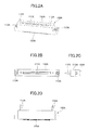
- FIG. 2A is a perspective view
- FIG. 2B is a front view
- FIG. 2C is a side view
- FIG. 2D is a plan view of the connector 100A
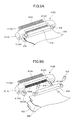
- FIG. 3 is a perspective view of the connector 100A attached to the board 300A.
- the connector 100A includes a housing 110A and contacts 120A.
- the connector 100A is formed by placing the contacts 120A in a through hole 111A of the housing 110A.
- the housing 110A includes guide pins 112A used when the connector 410A is attached to the connector 100A. A bottom of each guide pin 112A is embedded in the body of the housing 110A.
- the housing 110A also includes screw holes 113A.
- Through holes corresponding to the screw holes 113A are formed in the board 300A.
- the screw holes 113 of the housing 110A are aligned with the through holes of the board 300A, and the connector 100A is attached to one surface of the board 300A with screws 500 inserted into the screw holes 113A and the through holes of the board 300A as illustrated by FIG. 1A and FIG. 3 .
- the guide pins 112A may be comprised of a metal such as copper or nickel, or a resin.
- the housing 110A may be comprised of an insulating material such as an epoxy resin.
- the housing 110A may have a cuboid shape, and includes protrusions protruding in the longitudinal direction of the housing 110A.
- the screw holes 113A are formed in the protrusions of the housing 110A.
- Each contact 120A includes a first end and a second end, and extends in a direction that is substantially perpendicular to a surface of the board 300A.
- the second end of the contact 120A to be connected to the board 300A is illustrated in FIGs. 2A, 2C, and 2D , and the first end of the contact 120A is illustrated in FIG. 3 .
- the first end of the contact 120A is connected to the connector 410A of the FPC assembly 400, and the second end of the contact 120A is connected to the signal line and the ground lines of the board 300A.
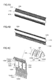
- FIGs. 4A and 4B are perspective views and FIG. 4C is an enlarged view of the contact 120A.
- FIG. 5A is a cross-sectional view taken along line A-A of FIG. 4C
- FIGs. 5B and 5C are enlarged views of parts of FIG. 5A .
- the contact 120A is a linear leaf spring. As illustrated by FIGs. 4A and 4B , twenty-two contacts 120A are bound together with a holder 114A. Each contact 120A includes leaf spring structures that protrude from the holder 114A in opposite directions.
- the holder 114A is a part of the housing 110A (see FIGs. 2A-2D and FIG. 3 ), and is disposed inside of the housing 110A. The internal configuration of the housing 110A is described later with reference to FIG. 7 .
- FIG. 4C illustrates contacts 120A arranged adjacent to each other.
- FIG. 4C also includes an enlarged view of an end portion of one of the contacts 120A.
- the contacts 120A bound together with the holder 114A as illustrated by FIGs. 4A and 4B are arranged as illustrated by FIG. 4C .
- FIG. 4C three of the twenty-two contacts 120A are illustrated as an example, and the holder 114A is omitted.
- Each contact 120A includes a base 121A, extension parts 122A, extension parts 123A, an insulating layer 124, a signal line 125, and two ground lines 126.
- the base 121A, the extension part 122A, and the extension part 123A are formed integrally as a single component that is an example of a ground terminal.
- the base 121A, the extension part 122A, and the extension part 123A may be formed, for example, by punching sheet metal made of, for example, stainless steel and bending the punched sheet metal.
- the insulating layer 124, the signal line 125, and the ground lines 126 are formed on the ground terminal, that is, on the base 121A, the extension part 122A, and the extension part 123A.
- the base 121A is a plate-like part.
- the extension parts 122A and 123A extend from the corresponding ends of the base 121A in the length direction.
- the insulating layer 124 is formed on one surface of the base 121A, and the signal line 125 and the ground lines 126 are formed on the insulating layer 124.
- the extension part 122A extends from one end (the lower end in FIG. 4C ) of the base 121A and branches into three extension parts, one extension part 122A1 in the middle and two extension parts 122A2 provided on the sides of the extension part 122A1.
- the signal line 125 is formed on the insulating layer 124.
- the ground lines 126 are formed on the insulating layer 124. The signal line 125 and the ground lines 126 formed on the extension part 122A are connected to the signal line 125 and the ground lines 126 formed on the base 121A.
- the insulating layer 124, the signal line 125, and the ground lines 126 formed on the back side of the extension part 122A are not visible, their configurations are substantially the same as those of the insulating layer 124, the signal line 125, and the ground lines 125 formed on the extension part 123A.
- the signal line 125 and the ground lines 126 formed on the extension part 122A are to be connected to the connector 410A (see FIGs. 1A and 1B ).
- the extension part 122A has a leaf spring structure.
- the leaf spring structure of the extension part 122A is configured such that an elastic force acts in such a direction that a distance between a pair of opposing extension parts 122A is reduced.
- the extension part 123A extends from another end (the upper end in FIG. 4C ) of the base 121A and branches into three extension parts, an extension part 123A1 in the middle and two extension parts 123A2 on the sides of the extension part 123A1.
- the signal line 125 is formed on the insulating layer 124.
- the ground lines 126 are formed on the insulating layer 124.
- the signal line 125 and the ground lines 126 formed on the extension part 123A are connected to the signal line 125 and the ground lines 126 formed on the extension part 122A via the signal line 125 and the ground lines 126 formed on the base 121A.
- the signal line 125 and the ground lines 126 formed on the extension part 123A are to be connected to the corresponding signal line and ground lines on the board 300A.
- the extension part 123A has a leaf spring structure whose end portion has a curved shape. When the curved end portion is pressed toward the base 121A, the extension part 123A elastically bends and a restoring force is generated. This leaf spring structure enables reliable electrical connection between the end of the extension part 123A and the signal line and the ground lines of the board 300A.
- FIG. 5A illustrates the insulating layer 124, the signal line 125, and the ground lines 126 formed on one surface of the base 121A.
- the insulating layer 124 is formed on the base 121A, the extension part 122A, and the extension part 123A.
- the signal line 125 and the ground lines 126 are formed continuously on the base 121A, the extension part 122A, and the extension part 123A via the insulating layer 124.
- FIG. 5A illustrates a cross section of the base 121A on which the insulating layer 124, the signal line 125, and the ground lines 126 are formed.
- a cross section of each of the extension part 122A and the extension part 123A may be obtained by dividing the cross section of FIG. 5A into three sections in the horizontal direction.
- the insulating layer 124 may be implemented by, for example, a polyimide film.
- the insulating layer 124 is pasted onto the base 121A, the extension part 122A, and the extension part 123A.
- the signal line 125 includes a Cu plated layer 125A, an Ni plated layer 125B, and an Au plated layer 125C.
- the signal line 125 may be formed on the insulating layer 124 by a plating process.
- a groove 124A is formed in a part of the insulating layer 124 below the ground line 126.
- the groove 124A passes through the insulating layer 124 in the thickness direction, and extends from one end to the other end of the ground line 126 in the length direction.
- the ground line 126 includes a Cu plated layer 126A, an Ni plated layer 126B, and an Au plated layer 126C.
- the ground line 126 may be formed on the insulating layer 124 by a plating process.
- the ground line 126 is physically and electrically connected to the base 121A, the extension part 122A, and the extension part 123A that function as a ground terminal. Accordingly, the ground line 126 is kept at a ground potential.
- the groove 124A formed in the insulating layer 124 extends continuously from one end to the other end of the ground line 126.
- the groove 124A may be formed to extend intermittently from one end to the other end of the ground line 126.
- Through holes passing through the insulating layer 124 may be formed at predetermined intervals along the ground line 126 instead of the groove 124A.
- the protective film may be implemented by, for example, a polyimide film.
- the base 121A, the extension part 122A, and the extension part 123A of the contact 120A function as a ground terminal that is kept at a ground potential. Accordingly, the signal line 125, the base 121A, the extension part 122A, and the extension part 123A form a microstrip line.
- the ground lines 126 are formed on the sides of the signal line 125 at the same height as and parallel to the signal line 125. Accordingly, the signal line 125 and the ground lines 126 form a coplanar line.
- the contact 120A is configured as described above to achieve good impedance matching between the board 300A and the connector 410A, to reduce reflection and transmission loss of a signal, and to improve signal transmission characteristics.
- the characteristic impedance of the signal line 125 of the contact 120A can be set at a predetermined value (e.g., 50 ⁇ ).
- FIGs. 6 and 7 illustrate the connector 100A.
- FIG. 7 is a cross-sectional view taken along line B-B of FIG. 6 .
- the holder 114A may be implemented as a resin part that is formed by insert molding to hold the bases 121A of the contacts 120A together.
- the holder 114A may be implemented as a V-shaped part including two arm parts that are joined at one end. The arm parts are placed to sandwich the bases 121A of the contacts 120A, and are then joined at the other end to hold the contacts 120A together.
- the through hole 111A of the housing 110A includes an opening 111A1, a middle portion 111A2, and an opening 111A3.
- the opening 111A1 is formed between the guide pins 112A as indicated by the reference number 111A in FIG. 6 .
- the opening 111A3 is divided into two openings by a partition wall 115A of the housing 110A.
- the holder 114A of one set of the contacts 120A is fitted into the upper opening of the opening 111A3.
- the gap between an inner wall 110A1 of the housing 110A and the partition wall 115A is set at a value that is substantially the same as the thickness of the holder 114A so that the holder 114A can be fitted into the gap.
- the housing 110A also includes two engaging parts 116A at the boundary between the opening 111A1 and the middle portion 111A2.
- the engaging parts 116A are formed to extend along the length direction of the opening 111A1, and to protrude into the middle portion 111A2.
- the extension part 122A With the end of the extension part 122A engaging with the engaging part 116A and the holder 114A holding the base 121A fitted into the gap between the inner wall 110A1 and the partition wall 115, the extension part 122A can function as a leaf spring.
- the other set of the contacts 120A is still outside of the housing 110A.
- the corresponding extension parts 122A of the two sets of the contacts 120A face each other, and the signal lines 125 and the ground lines 126 formed on the corresponding extension parts 122A also face each other.
- the conductive part of the connector 410A is inserted into the connector 100A through the opening 111A1, the extension parts 122A are brought into contact with the conductive part and are elastically bent.
- FIG. 8A is a perspective view
- FIG. 8B is a front view
- FIG. 8C is a side view
- FIG. 8D is a plan view of the connector 410A of the FPC assembly 400 to which the connector 100A is to be connected.
- the connector 410A includes a housing 411A and forty-four contacts 412A.
- the housing 411A includes a base 411A1, a protrusion 411A2, guide pin holes 411A3 for guide pins, holes 411A4 for floating screws, and holes 411A5.
- the base 411A1 is a base of the housing 411A.
- the protruding part 411A2 has a shape like a flat plate and protrudes from the base 411A1.
- the forty-four contacts 412A are arranged on the surfaces of the protruding part 411A2. Twenty two of the forty-four contacts 412A are arranged on one surface of the protruding part 411A2, and the remaining twenty-two contacts 412A are arranged on the other surface of the protruding part 411A2.
- the protruding part 411A2 is provided separately from the base 411A1, and is fitted into a through hole of the base 411A1.
- the connector 410A of FIGs. 8A through 8D is formed by fitting the protruding part 411A2 into the through hole of the base 411A1 after the contacts 412A are attached to the surfaces of the protruding part 411A2.
- Each contact 412A includes one signal line and two ground lines on the sides of the signal line that correspond to the signal line 125 and the ground lines 126 of the contact 120A.
- a first end of the contact 412A extends up to an end of the protruding part 411A2 as illustrated by FIG. 8A , and a second end of the contact 412A extends in a direction opposite from the direction in which the protruding part 411A2 protrudes from the base 411A1 as illustrated by FIG. 8D .
- the first end of the contact 412A is connected to the signal line 125 and the ground lines 126 of the connector 100A, and the second end of the contact 412A is connected to the signal line and the ground lines of one of the FPCs 420.
- the contact 412A of the connector 410A includes a coplanar line.
- the contact 412A is configured as described above to achieve good impedance matching between the connector 100A and the FPCs 420, to reduce reflection and transmission loss of a signal, and to improve signal transmission characteristics.
- the contact 412A of the present embodiment is an SMT (surface mount technology) contact, and may be formed by mounting a patterned metal plate on the protruding part 411A2.
- the guide pin holes 411A3 receive the guide pins 112A of the connector 100A.
- the floating screw holes 411A4 receive screws for fastening the connector 100A and the connector 410A connected together as illustrated in FIG. 1A .
- the holes 411A5 accept parts for fastening the FPCs 420 to the connector 410A.
- the above configuration of the connector 410A also applies to the connector 410B (see FIGs. 1A and 1B ).
- FIGs. 9A and 9B are drawings illustrating a mechanism for attaching the connector 410A to the FPCs 420.
- FIG. 9A is a perspective view
- FIG. 9B is an exploded view of FIG. 9A .
- the two sets of the twenty-two contacts 412A are sandwiched between the two FPCs 420.
- the FPCs 420 are fixed to the housing 411A with a holder 415, and screws 416 are inserted into through holes at the ends of the holder 415 and then into the holes 411A5 of the connector 410A to attach the connector 410A to first ends of the FPCs 420 as illustrated by FIG. 9A .
- the signal lines and the ground lines formed on the two FPCs 420 are connected to the signal lines and the ground lines of the contacts 412A of the connector 410A.
- the connector 410B has substantially the same configuration as the connector 410A, and can be attached to second ends of the FPCs 420 in a similar manner.
- FIG. 10 is a perspective cut-away side view of the connector 100A and the connector 410A connected together.
- the connector 100A includes two rows of twenty-two contacts 120A arranged to face each other, and the connector 410A includes two rows of twenty-two contacts 412A arranged to face each other.
- the cross section of FIG. 10 illustrates two opposing contacts 120A held in the housing 110A of the connector 100A, and two contacts 412A on the opposite surfaces of the protruding part 411A2 of the housing 411A of the connector 410A.
- the two contacts 412A on the opposite surfaces of the protruding part 411A2 of the connector 410A are sandwiched between the two contacts 120A held in the housing 110A of the connector 100A.
- the two contacts 120A are pressed and caused to elastically bend by the two contacts 412A on the opposite sides of the protruding part 411A2 in directions to increase the distance between the two contacts 120A.
- the contacts 412A of the connector 410A are connected to the FPCs 420 on a side that is opposite from the side connected to the connector 100A.
- the FPCs 420 are inserted between two opposing contacts 412A. Accordingly, the two opposing contacts 412A are connected to the FPCs 420 with their leaf spring structures pressed apart from each other.
- the contacts 120A of the connector 100A are connected to the signal lines and the ground lines of the board 300A.
- Using the connectors 100A and 410A makes it possible to connect the board 300A and the FPCs 420 while achieving the impedance matching.
- FIG. 11A is a perspective view
- FIG. 11B is a front view
- FIG. 11C is a side view
- FIG. 11D is a plan view of the connector 100B
- FIG. 12 is a perspective view of the connector 100B attached to the board 300B.
- the connector 100B includes a housing 110B and contacts 120B.
- the connector 100B is formed by placing the contacts 120B in a through hole 111B of the housing 110B.
- the housing 110B includes guide pins 112B used when the connector 410B is attached to the connector 100B. A bottom of each guide pin 112B is embedded in the housing 100B.
- the housing 110B also includes screws 113B and a slot 118B. The slot 118B communicates with the through hole 111B in the housing 110B, and receives the board 300B.
- the guide pins 112B may be comprised of a metal such as copper or nickel, or a resin.
- the housing 110B may be comprised of an insulating material such as an epoxy resin.
- the housing 110B has a cuboid shape.
- Each contact 120B includes a first end and a second end, and has a configuration that is similar to a configuration obtained, for example, by housing the extension part 123A of the contact 120A (see FIG. 7 ) in the housing 110A.
- FIG. 11C illustrates portions of the contacts 120B to be connected to the board 300B. The portions of the contacts 120B are disposed to face each other and to contact the corresponding surfaces of the board 300B in the slot 118B. This configuration is similar to that of the contacts 120A illustrated in FIG. 7 .
- the first end of the contact 120B is connected to the connector 410B of the FPC assembly 400, and the second end of the contact 120B is connected to the signal line and the ground lines of the board 300B.
- FIG. 13 is a perspective cut-away side view of the connector 100B and the connector 410B connected to each other.
- the connector 100B includes two rows of twenty-two contacts 120B arranged to face each other, and the connector 410B includes two rows of twenty-two contacts 412B arranged to face each other.
- the cross section of FIG. 13 illustrates two opposing contacts 120B held in the housing 110B of the connector 100B, and two contacts 412B on the opposite surfaces of a protruding part 411B2 of a housing 411B of the connector 410B.
- the configuration of the connector 410B is substantially the same as the configuration of the connector 410A illustrated by FIG. 8A through 9B . Therefore, components of the connector 410B are indicated by reference numbers that are obtained by replacing "A" in the reference numbers of the corresponding components of the connector 410A with "B".
- the contact 120B is held by a holder 114B and is fitted into a gap between a partition wall 115B in the housing 110B and the inner wall of the housing 110B.
- the housing 110B includes two engaging parts 116B that are similar to the engaging parts 116A of the housing 110A.
- the housing 110B also includes lids 117B on the side of the slot 118B of the through hole 111B.
- Each of the lids 117B includes an engaging part 117B1.
- the engaging parts 117B1 are located inside of the slit 118B and have a configuration similar to that of the engaging parts 116B.
- each contact 120B engages with the corresponding engaging part 117B1.
- the lids 117B are removed from the housing 110B when the two sets of the contacts 120B bound by the holder 114B are inserted into the through hole 111B of the housing 110B, and are attached to the housing 110B after the two sets of the contacts 120B are inserted into the through hole 111B.
- the lids 117B are attached, the second ends of the contacts 120B engage with the engaging parts 117B1.
- the contact 120B can function as a leaf spring.
- the two contacts 412B on the opposite surfaces of the protruding part 411B2 of the connector 410B are sandwiched between the two contacts 120B held in the housing 110B of the connector 100B.
- the two contacts 120B are pressed and caused to elastically bend by the two contacts 412B on the opposite sides of the protruding part 411B2 in directions to increase the distance between the two contacts 120B.
- the contacts 412B of the connector 410B are connected to the FPCs 420 on a side that is opposite from the side connected to the connector 100B.
- the FPCs 420 are inserted between two opposing contacts 412B. Accordingly, the two opposing contacts 412B are connected to the FPCs 420 with their leaf spring structures pressed apart from each other.
- the contacts 120B of the connector 100B are connected to the signal lines and the ground lines of the board 300B.
- Using the connectors 100B and 410B makes it possible to connect the board 300B and the FPCs 420 while achieving the impedance matching.
- the connector 100A including the contacts 120A and the connector 100B including the contacts 120B of the present embodiment it is possible to connect the connector 100A and the connector 410A and connect the connector 100B and the connector 410B while achieving the impedance matching.
- the present embodiment makes it possible to connect the board 300A and the FPCs 420 and connect the board 300 and the FPCs 420 while achieving the impedance matching.
- An aspect of this disclosure provides the connectors 100A and 100B and the contacts 120A and 120B that make it possible to transmit a signal in an impedance matched condition.
Landscapes
- Engineering & Computer Science (AREA)
- Microelectronics & Electronic Packaging (AREA)
- Coupling Device And Connection With Printed Circuit (AREA)
- Details Of Connecting Devices For Male And Female Coupling (AREA)
Abstract
Description
- An aspect of this disclosure relates to a connector and a contact.
- Japanese Laid-Open Patent Publication No.
2003-142183 - However, in the disclosed contact module, the impedance of the sheet made of a metal is not matched sufficiently with the impedance of the contact formed on the insulating film on the sheet. Therefore, with the disclosed contact module, it may be difficult to transmit a signal in an impedance matched condition.
- In an aspect of this disclosure, there is provided a connector to be connected to a signal wire and a ground wire formed on a board. The connector includes a base made of a conductive material, at least two first extension parts that extend from the base toward a first end of the connector, and at least two second extension parts that extend from the base toward a second end of the connector; an insulating layer formed on a surface of the terminal; a signal line that is formed on the insulating layer, is insulated from the terminal, and extends from an end of a first one of the first extension parts to an end of a first one of the second extension parts, the signal line being connected to the signal wire of the board when the connector is attached to the board; and a ground line that is formed on the insulating layer, is electrically connected to the terminal, and extends from an end of a second one of the first extension parts, which is adjacent to the first one of the first extension parts, to an end of a second one of the second extension parts, which is adjacent to the first one of the second extension parts, the ground line being connected to the ground wire of the board when the connector is attached to the board.
-
-
FIGs. 1A and 1B are drawings illustrating connectors; -
FIGs. 2A through 2D are drawings illustrating a connector; -
FIG. 3 is a perspective view of a connector attached to a board; -
FIGs. 4A through 4C are drawings illustrating contacts; -
FIGs. 5A through 5C are cross-sectional views taken along line A-A ofFIG. 4C ; -
FIG. 6 is a drawing illustrating a connector; -
FIG. 7 is a drawing illustrating a connector; -
FIGs. 8A through 8D are drawings illustrating a connector of an FPC assembly; -
FIGs. 9A and 9B are drawings illustrating a mechanism for attaching a connector to FPCs; -
FIG. 10 is a perspective cut-away side view of connectors connected to each other; -
FIGs. 11A through 11D are drawings illustrating a connector; -
FIG. 12 is a perspective view of a connector attached to a board; and -
FIG. 13 is a perspective cut-away side view of connectors connected to each other. - Embodiments of the present invention are described below with reference to the accompanying drawings.
-
FIGs. 1A and 1B aredrawings illustrating connectors FIG. 1A , theconnector 100A is attached to aboard 300A, and theconnector 100B is attached to aboard 300B. - Each of the
boards boards - The signal lines and the ground lines of the
boards connector 100A is connected to the signal lines and the ground lines of theboard 300A, and theconnector 100B is connected to the signal lines and the ground lines of theboard 300B. - A flexible printed circuit (FPC)
assembly 400 includesconnectors FPCs 420. Each of theFPCs 420 includes signal lines and ground lines. - The characteristic impedance of the signal lines and the ground lines of the
FPCs 420 is set at a predetermined value (e.g., 50 Ω) to enable high-speed signal transmission at, for example, about 2.0 Gbps. Theconnector 410A is connected to first ends of theFPCs 420, and theconnector 410B is connected to second ends of theFPCs 420. - In
FIG. 1B , theconnectors FPC assembly 400 are connected to thecorresponding connectors -
FIG. 2A is a perspective view,FIG. 2B is a front view,FIG. 2C is a side view, andFIG. 2D is a plan view of theconnector 100A.FIG. 3 is a perspective view of theconnector 100A attached to theboard 300A. - The
connector 100A includes ahousing 110A andcontacts 120A. Theconnector 100A is formed by placing thecontacts 120A in athrough hole 111A of thehousing 110A. Thehousing 110A includesguide pins 112A used when theconnector 410A is attached to theconnector 100A. A bottom of eachguide pin 112A is embedded in the body of thehousing 110A. Thehousing 110A also includesscrew holes 113A. - Through holes corresponding to the
screw holes 113A are formed in theboard 300A. The screw holes 113 of thehousing 110A are aligned with the through holes of theboard 300A, and theconnector 100A is attached to one surface of theboard 300A withscrews 500 inserted into thescrew holes 113A and the through holes of theboard 300A as illustrated byFIG. 1A andFIG. 3 . For example, theguide pins 112A may be comprised of a metal such as copper or nickel, or a resin. - The
housing 110A may be comprised of an insulating material such as an epoxy resin. Thehousing 110A may have a cuboid shape, and includes protrusions protruding in the longitudinal direction of thehousing 110A. The screw holes 113A are formed in the protrusions of thehousing 110A. - Each
contact 120A includes a first end and a second end, and extends in a direction that is substantially perpendicular to a surface of theboard 300A. The second end of thecontact 120A to be connected to theboard 300A is illustrated inFIGs. 2A, 2C, and 2D , and the first end of thecontact 120A is illustrated inFIG. 3 . The first end of thecontact 120A is connected to theconnector 410A of theFPC assembly 400, and the second end of thecontact 120A is connected to the signal line and the ground lines of theboard 300A. -
FIGs. 4A and 4B are perspective views andFIG. 4C is an enlarged view of thecontact 120A.FIG. 5A is a cross-sectional view taken along line A-A ofFIG. 4C , andFIGs. 5B and 5C are enlarged views of parts ofFIG. 5A . - The
contact 120A is a linear leaf spring. As illustrated byFIGs. 4A and 4B , twenty-twocontacts 120A are bound together with aholder 114A. Eachcontact 120A includes leaf spring structures that protrude from theholder 114A in opposite directions. Theholder 114A is a part of thehousing 110A (seeFIGs. 2A-2D andFIG. 3 ), and is disposed inside of thehousing 110A. The internal configuration of thehousing 110A is described later with reference toFIG. 7 . -
FIG. 4C illustratescontacts 120A arranged adjacent to each other.FIG. 4C also includes an enlarged view of an end portion of one of thecontacts 120A. - The
contacts 120A bound together with theholder 114A as illustrated byFIGs. 4A and 4B are arranged as illustrated byFIG. 4C . InFIG. 4C , three of the twenty-twocontacts 120A are illustrated as an example, and theholder 114A is omitted. - Each
contact 120A includes abase 121A,extension parts 122A,extension parts 123A, an insulatinglayer 124, asignal line 125, and twoground lines 126. - The
base 121A, theextension part 122A, and theextension part 123A are formed integrally as a single component that is an example of a ground terminal. Thebase 121A, theextension part 122A, and theextension part 123A may be formed, for example, by punching sheet metal made of, for example, stainless steel and bending the punched sheet metal. - The insulating
layer 124, thesignal line 125, and theground lines 126 are formed on the ground terminal, that is, on thebase 121A, theextension part 122A, and theextension part 123A. - The
base 121A is a plate-like part. Theextension parts base 121A in the length direction. The insulatinglayer 124 is formed on one surface of thebase 121A, and thesignal line 125 and theground lines 126 are formed on the insulatinglayer 124. - The
extension part 122A extends from one end (the lower end inFIG. 4C ) of thebase 121A and branches into three extension parts, one extension part 122A1 in the middle and two extension parts 122A2 provided on the sides of the extension part 122A1. - On the extension part 122A1, the
signal line 125 is formed on the insulatinglayer 124. On the extension parts 122A2, theground lines 126 are formed on the insulatinglayer 124. Thesignal line 125 and theground lines 126 formed on theextension part 122A are connected to thesignal line 125 and theground lines 126 formed on thebase 121A. - In
FIG. 4C , although the insulatinglayer 124, thesignal line 125, and theground lines 126 formed on the back side of theextension part 122A are not visible, their configurations are substantially the same as those of the insulatinglayer 124, thesignal line 125, and theground lines 125 formed on theextension part 123A. - The
signal line 125 and theground lines 126 formed on theextension part 122A are to be connected to theconnector 410A (seeFIGs. 1A and 1B ). - As illustrated by
FIGs. 4A and 4B , two sets of thecontacts 120A are used in the present embodiment. A conductive part of theconnector 410A is inserted between thesignal lines 125 and theground lines 126 of theextension parts 122A of a first set of thecontacts 120A and thesignal lines 125 and theground lines 126 of theextension parts 122A of a second set of thecontacts 120A, and theconnector 100A and theconnector 410A are electrically connected to each other. To be able to sandwich the conductive part of theconnector 410A between pairs of thecontacts 120A, theextension part 122A has a leaf spring structure. The leaf spring structure of theextension part 122A is configured such that an elastic force acts in such a direction that a distance between a pair of opposingextension parts 122A is reduced. - The
extension part 123A extends from another end (the upper end inFIG. 4C ) of thebase 121A and branches into three extension parts, an extension part 123A1 in the middle and two extension parts 123A2 on the sides of the extension part 123A1. - On the extension part 123A1, the
signal line 125 is formed on the insulatinglayer 124. On the extension parts 123A2, theground lines 126 are formed on the insulatinglayer 124. Thesignal line 125 and theground lines 126 formed on theextension part 123A are connected to thesignal line 125 and theground lines 126 formed on theextension part 122A via thesignal line 125 and theground lines 126 formed on thebase 121A. - The
signal line 125 and theground lines 126 formed on theextension part 123A are to be connected to the corresponding signal line and ground lines on theboard 300A. - The
extension part 123A has a leaf spring structure whose end portion has a curved shape. When the curved end portion is pressed toward thebase 121A, theextension part 123A elastically bends and a restoring force is generated. This leaf spring structure enables reliable electrical connection between the end of theextension part 123A and the signal line and the ground lines of theboard 300A. -
FIG. 5A illustrates the insulatinglayer 124, thesignal line 125, and theground lines 126 formed on one surface of thebase 121A. As described above, the insulatinglayer 124 is formed on thebase 121A, theextension part 122A, and theextension part 123A. Also, thesignal line 125 and theground lines 126 are formed continuously on thebase 121A, theextension part 122A, and theextension part 123A via the insulatinglayer 124. -
FIG. 5A illustrates a cross section of thebase 121A on which the insulatinglayer 124, thesignal line 125, and theground lines 126 are formed. A cross section of each of theextension part 122A and theextension part 123A may be obtained by dividing the cross section ofFIG. 5A into three sections in the horizontal direction. - The insulating
layer 124 may be implemented by, for example, a polyimide film. The insulatinglayer 124 is pasted onto thebase 121A, theextension part 122A, and theextension part 123A. - As illustrated by
FIG. 5B , thesignal line 125 includes a Cu platedlayer 125A, an Ni platedlayer 125B, and an Au platedlayer 125C. Thesignal line 125 may be formed on the insulatinglayer 124 by a plating process. - As illustrated by
FIG. 5C , agroove 124A is formed in a part of the insulatinglayer 124 below theground line 126. Thegroove 124A passes through the insulatinglayer 124 in the thickness direction, and extends from one end to the other end of theground line 126 in the length direction. - The
ground line 126 includes a Cu platedlayer 126A, an Ni platedlayer 126B, and an Au platedlayer 126C. Theground line 126 may be formed on the insulatinglayer 124 by a plating process. - Because the Cu plated
layer 126 is formed along thegroove 124A, theground line 126 is physically and electrically connected to thebase 121A, theextension part 122A, and theextension part 123A that function as a ground terminal. Accordingly, theground line 126 is kept at a ground potential. - In the present embodiment, the
groove 124A formed in the insulatinglayer 124 extends continuously from one end to the other end of theground line 126. Alternatively, thegroove 124A may be formed to extend intermittently from one end to the other end of theground line 126. Through holes passing through the insulatinglayer 124 may be formed at predetermined intervals along theground line 126 instead of thegroove 124A. - Upper parts of the
signal line 125 and theground lines 126 not to be connected to the conductive part of theconnector 410A may be covered with a protective film. The protective film may be implemented by, for example, a polyimide film. - With the above configuration, the
base 121A, theextension part 122A, and theextension part 123A of thecontact 120A function as a ground terminal that is kept at a ground potential. Accordingly, thesignal line 125, thebase 121A, theextension part 122A, and theextension part 123A form a microstrip line. - The ground lines 126 are formed on the sides of the
signal line 125 at the same height as and parallel to thesignal line 125. Accordingly, thesignal line 125 and theground lines 126 form a coplanar line. - The
contact 120A is configured as described above to achieve good impedance matching between theboard 300A and theconnector 410A, to reduce reflection and transmission loss of a signal, and to improve signal transmission characteristics. - With the above configuration, the characteristic impedance of the
signal line 125 of thecontact 120A can be set at a predetermined value (e.g., 50 Ω). - Next, the
housing 110A of theconnector 100A is described with reference toFIGs. 6 and7 . -
FIGs. 6 and7 illustrate theconnector 100A.FIG. 7 is a cross-sectional view taken along line B-B ofFIG. 6 . - Two sets of twenty-two
contacts 120A bound together with theholder 114A are placed in thehousing 110A of theconnector 100A. InFIG. 6 , one set of thecontacts 120A is outside of thehousing 110A. Theholder 114A may be implemented as a resin part that is formed by insert molding to hold thebases 121A of thecontacts 120A together. As another example, theholder 114A may be implemented as a V-shaped part including two arm parts that are joined at one end. The arm parts are placed to sandwich thebases 121A of thecontacts 120A, and are then joined at the other end to hold thecontacts 120A together. - As illustrated by
FIG. 7 , the throughhole 111A of thehousing 110A includes an opening 111A1, a middle portion 111A2, and an opening 111A3. The opening 111A1 is formed between the guide pins 112A as indicated by thereference number 111A inFIG. 6 . - The opening 111A3 is divided into two openings by a
partition wall 115A of thehousing 110A. InFIG. 7 , theholder 114A of one set of thecontacts 120A is fitted into the upper opening of the opening 111A3. The gap between an inner wall 110A1 of thehousing 110A and thepartition wall 115A is set at a value that is substantially the same as the thickness of theholder 114A so that theholder 114A can be fitted into the gap. - The
housing 110A also includes twoengaging parts 116A at the boundary between the opening 111A1 and the middle portion 111A2. The engagingparts 116A are formed to extend along the length direction of the opening 111A1, and to protrude into the middle portion 111A2. - When the
contacts 120A bound by theholder 114A are inserted through the opening 111A3 into the throughhole 111A and theholder 114A is fitted into the gap between the inner wall 110A1 and thepartition wall 115A, the end of theextension part 122A of each of thecontacts 120A engages with the corresponding engagingpart 116A. - With the end of the
extension part 122A engaging with theengaging part 116A and theholder 114A holding thebase 121A fitted into the gap between the inner wall 110A1 and the partition wall 115, theextension part 122A can function as a leaf spring. - In
FIG. 7 , the other set of thecontacts 120A is still outside of thehousing 110A. When the other set of thecontacts 120A is also placed in thehousing 110A, thecorresponding extension parts 122A of the two sets of thecontacts 120A face each other, and thesignal lines 125 and theground lines 126 formed on thecorresponding extension parts 122A also face each other. When the conductive part of theconnector 410A is inserted into theconnector 100A through the opening 111A1, theextension parts 122A are brought into contact with the conductive part and are elastically bent. -
FIG. 8A is a perspective view,FIG. 8B is a front view,FIG. 8C is a side view, andFIG. 8D is a plan view of theconnector 410A of theFPC assembly 400 to which theconnector 100A is to be connected. - The
connector 410A includes ahousing 411A and forty-fourcontacts 412A. - The
housing 411A includes a base 411A1, a protrusion 411A2, guide pin holes 411A3 for guide pins, holes 411A4 for floating screws, and holes 411A5. - The base 411A1 is a base of the
housing 411A. The protruding part 411A2 has a shape like a flat plate and protrudes from the base 411A1. The forty-fourcontacts 412A are arranged on the surfaces of the protruding part 411A2. Twenty two of the forty-fourcontacts 412A are arranged on one surface of the protruding part 411A2, and the remaining twenty-twocontacts 412A are arranged on the other surface of the protruding part 411A2. - The protruding part 411A2 is provided separately from the base 411A1, and is fitted into a through hole of the base 411A1. The
connector 410A ofFIGs. 8A through 8D is formed by fitting the protruding part 411A2 into the through hole of the base 411A1 after thecontacts 412A are attached to the surfaces of the protruding part 411A2. - Each
contact 412A includes one signal line and two ground lines on the sides of the signal line that correspond to thesignal line 125 and theground lines 126 of thecontact 120A. - A first end of the
contact 412A extends up to an end of the protruding part 411A2 as illustrated byFIG. 8A , and a second end of thecontact 412A extends in a direction opposite from the direction in which the protruding part 411A2 protrudes from the base 411A1 as illustrated byFIG. 8D . The first end of thecontact 412A is connected to thesignal line 125 and theground lines 126 of theconnector 100A, and the second end of thecontact 412A is connected to the signal line and the ground lines of one of theFPCs 420. - With the above configuration, the
contact 412A of theconnector 410A includes a coplanar line. Thecontact 412A is configured as described above to achieve good impedance matching between theconnector 100A and theFPCs 420, to reduce reflection and transmission loss of a signal, and to improve signal transmission characteristics. - The
contact 412A of the present embodiment is an SMT (surface mount technology) contact, and may be formed by mounting a patterned metal plate on the protruding part 411A2. - The guide pin holes 411A3 receive the guide pins 112A of the
connector 100A. The floating screw holes 411A4 receive screws for fastening theconnector 100A and theconnector 410A connected together as illustrated inFIG. 1A . The holes 411A5 accept parts for fastening theFPCs 420 to theconnector 410A. - The above configuration of the
connector 410A also applies to theconnector 410B (seeFIGs. 1A and 1B ). -
FIGs. 9A and 9B are drawings illustrating a mechanism for attaching theconnector 410A to theFPCs 420.FIG. 9A is a perspective view, andFIG. 9B is an exploded view ofFIG. 9A . - On a side of the
connector 410A where the holes 411A5 are formed in thehousing 411A, the two sets of the twenty-twocontacts 412A are sandwiched between the twoFPCs 420. TheFPCs 420 are fixed to thehousing 411A with aholder 415, and screws 416 are inserted into through holes at the ends of theholder 415 and then into the holes 411A5 of theconnector 410A to attach theconnector 410A to first ends of theFPCs 420 as illustrated byFIG. 9A . In this state, the signal lines and the ground lines formed on the twoFPCs 420 are connected to the signal lines and the ground lines of thecontacts 412A of theconnector 410A. - The
connector 410B has substantially the same configuration as theconnector 410A, and can be attached to second ends of theFPCs 420 in a similar manner. -
FIG. 10 is a perspective cut-away side view of theconnector 100A and theconnector 410A connected together. As described above, theconnector 100A includes two rows of twenty-twocontacts 120A arranged to face each other, and theconnector 410A includes two rows of twenty-twocontacts 412A arranged to face each other. The cross section ofFIG. 10 illustrates two opposingcontacts 120A held in thehousing 110A of theconnector 100A, and twocontacts 412A on the opposite surfaces of the protruding part 411A2 of thehousing 411A of theconnector 410A. - As illustrated by
FIG. 10 , the twocontacts 412A on the opposite surfaces of the protruding part 411A2 of theconnector 410A are sandwiched between the twocontacts 120A held in thehousing 110A of theconnector 100A. - In this state, the two
contacts 120A are pressed and caused to elastically bend by the twocontacts 412A on the opposite sides of the protruding part 411A2 in directions to increase the distance between the twocontacts 120A. - Also, the
contacts 412A of theconnector 410A are connected to theFPCs 420 on a side that is opposite from the side connected to theconnector 100A. TheFPCs 420 are inserted between two opposingcontacts 412A. Accordingly, the two opposingcontacts 412A are connected to theFPCs 420 with their leaf spring structures pressed apart from each other. - Although the
board 300A (seeFIG. 1A ) is omitted inFIG. 10 , thecontacts 120A of theconnector 100A are connected to the signal lines and the ground lines of theboard 300A. Using theconnectors board 300A and theFPCs 420 while achieving the impedance matching. -
FIG. 11A is a perspective view,FIG. 11B is a front view,FIG. 11C is a side view, andFIG. 11D is a plan view of theconnector 100B.FIG. 12 is a perspective view of theconnector 100B attached to theboard 300B. - The
connector 100B includes ahousing 110B andcontacts 120B. Theconnector 100B is formed by placing thecontacts 120B in a throughhole 111B of thehousing 110B. Thehousing 110B includes guide pins 112B used when theconnector 410B is attached to theconnector 100B. A bottom of eachguide pin 112B is embedded in thehousing 100B. Thehousing 110B also includesscrews 113B and aslot 118B. Theslot 118B communicates with the throughhole 111B in thehousing 110B, and receives theboard 300B. - Through holes corresponding to the
screws 113B are formed in theboard 300B. An end of theboard 300B is inserted into theslot 118B of thehousing 110B, and thescrews 113B are screwed into the through holes of theboard 300B to attach theconnector 100B to the end of theboard 300B as illustrated byFIG. 1A andFIG. 12 . For example, the guide pins 112B may be comprised of a metal such as copper or nickel, or a resin. - The
housing 110B may be comprised of an insulating material such as an epoxy resin. Thehousing 110B has a cuboid shape. - Each
contact 120B includes a first end and a second end, and has a configuration that is similar to a configuration obtained, for example, by housing theextension part 123A of thecontact 120A (seeFIG. 7 ) in thehousing 110A.FIG. 11C illustrates portions of thecontacts 120B to be connected to theboard 300B. The portions of thecontacts 120B are disposed to face each other and to contact the corresponding surfaces of theboard 300B in theslot 118B. This configuration is similar to that of thecontacts 120A illustrated inFIG. 7 . - The first end of the
contact 120B is connected to theconnector 410B of theFPC assembly 400, and the second end of thecontact 120B is connected to the signal line and the ground lines of theboard 300B. -
FIG. 13 is a perspective cut-away side view of theconnector 100B and theconnector 410B connected to each other. Theconnector 100B includes two rows of twenty-twocontacts 120B arranged to face each other, and theconnector 410B includes two rows of twenty-twocontacts 412B arranged to face each other. The cross section ofFIG. 13 illustrates two opposingcontacts 120B held in thehousing 110B of theconnector 100B, and twocontacts 412B on the opposite surfaces of a protruding part 411B2 of ahousing 411B of theconnector 410B. - The configuration of the
connector 410B is substantially the same as the configuration of theconnector 410A illustrated byFIG. 8A through 9B . Therefore, components of theconnector 410B are indicated by reference numbers that are obtained by replacing "A" in the reference numbers of the corresponding components of theconnector 410A with "B". - Similarly to the
contact 120A (seeFIG. 10 ), thecontact 120B is held by aholder 114B and is fitted into a gap between apartition wall 115B in thehousing 110B and the inner wall of thehousing 110B. - The
housing 110B includes two engagingparts 116B that are similar to the engagingparts 116A of thehousing 110A. - When the
contacts 120B bound by theholder 114B are inserted into the throughhole 111B and theholder 114B is fitted into the gap between the inner wall of thehousing 110B and thepartition wall 115B, the first end of eachcontact 120B engages with the corresponding engagingpart 116B. - The
housing 110B also includeslids 117B on the side of theslot 118B of the throughhole 111B. Each of thelids 117B includes an engaging part 117B1. The engaging parts 117B1 are located inside of theslit 118B and have a configuration similar to that of the engagingparts 116B. - When the
contacts 120B bound by theholder 114B are inserted into the throughhole 111B and theholder 114B is fitted into the gap between the inner wall of thehousing 110B and thepartition wall 115B, the second end of eachcontact 120B engages with the corresponding engaging part 117B1. - The
lids 117B are removed from thehousing 110B when the two sets of thecontacts 120B bound by theholder 114B are inserted into the throughhole 111B of thehousing 110B, and are attached to thehousing 110B after the two sets of thecontacts 120B are inserted into the throughhole 111B. When thelids 117B are attached, the second ends of thecontacts 120B engage with the engaging parts 117B1. - With the first end of the
contact 120B engaging with theengaging part 116B, the second end of thecontact 120B engaging with the engaging part 117B1, and theholder 114B holding the base 121B fitted into the gap between the inner wall of thehousing 110B and thepartition wall 115B, thecontact 120B can function as a leaf spring. - As illustrated by
FIG. 13 , the twocontacts 412B on the opposite surfaces of the protruding part 411B2 of theconnector 410B are sandwiched between the twocontacts 120B held in thehousing 110B of theconnector 100B. - In this state, the two
contacts 120B are pressed and caused to elastically bend by the twocontacts 412B on the opposite sides of the protruding part 411B2 in directions to increase the distance between the twocontacts 120B. - Also, the
contacts 412B of theconnector 410B are connected to theFPCs 420 on a side that is opposite from the side connected to theconnector 100B. TheFPCs 420 are inserted between two opposingcontacts 412B. Accordingly, the two opposingcontacts 412B are connected to theFPCs 420 with their leaf spring structures pressed apart from each other. - Although the
board 300B (seeFIG. 12 ) is omitted inFIG. 13 , thecontacts 120B of theconnector 100B are connected to the signal lines and the ground lines of theboard 300B. Using theconnectors board 300B and theFPCs 420 while achieving the impedance matching. - As described above, by using the
connector 100A including thecontacts 120A and theconnector 100B including thecontacts 120B of the present embodiment, it is possible to connect theconnector 100A and theconnector 410A and connect theconnector 100B and theconnector 410B while achieving the impedance matching. - That is, the present embodiment makes it possible to connect the
board 300A and theFPCs 420 and connect the board 300 and theFPCs 420 while achieving the impedance matching. - An aspect of this disclosure provides the
connectors contacts - Connectors and contacts according to embodiments of the present invention are described above. However, the present invention is not limited to the specifically disclosed embodiments, and variations and modifications may be made without departing from the scope of the present invention.
Claims (7)
- A connector to be connected to a signal wire and a ground wire formed on a board, the connector comprising:a housing to be attached to the board;a ground terminal includinga base that is disposed in the housing, three first extension parts that extend from the base toward a first end of the housing, including a first middle extension part, and first side extension parts each of which is provided on a side of the first middle extension part, respectively, andthree second extension parts that extend from the base toward a second end of the housing, including a second middle extension part, and second side extension parts each of which is provided on a side of the second middle extension part, respectively, the second extension parts being configured to contact a surface of the board and to be elastically bent when the housing is attached to the board;an insulating layer formed on a surface of the ground terminal;a signal line that is formed on the insulating layer and extends from an end of the first middle extension part to an end of the second middle extension part, the signal line is connected to the signal wire of the board when the housing is attached to the board; andground lines that are formed on the insulating layer, are electrically connected to the ground terminal, and each extends from an end of one of the first side extension parts to an end of one of the second side extension parts, each of the ground lines is connected to the ground wire of the board when the housing is attached to the board.
- The connector as claimed in claim 1, wherein the first extension parts are configured such that when another connector is connected to the connector, the signal line and the ground lines formed on the first extension parts are connected to a signal wire and a ground wire of the other connector, respectively.
- The connector as claimed in claim 1 or 2, wherein the signal line is implemented by a first plated layer formed on the insulating layer.
- The connector as claimed in any one of claims 1 through 3, wherein
each of the ground lines is implemented by a second plated layer formed on the insulating layer; and
the second plated layer is connected to the ground terminal via a groove that passes through the insulating layer in a thickness direction. - The connector as claimed in any one of claims 1 through 4, wherein
the connector comprises a plurality of ground terminals; and
the connector further comprises a holder that holds the ground terminals to bind the ground terminals together. - A contact to be connected to a signal wire and a pair of ground wires formed on a board, the contact comprising:a ground terminal includinga base that includes a first end and a second end,three first extension parts that extend from the first end of the base and include a first middle extension part and first side extension parts on sides of the first middle extension part, andthree second extension parts that extend from the second end of the base and include a second middle extension part and second side extension parts on sides of the second middle extension part, the second extension parts being configured to contact a surface of the board and to be elastically bent when the contact is connected to the board;an insulating layer formed on a surface of the ground terminal;a signal line that is formed on the insulating layer and extends from an end of the first middle extension part to an end of the second middle extension part, wherein when the contact is connected to the board, the signal line on the second middle extension part is connected to the signal wire of the board and the second extension parts are elastically bent; anda pair of ground lines that are formed on the insulating layer, are connected to the ground terminal, and extend from ends of the first side extension parts to ends of the second side extension parts, wherein when the contact is connected to the board, the ground lines on the second side extension parts are connected to the ground wires of the board and the second extension parts are elastically bent.
- A connector to be connected to a signal wire and a ground wire formed on a board, the connector comprising:a terminal includinga base made of a conductive material,at least two first extension parts that extend from the base toward a first end of the connector, andat least two second extension parts that extend from the base toward a second end of the connector;an insulating layer formed on a surface of the terminal;a signal line that is formed on the insulating layer, is insulated from the terminal, and extends from an end of a first one of the first extension parts to an end of a first one of the second extension parts, the signal line being connected to the signal wire of the board when the connector is attached to the board; anda ground line that is formed on the insulating layer, is electrically connected to the terminal, and extends from an end of a second one of the first extension parts, which is adjacent to the first one of the first extension parts, to an end of a second one of the second extension parts, which is adjacent to the first one of the second extension parts, the ground line being connected to the ground wire of the board when the connector is attached to the board.
Applications Claiming Priority (1)
| Application Number | Priority Date | Filing Date | Title |
|---|---|---|---|
| JP2014090556A JP2015210886A (en) | 2014-04-24 | 2014-04-24 | Connector and contact |
Publications (1)
| Publication Number | Publication Date |
|---|---|
| EP2937940A1 true EP2937940A1 (en) | 2015-10-28 |
Family
ID=52946421
Family Applications (1)
| Application Number | Title | Priority Date | Filing Date |
|---|---|---|---|
| EP15163956.4A Withdrawn EP2937940A1 (en) | 2014-04-24 | 2015-04-17 | Connector and contact |
Country Status (4)
| Country | Link |
|---|---|
| US (1) | US9368892B2 (en) |
| EP (1) | EP2937940A1 (en) |
| JP (1) | JP2015210886A (en) |
| CN (1) | CN105024231A (en) |
Cited By (1)
| Publication number | Priority date | Publication date | Assignee | Title |
|---|---|---|---|---|
| US12355190B2 (en) * | 2022-03-07 | 2025-07-08 | Japan Aviation Electronics Industry, Ltd. | Connector |
Families Citing this family (7)
| Publication number | Priority date | Publication date | Assignee | Title |
|---|---|---|---|---|
| WO2015164538A1 (en) * | 2014-04-23 | 2015-10-29 | Tyco Electronics Corporation | Electrical connector with shield cap and shielded terminals |
| JP2019153369A (en) * | 2016-06-03 | 2019-09-12 | オリンパス株式会社 | Board connection structure and endoscope |
| CN109088197B (en) * | 2018-07-27 | 2022-06-21 | 富士康(昆山)电脑接插件有限公司 | Electric connector assembly and electric connector system |
| JP7144282B2 (en) * | 2018-11-01 | 2022-09-29 | 日本航空電子工業株式会社 | Connectors and connector assemblies |
| JP7628191B2 (en) * | 2022-10-12 | 2025-02-07 | ルイジェ ネットワークス カンパニー,リミテッド | Chip-to-module cable assembly and PCB board circuitry |
| JP2025094522A (en) | 2023-12-13 | 2025-06-25 | 日本航空電子工業株式会社 | Connectors and Contact Modules |
| JP2026043693A (en) | 2024-08-29 | 2026-03-12 | 日本航空電子工業株式会社 | Receptacle Connector |
Citations (4)
| Publication number | Priority date | Publication date | Assignee | Title |
|---|---|---|---|---|
| US5237743A (en) * | 1992-06-19 | 1993-08-24 | International Business Machines Corporation | Method of forming a conductive end portion on a flexible circuit member |
| JP2003142183A (en) | 2001-11-01 | 2003-05-16 | Fujitsu Component Ltd | Contact module, connector and method of manufacturing contact module |
| US20050239300A1 (en) * | 2004-02-09 | 2005-10-27 | Gary Yasumura | High speed, direct path, stair-step, electronic connectors with improved signal integrity characteristics and methods for their manufacture |
| US20070000685A1 (en) * | 2003-09-30 | 2007-01-04 | J.S.T. Mfg. Co., Ltd. | Connection sheet |
Family Cites Families (12)
| Publication number | Priority date | Publication date | Assignee | Title |
|---|---|---|---|---|
| CA1233536A (en) * | 1984-11-15 | 1988-03-01 | Daiichi Denshi Kogyo Kabushiki Kaisha | Electric contacts and electric connectors |
| NL9001347A (en) * | 1990-06-14 | 1992-01-02 | Burndy Electra Nv | CONTACT COMPOSITION. |
| NL9101246A (en) * | 1991-07-16 | 1993-02-16 | Burndy Electra Nv | CONTACT COMPOSITION. |
| US5248262A (en) * | 1992-06-19 | 1993-09-28 | International Business Machines Corporation | High density connector |
| US5399101A (en) * | 1993-12-16 | 1995-03-21 | International Business Machines Corporation | Electrical connector with preloaded contact |
| MY115876A (en) * | 1995-11-17 | 2003-09-30 | Tesec Kk | Electronic component connector |
| US6120306A (en) * | 1997-10-15 | 2000-09-19 | Berg Technology, Inc. | Cast coax header/socket connector system |
| US6089920A (en) * | 1998-05-04 | 2000-07-18 | Micron Technology, Inc. | Modular die sockets with flexible interconnects for packaging bare semiconductor die |
| US6796822B2 (en) * | 2002-07-02 | 2004-09-28 | Fujitsu Component Limited | Contact module and connector having the same |
| JP2008293746A (en) * | 2007-05-23 | 2008-12-04 | Japan Aviation Electronics Industry Ltd | connector |
| US8007316B2 (en) * | 2009-06-29 | 2011-08-30 | Tyco Electronics Corporation | Contact assembly having an integrally formed capacitive element |
| JP4763838B2 (en) * | 2009-07-29 | 2011-08-31 | 日本航空電子工業株式会社 | connector |
-
2014
- 2014-04-24 JP JP2014090556A patent/JP2015210886A/en active Pending
-
2015
- 2015-04-17 EP EP15163956.4A patent/EP2937940A1/en not_active Withdrawn
- 2015-04-23 US US14/693,972 patent/US9368892B2/en not_active Expired - Fee Related
- 2015-04-23 CN CN201510195255.2A patent/CN105024231A/en active Pending
Patent Citations (5)
| Publication number | Priority date | Publication date | Assignee | Title |
|---|---|---|---|---|
| US5237743A (en) * | 1992-06-19 | 1993-08-24 | International Business Machines Corporation | Method of forming a conductive end portion on a flexible circuit member |
| JP2003142183A (en) | 2001-11-01 | 2003-05-16 | Fujitsu Component Ltd | Contact module, connector and method of manufacturing contact module |
| US20030109182A1 (en) * | 2001-11-01 | 2003-06-12 | Fujitsu Component Limited | Contact module, connector and method of producing said contact module |
| US20070000685A1 (en) * | 2003-09-30 | 2007-01-04 | J.S.T. Mfg. Co., Ltd. | Connection sheet |
| US20050239300A1 (en) * | 2004-02-09 | 2005-10-27 | Gary Yasumura | High speed, direct path, stair-step, electronic connectors with improved signal integrity characteristics and methods for their manufacture |
Cited By (1)
| Publication number | Priority date | Publication date | Assignee | Title |
|---|---|---|---|---|
| US12355190B2 (en) * | 2022-03-07 | 2025-07-08 | Japan Aviation Electronics Industry, Ltd. | Connector |
Also Published As
| Publication number | Publication date |
|---|---|
| US9368892B2 (en) | 2016-06-14 |
| JP2015210886A (en) | 2015-11-24 |
| CN105024231A (en) | 2015-11-04 |
| US20150311614A1 (en) | 2015-10-29 |
Similar Documents
| Publication | Publication Date | Title |
|---|---|---|
| EP2937940A1 (en) | Connector and contact | |
| US7850488B2 (en) | High-speed transmission connector with ground terminals between pair of transmission terminals on a common flat surface and a plurality of ground plates on another common flat surface | |
| JP5615157B2 (en) | Connector and contact used for it | |
| US9373920B2 (en) | Connector including module that includes molded part insert-molded with contacts each including first contact part, second contact part, and body that extends between first and second contact parts and includes spring portion greater in width than first and second contact parts | |
| US20040005791A1 (en) | Connector | |
| US9673546B2 (en) | Cable holding member, electrical connection device, connector device, flat cable | |
| EP2451262A2 (en) | Connector assemblies having moveable mating arrays and power connectors | |
| US6592407B2 (en) | High-speed card edge connector | |
| US7686618B2 (en) | Connector and connector device | |
| JP4676502B2 (en) | Board to board connector | |
| TW202019028A (en) | Connector and connector assembly | |
| US9570821B2 (en) | Connector and connector unit | |
| JPWO2008072322A1 (en) | Coaxial cable unit and test apparatus | |
| JP2014225469A (en) | Connector and contact used for the same | |
| JP2010015920A (en) | Substrate connector | |
| JP2024009272A (en) | Connectors and connector pairs | |
| EP2847830A1 (en) | System for interconnecting printed circuit boards | |
| US20080176435A1 (en) | Electrical Connector for Flat Cable | |
| US6000950A (en) | Connector for flexible printed cards | |
| JP2011249279A (en) | Connector | |
| JP2008504657A (en) | Electrical connector for ultra high frequency | |
| FI89842B (en) | FJAEDRANDE KONTAKTDON FOER RADIOFREKVENTA SIGNALER | |
| US20190356073A1 (en) | Connector | |
| JP6483497B2 (en) | connector | |
| CN110707454A (en) | Electrical connector |
Legal Events
| Date | Code | Title | Description |
|---|---|---|---|
| PUAI | Public reference made under article 153(3) epc to a published international application that has entered the european phase |
Free format text: ORIGINAL CODE: 0009012 |
|
| AK | Designated contracting states |
Kind code of ref document: A1 Designated state(s): AL AT BE BG CH CY CZ DE DK EE ES FI FR GB GR HR HU IE IS IT LI LT LU LV MC MK MT NL NO PL PT RO RS SE SI SK SM TR |
|
| AX | Request for extension of the european patent |
Extension state: BA ME |
|
| 17P | Request for examination filed |
Effective date: 20151105 |
|
| RBV | Designated contracting states (corrected) |
Designated state(s): AL AT BE BG CH CY CZ DE DK EE ES FI FR GB GR HR HU IE IS IT LI LT LU LV MC MK MT NL NO PL PT RO RS SE SI SK SM TR |
|
| STAA | Information on the status of an ep patent application or granted ep patent |
Free format text: STATUS: THE APPLICATION HAS BEEN WITHDRAWN |
|
| 18W | Application withdrawn |
Effective date: 20170428 |