EP2937147B1 - Method with a stencil for structuring a surface by etching - Google Patents
Method with a stencil for structuring a surface by etching Download PDFInfo
- Publication number
- EP2937147B1 EP2937147B1 EP14165415.2A EP14165415A EP2937147B1 EP 2937147 B1 EP2937147 B1 EP 2937147B1 EP 14165415 A EP14165415 A EP 14165415A EP 2937147 B1 EP2937147 B1 EP 2937147B1
- Authority
- EP
- European Patent Office
- Prior art keywords
- dots
- printing
- etch
- stencil
- etching
- Prior art date
- Legal status (The legal status is an assumption and is not a legal conclusion. Google has not performed a legal analysis and makes no representation as to the accuracy of the status listed.)
- Revoked
Links
- 238000000034 method Methods 0.000 title claims description 27
- 238000005530 etching Methods 0.000 title claims description 25
- 238000007639 printing Methods 0.000 claims description 31
- 239000000758 substrate Substances 0.000 description 6
- 239000007787 solid Substances 0.000 description 3
- 238000007641 inkjet printing Methods 0.000 description 2
- 239000000463 material Substances 0.000 description 2
- 239000011159 matrix material Substances 0.000 description 2
- 230000008021 deposition Effects 0.000 description 1
- 230000000694 effects Effects 0.000 description 1
- 238000004049 embossing Methods 0.000 description 1
- 238000002347 injection Methods 0.000 description 1
- 239000007924 injection Substances 0.000 description 1
- 239000007788 liquid Substances 0.000 description 1
- 238000004519 manufacturing process Methods 0.000 description 1
- 230000000873 masking effect Effects 0.000 description 1
- 239000000243 solution Substances 0.000 description 1
- 239000000126 substance Substances 0.000 description 1
Images


Classifications
-
- B—PERFORMING OPERATIONS; TRANSPORTING
- B29—WORKING OF PLASTICS; WORKING OF SUBSTANCES IN A PLASTIC STATE IN GENERAL
- B29C—SHAPING OR JOINING OF PLASTICS; SHAPING OF MATERIAL IN A PLASTIC STATE, NOT OTHERWISE PROVIDED FOR; AFTER-TREATMENT OF THE SHAPED PRODUCTS, e.g. REPAIRING
- B29C33/00—Moulds or cores; Details thereof or accessories therefor
- B29C33/42—Moulds or cores; Details thereof or accessories therefor characterised by the shape of the moulding surface, e.g. ribs or grooves
- B29C33/424—Moulding surfaces provided with means for marking or patterning
-
- B—PERFORMING OPERATIONS; TRANSPORTING
- B41—PRINTING; LINING MACHINES; TYPEWRITERS; STAMPS
- B41C—PROCESSES FOR THE MANUFACTURE OR REPRODUCTION OF PRINTING SURFACES
- B41C1/00—Forme preparation
- B41C1/18—Curved printing formes or printing cylinders
- B41C1/188—Curved printing formes or printing cylinders characterised by means for liquid etching of cylinders already provided with resist pattern
-
- C—CHEMISTRY; METALLURGY
- C23—COATING METALLIC MATERIAL; COATING MATERIAL WITH METALLIC MATERIAL; CHEMICAL SURFACE TREATMENT; DIFFUSION TREATMENT OF METALLIC MATERIAL; COATING BY VACUUM EVAPORATION, BY SPUTTERING, BY ION IMPLANTATION OR BY CHEMICAL VAPOUR DEPOSITION, IN GENERAL; INHIBITING CORROSION OF METALLIC MATERIAL OR INCRUSTATION IN GENERAL
- C23F—NON-MECHANICAL REMOVAL OF METALLIC MATERIAL FROM SURFACE; INHIBITING CORROSION OF METALLIC MATERIAL OR INCRUSTATION IN GENERAL; MULTI-STEP PROCESSES FOR SURFACE TREATMENT OF METALLIC MATERIAL INVOLVING AT LEAST ONE PROCESS PROVIDED FOR IN CLASS C23 AND AT LEAST ONE PROCESS COVERED BY SUBCLASS C21D OR C22F OR CLASS C25
- C23F1/00—Etching metallic material by chemical means
- C23F1/02—Local etching
-
- B—PERFORMING OPERATIONS; TRANSPORTING
- B29—WORKING OF PLASTICS; WORKING OF SUBSTANCES IN A PLASTIC STATE IN GENERAL
- B29C—SHAPING OR JOINING OF PLASTICS; SHAPING OF MATERIAL IN A PLASTIC STATE, NOT OTHERWISE PROVIDED FOR; AFTER-TREATMENT OF THE SHAPED PRODUCTS, e.g. REPAIRING
- B29C45/00—Injection moulding, i.e. forcing the required volume of moulding material through a nozzle into a closed mould; Apparatus therefor
- B29C45/17—Component parts, details or accessories; Auxiliary operations
- B29C45/26—Moulds
- B29C45/37—Mould cavity walls, i.e. the inner surface forming the mould cavity, e.g. linings
- B29C45/372—Mould cavity walls, i.e. the inner surface forming the mould cavity, e.g. linings provided with means for marking or patterning, e.g. numbering articles
-
- B—PERFORMING OPERATIONS; TRANSPORTING
- B29—WORKING OF PLASTICS; WORKING OF SUBSTANCES IN A PLASTIC STATE IN GENERAL
- B29L—INDEXING SCHEME ASSOCIATED WITH SUBCLASS B29C, RELATING TO PARTICULAR ARTICLES
- B29L2007/00—Flat articles, e.g. films or sheets
- B29L2007/001—Flat articles, e.g. films or sheets having irregular or rough surfaces
-
- B—PERFORMING OPERATIONS; TRANSPORTING
- B41—PRINTING; LINING MACHINES; TYPEWRITERS; STAMPS
- B41C—PROCESSES FOR THE MANUFACTURE OR REPRODUCTION OF PRINTING SURFACES
- B41C1/00—Forme preparation
- B41C1/003—Forme preparation the relief or intaglio pattern being obtained by imagewise deposition of a liquid, e.g. by an ink jet
-
- B—PERFORMING OPERATIONS; TRANSPORTING
- B44—DECORATIVE ARTS
- B44C—PRODUCING DECORATIVE EFFECTS; MOSAICS; TARSIA WORK; PAPERHANGING
- B44C1/00—Processes, not specifically provided for elsewhere, for producing decorative surface effects
- B44C1/22—Removing surface-material, e.g. by engraving, by etching
- B44C1/227—Removing surface-material, e.g. by engraving, by etching by etching
-
- G—PHYSICS
- G03—PHOTOGRAPHY; CINEMATOGRAPHY; ANALOGOUS TECHNIQUES USING WAVES OTHER THAN OPTICAL WAVES; ELECTROGRAPHY; HOLOGRAPHY
- G03F—PHOTOMECHANICAL PRODUCTION OF TEXTURED OR PATTERNED SURFACES, e.g. FOR PRINTING, FOR PROCESSING OF SEMICONDUCTOR DEVICES; MATERIALS THEREFOR; ORIGINALS THEREFOR; APPARATUS SPECIALLY ADAPTED THEREFOR
- G03F7/00—Photomechanical, e.g. photolithographic, production of textured or patterned surfaces, e.g. printing surfaces; Materials therefor, e.g. comprising photoresists; Apparatus specially adapted therefor
- G03F7/20—Exposure; Apparatus therefor
- G03F7/2002—Exposure; Apparatus therefor with visible light or UV light, through an original having an opaque pattern on a transparent support, e.g. film printing, projection printing; by reflection of visible or UV light from an original such as a printed image
- G03F7/2014—Contact or film exposure of light sensitive plates such as lithographic plates or circuit boards, e.g. in a vacuum frame
- G03F7/2016—Contact mask being integral part of the photosensitive element and subject to destructive removal during post-exposure processing
- G03F7/2018—Masking pattern obtained by selective application of an ink or a toner, e.g. ink jet printing
Definitions
- the subject matter of the invention relates to a method for printing stencil and structuring a surface by etching, the method comprising: printing an etch resistant layer of the stencil by jetting etch resistant points, printing the etch resistant layer in areas of intentionally reduced etch depth with at least partially isolated dots.
- Stencils for structuring a surface by etching are used for structuring the surface of metallic substrates.
- Such metallic substrates could comprise molds, e.g. injection molds, or embossing rollers.
- the stencil Prior to the treatment of etching the stencil is applied on the surface of the metallic substrate.
- the stencil might be either directly printed on the metallic surface or printed on a stencil carrier and then transferred to the surface to be treated.
- etching a surface covered by a stencil is to be understood as constituting a binary treatment. Either the surface is covered by the stencil or not. Accordingly controlling the etch depth to obtain different etch depths despite of the same etch treatment requires additional measures.
- One is described in the European patent application with the file number 131194261.7 . This application describes a two-step etching using a stencil with a stencil layer comprising two subareas which can be dissolved independently.
- GB 2 350 321 A discloses a method of creating a masking pattern on the surface of a substrate by inkjet droplet deposition.
- a change in etch depth can be accomplished by printing a 3-D relief on the surface or by using a number of materials havin g different etch rates.
- US 2007/0166652 A1 discloses a method for applying an etch-resistant stencil on a surface of a substrate and subsequently etching the substrate, generating a textured mold pattern on the surface.
- EP 1 251 398 A2 refers to using an ink-jet printhead to deposit a mask on a surface for subsequent etching, making use of temperature control of the surface to solidity liquid droplets.
- etch resistant stencil layer It is also known from the prior art to control the etch depth by making use of the fact that the etch resistant stencil layer will get undercutted during etching.
- the prior art describes stencil layers comprising at least partially isolated etch resistant dots in areas of potentially reduced etch depth. By this measure at least the averaged etch depth can be controlled by distributing the dots with a controlled density or distance in between the dots. In case the undercutting during the etching results in flaking off the dots from the surface not only the average depth but also the actual depth can be controlled.
- the etch resistant dots are identical with an etch resistant point printed as part of a matrix and accordingly cover a zone of the surface with a fixed size. Accordingly the control of the etch depth is determined by the resolution of the printing process.
- etch resistant dots in areas of intentionally reduced etch depth from other areas of the stencil area such dots are understood to cover a zone, i.e. a surface area, reduced by at least 20 per cent due to undercutting in the course of the etching.
- At least some of the etch resistant dots cover zones with controlled varying size.
- the size of the etch resistant dots first the proportion of the undercutting effect and thereby the average etch depth is controlled. Second, the period within which the dots are flaking off is controlled. Thereby the actual etch depth as well as the average etch depth is controlled.
- the dots are composed by at least two points. Composing one dot by at least two more or less overlapping points allows the printing of dots with various sizes.
- the points can have a controlled varying size thereby single points may constitute dots covering zones with controlled varying size.
- the average reduced etch depth is controlled again alternatively or cumulatively by dots having controlled varying distances.
- the density of the dots is controlled and thus the average etch depth in the area of the intentionally reduced etch depth.
- the invention relates to a method for printing a stencil, the method comprising: printing an etch resistant layer of the stencil by jetting etch resistant points; and printing the etch resistant layer in areas of intentionally reduced etch depth with at least partially isolated dots.
- the method further comprises: printing at least some of the etch resistant dots covering zones with varying controlled size to control the actual etch depth and the average etch depth.
- a first possibility to further improve the inventive method is by printing the dots by jetting at least two points. Jetting at least two points of etch resistant substances, e.g. ink or wax, easily enables the printing of etch resistant dots covering zones with varying controlled size.
- etch resistant substances e.g. ink or wax
- the method further comprises printing the dots by jetting points with controlled varying size.
- Modern print heads for jetting allow a size of the actual point to be jetted.
- inventive method is further improved by alternatively or cumulatively comprising the step of printing the dots by jetting points with controlled varying distances.
- Fig. 1 of the drawings shows an embodiment of an stencil for structuring a surface by etching.
- the stencil comprises an etch resistant stencil layer 1 which in this Fig. comprises solid black areas 2. These solid black areas 2 are printed as a matrix of etch resistant points fully covering the corresponding area.
- the stencil layer 1 also comprises dotted areas 3. These dotted areas 3 are covered at least partially isolated etch resistant dots 4. The dotted areas 3 are to be identified with areas of intentionally reduced etch depth.
- the stencil layer does not cover solid white areas 5. In these white areas the metallic surface is not protected against etching. Accordingly these are the areas with full etch depth.
- etch resistant dots 4 in the dotted areas 3 cover zones of the metallic surface with controlled varying size.
- FIG. 2 of the drawings it is shown how an etch resistant dot 4 with a lateral extension being high compared to the undercutting during etching covers the surface in the course of the etching process.
- Fig. 2a the situation prior to etching is shown.
- Fig. 2b the situation after etching is shown and due to the undercutting 6 the size of the etched zone is 20 per cent or more smaller than the zone covered by the dot 4 prior to etching.
- Fig. 2c the structure of the metallic surface after removing the stencil layer is shown.
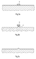
- Fig. 3 shows a corresponding situation for a much smaller size of the dot 4.
- the dot 4 will flake off the surface prior to the finalization of the etching process and accordingly in Fig. 3c ) also in the core area of the dot 4 the etching reaches a certain depth.
- the controlled dot size does not only influence the averaged etch depth by the ratio of the surface covered by the dots 4 but also the factual etch depth in between a non-etched state and a fully-etched state. This by controlling the timing for flaking off the dots 4 from the surface.
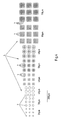
- dots with dot sizes of 20 ⁇ m, 30 ⁇ m, 40 ⁇ m, 48 ⁇ m, 58 ⁇ m, 68 ⁇ m, 80 ⁇ m and 110 ⁇ m are represented.
- the dot sizes of 20 ⁇ m, 30 ⁇ m and 40 ⁇ m are obtained by varying the size of the printing points 7.
- the size of the dots is controlled by composing the dots 4 from four printing points 7 and additionally controlling the size of the printing points 7.
- the size of the dots 4 is controlled by composing them of 16 printing points 7 and again controlling additionally the size of the printing points 7.
- the average etching depth can be controlled also by controlling the density of the dots 4 by modifying the distance in between them.
- the printing points 7 are jetted by ink-jet printing heads.
- Modern ink-jet printing heads can jet printing points of ink or wax with variable sizes, e.g. in between 20 ⁇ m and 40 ⁇ m, and of course can be controlled to compose dots 7 out of a plurality of printing points 7.
Landscapes
- Engineering & Computer Science (AREA)
- Chemical & Material Sciences (AREA)
- Mechanical Engineering (AREA)
- Manufacturing & Machinery (AREA)
- Chemical Kinetics & Catalysis (AREA)
- General Chemical & Material Sciences (AREA)
- Materials Engineering (AREA)
- Metallurgy (AREA)
- Organic Chemistry (AREA)
- Manufacture Or Reproduction Of Printing Formes (AREA)
- Ink Jet (AREA)
Description
- The subject matter of the invention relates to a method for printing stencil and structuring a surface by etching, the method comprising: printing an etch resistant layer of the stencil by jetting etch resistant points, printing the etch resistant layer in areas of intentionally reduced etch depth with at least partially isolated dots.
- Stencils for structuring a surface by etching are used for structuring the surface of metallic substrates. Such metallic substrates could comprise molds, e.g. injection molds, or embossing rollers.
- Prior to the treatment of etching the stencil is applied on the surface of the metallic substrate. The stencil might be either directly printed on the metallic surface or printed on a stencil carrier and then transferred to the surface to be treated.
- In general, etching a surface covered by a stencil is to be understood as constituting a binary treatment. Either the surface is covered by the stencil or not. Accordingly controlling the etch depth to obtain different etch depths despite of the same etch treatment requires additional measures. One is described in the European patent application with the file number
131194261.7 -
GB 2 350 321 A -
US 2007/0166652 A1 discloses a method for applying an etch-resistant stencil on a surface of a substrate and subsequently etching the substrate, generating a textured mold pattern on the surface. -
EP 1 251 398 A2 refers to using an ink-jet printhead to deposit a mask on a surface for subsequent etching, making use of temperature control of the surface to solidity liquid droplets. - In
GB 2 241 352 A - It is also known from the prior art to control the etch depth by making use of the fact that the etch resistant stencil layer will get undercutted during etching. The prior art describes stencil layers comprising at least partially isolated etch resistant dots in areas of potentially reduced etch depth. By this measure at least the averaged etch depth can be controlled by distributing the dots with a controlled density or distance in between the dots. In case the undercutting during the etching results in flaking off the dots from the surface not only the average depth but also the actual depth can be controlled.
- In the prior art the etch resistant dots are identical with an etch resistant point printed as part of a matrix and accordingly cover a zone of the surface with a fixed size. Accordingly the control of the etch depth is determined by the resolution of the printing process.
- To delimit the at least partially isolated etch resistant dots in areas of intentionally reduced etch depth from other areas of the stencil area such dots are understood to cover a zone, i.e. a surface area, reduced by at least 20 per cent due to undercutting in the course of the etching.
- It is an object of the invention to improve the stencil for structuring a surface by etching known from the prior art in a way that the etch depth can be better controlled.
- At least some of the etch resistant dots cover zones with controlled varying size. By varying the size of the etch resistant dots first the proportion of the undercutting effect and thereby the average etch depth is controlled. Second, the period within which the dots are flaking off is controlled. Thereby the actual etch depth as well as the average etch depth is controlled.
- According to a further measure the dots are composed by at least two points. Composing one dot by at least two more or less overlapping points allows the printing of dots with various sizes.
- Alternatively or cumulatively the points can have a controlled varying size thereby single points may constitute dots covering zones with controlled varying size.
- Finally the average reduced etch depth is controlled again alternatively or cumulatively by dots having controlled varying distances. By controlling the distances the density of the dots is controlled and thus the average etch depth in the area of the intentionally reduced etch depth.
- The invention relates to a method for printing a stencil, the method comprising: printing an etch resistant layer of the stencil by jetting etch resistant points; and printing the etch resistant layer in areas of intentionally reduced etch depth with at least partially isolated dots.
- For the problems of the known methods for printing a stencil it can be referred to the statements above concerning the stencil for structuring a surface by etching.
- According to the invention the method further comprises: printing at least some of the etch resistant dots covering zones with varying controlled size to control the actual etch depth and the average etch depth. For the advantages of the inventive solution it can be again referred to the statements with respect to the stencil above.
- A first possibility to further improve the inventive method is by printing the dots by jetting at least two points. Jetting at least two points of etch resistant substances, e.g. ink or wax, easily enables the printing of etch resistant dots covering zones with varying controlled size.
- Alternatively or cumulatively the method further comprises printing the dots by jetting points with controlled varying size. Modern print heads for jetting allow a size of the actual point to be jetted.
- Finally the inventive method is further improved by alternatively or cumulatively comprising the step of printing the dots by jetting points with controlled varying distances.
- There are a multitude of possibilities to implement and improve the present invention. Some of these possibilities are described in the following with reference to the following Figures. In these Figures
- Fig. 1
- shows an embodiment of an stencil for structuring a surface by etching with areas of intentionally reduced etch depth,
- Fig. 2a)-c)
- shows a first embodiment of an isolated dot at the part of an etch resistant stencil layer in the course of an etch process,
- Fig. 3a)-c)
- shows a second embodiment of an isolated dot at the part of an etch resistant stencil layer in the course of an etch process and
- Fig. 4
- a multitude of etch resistant dots as embodiments comprised in an etch resistant stencil layer in the method according to the invention.
-
Fig. 1 of the drawings shows an embodiment of an stencil for structuring a surface by etching. The stencil comprises an etch resistant stencil layer 1 which in this Fig. comprises solidblack areas 2. These solidblack areas 2 are printed as a matrix of etch resistant points fully covering the corresponding area. - The stencil layer 1 also comprises dotted areas 3. These dotted areas 3 are covered at least partially isolated etch
resistant dots 4. The dotted areas 3 are to be identified with areas of intentionally reduced etch depth. - Finally the stencil layer does not cover solid
white areas 5. In these white areas the metallic surface is not protected against etching. Accordingly these are the areas with full etch depth. - In accordance with the invention at least some of the etch
resistant dots 4 in the dotted areas 3 cover zones of the metallic surface with controlled varying size. - In
Fig. 2 of the drawings it is shown how an etchresistant dot 4 with a lateral extension being high compared to the undercutting during etching covers the surface in the course of the etching process. InFig. 2a ) the situation prior to etching is shown. InFig. 2b ) the situation after etching is shown and due to the undercutting 6 the size of the etched zone is 20 per cent or more smaller than the zone covered by thedot 4 prior to etching. InFig. 2c ) the structure of the metallic surface after removing the stencil layer is shown. -
Fig. 3 shows a corresponding situation for a much smaller size of thedot 4. In this situation thedot 4 will flake off the surface prior to the finalization of the etching process and accordingly inFig. 3c ) also in the core area of thedot 4 the etching reaches a certain depth. - Having in mind the situation described with respect to
Figs. 2 and3 the controlled dot size does not only influence the averaged etch depth by the ratio of the surface covered by thedots 4 but also the factual etch depth in between a non-etched state and a fully-etched state. This by controlling the timing for flaking off thedots 4 from the surface. - In
Fig. 4 dots with dot sizes of 20 µm, 30 µm, 40 µm, 48 µm, 58 µm, 68 µm, 80 µm and 110 µm are represented. In this example the dot sizes of 20 µm, 30 µm and 40 µm are obtained by varying the size of the printing points 7. For the dot sizes 48 µm, 58 µm and 68 µm the size of the dots is controlled by composing thedots 4 from fourprinting points 7 and additionally controlling the size of the printing points 7. Also for the dot sizes of 80 µm and 110 µm the size of thedots 4 is controlled by composing them of 16printing points 7 and again controlling additionally the size of the printing points 7. Not specifically shown inFig. 4 is controlling the distances in between thedots 4. It is obvious that the average etching depth can be controlled also by controlling the density of thedots 4 by modifying the distance in between them. - The printing points 7 are jetted by ink-jet printing heads. Modern ink-jet printing heads can jet printing points of ink or wax with variable sizes, e.g. in between 20 µm and 40 µm, and of course can be controlled to compose
dots 7 out of a plurality of printing points 7.
Claims (4)
- Method for printing a stencil and structuring a surface by etching, the method comprising:printing an etch resistant layer of the stencil by jetting etch resistant points,printing the etch resistant layer in areas of intentionally reduced etch depth with at least partially isolated dots,characterized in that,
the method further comprises:printing at least some of the etch resistant dots covering zones with varying controlled size to control the actual etch depth and the average etch depth. - Method according to claim 2,
characterized in that,
the method further comprises printing the dots by jetting at least two points. - Method according to claims 1 or 2,
characterized in that,
the method further comprises printing the dots by jetting points with controlled varying size. - Method according to one of claims 1 to 3,
characterized in that,
the method further comprises printing the dots with controlled varying distances.
Priority Applications (3)
| Application Number | Priority Date | Filing Date | Title |
|---|---|---|---|
| ES14165415.2T ES2607641T3 (en) | 2014-04-22 | 2014-04-22 | Method with a stencil template for structuring a surface by engraving |
| EP14165415.2A EP2937147B1 (en) | 2014-04-22 | 2014-04-22 | Method with a stencil for structuring a surface by etching |
| PT141654152T PT2937147T (en) | 2014-04-22 | 2014-04-22 | Method with a stencil for structuring a surface by etching |
Applications Claiming Priority (1)
| Application Number | Priority Date | Filing Date | Title |
|---|---|---|---|
| EP14165415.2A EP2937147B1 (en) | 2014-04-22 | 2014-04-22 | Method with a stencil for structuring a surface by etching |
Publications (2)
| Publication Number | Publication Date |
|---|---|
| EP2937147A1 EP2937147A1 (en) | 2015-10-28 |
| EP2937147B1 true EP2937147B1 (en) | 2016-11-16 |
Family
ID=50513119
Family Applications (1)
| Application Number | Title | Priority Date | Filing Date |
|---|---|---|---|
| EP14165415.2A Revoked EP2937147B1 (en) | 2014-04-22 | 2014-04-22 | Method with a stencil for structuring a surface by etching |
Country Status (3)
| Country | Link |
|---|---|
| EP (1) | EP2937147B1 (en) |
| ES (1) | ES2607641T3 (en) |
| PT (1) | PT2937147T (en) |
Citations (2)
| Publication number | Priority date | Publication date | Assignee | Title |
|---|---|---|---|---|
| US7147789B1 (en) | 2000-10-19 | 2006-12-12 | Hutchinson Technology Incorporated | Process for control of contours formed by etching substrates |
| US20110024392A1 (en) | 2008-03-27 | 2011-02-03 | Masaki Sato | Ink-jet ink composition for etching resist |
Family Cites Families (5)
| Publication number | Priority date | Publication date | Assignee | Title |
|---|---|---|---|---|
| CA2036424A1 (en) * | 1990-02-23 | 1991-08-24 | Albert C. Chiang | Photopolymer printing plates having a dimpled printing surface |
| JP3642801B2 (en) * | 1994-02-18 | 2005-04-27 | リコー光学株式会社 | EXPOSURE MASK, ITS MANUFACTURING METHOD, SURFACE SHAPE FORMING METHOD USING EXPOSURE MASK, AND EXPOSURE MASK MANUFACTURING APPARATUS |
| GB2350321A (en) * | 1999-05-27 | 2000-11-29 | Patterning Technologies Ltd | Method of forming a masking or spacer pattern on a substrate using inkjet droplet deposition |
| US6872320B2 (en) * | 2001-04-19 | 2005-03-29 | Xerox Corporation | Method for printing etch masks using phase-change materials |
| PT1993849E (en) * | 2006-01-19 | 2010-11-25 | Ikonics Corp | Digital mold texturizing methods |
-
2014
- 2014-04-22 EP EP14165415.2A patent/EP2937147B1/en not_active Revoked
- 2014-04-22 ES ES14165415.2T patent/ES2607641T3/en active Active
- 2014-04-22 PT PT141654152T patent/PT2937147T/en unknown
Patent Citations (2)
| Publication number | Priority date | Publication date | Assignee | Title |
|---|---|---|---|---|
| US7147789B1 (en) | 2000-10-19 | 2006-12-12 | Hutchinson Technology Incorporated | Process for control of contours formed by etching substrates |
| US20110024392A1 (en) | 2008-03-27 | 2011-02-03 | Masaki Sato | Ink-jet ink composition for etching resist |
Also Published As
| Publication number | Publication date |
|---|---|
| PT2937147T (en) | 2016-12-22 |
| ES2607641T3 (en) | 2017-04-03 |
| EP2937147A1 (en) | 2015-10-28 |
Similar Documents
| Publication | Publication Date | Title |
|---|---|---|
| EP1597781B1 (en) | Method for producing a light-emitting device | |
| JP3445352B2 (en) | Print version | |
| WO2007026172A1 (en) | Method of printing | |
| US20210370605A1 (en) | Method for producing a three-dimensional element on a timepiece component | |
| CN104174576B (en) | Manufacturing method and coloring method of coloring material of aluminum material | |
| EP3326830A1 (en) | Printing plate, printed matter, and printing method | |
| JP5904448B2 (en) | Offset printing plate and method for producing the same | |
| JP2011177606A (en) | Decorative printing method | |
| EP3357693A1 (en) | Center drum type gravure printing apparatus, and gravure printing method and method for manufacturing printed article using said apparatus | |
| KR20120061424A (en) | Intaglio Printing Plate Including Supplementary Pattern And Method For Fabricating The Same | |
| EP2937147A1 (en) | Stencil for structuring a surface by etching | |
| US20160263620A1 (en) | Method of making patterned article | |
| WO2017069081A1 (en) | Surface structure for printing base material, and method for manufacturing same | |
| KR101816687B1 (en) | Print media of aluminum and manufacturing method thereby | |
| EP3482937A1 (en) | Method for structuring a surface, gravure printing form or embossing tool and use | |
| CN100391741C (en) | Spray hole sheet | |
| JP6126315B1 (en) | Stencil for forming surface structure by etching | |
| US2315903A (en) | Process of engraving | |
| CN101231361A (en) | Method for manufacturing substrate with thin membrane pattern layer | |
| EP3205499B1 (en) | Method for structuring a surface of a gravure form | |
| US8353575B2 (en) | Nozzle sheet and method for manufacturing the same | |
| US7560223B2 (en) | Fluid ejection device structures and methods therefor | |
| US2373060A (en) | Die stamping | |
| KR101460072B1 (en) | Method of manufacturing micro pattern having high resolution | |
| KR100533138B1 (en) | Ink jet printer head and fabrication method |
Legal Events
| Date | Code | Title | Description |
|---|---|---|---|
| REG | Reference to a national code |
Ref country code: DE Ref legal event code: R138 Ref document number: 202014011018 Country of ref document: DE Free format text: GERMAN DOCUMENT NUMBER IS 602014004824 |
|
| PUAI | Public reference made under article 153(3) epc to a published international application that has entered the european phase |
Free format text: ORIGINAL CODE: 0009012 |
|
| AK | Designated contracting states |
Kind code of ref document: A1 Designated state(s): AL AT BE BG CH CY CZ DE DK EE ES FI FR GB GR HR HU IE IS IT LI LT LU LV MC MK MT NL NO PL PT RO RS SE SI SK SM TR |
|
| AX | Request for extension of the european patent |
Extension state: BA ME |
|
| 17P | Request for examination filed |
Effective date: 20160210 |
|
| RBV | Designated contracting states (corrected) |
Designated state(s): AL AT BE BG CH CY CZ DE DK EE ES FI FR GB GR HR HU IE IS IT LI LT LU LV MC MK MT NL NO PL PT RO RS SE SI SK SM TR |
|
| GRAP | Despatch of communication of intention to grant a patent |
Free format text: ORIGINAL CODE: EPIDOSNIGR1 |
|
| INTG | Intention to grant announced |
Effective date: 20160708 |
|
| GRAS | Grant fee paid |
Free format text: ORIGINAL CODE: EPIDOSNIGR3 |
|
| GRAA | (expected) grant |
Free format text: ORIGINAL CODE: 0009210 |
|
| AK | Designated contracting states |
Kind code of ref document: B1 Designated state(s): AL AT BE BG CH CY CZ DE DK EE ES FI FR GB GR HR HU IE IS IT LI LT LU LV MC MK MT NL NO PL PT RO RS SE SI SK SM TR |
|
| REG | Reference to a national code |
Ref country code: GB Ref legal event code: FG4D |
|
| REG | Reference to a national code |
Ref country code: CH Ref legal event code: EP |
|
| REG | Reference to a national code |
Ref country code: IE Ref legal event code: FG4D |
|
| REG | Reference to a national code |
Ref country code: AT Ref legal event code: REF Ref document number: 845412 Country of ref document: AT Kind code of ref document: T Effective date: 20161215 |
|
| REG | Reference to a national code |
Ref country code: DE Ref legal event code: R096 Ref document number: 602014004824 Country of ref document: DE Ref country code: PT Ref legal event code: SC4A Ref document number: 2937147 Country of ref document: PT Date of ref document: 20161222 Kind code of ref document: T Free format text: AVAILABILITY OF NATIONAL TRANSLATION Effective date: 20161214 |
|
| REG | Reference to a national code |
Ref country code: NL Ref legal event code: FP |
|
| PG25 | Lapsed in a contracting state [announced via postgrant information from national office to epo] |
Ref country code: LV Free format text: LAPSE BECAUSE OF FAILURE TO SUBMIT A TRANSLATION OF THE DESCRIPTION OR TO PAY THE FEE WITHIN THE PRESCRIBED TIME-LIMIT Effective date: 20161116 |
|
| REG | Reference to a national code |
Ref country code: LT Ref legal event code: MG4D |
|
| REG | Reference to a national code |
Ref country code: AT Ref legal event code: MK05 Ref document number: 845412 Country of ref document: AT Kind code of ref document: T Effective date: 20161116 |
|
| REG | Reference to a national code |
Ref country code: FR Ref legal event code: PLFP Year of fee payment: 4 |
|
| PG25 | Lapsed in a contracting state [announced via postgrant information from national office to epo] |
Ref country code: LT Free format text: LAPSE BECAUSE OF FAILURE TO SUBMIT A TRANSLATION OF THE DESCRIPTION OR TO PAY THE FEE WITHIN THE PRESCRIBED TIME-LIMIT Effective date: 20161116 Ref country code: SE Free format text: LAPSE BECAUSE OF FAILURE TO SUBMIT A TRANSLATION OF THE DESCRIPTION OR TO PAY THE FEE WITHIN THE PRESCRIBED TIME-LIMIT Effective date: 20161116 Ref country code: GR Free format text: LAPSE BECAUSE OF FAILURE TO SUBMIT A TRANSLATION OF THE DESCRIPTION OR TO PAY THE FEE WITHIN THE PRESCRIBED TIME-LIMIT Effective date: 20170217 Ref country code: NO Free format text: LAPSE BECAUSE OF FAILURE TO SUBMIT A TRANSLATION OF THE DESCRIPTION OR TO PAY THE FEE WITHIN THE PRESCRIBED TIME-LIMIT Effective date: 20170216 |
|
| PG25 | Lapsed in a contracting state [announced via postgrant information from national office to epo] |
Ref country code: FI Free format text: LAPSE BECAUSE OF FAILURE TO SUBMIT A TRANSLATION OF THE DESCRIPTION OR TO PAY THE FEE WITHIN THE PRESCRIBED TIME-LIMIT Effective date: 20161116 Ref country code: AT Free format text: LAPSE BECAUSE OF FAILURE TO SUBMIT A TRANSLATION OF THE DESCRIPTION OR TO PAY THE FEE WITHIN THE PRESCRIBED TIME-LIMIT Effective date: 20161116 Ref country code: RS Free format text: LAPSE BECAUSE OF FAILURE TO SUBMIT A TRANSLATION OF THE DESCRIPTION OR TO PAY THE FEE WITHIN THE PRESCRIBED TIME-LIMIT Effective date: 20161116 Ref country code: HR Free format text: LAPSE BECAUSE OF FAILURE TO SUBMIT A TRANSLATION OF THE DESCRIPTION OR TO PAY THE FEE WITHIN THE PRESCRIBED TIME-LIMIT Effective date: 20161116 Ref country code: PL Free format text: LAPSE BECAUSE OF FAILURE TO SUBMIT A TRANSLATION OF THE DESCRIPTION OR TO PAY THE FEE WITHIN THE PRESCRIBED TIME-LIMIT Effective date: 20161116 |
|
| PG25 | Lapsed in a contracting state [announced via postgrant information from national office to epo] |
Ref country code: CZ Free format text: LAPSE BECAUSE OF FAILURE TO SUBMIT A TRANSLATION OF THE DESCRIPTION OR TO PAY THE FEE WITHIN THE PRESCRIBED TIME-LIMIT Effective date: 20161116 Ref country code: RO Free format text: LAPSE BECAUSE OF FAILURE TO SUBMIT A TRANSLATION OF THE DESCRIPTION OR TO PAY THE FEE WITHIN THE PRESCRIBED TIME-LIMIT Effective date: 20161116 Ref country code: DK Free format text: LAPSE BECAUSE OF FAILURE TO SUBMIT A TRANSLATION OF THE DESCRIPTION OR TO PAY THE FEE WITHIN THE PRESCRIBED TIME-LIMIT Effective date: 20161116 Ref country code: EE Free format text: LAPSE BECAUSE OF FAILURE TO SUBMIT A TRANSLATION OF THE DESCRIPTION OR TO PAY THE FEE WITHIN THE PRESCRIBED TIME-LIMIT Effective date: 20161116 Ref country code: SK Free format text: LAPSE BECAUSE OF FAILURE TO SUBMIT A TRANSLATION OF THE DESCRIPTION OR TO PAY THE FEE WITHIN THE PRESCRIBED TIME-LIMIT Effective date: 20161116 |
|
| REG | Reference to a national code |
Ref country code: DE Ref legal event code: R026 Ref document number: 602014004824 Country of ref document: DE |
|
| PLBI | Opposition filed |
Free format text: ORIGINAL CODE: 0009260 |
|
| PG25 | Lapsed in a contracting state [announced via postgrant information from national office to epo] |
Ref country code: BE Free format text: LAPSE BECAUSE OF FAILURE TO SUBMIT A TRANSLATION OF THE DESCRIPTION OR TO PAY THE FEE WITHIN THE PRESCRIBED TIME-LIMIT Effective date: 20161116 Ref country code: SM Free format text: LAPSE BECAUSE OF FAILURE TO SUBMIT A TRANSLATION OF THE DESCRIPTION OR TO PAY THE FEE WITHIN THE PRESCRIBED TIME-LIMIT Effective date: 20161116 Ref country code: BG Free format text: LAPSE BECAUSE OF FAILURE TO SUBMIT A TRANSLATION OF THE DESCRIPTION OR TO PAY THE FEE WITHIN THE PRESCRIBED TIME-LIMIT Effective date: 20170216 |
|
| PLAX | Notice of opposition and request to file observation + time limit sent |
Free format text: ORIGINAL CODE: EPIDOSNOBS2 |
|
| 26 | Opposition filed |
Opponent name: IKONICS CORPORATION Effective date: 20170816 |
|
| PG25 | Lapsed in a contracting state [announced via postgrant information from national office to epo] |
Ref country code: SI Free format text: LAPSE BECAUSE OF FAILURE TO SUBMIT A TRANSLATION OF THE DESCRIPTION OR TO PAY THE FEE WITHIN THE PRESCRIBED TIME-LIMIT Effective date: 20161116 |
|
| REG | Reference to a national code |
Ref country code: CH Ref legal event code: PL |
|
| REG | Reference to a national code |
Ref country code: IE Ref legal event code: MM4A |
|
| PLBB | Reply of patent proprietor to notice(s) of opposition received |
Free format text: ORIGINAL CODE: EPIDOSNOBS3 |
|
| PG25 | Lapsed in a contracting state [announced via postgrant information from national office to epo] |
Ref country code: MC Free format text: LAPSE BECAUSE OF FAILURE TO SUBMIT A TRANSLATION OF THE DESCRIPTION OR TO PAY THE FEE WITHIN THE PRESCRIBED TIME-LIMIT Effective date: 20161116 |
|
| PG25 | Lapsed in a contracting state [announced via postgrant information from national office to epo] |
Ref country code: LI Free format text: LAPSE BECAUSE OF NON-PAYMENT OF DUE FEES Effective date: 20170430 Ref country code: LU Free format text: LAPSE BECAUSE OF NON-PAYMENT OF DUE FEES Effective date: 20170422 Ref country code: CH Free format text: LAPSE BECAUSE OF NON-PAYMENT OF DUE FEES Effective date: 20170430 |
|
| REG | Reference to a national code |
Ref country code: FR Ref legal event code: PLFP Year of fee payment: 5 |
|
| PG25 | Lapsed in a contracting state [announced via postgrant information from national office to epo] |
Ref country code: IE Free format text: LAPSE BECAUSE OF NON-PAYMENT OF DUE FEES Effective date: 20170422 |
|
| PGFP | Annual fee paid to national office [announced via postgrant information from national office to epo] |
Ref country code: TR Payment date: 20180316 Year of fee payment: 5 Ref country code: PT Payment date: 20180322 Year of fee payment: 5 |
|
| PGFP | Annual fee paid to national office [announced via postgrant information from national office to epo] |
Ref country code: NL Payment date: 20180420 Year of fee payment: 5 |
|
| PGFP | Annual fee paid to national office [announced via postgrant information from national office to epo] |
Ref country code: ES Payment date: 20180502 Year of fee payment: 5 Ref country code: DE Payment date: 20180420 Year of fee payment: 5 |
|
| PGFP | Annual fee paid to national office [announced via postgrant information from national office to epo] |
Ref country code: FR Payment date: 20180424 Year of fee payment: 5 Ref country code: IT Payment date: 20180430 Year of fee payment: 5 |
|
| PG25 | Lapsed in a contracting state [announced via postgrant information from national office to epo] |
Ref country code: MT Free format text: LAPSE BECAUSE OF NON-PAYMENT OF DUE FEES Effective date: 20170422 |
|
| PGFP | Annual fee paid to national office [announced via postgrant information from national office to epo] |
Ref country code: GB Payment date: 20180420 Year of fee payment: 5 |
|
| RDAF | Communication despatched that patent is revoked |
Free format text: ORIGINAL CODE: EPIDOSNREV1 |
|
| STAA | Information on the status of an ep patent application or granted ep patent |
Free format text: STATUS: THE PATENT HAS BEEN GRANTED |
|
| REG | Reference to a national code |
Ref country code: DE Ref legal event code: R064 Ref document number: 602014004824 Country of ref document: DE Ref country code: DE Ref legal event code: R103 Ref document number: 602014004824 Country of ref document: DE |
|
| RDAG | Patent revoked |
Free format text: ORIGINAL CODE: 0009271 |
|
| STAA | Information on the status of an ep patent application or granted ep patent |
Free format text: STATUS: PATENT REVOKED |
|
| 27W | Patent revoked |
Effective date: 20190309 |
|
| GBPR | Gb: patent revoked under art. 102 of the ep convention designating the uk as contracting state |
Effective date: 20190309 |
|
| PG25 | Lapsed in a contracting state [announced via postgrant information from national office to epo] |
Ref country code: MK Free format text: LAPSE BECAUSE OF FAILURE TO SUBMIT A TRANSLATION OF THE DESCRIPTION OR TO PAY THE FEE WITHIN THE PRESCRIBED TIME-LIMIT Effective date: 20161116 |
|
| PG25 | Lapsed in a contracting state [announced via postgrant information from national office to epo] |
Ref country code: CY Free format text: LAPSE BECAUSE OF FAILURE TO SUBMIT A TRANSLATION OF THE DESCRIPTION OR TO PAY THE FEE WITHIN THE PRESCRIBED TIME-LIMIT Effective date: 20161116 |
|
| PG25 | Lapsed in a contracting state [announced via postgrant information from national office to epo] |
Ref country code: AL Free format text: LAPSE BECAUSE OF FAILURE TO SUBMIT A TRANSLATION OF THE DESCRIPTION OR TO PAY THE FEE WITHIN THE PRESCRIBED TIME-LIMIT Effective date: 20161116 Ref country code: IS Free format text: LAPSE BECAUSE OF FAILURE TO SUBMIT A TRANSLATION OF THE DESCRIPTION OR TO PAY THE FEE WITHIN THE PRESCRIBED TIME-LIMIT Effective date: 20170316 |