EP2933846A1 - Ensemble de condensation linéaire et son procédé de fabrication - Google Patents
Ensemble de condensation linéaire et son procédé de fabrication Download PDFInfo
- Publication number
- EP2933846A1 EP2933846A1 EP13863342.5A EP13863342A EP2933846A1 EP 2933846 A1 EP2933846 A1 EP 2933846A1 EP 13863342 A EP13863342 A EP 13863342A EP 2933846 A1 EP2933846 A1 EP 2933846A1
- Authority
- EP
- European Patent Office
- Prior art keywords
- strip
- linear condensation
- solar cells
- solar cell
- shaped
- Prior art date
- Legal status (The legal status is an assumption and is not a legal conclusion. Google has not performed a legal analysis and makes no representation as to the accuracy of the status listed.)
- Withdrawn
Links
Images


Classifications
-
- H—ELECTRICITY
- H10—SEMICONDUCTOR DEVICES; ELECTRIC SOLID-STATE DEVICES NOT OTHERWISE PROVIDED FOR
- H10F—INORGANIC SEMICONDUCTOR DEVICES SENSITIVE TO INFRARED RADIATION, LIGHT, ELECTROMAGNETIC RADIATION OF SHORTER WAVELENGTH OR CORPUSCULAR RADIATION
- H10F77/00—Constructional details of devices covered by this subclass
- H10F77/40—Optical elements or arrangements
- H10F77/42—Optical elements or arrangements directly associated or integrated with photovoltaic cells, e.g. light-reflecting means or light-concentrating means
- H10F77/484—Refractive light-concentrating means, e.g. lenses
-
- G—PHYSICS
- G02—OPTICS
- G02B—OPTICAL ELEMENTS, SYSTEMS OR APPARATUS
- G02B19/00—Condensers, e.g. light collectors or similar non-imaging optics
- G02B19/0033—Condensers, e.g. light collectors or similar non-imaging optics characterised by the use
- G02B19/0038—Condensers, e.g. light collectors or similar non-imaging optics characterised by the use for use with ambient light
- G02B19/0042—Condensers, e.g. light collectors or similar non-imaging optics characterised by the use for use with ambient light for use with direct solar radiation
-
- H—ELECTRICITY
- H10—SEMICONDUCTOR DEVICES; ELECTRIC SOLID-STATE DEVICES NOT OTHERWISE PROVIDED FOR
- H10F—INORGANIC SEMICONDUCTOR DEVICES SENSITIVE TO INFRARED RADIATION, LIGHT, ELECTROMAGNETIC RADIATION OF SHORTER WAVELENGTH OR CORPUSCULAR RADIATION
- H10F10/00—Individual photovoltaic cells, e.g. solar cells
- H10F10/10—Individual photovoltaic cells, e.g. solar cells having potential barriers
- H10F10/14—Photovoltaic cells having only PN homojunction potential barriers
-
- H—ELECTRICITY
- H10—SEMICONDUCTOR DEVICES; ELECTRIC SOLID-STATE DEVICES NOT OTHERWISE PROVIDED FOR
- H10F—INORGANIC SEMICONDUCTOR DEVICES SENSITIVE TO INFRARED RADIATION, LIGHT, ELECTROMAGNETIC RADIATION OF SHORTER WAVELENGTH OR CORPUSCULAR RADIATION
- H10F19/00—Integrated devices, or assemblies of multiple devices, comprising at least one photovoltaic cell covered by group H10F10/00, e.g. photovoltaic modules
- H10F19/80—Encapsulations or containers for integrated devices, or assemblies of multiple devices, having photovoltaic cells
-
- H—ELECTRICITY
- H10—SEMICONDUCTOR DEVICES; ELECTRIC SOLID-STATE DEVICES NOT OTHERWISE PROVIDED FOR
- H10F—INORGANIC SEMICONDUCTOR DEVICES SENSITIVE TO INFRARED RADIATION, LIGHT, ELECTROMAGNETIC RADIATION OF SHORTER WAVELENGTH OR CORPUSCULAR RADIATION
- H10F19/00—Integrated devices, or assemblies of multiple devices, comprising at least one photovoltaic cell covered by group H10F10/00, e.g. photovoltaic modules
- H10F19/90—Structures for connecting between photovoltaic cells, e.g. interconnections or insulating spacers
- H10F19/902—Structures for connecting between photovoltaic cells, e.g. interconnections or insulating spacers for series or parallel connection of photovoltaic cells
-
- H—ELECTRICITY
- H10—SEMICONDUCTOR DEVICES; ELECTRIC SOLID-STATE DEVICES NOT OTHERWISE PROVIDED FOR
- H10F—INORGANIC SEMICONDUCTOR DEVICES SENSITIVE TO INFRARED RADIATION, LIGHT, ELECTROMAGNETIC RADIATION OF SHORTER WAVELENGTH OR CORPUSCULAR RADIATION
- H10F71/00—Manufacture or treatment of devices covered by this subclass
- H10F71/121—The active layers comprising only Group IV materials
-
- H—ELECTRICITY
- H10—SEMICONDUCTOR DEVICES; ELECTRIC SOLID-STATE DEVICES NOT OTHERWISE PROVIDED FOR
- H10F—INORGANIC SEMICONDUCTOR DEVICES SENSITIVE TO INFRARED RADIATION, LIGHT, ELECTROMAGNETIC RADIATION OF SHORTER WAVELENGTH OR CORPUSCULAR RADIATION
- H10F71/00—Manufacture or treatment of devices covered by this subclass
- H10F71/133—Providing edge isolation
-
- H—ELECTRICITY
- H10—SEMICONDUCTOR DEVICES; ELECTRIC SOLID-STATE DEVICES NOT OTHERWISE PROVIDED FOR
- H10F—INORGANIC SEMICONDUCTOR DEVICES SENSITIVE TO INFRARED RADIATION, LIGHT, ELECTROMAGNETIC RADIATION OF SHORTER WAVELENGTH OR CORPUSCULAR RADIATION
- H10F71/00—Manufacture or treatment of devices covered by this subclass
- H10F71/136—Singulating, e.g. dicing
-
- H—ELECTRICITY
- H10—SEMICONDUCTOR DEVICES; ELECTRIC SOLID-STATE DEVICES NOT OTHERWISE PROVIDED FOR
- H10W—GENERIC PACKAGES, INTERCONNECTIONS, CONNECTORS OR OTHER CONSTRUCTIONAL DETAILS OF DEVICES COVERED BY CLASS H10
- H10W90/00—Package configurations
-
- G—PHYSICS
- G02—OPTICS
- G02B—OPTICAL ELEMENTS, SYSTEMS OR APPARATUS
- G02B3/00—Simple or compound lenses
- G02B3/0006—Arrays
- G02B3/0037—Arrays characterized by the distribution or form of lenses
- G02B3/005—Arrays characterized by the distribution or form of lenses arranged along a single direction only, e.g. lenticular sheets
-
- Y—GENERAL TAGGING OF NEW TECHNOLOGICAL DEVELOPMENTS; GENERAL TAGGING OF CROSS-SECTIONAL TECHNOLOGIES SPANNING OVER SEVERAL SECTIONS OF THE IPC; TECHNICAL SUBJECTS COVERED BY FORMER USPC CROSS-REFERENCE ART COLLECTIONS [XRACs] AND DIGESTS
- Y02—TECHNOLOGIES OR APPLICATIONS FOR MITIGATION OR ADAPTATION AGAINST CLIMATE CHANGE
- Y02E—REDUCTION OF GREENHOUSE GAS [GHG] EMISSIONS, RELATED TO ENERGY GENERATION, TRANSMISSION OR DISTRIBUTION
- Y02E10/00—Energy generation through renewable energy sources
- Y02E10/50—Photovoltaic [PV] energy
- Y02E10/52—PV systems with concentrators
-
- Y—GENERAL TAGGING OF NEW TECHNOLOGICAL DEVELOPMENTS; GENERAL TAGGING OF CROSS-SECTIONAL TECHNOLOGIES SPANNING OVER SEVERAL SECTIONS OF THE IPC; TECHNICAL SUBJECTS COVERED BY FORMER USPC CROSS-REFERENCE ART COLLECTIONS [XRACs] AND DIGESTS
- Y02—TECHNOLOGIES OR APPLICATIONS FOR MITIGATION OR ADAPTATION AGAINST CLIMATE CHANGE
- Y02E—REDUCTION OF GREENHOUSE GAS [GHG] EMISSIONS, RELATED TO ENERGY GENERATION, TRANSMISSION OR DISTRIBUTION
- Y02E10/00—Energy generation through renewable energy sources
- Y02E10/50—Photovoltaic [PV] energy
- Y02E10/547—Monocrystalline silicon PV cells
Definitions
- the invention belongs to the technical field of solar utilization, in particular to a linear condensation assembly and a manufacturing process thereof.
- a photovoltaic solar cell module comprises grading testing of common crystalline silicon solar cell pieces, single welding and series welding of the cell pieces, stacking, lamination and curing, and assembly of an aluminum alloy frame.
- the final photovoltaic solar cell module product has high cost, so that the cost of the photovoltaic power generation at current stage is several times greater than that of the conventional power generation, thus limiting large-scale application of photovoltaic power generation technology and restricting development of the entire industry.
- the purpose of the invention is to provide a linear condensation assembly capable of effectively reducing consumption of cell piece of a common photovoltaic module and further reducing production cost of the photovoltaic module as well as a manufacturing process thereof.
- the cutting of the solar cells is divided into scribing and segmenting, the solar cells are scribed by laser or diamond to form 50 to 150 ⁇ m depth on the solar cells, and then the solar cells are segmented along scribing positions by a segmenting device to form strip-shaped solar cells.
- the back of the solar cells is scribed by laser or diamond, and then the solar cells are segmented along cutting positions by a segmenting device to form the strip-shaped solar cells.
- the solar cell cut at a certain depth is placed on a soft rubber pad, with the side of the solar cell with scribing incision facing downward and the other side being provided with a layer of protective film; a scrollable rigid roller is placed on the protective film, and the rigid roller rolls along the direction perpendicular to the scribing direction of the solar cell; and the solar cell pieces are rolled by the rigid roller and disconnected from the incision to form strip-shaped solar cells, and after the solar cell pieces are disconnected into strip-shaped solar cells, the protective film on the front of the solar cell is removed, and the strip-shaped solar cells are placed at certain intervals by a strip-shaped solar cell pickup device.
- the solar cell cut at a certain depth is placed on a cell fixing platform with the back facing up, and fixed and adsorbed by negative pressure; a pneumatic clamping gripper arranged at the cell fixing platform clamps one side of the solar cell and inches the solar cell at a certain beat under the action of an inching drive mechanism; the other side of the solar cell is clamped at the clamping position of a segmenting mechanism, and the clamping position acts downward under the action of a segmenting cylinder to disconnect the solar cell along the scribing position and complete segmenting of the solar cell pieces; and the segmented strip-shaped solar cells are placed at certain intervals by the clamping position of the segmenting mechanism through a step motor.
- step c) In the manufacturing process of a linear condensation assembly of the invention, in the step c), firstly, lower solder strips with the same number as the main grid lines of the welded strip-shaped solar cells are placed in a solder strip placement slot on a grid solar cell piece welding platform, vacuum adsorption holes arranged in the solder strip placement slot correspond to the lower solder strips, and the lower solder strips are fixed by adsorption; secondly, the strip-shaped solar cells cut as per the step b) are placed on the grid solar cell piece welding platform at a certain fixed interval, the upper end faces of the lower solder strips contact positive poles of corresponding strip-shaped solar cells, the vacuum adsorption holes on the grid solar cell piece welding platform correspond to the placed strip-shaped solar cells, and the strip-shaped solar cells are fixed by adsorption; thirdly, upper solder strips are placed on negative main grid lines corresponding to the strip-shaped solar cells, an upper fire resistant hold-down mechanism moves downwards, and hold-down strips of the hold-down mechanism are used to compress
- the linear condensation glass panel is properly placed, and a layer of cell sealing material is applied on the linear condensation glass panel, then the cell strings are placed, and a positioning device is used to align centers of the strip-shaped solar cells of the cell strings with optical construction centers of all curved linear condensation surfaces on the linear condensation glass panel, after alignment, a layer of cell sealing material and a layer of back panel material are successively applied.
- the optical construction centers of the curved linear condensation surfaces on the linear condensation glass panel are identified by two position sensors, the position sensors move along optical structure surfaces of the curved linear condensation surfaces of the linear condensation glass panel to judge the highest points of the curved linear condensation surfaces, and then judge the center lines of the curved linear condensation surfaces, the strip-shaped solar cells move back and forth or left to right or rotate through strip-shaped cell position moving devices, and the strip-shaped cell position moving devices move accordingly based on central positions of the curved linear condensation surfaces of the linear condensation glass panel identified by the position sensors and deviation values to correct positions of the strip-shaped solar cells so that the centers are aligned with the optical construction centers of the curved linear condensation surfaces of the linear condensation glass panel.
- the linear condensation glass panel gathers and projects solar rays received on the cell strings, width of linear condensing rays formed after the curved linear condensation surfaces of the linear condensation glass panel gather solar rays is not more than width of the strip-shaped solar cells in the cell strings, or the width of the linear condensing rays formed after the curved linear condensation surfaces of the linear condensation glass panel gather solar rays is not less than the width of the strip-shaped solar cells in the cell strings.
- the width of linear condensing rays formed after the curved linear condensation surfaces of the linear condensation glass panel gather solar rays is consistent with the width of the strip-shaped solar cells in the cell strings, and the spacing between the two adjacent strip-shaped solar cells is consistent with the spacing between the linear condensing rays formed by adjacent curved linear condensation surfaces.
- receiving surfaces on upper surfaces of the strip-shaped solar cells of the grid solar cell pieces are on the same plane
- the receiving surfaces formed by upper surfaces of the grid solar cell pieces in the cell strings are on the same plane
- the receiving surfaces formed by upper surfaces of the cell strings are on the same plane.
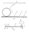
- a linear condensation assembly comprises a linear condensation glass panel, a sealing material layer, solar cells and a back panel; the upper part of the condensation glass panel is of a curved linear arc-shaped condensation surface array; the solar cells comprise multiple strip-shaped solar cells and solders strips; the strip-shaped solar cells vertically correspond to curved linear arc-shaped condensation surfaces of the linear condensation glass panel; the multiple strip-shaped solar cells are welded and connected on the solder strips to form grid solar cell pieces; and the linear condensation glass panel, the sealing material layer, the solar cells and the back panel are laminated to form a linear condensation assembly.
- an upper end surface of the linear condensation glass panel is lens condensing and refracting surface, and a lower end thereof is a flat surface;
- the lens extends transversally and is of strip shape, the linear condensation glass panel is capable of refracting mutually parallel incident rays onto the grid solar cell pieces arranged below the linear condensation glass panel so as to form linear condensation rays;
- the vertical distance from the contact point between any incident ray and the lens condensing and refracting surface to the corresponding lens vertical central axis on the linear condensation glass panel is x, the vertical distance from a projection point formed after the incident ray is refracted onto a corresponding strip-shaped solar cell through the lens to the center line in the length direction of the linear condensation ray is m, the vertical distance from the edge of the lens condensing and refracting surface to the vertical central axis is a, and the vertical distance from the projection point of the incident ray refracted through the edge of the lens condensing and re
- variable x is the transversal distance from any point on the lens condensing and refracting surface to the vertical central axis on the vertical surface
- variable y is the vertical distance from the point to the plane where both edges of the lens condensing and refracting surface are located.
- the vertical distance a from the edge of the lens condensing and refracting surface to the vertical central axis and the vertical distance b from the projection point of the incident ray refracted through the lens condensing and refracting surface on the strip-shaped solar cell to the center line in the length direction of the linear condensation ray meet the following condition: 1 ⁇ a/b ⁇ 10.
- the vertical distance from the edge of the lens condensing and refracting surface to the lower flat surface below the linear condensation glass panel is h, and the lower end surface of the linear condensation glass panel is accordingly connected with the upper end surface of the strip-shaped solar cell.
- the linear condensation glass panel is symmetrical or asymmetrical along the vertical central axis.
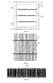
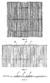
- the surface of the solar cell comprises multiple annular fine grid lines equally spaced on the solar cell and at least two main grid lines perpendicular to the annular fine grid lines, the spacing between two adjacent annular fine grid lines is 0.1mm to 2mm, and each annual fine grid line is 1mm to 10mm wide.
- the main grid lines are disconnected at the clearance between two adjacent annular fine grid lines, and are divided into multiple separate units matched with the annular fine grid lines.
- the scribing position is at the clearance between the two adjacent annular fine grid lines; the width of the annular fine grid line is less than that of cut strip-shaped solar cells.
- each annular fine grid line corresponds to a strip-shaped solar cell, and the annular fine grid lines are uniformly distributed at edges of corresponding strip-shaped solar cells.
- the annular fine grid lines close to left and right edges on the solar cell are of the same design and symmetrically arranged, and the annular fine grid lines therebetween are of the same design and of rectangular shape.
- the grid solar cell pieces include multiple equally spaced strip-shaped solar cells, and the strip-shaped solar cells are electrically connected by solder strips composed of multiple solder strip sections connected between two adjacent strip-shaped solar cells, one end of each solder strip section is connected to the upper end of one strip-shaped solar cell, and the other end is connected to the lower end of the other strip-shaped solar cell connected thereto; and the solder strip sections are successively connected so that multiple strip-shaped solar cells are electrically connected in series.
- solder strip sections are of Z shape.
- scribing, segmenting and welding processes for common crystalline silicon solar cell pieces are added in the manufacturing process so that common crystalline silicon solar cells can form grid solar cell pieces composed of strip-shaped solar cells at certain fixed interval, and then the grid solar cell pieces are subject to subsequent stacking, lamination and curing processes under the cooperation of a special linear condensation glass panel to obtain a photovoltaic module finally.
- the linear condensation photovoltaic module manufactured by the process of the invention can reduce consumption of cell piece of common photovoltaic module, thus reducing manufacturing cost of the photovoltaic module.
- a manufacturing process of a linear condensation assembly comprises the following processing steps:
Landscapes
- Physics & Mathematics (AREA)
- Health & Medical Sciences (AREA)
- Life Sciences & Earth Sciences (AREA)
- Sustainable Development (AREA)
- Toxicology (AREA)
- General Physics & Mathematics (AREA)
- Optics & Photonics (AREA)
- Photovoltaic Devices (AREA)
Applications Claiming Priority (4)
| Application Number | Priority Date | Filing Date | Title |
|---|---|---|---|
| CN201210534148.4A CN103022205B (zh) | 2012-12-12 | 2012-12-12 | 一种线聚光透镜 |
| CN201310086392.3A CN103178160B (zh) | 2013-03-19 | 2013-03-19 | 一种线性聚光组件生产工艺 |
| CN201310086729.0A CN103151426B (zh) | 2013-03-19 | 2013-03-19 | 一种保证太阳电池电性能的太阳电池切割工艺 |
| PCT/CN2013/085139 WO2014090036A1 (fr) | 2012-12-12 | 2013-10-12 | Ensemble de condensation linéaire et son procédé de fabrication |
Publications (2)
| Publication Number | Publication Date |
|---|---|
| EP2933846A1 true EP2933846A1 (fr) | 2015-10-21 |
| EP2933846A4 EP2933846A4 (fr) | 2016-10-26 |
Family
ID=50933760
Family Applications (1)
| Application Number | Title | Priority Date | Filing Date |
|---|---|---|---|
| EP13863342.5A Withdrawn EP2933846A4 (fr) | 2012-12-12 | 2013-10-12 | Ensemble de condensation linéaire et son procédé de fabrication |
Country Status (4)
| Country | Link |
|---|---|
| US (1) | US20150179855A1 (fr) |
| EP (1) | EP2933846A4 (fr) |
| AU (1) | AU2013358829A1 (fr) |
| WO (1) | WO2014090036A1 (fr) |
Families Citing this family (11)
| Publication number | Priority date | Publication date | Assignee | Title |
|---|---|---|---|---|
| CN105609584B (zh) * | 2014-11-19 | 2023-10-24 | 苏州易益新能源科技有限公司 | 一种太阳能电池组件生产方法 |
| CN105490635B (zh) * | 2015-12-03 | 2018-06-01 | 成都九登科技有限公司 | 一种孪生高倍聚光太阳电池组件 |
| CN107953772B (zh) * | 2016-10-18 | 2023-12-08 | 南京金邦动力科技有限公司 | 汽车充电系统中的太阳能板的安装结构 |
| JP6568169B2 (ja) * | 2017-09-12 | 2019-08-28 | ファナック株式会社 | 溶接ロボットプログラミング装置および溶接ロボットのプログラミング方法 |
| CN108608140A (zh) * | 2018-05-24 | 2018-10-02 | 苏州阳光四季光伏科技有限公司 | 一种太阳能电池片导线焊接辅助投影装置 |
| US11059131B2 (en) | 2018-06-22 | 2021-07-13 | Corning Incorporated | Methods for laser processing a substrate stack having one or more transparent workpieces and a black matrix layer |
| CN109834413B (zh) * | 2019-04-09 | 2024-06-11 | 浙江晶科能源有限公司 | 一种串焊机 |
| CN110212049B (zh) * | 2019-05-31 | 2022-02-08 | 江苏隆基乐叶光伏科技有限公司 | 一种焊带及其制作方法 |
| CN111146312B (zh) * | 2020-02-15 | 2024-05-07 | 江阴友阳光伏有限公司 | 一种全黑色太阳能光伏组件生产工艺 |
| WO2022260660A1 (fr) * | 2021-06-08 | 2022-12-15 | Manaflex, Llc | Modèle et fabrication de panneau solaire personnalisable |
| CN115483314B (zh) * | 2022-09-27 | 2024-12-20 | 常州时创能源股份有限公司 | 太阳能电池片焊接方法 |
Family Cites Families (11)
| Publication number | Priority date | Publication date | Assignee | Title |
|---|---|---|---|---|
| US4419530A (en) * | 1982-02-11 | 1983-12-06 | Energy Conversion Devices, Inc. | Solar cell and method for producing same |
| US4487989A (en) * | 1983-07-25 | 1984-12-11 | Atlantic Richfield Company | Contact for solar cell |
| JPH11186572A (ja) * | 1997-12-22 | 1999-07-09 | Canon Inc | 光起電力素子モジュール |
| JPH11238897A (ja) * | 1998-02-23 | 1999-08-31 | Canon Inc | 太陽電池モジュール製造方法および太陽電池モジュール |
| US20110017263A1 (en) * | 2007-09-05 | 2011-01-27 | Solaria Corporation | Method and device for fabricating a solar cell using an interface pattern for a packaged design |
| JP5155030B2 (ja) * | 2008-06-13 | 2013-02-27 | 株式会社ディスコ | 光デバイスウエーハの分割方法 |
| CN101943765B (zh) * | 2010-08-27 | 2011-11-16 | 成都钟顺科技发展有限公司 | 聚光透镜、复眼式透镜聚光器及复眼式聚光太阳电池组件 |
| CN102386266A (zh) * | 2011-10-11 | 2012-03-21 | 成都钟顺科技发展有限公司 | 一种线型聚光透镜太阳电池组件 |
| CN203179925U (zh) * | 2012-12-12 | 2013-09-04 | 四川钟顺太阳能开发有限公司 | 一种线聚光透镜 |
| CN103178160B (zh) * | 2013-03-19 | 2015-12-02 | 四川钟顺太阳能开发有限公司 | 一种线性聚光组件生产工艺 |
| CN103022205B (zh) * | 2012-12-12 | 2015-06-17 | 四川钟顺太阳能开发有限公司 | 一种线聚光透镜 |
-
2013
- 2013-10-12 EP EP13863342.5A patent/EP2933846A4/fr not_active Withdrawn
- 2013-10-12 AU AU2013358829A patent/AU2013358829A1/en not_active Abandoned
- 2013-10-12 WO PCT/CN2013/085139 patent/WO2014090036A1/fr not_active Ceased
- 2013-10-12 US US14/407,995 patent/US20150179855A1/en not_active Abandoned
Also Published As
| Publication number | Publication date |
|---|---|
| US20150179855A1 (en) | 2015-06-25 |
| WO2014090036A1 (fr) | 2014-06-19 |
| EP2933846A4 (fr) | 2016-10-26 |
| AU2013358829A1 (en) | 2015-01-15 |
Similar Documents
| Publication | Publication Date | Title |
|---|---|---|
| EP2933846A1 (fr) | Ensemble de condensation linéaire et son procédé de fabrication | |
| CN103178160B (zh) | 一种线性聚光组件生产工艺 | |
| US20110260733A1 (en) | Fabrication process for photovoltaic cell | |
| CN202977481U (zh) | 光能收集装置 | |
| US20120167946A1 (en) | High impact and load bearing solar glass for a concentrated large area solar module and method | |
| CN101194368A (zh) | 关于使用多个光电区域的集成太阳能电池的方法和系统 | |
| CN105789359A (zh) | 一种双面太阳能电池组件的制作方法 | |
| AU2017301890B2 (en) | Shingled solar cells overlapping along non-linear edges | |
| CN102779876A (zh) | 一种全玻组件及其生产制造方法 | |
| CN108809252A (zh) | 一种防热斑叠瓦组件及其集成框架结构和制作方法 | |
| JP2014157874A (ja) | 太陽電池モジュールおよびその製造方法 | |
| CN106024992B (zh) | 一种高效光伏组件的制备方法 | |
| CN115266754B (zh) | 用于光伏组件的视觉检测方法 | |
| CN106041241A (zh) | 一种太阳能电池片焊接工艺 | |
| JP2025077932A (ja) | 太陽電池及びその製造方法、光起電力モジュール | |
| CN103165751B (zh) | 一种线性聚光组件生产中太阳电池的对位工艺 | |
| CN106328770A (zh) | 双面发电光伏组件的制备方法 | |
| CN1780136A (zh) | 使同光漏斗反射法在地球上实现数倍聚光的太阳能光伏电池发电装置 | |
| EP1902475A2 (fr) | Procede et systeme d'integration d'une cellule solaire au moyen d'une pluralite de regions photovoltaiques | |
| US20150107649A1 (en) | Light Deflecting Layer For Photovoltaic Solar Panels | |
| CN108010978A (zh) | Bipv无热斑全玻组件及制造方法 | |
| CN209071353U (zh) | 一种黑硅电池高ctm光伏组件 | |
| CN207199638U (zh) | 一种透光效果好效率高的太阳能光伏镀膜玻璃 | |
| CN113948585A (zh) | 太阳能电池单元、其制备方法及含彼的太阳能电池模块 | |
| CN223094116U (zh) | 半片光伏电池串及光伏组件 |
Legal Events
| Date | Code | Title | Description |
|---|---|---|---|
| PUAI | Public reference made under article 153(3) epc to a published international application that has entered the european phase |
Free format text: ORIGINAL CODE: 0009012 |
|
| 17P | Request for examination filed |
Effective date: 20150122 |
|
| AK | Designated contracting states |
Kind code of ref document: A1 Designated state(s): AL AT BE BG CH CY CZ DE DK EE ES FI FR GB GR HR HU IE IS IT LI LT LU LV MC MK MT NL NO PL PT RO RS SE SI SK SM TR |
|
| AX | Request for extension of the european patent |
Extension state: BA ME |
|
| DAX | Request for extension of the european patent (deleted) | ||
| RIC1 | Information provided on ipc code assigned before grant |
Ipc: H01L 31/18 20060101AFI20160620BHEP Ipc: H01L 31/052 20060101ALI20160620BHEP Ipc: G02B 3/00 20060101ALI20160620BHEP Ipc: H01L 31/0224 20060101ALI20160620BHEP Ipc: H01L 31/05 20060101ALI20160620BHEP |
|
| A4 | Supplementary search report drawn up and despatched |
Effective date: 20160928 |
|
| RIC1 | Information provided on ipc code assigned before grant |
Ipc: H01L 31/05 20060101ALI20160922BHEP Ipc: H01L 31/052 20060101ALI20160922BHEP Ipc: H01L 31/0224 20060101ALI20160922BHEP Ipc: H01L 31/18 20060101AFI20160922BHEP Ipc: G02B 3/00 20060101ALI20160922BHEP |
|
| STAA | Information on the status of an ep patent application or granted ep patent |
Free format text: STATUS: REQUEST FOR EXAMINATION WAS MADE |
|
| STAA | Information on the status of an ep patent application or granted ep patent |
Free format text: STATUS: THE APPLICATION IS DEEMED TO BE WITHDRAWN |
|
| 18D | Application deemed to be withdrawn |
Effective date: 20170425 |