EP2933721A1 - Electronic device and image forming apparatus - Google Patents
Electronic device and image forming apparatus Download PDFInfo
- Publication number
- EP2933721A1 EP2933721A1 EP15163487.0A EP15163487A EP2933721A1 EP 2933721 A1 EP2933721 A1 EP 2933721A1 EP 15163487 A EP15163487 A EP 15163487A EP 2933721 A1 EP2933721 A1 EP 2933721A1
- Authority
- EP
- European Patent Office
- Prior art keywords
- update information
- actual data
- region
- log
- pieces
- Prior art date
- Legal status (The legal status is an assumption and is not a legal conclusion. Google has not performed a legal analysis and makes no representation as to the accuracy of the status listed.)
- Withdrawn
Links
Images



Classifications
-
- G—PHYSICS
- G06—COMPUTING OR CALCULATING; COUNTING
- G06K—GRAPHICAL DATA READING; PRESENTATION OF DATA; RECORD CARRIERS; HANDLING RECORD CARRIERS
- G06K15/00—Arrangements for producing a permanent visual presentation of the output data, e.g. computer output printers
- G06K15/02—Arrangements for producing a permanent visual presentation of the output data, e.g. computer output printers using printers
-
- G—PHYSICS
- G06—COMPUTING OR CALCULATING; COUNTING
- G06F—ELECTRIC DIGITAL DATA PROCESSING
- G06F12/00—Accessing, addressing or allocating within memory systems or architectures
- G06F12/02—Addressing or allocation; Relocation
- G06F12/0223—User address space allocation, e.g. contiguous or non contiguous base addressing
- G06F12/023—Free address space management
- G06F12/0238—Memory management in non-volatile memory, e.g. resistive RAM or ferroelectric memory
- G06F12/0246—Memory management in non-volatile memory, e.g. resistive RAM or ferroelectric memory in block erasable memory, e.g. flash memory
-
- G—PHYSICS
- G06—COMPUTING OR CALCULATING; COUNTING
- G06F—ELECTRIC DIGITAL DATA PROCESSING
- G06F11/00—Error detection; Error correction; Monitoring
- G06F11/07—Responding to the occurrence of a fault, e.g. fault tolerance
- G06F11/14—Error detection or correction of the data by redundancy in operations
- G06F11/1402—Saving, restoring, recovering or retrying
- G06F11/1415—Saving, restoring, recovering or retrying at system level
- G06F11/1441—Resetting or repowering
-
- G—PHYSICS
- G06—COMPUTING OR CALCULATING; COUNTING
- G06F—ELECTRIC DIGITAL DATA PROCESSING
- G06F16/00—Information retrieval; Database structures therefor; File system structures therefor
- G06F16/10—File systems; File servers
- G06F16/17—Details of further file system functions
- G06F16/174—Redundancy elimination performed by the file system
-
- G—PHYSICS
- G06—COMPUTING OR CALCULATING; COUNTING
- G06F—ELECTRIC DIGITAL DATA PROCESSING
- G06F8/00—Arrangements for software engineering
- G06F8/60—Software deployment
- G06F8/65—Updates
- G06F8/654—Updates using techniques specially adapted for alterable solid state memories, e.g. for EEPROM or flash memories
-
- G—PHYSICS
- G06—COMPUTING OR CALCULATING; COUNTING
- G06F—ELECTRIC DIGITAL DATA PROCESSING
- G06F2212/00—Indexing scheme relating to accessing, addressing or allocation within memory systems or architectures
- G06F2212/72—Details relating to flash memory management
- G06F2212/7201—Logical to physical mapping or translation of blocks or pages
-
- G—PHYSICS
- G06—COMPUTING OR CALCULATING; COUNTING
- G06F—ELECTRIC DIGITAL DATA PROCESSING
- G06F2212/00—Indexing scheme relating to accessing, addressing or allocation within memory systems or architectures
- G06F2212/72—Details relating to flash memory management
- G06F2212/7202—Allocation control and policies
-
- G—PHYSICS
- G06—COMPUTING OR CALCULATING; COUNTING
- G06F—ELECTRIC DIGITAL DATA PROCESSING
- G06F2212/00—Indexing scheme relating to accessing, addressing or allocation within memory systems or architectures
- G06F2212/72—Details relating to flash memory management
- G06F2212/7209—Validity control, e.g. using flags, time stamps or sequence numbers
Definitions
- the present invention relates to electronic devices and image forming apparatuses that include flash memory having an upper limit for a number of writes thereto and a method for updating a flash memory of an electronic device, respectively.
- EEPROM electrically erasable programmable read-only memory
- EEPROM is often used as non-volatile memory for preserving small volumes of data that are stored in volatile memory composed of dynamic random access memory (DRAM) or the like.
- DRAM dynamic random access memory
- the following technique has for example been disclosed as an optimal technique for controlling writing of data from volatile memory to non-volatile memory.
- data is grouped for each write timing and only data to be written at a specific timing is written to the non-volatile memory, thereby reducing the amount of time required for writing.
- flash memory In flash memory, erasing of data in block units (initialization) is performed prior to writing of data in page units.
- initialization In consideration of the fact that flash memory has a structural upper limit for the number of times initialization can be performed (number of writes), a technique referred to as wear leveling has been disclosed in which writing is performed evenly in order to avoid intensive writing to a specific block.
- JFFS2 Journaling Flash File System, version 2
- JFFS2 is an example of a file system for performing wear leveling that includes journaling and that is optimized for properties of NAND flash memory.
- JFFS2 is a file system for Linux (registered Japanese trademark) that is commonly used in embedded devices.
- An electronic device includes a volatile memory, a flash memory, and a CPU.
- the volatile memory includes a first actual data region that records actual data therein and a first log region.
- the first log region records one or more pieces of update information therein, each including at least update data that is used for updating the actual data recorded in the first actual data region.
- the flash memory includes a plurality of blocks and undergoes initialization in block units when either or both of the actual data and the update information are to be written thereto.
- the blocks each include a second actual data region and a second log region.
- the second actual data region records at least a portion of the actual data therein.
- the second log region records update information therein that is written from the first log region.
- the CPU writes each of the pieces of update information to the first log region when updating the actual data in the first actual data region using update data corresponding to the piece of update information.
- the CPU collects one or more of the pieces of update information recorded in the first log region.
- the CPU writes the pieces of update information that are collected to the second log regions in accordance with a specific order and subsequently initializes the first log region.
- An image forming apparatus includes an image forming section for forming an image on a recording medium, wherein the image forming apparatus is the electronic device described above.
- FIG. 1 illustrates configuration of an image forming apparatus 10 according to an embodiment of the present invention.
- the image forming apparatus 10 includes a control section 11.
- the control section 11 performs overall control of the image forming apparatus 10. Configuration of the control section 11 is explained further below.
- the control section 11 is connected to an image scanning section 12, an image processing section 13, an image memory 14, an image forming section 15, an operation section 18, a facsimile communication section 19, a network interface section 20, and a storage section 21.
- the control section 11 performs control of each of the sections (blocks) connected thereto and performs transmission and reception of a signal or data with each of the blocks.
- the control section 11 performs control for implementing various functions, such as a scanning function, a printing function, a copying function, and a facsimile function, in accordance with an execution instruction for a job input by a user through, for example, the operation section 18 or a personal computer connected thereto through a network.
- various functions such as a scanning function, a printing function, a copying function, and a facsimile function
- the image scanning section 12 scans an image of a document.
- the image processing section 13 performs image processing, in accordance with necessity thereof, on image data of an image scanned by the image scanning section 12.
- the image processing section 13 for example performs image processing such as shading correction in order to improve image quality of a formed image when image formation is performed with respect to an image that has been scanned by the image scanning section 12.
- the image memory 14 is a region for temporarily storing data of a document image scanned by the image scanning section 12 and also for temporarily storing data of a printing target of the image forming section 15.
- the image forming section 15 performs image formation based, for example, on image data acquired through scanning by the image scanning section 12.
- the operation section 18 includes a touch panel section and operation keys for receiving input from a user pertaining to various operations and processing that can be performed by the image forming apparatus 10.
- the touch panel section includes a display 18a that is for example a liquid-crystal display (LCD) equipped with a touch panel.
- LCD liquid-crystal display
- the facsimile communication section 19 includes an encoding section, a decoding section, a modem section, and a network control unit (NCU) that are not illustrated in the drawings.
- the facsimile communication section 19 performs transmission and reception of facsimiles using a public telephone line network.
- the network interface section 20 is formed by a communication module such as a LAN board.
- the network interface section 20 performs transmission and reception of various types of data with local area devices (external devices such as a server and a personal computer) via a LAN to which the network interface section 20 is connected.
- local area devices external devices such as a server and a personal computer
- the storage section 21 for example stores a document image scanned by the image scanning section 12.
- the storage section 21 is a large capacity storage device such as a hard disk drive (HDD).
- HDD hard disk drive
- FIG. 2 illustrates configuration of the control section 11.
- the control section 11 includes a CPU 31, read only memory (ROM) 32, random access memory (RAM) 33 (volatile memory), and EEPROM 34 (flash memory).
- ROM read only memory
- RAM random access memory
- EEPROM 34 flash memory
- the ROM 32 stores data and a plurality of programs, such as firmware for performing various processing, in read-only form.
- the RAM 33 is used as a work area by the CPU 31 and temporarily stores an operating system (OS), various applications that are being executed, and various types of data that are being processed.
- OS operating system
- the EEPROM 34 is flash memory that is required to undergo initialization in block units prior to writing data thereto and that has an upper limit for the number of initializations.
- the CPU 31 controls each of the sections in accordance with a program stored in the ROM 32 or the storage section 21.
- FIG. 3 illustrates an example of configuration of the RAM 33.
- the RAM 33 is partitioned into a program developing region 33p, actual data recording regions 33a, 33b, and 33c, and a log recording region 33d.
- the program developing region 33p is used to develop a program executed by the CPU 31 and as working memory during execution of the program.
- the actual data recording regions 33a to 33c store values for variables used by the program. Region partitioning of the RAM 33 may be performed theoretically or physically.
- the actual data recording regions 33a to 33c are equivalent to a "first actual data region”.
- the log recording region 33d is equivalent to a "first log region".
- an actual data recording region is formed by three regions in the present explanation, such a configuration is only an example and the actual data recording region may be formed by any number of regions.
- PCNT a variable name of a printing counter used to count the number of sheets printed by the image forming apparatus 10
- the actual data recording region 33a is used to store a value for PCNT.
- a value of "100" is stored in the actual data recording region 33a.
- the value for the printing counter PCNT in the actual data recording region 33a is updated from "100" to "102".
- the CPU 31 writes a piece of update information to the log recording region 33d such as "PCNT, 102, 1".
- the update information recorded in the log recording region 33d includes update data that has been used in the aforementioned updating (i.e., "102" in the above example).
- the update information is formed by three items: a data ID, the update data, and a write count.
- the write count is a counter indicating the number of times that data updating has been performed since performance of refresh processing (explained further below).
- an up-to-date value for the variable PCNT can be determined by selecting a piece of update information including a largest value write count from among the plurality of pieces of update information.
- the value for the printing counter PCNT in the actual data recording region 33a is updated from "102" to "105".
- an entry of "PCNT, 105, 2" is written to the log recording region 33d as a next entry after the entry of "PCNT, 102, 1" in the first row (refer to FIG. 4 ).
- variable STAT is a variable that indicates the status of the image forming apparatus 10 and is stored in the actual data recording region 33c illustrated in FIG. 3 .
- the electronic device according to the present invention is envisaged as being an embedded device or the like and thus it is preferable that a designer of the electronic device is aware of and determines in advance a name (data ID) of each variable, such as a counter, and also a data length and a memory address for storage thereof.
- the program developing region 33p is not a key point of the present invention and thus explanation thereof is omitted below.
- FIG. 5 illustrates an example of configuration of the EEPROM 34.
- the EEPROM 34 includes three blocks 34a, 34b, and 34c.
- the EEPROM 34 has an upper limit for the number of initializations.
- the block 34a is partitioned into an actual data recording region 341a and a log recording region 342a.
- the block 34b is partitioned into an actual data recording region 341b and a log recording region 342b.
- the block 34c is partitioned into an actual data recording region 341c and a log recording region 342c.
- the actual data recording region 341a, the actual data recording region 341b, and the actual data recording region 341c are each equivalent to a "second actual data region”.
- the log recording region 342a, the log recording region 342b, and the log recording region 342c are each equivalent to a "second log region”.
- Partitioning of the EEPROM 34 into the six regions explained above may be performed theoretically or physically.
- Actual data corresponding to the contents of the actual data recording region 33a is recorded in the actual data recording region 341a.
- Actual data corresponding to the contents of the actual data recording region 33b is recorded in the actual data recording region 341b.
- Actual data corresponding to the contents of the actual data recording region 33c is recorded in the actual data recording region 341c.
- the actual data recording region 33a, the actual data recording region 33b, and the actual data recording region 33c may respectively have the same capacity as the actual data recording region 341a, the actual data recording region 341b, and the actual data recording region 341c.
- Update information such as that illustrated in FIG. 4 is recorded in the log recording regions 342a to 342c.
- the method by which update information is recorded in the log recording regions 342a to 342c is explained further below.
- the log recording regions 342a to 342c each have a greater capacity than the log recording region 33d illustrated in FIG. 3 .
- FIG. 6 illustrates data processing between the EEPROM 34 and the RAM 33 during start-up of the image forming apparatus 10.
- a value of "100" for the printing counter PCNT is recorded in the actual data recording region 341a and a piece of update information "PCNT, 102, 1" for the printing counter PCNT is recorded in the log recording region 342b. Also, a piece of update information "PCNT, 105, 2" for the printing counter PCNT is recorded in the log recording region 342c.
- contents of the actual data recording region 341a, the actual data recording region 341b, and the actual data recording region 341c are respectively copied to the actual data recording region 33a, the actual data recording region 33b, and the actual data recording region 33c corresponding thereto.
- FIG. 7 illustrates the processing performed by the CPU 31 for updating the actual data in the RAM 33.
- a piece of update information is additionally written to the log recording region 33d each time update processing occurs for actual data in any of the actual data recording regions 33a to 33c (processes A1 to A3 illustrated in FIG. 7 ).
- Processing that accompanies updating of actual data is normally complete once updating has been performed with respect to the RAM 33 and processing for writing to the EEPROM 34 is not normally performed.
- FIG. 8 illustrates the processing when the data in the RAM 33 is written to the EEPROM 34 at the specific timing.
- the aforementioned specific timing may for example be a periodic timing that is triggered by a timer, a timing at which a collective writing command is executed upon, for example, shutdown of the image forming apparatus 10, a timing at which specific actual data is updated, or a timing at which there is no longer any free space in the log recording region 33d.
- the CPU 31 first collects pieces of update information in the log recording region 33d of the RAM 33 and writes the collected update information to any one of the log recording regions 342a to 342c of the EEPROM 34.
- the writing is performed in a form such that the collected update information is added to update information that is already recorded in the log recording regions 342a to 342c.
- the writing is performed by switching between blocks in order. In other words, supposing that writing is performed to the third block (block 34c) at one instance of the specific timing, writing is performed to the first block (block 34a) at a next instance of the specific timing.
- the order in which writing is performed to the blocks is preset. For example, update information may be written to the blocks by repeating a preset order of writing to the first block, followed by the second block, followed by the third block, and then starting again from the first block.
- writing has been performed to the third block at a previous instance of the specific timing.
- writing is performed to the first block (process A1 illustrated in FIG. 8 ).
- the CPU 31 erases the update information recorded in the log recording region 33d (process A2 illustrated in FIG. 8 ).
- a key point of the processing described above is that only the collected update data is written to only a specific block of the EEPROM 34 without writing actual data to the EEPROM 34 from the RAM 33.
- the number of writes to the EEPROM 34 can be reduced and writing can be performed evenly to the blocks of the EEPROM 34 (i.e., wear leveling can be performed).
- FIG. 9 is provided in order to facilitate explanation of the refresh processing.
- the refresh processing is processing that is performed when free space of the log recording region of a given block is insufficient at the specific timing described above and thus update information recorded in the log recording region 33d cannot be copied to the log recording region that has insufficient free space.
- the actual data in the actual data recording regions 33a to 33c of the RAM 33 is in an up-to-date state and thus as a result the processing described above, the actual data in the actual data recording regions 341a to 341c is also in an up-to-date state.
- update information in the log recording region 33d of the RAM 33 and update information in the log recording regions 342a to 342c of the EEPROM 34 is erased (processes A2 and A3 illustrated in FIG. 9 ) as the update information is no longer required for updating the actual data to an up-to-date state.
- the reason for performing the refresh processing is that if writing processing is for example performed at the specific timing described above in a situation in which the log recording regions of the first and second blocks have insufficient free space, writing is performed intensively to the third block and thus cannot be performed evenly.
- the image forming apparatus 10a is an apparatus in which the control section 11 of the image forming apparatus 10 has been partially modified.
- modification methods involve a partial change of the control section 11 and do not involve any change to actual configuration of the image forming apparatus 10a or the control section 11. Therefore, elements are referred to using the same reference signs as in the first embodiment and explanation of configuration is omitted.
- the control section 11 of the image forming apparatus 10 collects all pieces of update information in the log recording region 33d and additionally writes the collected update information to a given log recording region of the EEPROM 34.
- the update information is too large to be additionally written to the log recording region 342a of one block, it is necessary to also perform writing to the log recording region 342b of the next block (processes A1 and A2 illustrated in FIG. 10 ).
- the data amount of collected update information that is to be written to the EEPROM 34 is reduced.
- control section 11 of the image forming apparatus 10a collects pieces of update information from the log recording region 33d for writing to a given one of the log recording regions 342a to 342c at the specific timing, the control section 11 extracts only a most recent piece of update information for each data ID and collects the extracted pieces of update information.
- control section 11 only extracts a most recent piece of update information from among the six pieces of update information by referring to the write counts thereof (update count information) (process A1 illustrated in FIG. 11 ). Therefore, the amount of update information that is written to the EEPROM 34 can be reduced to one sixth in the example described above (refer to FIG. 11 ).
- each of the log recording regions 342a to 342c in the EEPROM 34 has capacity for recording four pieces of update information as illustrated in FIG. 12 . Also suppose that at a present write timing, writing starts from the log recording region 342a of the first block. The log recording region 342a already has update information recorded as two entries therein and thus only two entries are free for writing.
- the log recording region 342a When additional writing of four pieces of update information from the log recording region 33d of the RAM 33 is to be performed in the state described above, the log recording region 342a has insufficient free space and thus some of the pieces of update information are additionally written to the log recording region 342b of the second block. Therefore, the number of blocks to which writing is performed is increased to two in the above situation.
- control section 11 of the image forming apparatus 10a does not simply additionally write update information in the RAM 33 to a given log recording region of the EEPROM 34, but also reads update information that is already recorded in the log recording region of the EEPROM 34 to which writing is to be performed.
- update information having the same data ID is overwritten on the piece of update information that is already recorded.
- the four pieces of update information in the log recording region 33d of the RAM 33 can all be written to the log recording region 342a of the first block. In other words, the number of blocks to which writing is performed can be reduced to one.
Landscapes
- Engineering & Computer Science (AREA)
- Theoretical Computer Science (AREA)
- General Engineering & Computer Science (AREA)
- Physics & Mathematics (AREA)
- General Physics & Mathematics (AREA)
- Software Systems (AREA)
- Data Mining & Analysis (AREA)
- Databases & Information Systems (AREA)
- Computer Security & Cryptography (AREA)
- Quality & Reliability (AREA)
- Techniques For Improving Reliability Of Storages (AREA)
Abstract
Description
- The present invention relates to electronic devices and image forming apparatuses that include flash memory having an upper limit for a number of writes thereto and a method for updating a flash memory of an electronic device, respectively.
- In electronic devices-in particular embedded devices-and multifunction peripherals (MFPs), electrically erasable programmable read-only memory (EEPROM) is used in order to store small volumes of data used by the device even when power to the device is cut off. Recently it has become common place to use NOR flash memory as EEPROM.
- EEPROM is often used as non-volatile memory for preserving small volumes of data that are stored in volatile memory composed of dynamic random access memory (DRAM) or the like.
- The following technique has for example been disclosed as an optimal technique for controlling writing of data from volatile memory to non-volatile memory. In the aforementioned technique, data is grouped for each write timing and only data to be written at a specific timing is written to the non-volatile memory, thereby reducing the amount of time required for writing.
- In flash memory, erasing of data in block units (initialization) is performed prior to writing of data in page units. In consideration of the fact that flash memory has a structural upper limit for the number of times initialization can be performed (number of writes), a technique referred to as wear leveling has been disclosed in which writing is performed evenly in order to avoid intensive writing to a specific block.
- Journaling Flash File System, version 2 (JFFS2) is an example of a file system for performing wear leveling that includes journaling and that is optimized for properties of NAND flash memory. JFFS2 is a file system for Linux (registered Japanese trademark) that is commonly used in embedded devices.
- An electronic device according to one aspect of the present invention includes a volatile memory, a flash memory, and a CPU. The volatile memory includes a first actual data region that records actual data therein and a first log region. The first log region records one or more pieces of update information therein, each including at least update data that is used for updating the actual data recorded in the first actual data region. The flash memory includes a plurality of blocks and undergoes initialization in block units when either or both of the actual data and the update information are to be written thereto. The blocks each include a second actual data region and a second log region. The second actual data region records at least a portion of the actual data therein. The second log region records update information therein that is written from the first log region. The CPU writes each of the pieces of update information to the first log region when updating the actual data in the first actual data region using update data corresponding to the piece of update information. At a preset specific timing, the CPU collects one or more of the pieces of update information recorded in the first log region. The CPU writes the pieces of update information that are collected to the second log regions in accordance with a specific order and subsequently initializes the first log region.
- An image forming apparatus according to another aspect of the present invention includes an image forming section for forming an image on a recording medium, wherein the image forming apparatus is the electronic device described above.
-
-
FIG. 1 illustrates configuration of an image forming apparatus according to an embodiment of the present invention. -
FIG. 2 illustrates configuration of a control section. -
FIG. 3 illustrates an example of RAM configuration. -
FIG. 4 illustrates an example of configuration of update information recorded in a log recording region. -
FIG. 5 illustrates an example of EEPROM configuration. -
FIG. 6 illustrates data processing between EEPROM and RAM when an image forming apparatus is started up. -
FIG. 7 illustrates processing when a CPU updates actual data in RAM. -
FIG. 8 illustrates processing when data in RAM is written to EEPROM at a specific timing. -
FIG. 9 illustrates refresh processing. -
FIG. 10 illustrates a situation in which update information to be additionally written is too large to be written to a log recording region of one block and in which writing to a log recording region of a next block is required. -
FIG. 11 illustrates a situation in which only most recent update information is extracted by referring to a write counter and in which only the most recent update information is written to the EEPROM. -
FIG. 12 illustrates a situation in which a log recording region of a first block is insufficient and in which writing of update information is also performed to a log recording region of a second block. -
FIG. 13 illustrates a situation in which update information having the same data ID is overwritten. - The following explains embodiments of the present invention with reference to the drawings. Note that in the following explanation, an image forming apparatus is used as an example of an electronic device according to the present invention. Also, the present embodiments are explained using NOR flash memory as an example of non-volatile memory that has an upper limit for a number of writes thereto and that is initialized in block units. Although explanation of the present embodiments is given for NOR flash memory, the present invention can also be applied to NAND flash memory. In the following explanation, the aforementioned non-volatile memory is indicated and explained as EEPROM.
- Explanation is first provided of configuration of an image forming apparatus according to an embodiment of the present invention.
FIG. 1 illustrates configuration of animage forming apparatus 10 according to an embodiment of the present invention. - The
image forming apparatus 10 includes acontrol section 11. Thecontrol section 11 performs overall control of theimage forming apparatus 10. Configuration of thecontrol section 11 is explained further below. - The
control section 11 is connected to animage scanning section 12, animage processing section 13, animage memory 14, animage forming section 15, anoperation section 18, afacsimile communication section 19, anetwork interface section 20, and astorage section 21. Thecontrol section 11 performs control of each of the sections (blocks) connected thereto and performs transmission and reception of a signal or data with each of the blocks. - The
control section 11 performs control for implementing various functions, such as a scanning function, a printing function, a copying function, and a facsimile function, in accordance with an execution instruction for a job input by a user through, for example, theoperation section 18 or a personal computer connected thereto through a network. - The
image scanning section 12 scans an image of a document. - The
image processing section 13 performs image processing, in accordance with necessity thereof, on image data of an image scanned by theimage scanning section 12. Theimage processing section 13 for example performs image processing such as shading correction in order to improve image quality of a formed image when image formation is performed with respect to an image that has been scanned by theimage scanning section 12. - The
image memory 14 is a region for temporarily storing data of a document image scanned by theimage scanning section 12 and also for temporarily storing data of a printing target of theimage forming section 15. - The
image forming section 15 performs image formation based, for example, on image data acquired through scanning by theimage scanning section 12. - The
operation section 18 includes a touch panel section and operation keys for receiving input from a user pertaining to various operations and processing that can be performed by theimage forming apparatus 10. The touch panel section includes adisplay 18a that is for example a liquid-crystal display (LCD) equipped with a touch panel. - The
facsimile communication section 19 includes an encoding section, a decoding section, a modem section, and a network control unit (NCU) that are not illustrated in the drawings. Thefacsimile communication section 19 performs transmission and reception of facsimiles using a public telephone line network. - The
network interface section 20 is formed by a communication module such as a LAN board. Thenetwork interface section 20 performs transmission and reception of various types of data with local area devices (external devices such as a server and a personal computer) via a LAN to which thenetwork interface section 20 is connected. - The
storage section 21 for example stores a document image scanned by theimage scanning section 12. Thestorage section 21 is a large capacity storage device such as a hard disk drive (HDD). - Through the above, configuration of the
image forming apparatus 10 according to the embodiment of the present invention has been explained. - The following explains configuration of the
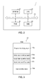
control section 11 mentioned above.FIG. 2 illustrates configuration of thecontrol section 11. - As illustrated in
FIG. 2 , thecontrol section 11 includes aCPU 31, read only memory (ROM) 32, random access memory (RAM) 33 (volatile memory), and EEPROM 34 (flash memory). The blocks listed above are connected to one another by abus 35. Internal configuration of theRAM 33 and theEEPROM 34 is explained further below. - The
ROM 32 stores data and a plurality of programs, such as firmware for performing various processing, in read-only form. TheRAM 33 is used as a work area by theCPU 31 and temporarily stores an operating system (OS), various applications that are being executed, and various types of data that are being processed. - The
EEPROM 34 is flash memory that is required to undergo initialization in block units prior to writing data thereto and that has an upper limit for the number of initializations. - The
CPU 31 controls each of the sections in accordance with a program stored in theROM 32 or thestorage section 21. - Through the above, configuration of the
control section 11 has been explained. - The following explains configuration of the
RAM 33.FIG. 3 illustrates an example of configuration of theRAM 33. - As illustrated in
FIG. 3 , theRAM 33 is partitioned into aprogram developing region 33p, actualdata recording regions log recording region 33d. Theprogram developing region 33p is used to develop a program executed by theCPU 31 and as working memory during execution of the program. The actualdata recording regions 33a to 33c store values for variables used by the program. Region partitioning of theRAM 33 may be performed theoretically or physically. The actualdata recording regions 33a to 33c are equivalent to a "first actual data region". Thelog recording region 33d is equivalent to a "first log region". - Although an actual data recording region is formed by three regions in the present explanation, such a configuration is only an example and the actual data recording region may be formed by any number of regions.
- For example, suppose a situation in which a variable name of a printing counter used to count the number of sheets printed by the
image forming apparatus 10 is denoted PCNT. The actualdata recording region 33a is used to store a value for PCNT. In a situation in which at the present point in time printing has for example been performed on 100 sheets, a value of "100" is stored in the actualdata recording region 33a. - When the
image forming apparatus 10 then for example performs printing on a further 2 sheets, the value for the printing counter PCNT in the actualdata recording region 33a is updated from "100" to "102". TheCPU 31 writes a piece of update information to thelog recording region 33d such as "PCNT, 102, 1". - The update information recorded in the
log recording region 33d includes update data that has been used in the aforementioned updating (i.e., "102" in the above example). The update information is formed by three items: a data ID, the update data, and a write count. The write count is a counter indicating the number of times that data updating has been performed since performance of refresh processing (explained further below). - In a situation in which a plurality of pieces of update information each having a data ID of "PCNT" are recorded in the
log recording region 33d, an up-to-date value for the variable PCNT can be determined by selecting a piece of update information including a largest value write count from among the plurality of pieces of update information. - In a situation in which, for example, the
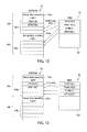
image forming apparatus 10 performs printing on a further 3 sheets, the value for the printing counter PCNT in the actualdata recording region 33a is updated from "102" to "105". In the above situation, an entry of "PCNT, 105, 2" is written to thelog recording region 33d as a next entry after the entry of "PCNT, 102, 1" in the first row (refer toFIG. 4 ). - Note that an entry in the third row in
FIG. 4 for example indicates that a value "OK" has been written as first update data for a variable STAT. The variable STAT is a variable that indicates the status of theimage forming apparatus 10 and is stored in the actualdata recording region 33c illustrated inFIG. 3 . - In order to simplify explanation, the above explains an example in which a value for one variable-print counter PCNT-is stored in one actual
data recording region 33a, but the above configuration is not a limitation and values for a plurality of variables may be stored in one actual data recording region. - Also, the electronic device according to the present invention is envisaged as being an embedded device or the like and thus it is preferable that a designer of the electronic device is aware of and determines in advance a name (data ID) of each variable, such as a counter, and also a data length and a memory address for storage thereof.
- The
program developing region 33p is not a key point of the present invention and thus explanation thereof is omitted below. - Through the above, configuration of the
RAM 33 has been explained. - The following explains configuration of the
EEPROM 34.FIG. 5 illustrates an example of configuration of theEEPROM 34. - In the example illustrated in
FIG. 5 , theEEPROM 34 includes threeblocks EEPROM 34, it is necessary to perform initialization in block units prior to writing the data. TheEEPROM 34 has an upper limit for the number of initializations. - The
block 34a is partitioned into an actualdata recording region 341a and alog recording region 342a. - The
block 34b is partitioned into an actualdata recording region 341b and alog recording region 342b. - The
block 34c is partitioned into an actualdata recording region 341c and alog recording region 342c. The actualdata recording region 341a, the actualdata recording region 341b, and the actualdata recording region 341c are each equivalent to a "second actual data region". Thelog recording region 342a, thelog recording region 342b, and thelog recording region 342c are each equivalent to a "second log region". - Partitioning of the
EEPROM 34 into the six regions explained above may be performed theoretically or physically. - Actual data corresponding to the contents of the actual
data recording region 33a is recorded in the actualdata recording region 341a. - Actual data corresponding to the contents of the actual
data recording region 33b is recorded in the actualdata recording region 341b. Actual data corresponding to the contents of the actualdata recording region 33c is recorded in the actualdata recording region 341c. - In other words, the actual
data recording region 33a, the actualdata recording region 33b, and the actualdata recording region 33c may respectively have the same capacity as the actualdata recording region 341a, the actualdata recording region 341b, and the actualdata recording region 341c. - Update information such as that illustrated in
FIG. 4 is recorded in thelog recording regions 342a to 342c. The method by which update information is recorded in thelog recording regions 342a to 342c is explained further below. - It should be noted that in a situation in which, for example, storage of the value for the printing counter PCNT is assigned to the actual
data recording region 33a illustrated inFIG. 3 , storage of the value for the printing counter PCNT is also assigned to the actualdata recording region 341a. On the other hand, update information for the printing counter PCNT is not necessarily recorded in thelog recording region 342a and update information for the variable STAT indicating the status of theimage forming apparatus 10 may be recorded in thelog recording region 342a. - Also, for a reason explained further below with reference to
FIG. 8 , preferably thelog recording regions 342a to 342c each have a greater capacity than thelog recording region 33d illustrated inFIG. 3 . - Through the above, configuration of the
EEPROM 34 has been explained. - The following explains the flow of data processing between the
EEPROM 34 and theRAM 33 during start-up of theimage forming apparatus 10.FIG. 6 illustrates data processing between theEEPROM 34 and theRAM 33 during start-up of theimage forming apparatus 10. - Prior to start-up of the
image forming apparatus 10, there is no data in theRAM 33 and all data (actual data and update information) is in theEEPROM 34. - For example, a value of "100" for the printing counter PCNT is recorded in the actual
data recording region 341a and a piece of update information "PCNT, 102, 1" for the printing counter PCNT is recorded in thelog recording region 342b. Also, a piece of update information "PCNT, 105, 2" for the printing counter PCNT is recorded in thelog recording region 342c. - Upon start-up of the
image forming apparatus 10, once theRAM 33 has been initialized, contents of the actualdata recording region 341a, the actualdata recording region 341b, and the actualdata recording region 341c are respectively copied to the actualdata recording region 33a, the actualdata recording region 33b, and the actualdata recording region 33c corresponding thereto. - Next, data in the actual
data recording regions log recording regions 342a to 342c. - Through the above processing, a state is reached in which up-to-date actual data is stored in the actual
data recording regions 33a to 33c of theRAM 33. - Through the above, the flow of data processing between the
EEPROM 34 and theRAM 33 during start-up of theimage forming apparatus 10 has been explained. - The following explains processing performed by the
CPU 31 for updating actual data in theRAM 33.FIG. 7 illustrates the processing performed by theCPU 31 for updating the actual data in theRAM 33. - For example, when the value for the printing counter PCNT in the actual
data recording region 33a is updated from "100" to "102", a piece of update information "PCNT, 102, 1" is written to thelog recording region 33d as explained above. - Thus, a piece of update information is additionally written to the
log recording region 33d each time update processing occurs for actual data in any of the actualdata recording regions 33a to 33c (processes A1 to A3 illustrated inFIG. 7 ). - Processing that accompanies updating of actual data is normally complete once updating has been performed with respect to the
RAM 33 and processing for writing to theEEPROM 34 is not normally performed. - As a result of not performing writing to the
EEPROM 34 every time that theRAM 33 is updated, the number of writes to theEEPROM 34 can be reduced and thus the lifetime of theEEPROM 34 can be extended. - Through the above, the flow of processing during updating of actual data in the
RAM 33 by theCPU 31 has been explained. - The following explains the flow of processing when data in the
RAM 33 is written to theEEPROM 34 at a specific timing.FIG. 8 illustrates the processing when the data in theRAM 33 is written to theEEPROM 34 at the specific timing. - Note that the aforementioned specific timing may for example be a periodic timing that is triggered by a timer, a timing at which a collective writing command is executed upon, for example, shutdown of the
image forming apparatus 10, a timing at which specific actual data is updated, or a timing at which there is no longer any free space in thelog recording region 33d. - At the specific timing, the
CPU 31 first collects pieces of update information in thelog recording region 33d of theRAM 33 and writes the collected update information to any one of thelog recording regions 342a to 342c of theEEPROM 34. The writing is performed in a form such that the collected update information is added to update information that is already recorded in thelog recording regions 342a to 342c. - The writing is performed by switching between blocks in order. In other words, supposing that writing is performed to the third block (
block 34c) at one instance of the specific timing, writing is performed to the first block (block 34a) at a next instance of the specific timing. - The order in which writing is performed to the blocks is preset. For example, update information may be written to the blocks by repeating a preset order of writing to the first block, followed by the second block, followed by the third block, and then starting again from the first block.
- Suppose that in the example illustrated in
FIG. 8 , writing has been performed to the third block at a previous instance of the specific timing. Thus, at the present instance of the specific timing, writing is performed to the first block (process A1 illustrated inFIG. 8 ). - In a situation in which free space of the log recording region of a given block is insufficient during writing of collected update information, a remaining portion of the collected update information is written to a block that is scheduled to be written to next.
- Once the writing is complete, the
CPU 31 erases the update information recorded in thelog recording region 33d (process A2 illustrated inFIG. 8 ). - A key point of the processing described above is that only the collected update data is written to only a specific block of the
EEPROM 34 without writing actual data to theEEPROM 34 from theRAM 33. - By adopting the configuration described above, the number of writes to the
EEPROM 34 can be reduced and writing can be performed evenly to the blocks of the EEPROM 34 (i.e., wear leveling can be performed). - Through the above, the processing when data in the
RAM 33 is written to theEEPROM 34 at the specific timing has been explained. - The following explains refresh processing.
FIG. 9 is provided in order to facilitate explanation of the refresh processing. - The refresh processing is processing that is performed when free space of the log recording region of a given block is insufficient at the specific timing described above and thus update information recorded in the
log recording region 33d cannot be copied to the log recording region that has insufficient free space. - In the refresh processing, actual data in each of the actual
data recording regions 341a to 341c of theEEPROM 34 is overwritten with actual data in the corresponding one of the actualdata recording regions 33a to 33c of the RAM 33 (process A1 illustrated inFIG. 9 ). - The actual data in the actual
data recording regions 33a to 33c of theRAM 33 is in an up-to-date state and thus as a result the processing described above, the actual data in the actualdata recording regions 341a to 341c is also in an up-to-date state. - Therefore, update information in the
log recording region 33d of theRAM 33 and update information in thelog recording regions 342a to 342c of theEEPROM 34 is erased (processes A2 and A3 illustrated inFIG. 9 ) as the update information is no longer required for updating the actual data to an up-to-date state. - The reason for performing the refresh processing is that if writing processing is for example performed at the specific timing described above in a situation in which the log recording regions of the first and second blocks have insufficient free space, writing is performed intensively to the third block and thus cannot be performed evenly.
- Through the above, the flow of processing during refreshing has been explained.
- The following explains an image forming apparatus 10a according to a second embodiment. The image forming apparatus 10a is an apparatus in which the
control section 11 of theimage forming apparatus 10 has been partially modified. - The following explains two points of modification and the modification methods thereof. Note that modification methods involve a partial change of the
control section 11 and do not involve any change to actual configuration of the image forming apparatus 10a or thecontrol section 11. Therefore, elements are referred to using the same reference signs as in the first embodiment and explanation of configuration is omitted. - First explanation is given of a first point of modification of the
image forming apparatus 10 according to the first embodiment and a modification method thereof. - Suppose for example that updating of data for the printing counter PCNT occurs regularly and that timing for writing to the
EEPROM 34 is considered to have been reached once six pieces of update information for the printing counter PCNT have accumulated in thelog recording region 33d of theRAM 33. - In such a situation, the
control section 11 of theimage forming apparatus 10 according to the first embodiment collects all pieces of update information in thelog recording region 33d and additionally writes the collected update information to a given log recording region of theEEPROM 34. In a situation such as illustrated for example inFIG. 10 in which the update information is too large to be additionally written to thelog recording region 342a of one block, it is necessary to also perform writing to thelog recording region 342b of the next block (processes A1 and A2 illustrated inFIG. 10 ). - In consideration of the above, in the
control section 11 of the image forming apparatus 10a according to the second embodiment, the data amount of collected update information that is to be written to theEEPROM 34 is reduced. - Namely, when the
control section 11 of the image forming apparatus 10a collects pieces of update information from thelog recording region 33d for writing to a given one of thelog recording regions 342a to 342c at the specific timing, thecontrol section 11 extracts only a most recent piece of update information for each data ID and collects the extracted pieces of update information. - In the example described above in which there are six pieces of update information for the printing counter PCNT, the
control section 11 only extracts a most recent piece of update information from among the six pieces of update information by referring to the write counts thereof (update count information) (process A1 illustrated inFIG. 11 ). Therefore, the amount of update information that is written to theEEPROM 34 can be reduced to one sixth in the example described above (refer toFIG. 11 ). - Through the above, the first point of modification of the
image forming apparatus 10 according to the first embodiment and the modification method thereof have been explained. - First explanation is given of a second point of modification of the
image forming apparatus 10 according to the first embodiment and a modification method thereof. - Suppose for example that each of the
log recording regions 342a to 342c in theEEPROM 34 has capacity for recording four pieces of update information as illustrated inFIG. 12 . Also suppose that at a present write timing, writing starts from thelog recording region 342a of the first block. Thelog recording region 342a already has update information recorded as two entries therein and thus only two entries are free for writing. - When additional writing of four pieces of update information from the
log recording region 33d of theRAM 33 is to be performed in the state described above, thelog recording region 342a has insufficient free space and thus some of the pieces of update information are additionally written to thelog recording region 342b of the second block. Therefore, the number of blocks to which writing is performed is increased to two in the above situation. - In consideration of the above, the
control section 11 of the image forming apparatus 10a according to the second embodiment does not simply additionally write update information in theRAM 33 to a given log recording region of theEEPROM 34, but also reads update information that is already recorded in the log recording region of theEEPROM 34 to which writing is to be performed. When a piece of update information to be written has the same data ID as a piece of recorded update information that is read, the update information having the same data ID is overwritten on the piece of update information that is already recorded. - Supposing the same situation as illustrated in
FIG. 12 , with respect to actual data of "STAT" and "PCNT" for each of which a piece of update information to be written has the same data ID (data identifier) as a piece of update information that is already recorded, the pieces of update information to be written are not additionally written, but are instead overwritten on the already recorded pieces of update information "PCNT, 98, 1" and "STAT, NG, 1" which are out-of-date. - Therefore, in the example illustrated in
FIG. 13 , the four pieces of update information in thelog recording region 33d of theRAM 33 can all be written to thelog recording region 342a of the first block. In other words, the number of blocks to which writing is performed can be reduced to one. - Through the above, the second point of modification of the
image forming apparatus 10 according to the first embodiment and the modification method thereof have been explained. - The present invention is of course not limited to the embodiments described above and various alterations may be performed so long as such alterations do not deviate from the intended scope of the present invention.
Claims (9)
- An electronic device (10) comprising:- a volatile memory (33) including- a first actual data region (33a, 33b; 33c) configured to record actual data therein, and- a first log region (33d) configured to record one or more pieces of update information therein, each including at least update data used for updating the actual data recorded in the first actual data region;- a flash memory (34) that includes a plurality of blocks and that is configured to undergo initialization in block units when either or both of the actual data and the update information are to be written thereto, each of the blocks including- a second actual data region (341a, 341b; 341c) configured to record at least a portion of the actual data therein, and- a second log region (342a, 342b; 342c) configured to record update information therein that is written from the first log region (33d); and- a CPU (31) configured to- write each of the pieces of update information to the first log region when updating the actual data in the first actual data region using update data corresponding to the piece of update information, and- at a preset specific timing, collect one or more of the pieces of update information recorded in the first log region (33d), write the pieces of update information that are collected to the second log regions (342a, 342b; 342c) in accordance with a specific order, and subsequently initialize the first log region (33d).
- The electronic device (10) according to claim 1, wherein
when the pieces of update information that are collected cannot be written to the second log region (342a, 342b; 342c) of a given one of the blocks due to the second log region (342a, 342b; 342c) having insufficient free space, the CPU (31):- overwrites the actual data recorded in the first actual data region (33a, 33b; 33c) on corresponding actual data recorded in the second actual data regions (341a, 341b; 341c); and- initializes the first log region (33d) and the second log regions (342a, 342b; 342c). - The electronic device (10) according to claim 1 or 2, wherein
at the specific timing, the CPU (31) extracts most recent update information, based on update count information, from among the one or more pieces of update information recorded in the first log region (33d), collects one or more pieces of update information that are extracted as the most recent update information, writes the pieces of update information that are collected to the second log regions (342a, 342b; 342c) in accordance with the specific order, and subsequently initializes the first log region (33d). - The electronic device (10) according to claim 3, wherein- each of the pieces of update information further includes a data identifier that identifies the actual data that is updated, and- when the CPU (31) writes the pieces of update information that are collected to the second log regions (342a, 342b; 342c) in accordance with the specific order, with respect to a piece of update information to be written that includes the same data identifier as a piece of update data already recorded in a given one of the second log regions (342a, 342b; 342c) to which writing is to be performed, the CPU (31) overwrites the piece of update information including the same data identifier on the piece of update information already recorded in the given one of the second log regions (342a, 342b; 342c).
- The electronic device (10) according to any one of claims 1 to 4, wherein the specific timing is at least one of a periodic timing triggered by a timer, a timing at which a collective writing command is executed during shutdown of the electronic device (10), a timing at which specific actual data is updated, and a timing at which the first log region (33d) no longer has free space.
- The electronic device (10) according to any one of claims 1 to 5, wherein the specific order involves repetition of a preset order.
- The electronic device (10) according to any one of claims 1 to 6, wherein- the electronic device (10) is an image forming apparatus ; and- the electronic device (10) further comprises an image forming section (15) configured to form an image on a recording medium.
- The electronic device (10) according to claim 7, wherein- the volatile memory (33) is RAM, and- the flash memory (34) is EEPROM.
- A Method of updating a flash memory (34) of an electronic device (10), the electronic device (10) comprising:a volatile memory (33) including- a first actual data region (33a, 33b; 33c) configured to record actual data therein, and- a first log region (33d) configured to record one or more pieces of update information therein, each including at least update data used for updating the actual data recorded in the first actual data region;- the flash memory (34) that includes a plurality of blocks and that is configured to undergo initialization in block units when either or both of the actual data and the update information are to be written thereto, each of the blocks including- a second actual data region (341a, 341b; 341c) configured to record at least a portion of the actual data therein, and- a second log region (342a, 342b; 342c) configured to record update information therein that is written from the first log region (33d); and- a CPU (31), wherein
the CPU (31) writes each of the pieces of update information to the first log region when updating the actual data in the first actual data region using update data corresponding to the piece of update information, and wherein
the CPU (31), at a preset specific timing, collects one or more of the pieces of update information recorded in the first log region (33d), writes the pieces of update information that are collected to the second log regions (342a, 342b; 342c) in accordance with a specific order, and subsequently initializes the first log region (33d).
Applications Claiming Priority (2)
| Application Number | Priority Date | Filing Date | Title |
|---|---|---|---|
| JP2014083642A JP6168660B2 (en) | 2014-04-15 | 2014-04-15 | Electronics |
| JP2014085093A JP6168661B2 (en) | 2014-04-17 | 2014-04-17 | Electronics |
Publications (1)
| Publication Number | Publication Date |
|---|---|
| EP2933721A1 true EP2933721A1 (en) | 2015-10-21 |
Family
ID=53275956
Family Applications (1)
| Application Number | Title | Priority Date | Filing Date |
|---|---|---|---|
| EP15163487.0A Withdrawn EP2933721A1 (en) | 2014-04-15 | 2015-04-14 | Electronic device and image forming apparatus |
Country Status (3)
| Country | Link |
|---|---|
| US (1) | US9684853B2 (en) |
| EP (1) | EP2933721A1 (en) |
| CN (1) | CN105007387B (en) |
Families Citing this family (4)
| Publication number | Priority date | Publication date | Assignee | Title |
|---|---|---|---|---|
| CN107239411B (en) * | 2017-06-06 | 2020-12-08 | 上汽通用汽车有限公司 | Memory management method and system for vehicle-mounted controller |
| CN109284177B (en) * | 2017-07-20 | 2021-03-30 | 北京京东尚科信息技术有限公司 | A data update method and device |
| TWI715371B (en) * | 2019-12-25 | 2021-01-01 | 新唐科技股份有限公司 | One-time programmable memory device and fault tolerant method thereof |
| TWI719779B (en) | 2019-12-26 | 2021-02-21 | 新唐科技股份有限公司 | One-time programmable memory device and fault tolerant method thereof |
Family Cites Families (9)
| Publication number | Priority date | Publication date | Assignee | Title |
|---|---|---|---|---|
| JP3826617B2 (en) | 1998-05-14 | 2006-09-27 | セイコーエプソン株式会社 | Patent application title: PRINTER HAVING NONVOLATILE MEMORY AND METHOD FOR CONTROLLING WRITE TO NONVOLATILE MEMORY IN THE PRINTER |
| EP0957447B1 (en) * | 1998-05-14 | 2007-10-31 | Seiko Epson Corporation | Control method of saving data from volatile to nonvolatile memory in a printer |
| US7342675B2 (en) * | 2002-10-28 | 2008-03-11 | Hewlett-Packard Development Company, L.P. | Systems and methods for improved operation and troubleshooting of a printing device |
| JP4433684B2 (en) * | 2003-03-24 | 2010-03-17 | 富士ゼロックス株式会社 | Job processing apparatus and data management method in the apparatus |
| US7554855B2 (en) * | 2006-12-20 | 2009-06-30 | Mosaid Technologies Incorporated | Hybrid solid-state memory system having volatile and non-volatile memory |
| US8301833B1 (en) * | 2007-06-01 | 2012-10-30 | Netlist, Inc. | Non-volatile memory module |
| US9128821B2 (en) * | 2008-10-10 | 2015-09-08 | Seagate Technology Llc | Data updating in non-volatile memory |
| US10133662B2 (en) * | 2012-06-29 | 2018-11-20 | Sandisk Technologies Llc | Systems, methods, and interfaces for managing persistent data of atomic storage operations |
| JP2015141575A (en) * | 2014-01-29 | 2015-08-03 | 京セラドキュメントソリューションズ株式会社 | Image formation device and control method |
-
2015
- 2015-04-07 US US14/680,914 patent/US9684853B2/en not_active Expired - Fee Related
- 2015-04-09 CN CN201510166185.8A patent/CN105007387B/en not_active Expired - Fee Related
- 2015-04-14 EP EP15163487.0A patent/EP2933721A1/en not_active Withdrawn
Non-Patent Citations (3)
| Title |
|---|
| CHIN-HSIEN WU ET AL: "The Design of efficient initialization and crash recovery for log-based file systems over flash memory", ACM TRANSACTIONS ON STORAGE, vol. 2, no. 4, 1 November 2006 (2006-11-01), pages 449 - 467, XP055060437, ISSN: 1553-3077, DOI: 10.1145/1210596.1210600 * |
| GAL E ET AL: "ALGORITHMS AND DATA STRUCTURES FOR FLASH MEMORIES", ACM COMPUTING SURVEYS, ACM, NEW YORK, NY, US, US, vol. 37, no. 2, 1 June 2005 (2005-06-01), pages 138 - 163, XP002453935, ISSN: 0360-0300, DOI: 10.1145/1089733.1089735 * |
| WU M ET AL: "ENVY: A NON-VOLATILE, MAIN MEMORY STORAGE SYSTEM", PRINCIPLES OF PROGRAMMING LANGUAGES, ACM, 2 PENN PLAZA, SUITE 701 NEW YORK NY 10121-0701 USA, vol. 29, no. 11, 1 November 1994 (1994-11-01), pages 86 - 97, XP000491727, ISSN: 0362-1340, DOI: 10.1145/195470.195506 * |
Also Published As
| Publication number | Publication date |
|---|---|
| US20150294196A1 (en) | 2015-10-15 |
| US9684853B2 (en) | 2017-06-20 |
| CN105007387B (en) | 2018-04-06 |
| CN105007387A (en) | 2015-10-28 |
Similar Documents
| Publication | Publication Date | Title |
|---|---|---|
| JP5982025B1 (en) | Information processing apparatus and memory management program | |
| US8595745B2 (en) | Job-process swapping between multiple storage devices based on the most recently executed type of a process and historical execution count among plural types of processes | |
| EP2879051A1 (en) | An electronic device including a MTD used temporarily during non-volatile memory file system update | |
| US9684853B2 (en) | Image forming apparatus that writes data from volatile memory to non-volatile memory | |
| JP6004923B2 (en) | Information processing apparatus, control method therefor, and program | |
| JP6405736B2 (en) | Image processing apparatus, writing control program, and writing control method | |
| KR101339869B1 (en) | Image forming apparatus and method of overwriting for storage unit in image forming apparatus | |
| JP5658574B2 (en) | Image forming apparatus, control method therefor, and program | |
| KR20110057037A (en) | Display device and control method of display device | |
| JP6418400B2 (en) | Electronic equipment and information processing program | |
| JP6579324B2 (en) | Image forming apparatus and data processing program | |
| US20150213338A1 (en) | Image forming apparatus that performs writing into a non-volatile memory, and a method | |
| JP6083416B2 (en) | Job execution device, program, and data deletion method | |
| JP6410055B2 (en) | Image forming apparatus and data processing program | |
| JP2011165080A (en) | Electronic apparatus | |
| JP6168661B2 (en) | Electronics | |
| JP6168660B2 (en) | Electronics | |
| JP6124836B2 (en) | Electronic device and memory management method | |
| US20170177376A1 (en) | Electronic apparatus | |
| JP2007053735A (en) | Image forming apparatus and image data storage area replacement method | |
| US10956090B2 (en) | Memory system and electronic apparatus | |
| US10437488B2 (en) | Electronic device and non-transitory computer readable storage medium | |
| JP5976729B2 (en) | Electronics | |
| JP2008284711A (en) | Image forming apparatus | |
| JP6323393B2 (en) | Image forming apparatus |
Legal Events
| Date | Code | Title | Description |
|---|---|---|---|
| PUAI | Public reference made under article 153(3) epc to a published international application that has entered the european phase |
Free format text: ORIGINAL CODE: 0009012 |
|
| AK | Designated contracting states |
Kind code of ref document: A1 Designated state(s): AL AT BE BG CH CY CZ DE DK EE ES FI FR GB GR HR HU IE IS IT LI LT LU LV MC MK MT NL NO PL PT RO RS SE SI SK SM TR |
|
| AX | Request for extension of the european patent |
Extension state: BA ME |
|
| 17P | Request for examination filed |
Effective date: 20160415 |
|
| RBV | Designated contracting states (corrected) |
Designated state(s): AL AT BE BG CH CY CZ DE DK EE ES FI FR GB GR HR HU IE IS IT LI LT LU LV MC MK MT NL NO PL PT RO RS SE SI SK SM TR |
|
| STAA | Information on the status of an ep patent application or granted ep patent |
Free format text: STATUS: EXAMINATION IS IN PROGRESS |
|
| 17Q | First examination report despatched |
Effective date: 20180903 |
|
| RIC1 | Information provided on ipc code assigned before grant |
Ipc: G06F 12/02 20060101ALI20210705BHEP Ipc: G06F 16/174 20190101ALI20210705BHEP Ipc: G06F 8/654 20180101AFI20210705BHEP |
|
| GRAP | Despatch of communication of intention to grant a patent |
Free format text: ORIGINAL CODE: EPIDOSNIGR1 |
|
| STAA | Information on the status of an ep patent application or granted ep patent |
Free format text: STATUS: GRANT OF PATENT IS INTENDED |
|
| INTG | Intention to grant announced |
Effective date: 20210824 |
|
| STAA | Information on the status of an ep patent application or granted ep patent |
Free format text: STATUS: THE APPLICATION IS DEEMED TO BE WITHDRAWN |
|
| 18D | Application deemed to be withdrawn |
Effective date: 20220104 |