EP2933719A1 - A digital method and device for generating true random numbers - Google Patents
A digital method and device for generating true random numbers Download PDFInfo
- Publication number
- EP2933719A1 EP2933719A1 EP14165296.6A EP14165296A EP2933719A1 EP 2933719 A1 EP2933719 A1 EP 2933719A1 EP 14165296 A EP14165296 A EP 14165296A EP 2933719 A1 EP2933719 A1 EP 2933719A1
- Authority
- EP
- European Patent Office
- Prior art keywords
- signal
- sampling
- circuit
- ring
- cells
- Prior art date
- Legal status (The legal status is an assumption and is not a legal conclusion. Google has not performed a legal analysis and makes no representation as to the accuracy of the status listed.)
- Granted
Links
Images

Classifications
-
- G—PHYSICS
- G06—COMPUTING; CALCULATING OR COUNTING
- G06F—ELECTRIC DIGITAL DATA PROCESSING
- G06F7/00—Methods or arrangements for processing data by operating upon the order or content of the data handled
- G06F7/58—Random or pseudo-random number generators
- G06F7/588—Random number generators, i.e. based on natural stochastic processes
Definitions
- the present invention relates to a method and device for generating random numbers.
- Random numbers generation is implemented in various devices, such as cryptographic systems, smartcards authentication devices, electronic gaming devices, audio/video scrambling devices.
- Random number generation is critical to cryptographic systems.
- Symmetric cryptography such as Data Encryption Standard (DES) requires randomly selected encryption keys.
- Asymmetrical cryptography such as RSA, Diffie-Hellman and DSA requires randomly generated key pairs.
- SSL Secure Socket Layer
- a random number generator Because of the widespread use of random numbers in cryptography, a random number generator must be robust enough so that even if the design of the random number generator is known, a random number generated by the random number generator cannot be predicted.
- a class of random number generators called “pseudo-random number generators", use a deterministic process, i.e. having a predictable output, to generate a number from a seed. Such a random number generator can be easily compromised, particularly if the seed of the pseudo random number generator can be determined.
- true number random generators use a non-deterministic source, such as a noise source, e.g. a thermal or flicker noise source.
- a non-deterministic source such as a noise source, e.g. a thermal or flicker noise source.
- the random number generators using such a non-deterministic source comprise analog circuitry that makes random number generators complex to design and to integrate into the high-density integrated circuits of today.
- Other true random number generators use a low-frequency clocked circuit to sample the output of a Linear Feedback Shift Register (LFSR), the LFSR being driven by a higher frequency Free-Running ring Oscillator (FRO) with a random variation in the frequency to generate random numbers. Due to the sampling by a low frequency of a higher frequency oscillator, a predictable pattern may induce a failure of the oscillator, which is difficult to detect and prevent.
- LFSR Linear Feedback Shift Register
- FRO Free-Running ring Oscillator
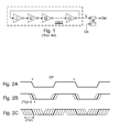
- the random number generator comprises a free-running ring oscillator OSC1 and a D-type flip-flop FF sampling an output signal S of the oscillator OSC1 at a rate defined by the frequency of a clock signal Clk.
- the oscillator OSC1 comprises an odd number of inverters I1, 12, 13, Im.
- the sampling flip-flop FF produces single-bit samples Out that are expected to be not predictable by an external observer.
- the period of the clock signal Clk is several orders of magnitude longer than the average oscillation period of the oscillator OSC1.
- the sampling clock is faster but only one every N samples is used whereas the other samples are discarded.
- FIGS. 2A, 2B, 2C represent waveforms of the signal S provided by the oscillator OSC1.
- Figure 2A represents a waveform produced by a noiseless oscillator or at the start of the oscillator OSC1.
- FIG 2B after p periods CP of the signal S, a small amount of jitter JT(p) appears in the signal S. Due to the cyclic structure of the oscillator OSC1, the jitter builds up within the oscillator.
- the probability function for the location (phase error) of an edge of the signal S after a given amount of time has a normal distribution centered around the 'ideal' edge, with a certain standard deviation that grows with time.
- the amount of jitter built up after a certain time from the start of the oscillator can be expressed as a probability density function that increases over time.
- the standard deviation of the probability density function modeling the probability of finding a given state oscillator change at a certain offset from the ideal output waveform increases with time.
- the jitter JT(n) accumulated in the signal S reaches half the period CP.
- the standard deviation of the phase error probability reaches at least half the oscillator period CP.
- the value of signal S can be 0 or 1 at any time.
- signal S has a value of 0 or 1 with a probability of 1/2.
- the time n ⁇ CP corresponds to the time needed for the accumulated jitter to cover the propagation time of the signal in the whole ring, i.e. the oscillator period.
- the jitter built-up between samples generates entropy in the sampled value (0 or 1) which can reach a maximum value of 1 bit (probability of 1/2 for either value 0 or 1). This uncertainty towards the sampled value determines the amount of entropy in the sample.
- the maximum entropy value of 1/2 can be reached when the sampling period is greater than n periods CP of the oscillator OSC1 ( figure 2C ). It results that the entropy bit rate produced by the random number generator of Figure 1 is low with respect to the frequency of the oscillator OSC1. Obviously, this bit rate can be increased by increasing the oscillation frequency of the oscillator OSC1. This is possible in a ring oscillator only by reducing the number of inverters. However a minimum number of inverters is required to ensure oscillation stability and protect the circuit against heating and electromigration effects.
- the entropy bit rate can also be increased by using several ring oscillators is parallel. However this solution increases the power consumption and the size of the random number generation circuit.
- a method for generating random numbers may include steps of: connecting signal transmitting cells to form a ring of cells connected in series, the cells comprising an odd number of inverters; simultaneously taking signal samples of signals transiting respectively between pairs of adjacent cells in the ring; and combining the signal samples to provide a random number.
- the signal samples are combined to determine a currently switching cell in the ring at a sampling time, the random number being determined as a function of the signal sample taken from an input or an output of the currently switching cell.
- the signal samples are combined to determine a parity bit of a binary word formed by the signal samples, the random number being determined as a function of the parity bit.
- a signal propagating in the ring accumulates jitter, a signal sampling being performed after the accumulated jitter covers a signal propagation time across a single one of the cells, and before the accumulated jitter covers half a period of an oscillator comprising the cell ring.
- the signal samples are taken periodically with a signal sampling period set to a value within an interval between once and twice the time for the jitter to cover the signal propagation time across a single one of the cells.
- a signal propagating in the ring accumulates jitter, a signal sampling being performed when the accumulated jitter covers a signal propagation time across all the cells.
- the signal samples are combined to determine an encoded value of a number of a currently switching cell in the ring, the random number being determined as a function of the encoded value.
- the signal samples are taken at each sampling period of a sampling clock signal and combined to provide a random number at every sampling period.
- Embodiments of the present disclosure also relate to a circuit for generating a random number, comprising: a ring of signal transmitting cells connected in series, the cells comprising an odd number of inverters; a sampling circuit configured to take simultaneously signal samples of signals transiting between pairs of adjacent cells in the ring; and a combinatorial circuit for combining the signal samples to produce a random number.
- the sampling circuit is clocked by a sampling clock signal to provide signal samples at each sampling period of the sampling clock signal.
- the combinatorial circuit is configured to combine the signal samples to determine a signal value output by a currently switching cell in the ring, and to determine the random number as a function of the signal value.
- the combinatorial circuit is configured to combine the signal samples to determine an encoded value of a number of a currently switching cell in the ring, and to determine the random number as a function of the encoded value.
- each of the cells comprises a delay line and/or an inverter, or the cell ring forms a Fibonacci or Galois oscillator.
- the sampling circuit comprises sampling units each having an input connected to an input or an output of one of the cells, and an output providing a signal sample at a sampling rate defined by a sampling clock signal.
- the sampling circuit comprises one sampling unit for each cell, the sampling unit having an input connected to an input or an output of the cell.
- the combinatorial circuit comprises XOR gates combining all the signal samples into a single bit.
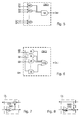
- FIG 3 provides a block diagram of a random number generator circuit RGC, according to an embodiment.
- the circuit RGC comprises a free-running oscillator OSC, a sampling circuit SPC, and a combinatorial circuit CBC.
- the oscillator OSC may be a ring oscillator such as the oscillator OSC of Figure 1 .
- the sampling circuit SPC is configured to sample signals within the oscillator OSC at a sampling rate defined by a sampling clock signal Clk.
- the combinatorial circuit CBC is configured to receive signal samples provided by the sampling circuit SPC and to combine them to provide random binary numbers.
- the oscillator OSC comprises m cells CL1, CL2, ... CLm, I1 connected in series so as to form a ring, where an output of a last one I1 of the cells is connected to an input of a first one CL1 of the cells.
- the cells CL1-CLm, I1 includes an odd number of inverters (m being an integer number), to make the signal propagating in the ring oscillate.
- the sampling circuit SPC comprises one sampling unit F0, F1, F2, F3 ... Fm, for each link connecting two adjacent cells CL1-CLm, I1 in the oscillator OSC.
- Each sampling unit F0-Fm comprises an input connected to the input (or output) of a respective one of the cells CL1-CLm.
- Each sampling unit F0-Fm provides a sample signal S0, S1, S2, S3, ... Sm to the combinatorial circuit CBC at each sampling period of the sampling clock signal Clk.
- Each of the sampling units F0-Fm comprises for example a D-type flip-flop receiving the signal to be sampled by an input D, and the clock signal Clk by a clock input, and providing the sampled signal by a direct output Q.
- the sampling period may be chosen to be greater than or equal to the time needed for the accumulated jitter to cover the propagation time in the ring, of a signal state change between two consecutive inputs of sampling units F0-Fm in the cell ring. If the signal is sampled in the ring between each cell CL1-CLm, I1, the sampling period has to be chosen greater than the time needed for the accumulated jitter to cover the propagation time of the signal in only one cell. In contrast, in the random number generator shown in Figure 1 , the sampling period has to be greater than the time needed for the accumulated jitter to cover the propagation time of the signal in the whole ring, i.e. the ring oscillator period.
- the oscillation period of the ring oscillator is equal to n ⁇ d. Because the jitter grows as a function of the square root of time, the sampling period of the circuit RGC ( figure 3 ) may be reduced by a factor n 2 with respect to the sampling period of the circuit of Figure 1 .
- the sampling circuit SPC may comprise less than one sampling unit F0-Fm per link between adjacent cells CL1-CLm, I1, e.g. one sampling unit for two or three of these links, but at least two sampling units.
- the clock signal Clk may have an accurate frequency or not.
- the clock signal Clk may be provided by another ring oscillator accumulating jitter, such as a free-running oscillator, to introduce another degree of randomness in the circuit. In this manner, the sampling period may be reduced without affecting the entropy of the random numbers provided.
- Each sampling unit F0-Fm may comprise another D-type flip-flop receiving the sample signals S0-Sm and clocked by a clock signal of the combinatorial circuit CBC.
- the circuit CBC receives the sample signals and provides a signal Out at a same frequency.
- the sampling period may be chosen to be greater than the time for the jitter to cover the propagation time of a signal state change across a single one of the cells CL1-CLm, I1.
- the sampling period may be set to a value within the interval between once and twice the time for the jitter to cover the propagation time of a signal state change across a single one of the cells CL1-CLm, I1, i.e. the time for the jitter to cover the time between the detection of a state change of the signal in input of one of the cells CL1-CLm, I1, and the detection of a state change in the signal output by the cell.
- the entropy of the signal Out is based on the unpredictability of the state of the cell which is currently switching, after a given time, or the unpredictability of which one of two adjacent cells is currently switching.
- FIG. 4 is a block diagram of an example of the combinatorial logic circuit CBC.
- the combinatorial circuit CBC comprises XOR gates X1 combining the signal samples from the sampling units F0-Fm, and one output providing a binary signal Out. If the number of sample signals S0-Sm to high level (1) is odd, then the signal Out is set to high level (1). Conversely, if the number of sample signals S0-Sm to high level (0) is even, then the signal Out is set to low level (0). In other words, the circuit CBC sets the signal Out to the parity value of the binary word formed by the sample signals S0-Sm.
- Figure 5 represents another implementation of the combinatorial circuit that can be used when each of the cells CL1-Clm is an inverter.
- the combinatorial circuit CBC1 of Figure 5 comprises an XOR gate X11 combining the input and output signals of each cell (numbered from 0) having an odd rank in the ring, and a NAND gate NG combining the outputs of the XOR gates X11.
- the gate NG provides the signal Out at a state depending on the rank, odd or even, of the switching cell at the sampling time of the received signal samples.
- the combinatorial circuit CBC is configured to detect which one of the cells CL1-CLm, I1 is currently about to switch at the sampling time of the signal samples provided to the circuit CBC.
- the circuit CBC may be configured to output the input (or output) value of the detected currently switching cell.
- Figure 6 represents another implementation of the combinatorial circuit that can be used when each of the cells CL1-Clm is an inverter.
- the combinatorial circuit CBC2 of Figure 6 comprises an AND gate A1 combining the input and output signals of each cell in the ring, and an OR gate OG combining the outputs of the gates A1.
- the gate OG provides the signal Out at a state of the output signal of the switching cell at the sampling time of the received signal samples.
- the combinatorial circuit CBC is configured to compare the sample signals S0-Sm provided at each clock signal Clk occurrence by the sampling circuit SPC, and to detect on the basis of this comparison, which of the cells CL1-CLm, I1 is currently switching.
- the output value Out of the combinatorial circuit CBC may then be an encoded value of the number of the detected currently switching cell.
- the sampling period may be chosen to be greater than the time for the jitter to cover the propagation time of a signal state change across all the cells CL1-CLm, I1. Thus the sampling period may be chosen greater than the time for the jitter to cover half the oscillator period.
- the sampling period may be set to a value within the interval between once and twice the time for the jitter to cover half the oscillator period.
- the entropy of the signal Out is based on the unpredictability of the actual transition location in the ring oscillator OSC after given time.
- the encoded value of the number of the currently switching cell may comprise a number of bits depending on the number m+1 of cells CL1-CLm or sampling units F0-Fm.
- each of the cells CL1-CLm is a delay line
- the cell I1 is an inverter.
- Each delay line CL1-CLm may comprise an even number of inverters.
- a delay line which is currently switching can be detected by comparing the input signal with the output signal of the delay line, as sampled by the sampling circuit SPC.
- the delay line having an input signal different from its output signal is currently switching.
- the inverter I1 it is currently switching if its input signal is the same as its output signal, as sampled by the sampling circuit SPC.
- each of the cells CL1-CLm is an inverter, the number of inverters connected within the ring of the oscillator OSC being odd.
- the oscillator OSC is a chaotic oscillator such as a Fibonacci ring oscillator or a Galois ring oscillator.
- Figure 7 represents one cell CL of the cells CL1-CLm of a Fibonacci oscillator.
- Each cell CL comprises an inverter IN1, a switch SW1 and an OR gate OG1.
- the oscillator comprises an odd number of inverters I1, IN1.
- An input of the inverter IN1 is connected to an input of the cell CL.
- An output of the inverter IN1 is connected to an output of the cell CL and is linked to an input of the gate OG1 by means of the switch SW1.
- the gate OG1 is interposed in the return link from the inverter I1 to the first cell CL1 of the ring oscillator, i.e. an input of the gate OG1 is connected to an output of the gate OG1 of an adjacent cell CL1-CLm or to an output of the inverter I1, and an output of the gate OG1 is connected to an input of the gate OG1 of an adjacent cell CL1-CLm or to the input of the inverter IN1 of the first cell CL1.
- the oscillator OSC is a Galois ring oscillator.
- Figure 8 represents one cell CL' of the cells CL1-CLm of such an oscillator.
- Each cell CL1-CLm comprises an inverter IN2, a switch SW2 and an OR gate OG2.
- the oscillator comprises an odd number of inverters I1, IN2.
- An input of the inverter IN2 is connected to an input of the cell CL'.
- An output of the inverter IN2 is connected to an input of the gate OG2.
- An output of the gate OG2 is connected to an output of the cell CL'.
- the return link connecting the output of the last cell (inverter I1) to the input of the first cell CL1 of the ring oscillator is linked to an input of the gate OG2 by means of the switch SW2.
- the methods disclosed herein may be implemented by software programs executable by a computer system. Further, implementations may include distributed processing and parallel processing.
- the disclosed random number generator circuit may be used to generate only one number before it is turned off. Thus it is not necessary to provide a clock signal to the sampling units F0-Fm.
- Many other signal sampling circuits are known such as JK- or T-type flip-flops or latches. Thus one of these circuits may be chosen for the sampling units instead of a D-type flip-flop.
Abstract
Description
- The present invention relates to a method and device for generating random numbers.
- Random numbers generation is implemented in various devices, such as cryptographic systems, smartcards authentication devices, electronic gaming devices, audio/video scrambling devices.
- Random number generation is critical to cryptographic systems. Symmetric cryptography such as Data Encryption Standard (DES) requires randomly selected encryption keys. Asymmetrical cryptography such as RSA, Diffie-Hellman and DSA requires randomly generated key pairs. Furthermore, some cryptographic protocols such as SSL (Secure Socket Layer) use random challenges in authentication processes.
- Because of the widespread use of random numbers in cryptography, a random number generator must be robust enough so that even if the design of the random number generator is known, a random number generated by the random number generator cannot be predicted. A class of random number generators, called "pseudo-random number generators", use a deterministic process, i.e. having a predictable output, to generate a number from a seed. Such a random number generator can be easily compromised, particularly if the seed of the pseudo random number generator can be determined.
- In contrast, true number random generators use a non-deterministic source, such as a noise source, e.g. a thermal or flicker noise source. However, the random number generators using such a non-deterministic source comprise analog circuitry that makes random number generators complex to design and to integrate into the high-density integrated circuits of today. Other true random number generators use a low-frequency clocked circuit to sample the output of a Linear Feedback Shift Register (LFSR), the LFSR being driven by a higher frequency Free-Running ring Oscillator (FRO) with a random variation in the frequency to generate random numbers. Due to the sampling by a low frequency of a higher frequency oscillator, a predictable pattern may induce a failure of the oscillator, which is difficult to detect and prevent.
- Another true random number generator is shown in
Figure 1 . The random number generator comprises a free-running ring oscillator OSC1 and a D-type flip-flop FF sampling an output signal S of the oscillator OSC1 at a rate defined by the frequency of a clock signal Clk. The oscillator OSC1 comprises an odd number of inverters I1, 12, 13, Im. The sampling flip-flop FF produces single-bit samples Out that are expected to be not predictable by an external observer. Typically, the period of the clock signal Clk is several orders of magnitude longer than the average oscillation period of the oscillator OSC1. In an alternative implementation, the sampling clock is faster but only one every N samples is used whereas the other samples are discarded. - Internal noise sources in the elements forming the oscillator OSC1 influence switching times of the inverters I1-Im, and thus the output frequency of the oscillator OSC1 builds up a certain amount of jitter or phase noise over time, compared to a noiseless oscillator.
Figures 2A, 2B, 2C represent waveforms of the signal S provided by the oscillator OSC1.Figure 2A represents a waveform produced by a noiseless oscillator or at the start of the oscillator OSC1. Infigure 2B , after p periods CP of the signal S, a small amount of jitter JT(p) appears in the signal S. Due to the cyclic structure of the oscillator OSC1, the jitter builds up within the oscillator. The probability function for the location (phase error) of an edge of the signal S after a given amount of time has a normal distribution centered around the 'ideal' edge, with a certain standard deviation that grows with time. The amount of jitter built up after a certain time from the start of the oscillator can be expressed as a probability density function that increases over time. In other words, the standard deviation of the probability density function modeling the probability of finding a given state oscillator change at a certain offset from the ideal output waveform increases with time. Infigure 2C , after n periods CP, the jitter JT(n) accumulated in the signal S reaches half the period CP. At this time, the standard deviation of the phase error probability reaches at least half the oscillator period CP. In this latter case, the value of signal S can be 0 or 1 at any time. Thus signal S has a value of 0 or 1 with a probability of 1/2. The time n·CP corresponds to the time needed for the accumulated jitter to cover the propagation time of the signal in the whole ring, i.e. the oscillator period. - Most of the noise sources acting on the inverters of the oscillator OSC1 to generate jitter are attributed to external causes, such as temperature variations, supply voltage variations, signal crosstalk, etc. Because most of the noise sources are due to external influences on the circuit, their contribution at a given time during operation of the oscillator OSC1 can not be estimated. Thus it is difficult or even impossible to estimate an amount of the jitter that can be accumulated in the circuit, which is necessary to determine the minimum sample period. However it is possible to estimate a lower bound for the amount of jitter that will occur. It has been determined that the standard deviation of the accumulated jitter grows proportionally with the square root of time (see "Phase Noise and Jitter in CMOS Ring Oscillators", Asad A. Abidi, IEEE Journal of Solid-State Circuits, Vol. 41, No. 8, August 2006).
- If the sampling period is long enough, the jitter built-up between samples generates entropy in the sampled value (0 or 1) which can reach a maximum value of 1 bit (probability of 1/2 for either value 0 or 1). This uncertainty towards the sampled value determines the amount of entropy in the sample. In a ring oscillator such as the oscillator OSC1, the maximum entropy value of 1/2 can be reached when the sampling period is greater than n periods CP of the oscillator OSC1 (
figure 2C ). It results that the entropy bit rate produced by the random number generator ofFigure 1 is low with respect to the frequency of the oscillator OSC1. Obviously, this bit rate can be increased by increasing the oscillation frequency of the oscillator OSC1. This is possible in a ring oscillator only by reducing the number of inverters. However a minimum number of inverters is required to ensure oscillation stability and protect the circuit against heating and electromigration effects. - The entropy bit rate can also be increased by using several ring oscillators is parallel. However this solution increases the power consumption and the size of the random number generation circuit.
- It is therefore desirable to produce random samples with an increased sampling rate while maintaining or improving the entropy of each sample. It is also desirable to design a random number generator circuit having a low power consumption and a reduced size.
- A method is described for generating random numbers. This method may include steps of: connecting signal transmitting cells to form a ring of cells connected in series, the cells comprising an odd number of inverters; simultaneously taking signal samples of signals transiting respectively between pairs of adjacent cells in the ring; and combining the signal samples to provide a random number.
- According to an embodiment, the signal samples are combined to determine a currently switching cell in the ring at a sampling time, the random number being determined as a function of the signal sample taken from an input or an output of the currently switching cell.
- According to an embodiment, the signal samples are combined to determine a parity bit of a binary word formed by the signal samples, the random number being determined as a function of the parity bit.
- According to an embodiment, a signal propagating in the ring accumulates jitter, a signal sampling being performed after the accumulated jitter covers a signal propagation time across a single one of the cells, and before the accumulated jitter covers half a period of an oscillator comprising the cell ring.
- According to an embodiment, the signal samples are taken periodically with a signal sampling period set to a value within an interval between once and twice the time for the jitter to cover the signal propagation time across a single one of the cells.
- According to an embodiment, a signal propagating in the ring accumulates jitter, a signal sampling being performed when the accumulated jitter covers a signal propagation time across all the cells.
- According to an embodiment, the signal samples are combined to determine an encoded value of a number of a currently switching cell in the ring, the random number being determined as a function of the encoded value.
- According to an embodiment, the signal samples are taken at each sampling period of a sampling clock signal and combined to provide a random number at every sampling period.
- Embodiments of the present disclosure also relate to a circuit for generating a random number, comprising: a ring of signal transmitting cells connected in series, the cells comprising an odd number of inverters; a sampling circuit configured to take simultaneously signal samples of signals transiting between pairs of adjacent cells in the ring; and a combinatorial circuit for combining the signal samples to produce a random number.
- According to an embodiment, the sampling circuit is clocked by a sampling clock signal to provide signal samples at each sampling period of the sampling clock signal.
- According to an embodiment, the combinatorial circuit is configured to combine the signal samples to determine a signal value output by a currently switching cell in the ring, and to determine the random number as a function of the signal value.
- According to an embodiment, the combinatorial circuit is configured to combine the signal samples to determine an encoded value of a number of a currently switching cell in the ring, and to determine the random number as a function of the encoded value.
- According to an embodiment, each of the cells comprises a delay line and/or an inverter, or the cell ring forms a Fibonacci or Galois oscillator.
- According to an embodiment, the sampling circuit comprises sampling units each having an input connected to an input or an output of one of the cells, and an output providing a signal sample at a sampling rate defined by a sampling clock signal.
- According to an embodiment, the sampling circuit comprises one sampling unit for each cell, the sampling unit having an input connected to an input or an output of the cell.
- According to an embodiment, the combinatorial circuit comprises XOR gates combining all the signal samples into a single bit.
- The method and/or device may be better understood with reference to the following drawings and description. Non-limiting and non-exhaustive descriptions are described with the following drawings. In the figures, like referenced signs may refer to like parts throughout the different figures unless otherwise specified.
-
Figure 1 previously described is a block diagram of a conventional true random number generator circuit comprising a ring oscillator; -
Figure 2 previously described shows waveforms of an output signal of the ring oscillator ofFigure 1 ; -
Figure 3 is a block diagram of a true random number generator circuit, according to an embodiment; -
Figure 4 is a block diagram of a combinatorial logic circuit of the circuit shown inFigure 3 , according to an embodiment; -
Figure 5 is a block diagram of a combinatorial logic circuit of the circuit shown inFigure 3 , according to another embodiment; -
Figure 6 is a block diagram of a combinatorial logic circuit of the circuit shown inFigure 3 , according to another embodiment; -
Figure 7 is a block diagram of a cell circuit of the ring oscillator, according to another embodiment; -
Figure 8 is a block diagram of a cell circuit of the ring oscillator, according to another embodiment. -
Figure 3 provides a block diagram of a random number generator circuit RGC, according to an embodiment. The circuit RGC comprises a free-running oscillator OSC, a sampling circuit SPC, and a combinatorial circuit CBC. The oscillator OSC may be a ring oscillator such as the oscillator OSC ofFigure 1 . The sampling circuit SPC is configured to sample signals within the oscillator OSC at a sampling rate defined by a sampling clock signal Clk. The combinatorial circuit CBC is configured to receive signal samples provided by the sampling circuit SPC and to combine them to provide random binary numbers. - In the example of
Figure 3 , the oscillator OSC comprises m cells CL1, CL2, ... CLm, I1 connected in series so as to form a ring, where an output of a last one I1 of the cells is connected to an input of a first one CL1 of the cells. The cells CL1-CLm, I1 includes an odd number of inverters (m being an integer number), to make the signal propagating in the ring oscillate. The sampling circuit SPC comprises one sampling unit F0, F1, F2, F3 ... Fm, for each link connecting two adjacent cells CL1-CLm, I1 in the oscillator OSC. Each sampling unit F0-Fm comprises an input connected to the input (or output) of a respective one of the cells CL1-CLm. Each sampling unit F0-Fm provides a sample signal S0, S1, S2, S3, ... Sm to the combinatorial circuit CBC at each sampling period of the sampling clock signal Clk. Each of the sampling units F0-Fm comprises for example a D-type flip-flop receiving the signal to be sampled by an input D, and the clock signal Clk by a clock input, and providing the sampled signal by a direct output Q. - It results that the sampling period may be chosen to be greater than or equal to the time needed for the accumulated jitter to cover the propagation time in the ring, of a signal state change between two consecutive inputs of sampling units F0-Fm in the cell ring. If the signal is sampled in the ring between each cell CL1-CLm, I1, the sampling period has to be chosen greater than the time needed for the accumulated jitter to cover the propagation time of the signal in only one cell. In contrast, in the random number generator shown in
Figure 1 , the sampling period has to be greater than the time needed for the accumulated jitter to cover the propagation time of the signal in the whole ring, i.e. the ring oscillator period. Thus if d is the propagation time of the signal in a single cell, and n the number of cells, the oscillation period of the ring oscillator is equal to n·d. Because the jitter grows as a function of the square root of time, the sampling period of the circuit RGC (figure 3 ) may be reduced by a factor n2 with respect to the sampling period of the circuit ofFigure 1 . - The sampling circuit SPC may comprise less than one sampling unit F0-Fm per link between adjacent cells CL1-CLm, I1, e.g. one sampling unit for two or three of these links, but at least two sampling units.
- The clock signal Clk may have an accurate frequency or not. The clock signal Clk may be provided by another ring oscillator accumulating jitter, such as a free-running oscillator, to introduce another degree of randomness in the circuit. In this manner, the sampling period may be reduced without affecting the entropy of the random numbers provided. Each sampling unit F0-Fm may comprise another D-type flip-flop receiving the sample signals S0-Sm and clocked by a clock signal of the combinatorial circuit CBC. Thus the circuit CBC receives the sample signals and provides a signal Out at a same frequency.
- The sampling period may be chosen to be greater than the time for the jitter to cover the propagation time of a signal state change across a single one of the cells CL1-CLm, I1. As an example, the sampling period may be set to a value within the interval between once and twice the time for the jitter to cover the propagation time of a signal state change across a single one of the cells CL1-CLm, I1, i.e. the time for the jitter to cover the time between the detection of a state change of the signal in input of one of the cells CL1-CLm, I1, and the detection of a state change in the signal output by the cell. The entropy of the signal Out is based on the unpredictability of the state of the cell which is currently switching, after a given time, or the unpredictability of which one of two adjacent cells is currently switching.
-
Figure 4 is a block diagram of an example of the combinatorial logic circuit CBC. The combinatorial circuit CBC comprises XOR gates X1 combining the signal samples from the sampling units F0-Fm, and one output providing a binary signal Out. If the number of sample signals S0-Sm to high level (1) is odd, then the signal Out is set to high level (1). Conversely, if the number of sample signals S0-Sm to high level (0) is even, then the signal Out is set to low level (0). In other words, the circuit CBC sets the signal Out to the parity value of the binary word formed by the sample signals S0-Sm. -
Figure 5 represents another implementation of the combinatorial circuit that can be used when each of the cells CL1-Clm is an inverter. The combinatorial circuit CBC1 ofFigure 5 comprises an XOR gate X11 combining the input and output signals of each cell (numbered from 0) having an odd rank in the ring, and a NAND gate NG combining the outputs of the XOR gates X11. The gate NG provides the signal Out at a state depending on the rank, odd or even, of the switching cell at the sampling time of the received signal samples. - In another embodiment, the combinatorial circuit CBC is configured to detect which one of the cells CL1-CLm, I1 is currently about to switch at the sampling time of the signal samples provided to the circuit CBC. The circuit CBC may be configured to output the input (or output) value of the detected currently switching cell.
Figure 6 represents another implementation of the combinatorial circuit that can be used when each of the cells CL1-Clm is an inverter. The combinatorial circuit CBC2 ofFigure 6 comprises an AND gate A1 combining the input and output signals of each cell in the ring, and an OR gate OG combining the outputs of the gates A1. The gate OG provides the signal Out at a state of the output signal of the switching cell at the sampling time of the received signal samples. - According to another embodiment, the combinatorial circuit CBC is configured to compare the sample signals S0-Sm provided at each clock signal Clk occurrence by the sampling circuit SPC, and to detect on the basis of this comparison, which of the cells CL1-CLm, I1 is currently switching. The output value Out of the combinatorial circuit CBC may then be an encoded value of the number of the detected currently switching cell. The sampling period may be chosen to be greater than the time for the jitter to cover the propagation time of a signal state change across all the cells CL1-CLm, I1. Thus the sampling period may be chosen greater than the time for the jitter to cover half the oscillator period. As an example, the sampling period may be set to a value within the interval between once and twice the time for the jitter to cover half the oscillator period. The entropy of the signal Out is based on the unpredictability of the actual transition location in the ring oscillator OSC after given time. The encoded value of the number of the currently switching cell may comprise a number of bits depending on the number m+1 of cells CL1-CLm or sampling units F0-Fm.
- According to an embodiment, each of the cells CL1-CLm is a delay line, and the cell I1 is an inverter. Each delay line CL1-CLm may comprise an even number of inverters. A delay line which is currently switching can be detected by comparing the input signal with the output signal of the delay line, as sampled by the sampling circuit SPC. The delay line having an input signal different from its output signal is currently switching. With regard to the inverter I1, it is currently switching if its input signal is the same as its output signal, as sampled by the sampling circuit SPC.
- According to another embodiment, each of the cells CL1-CLm is an inverter, the number of inverters connected within the ring of the oscillator OSC being odd.
- According to another embodiment, the oscillator OSC is a chaotic oscillator such as a Fibonacci ring oscillator or a Galois ring oscillator.
Figure 7 represents one cell CL of the cells CL1-CLm of a Fibonacci oscillator. Each cell CL comprises an inverter IN1, a switch SW1 and an OR gate OG1. The oscillator comprises an odd number of inverters I1, IN1. An input of the inverter IN1 is connected to an input of the cell CL. An output of the inverter IN1 is connected to an output of the cell CL and is linked to an input of the gate OG1 by means of the switch SW1. The gate OG1 is interposed in the return link from the inverter I1 to the first cell CL1 of the ring oscillator, i.e. an input of the gate OG1 is connected to an output of the gate OG1 of an adjacent cell CL1-CLm or to an output of the inverter I1, and an output of the gate OG1 is connected to an input of the gate OG1 of an adjacent cell CL1-CLm or to the input of the inverter IN1 of the first cell CL1. - According to another embodiment, the oscillator OSC is a Galois ring oscillator.
Figure 8 represents one cell CL' of the cells CL1-CLm of such an oscillator. Each cell CL1-CLm comprises an inverter IN2, a switch SW2 and an OR gate OG2. The oscillator comprises an odd number of inverters I1, IN2. An input of the inverter IN2 is connected to an input of the cell CL'. An output of the inverter IN2 is connected to an input of the gate OG2. An output of the gate OG2 is connected to an output of the cell CL'. The return link connecting the output of the last cell (inverter I1) to the input of the first cell CL1 of the ring oscillator is linked to an input of the gate OG2 by means of the switch SW2. - The methods disclosed herein may be implemented by software programs executable by a computer system. Further, implementations may include distributed processing and parallel processing.
- The illustrations described herein are intended to provide a general understanding of the structure of various embodiments. These illustrations are not intended to serve as a complete description of all of the elements and features of apparatus, processors and systems that utilizes the structures or methods described therein. Many other embodiments may be apparent to those of ordinary skills in the art upon reviewing the disclosure by combining the disclosed embodiments. Other embodiments may be utilized and derived from the disclosure, such that structural and logical substitutions and changes may be made without departing from the scope of the disclosure.
- For example, the disclosed random number generator circuit may be used to generate only one number before it is turned off. Thus it is not necessary to provide a clock signal to the sampling units F0-Fm. Many other signal sampling circuits are known such as JK- or T-type flip-flops or latches. Thus one of these circuits may be chosen for the sampling units instead of a D-type flip-flop.
- Further, the disclosure and the illustrations are to be considered as illustrative rather than restrictive, and the appended claims are intended to cover all such modifications, enhancements and other embodiments, which fall within the true spirit and scope of the description. Thus, the scope is to be determined by the broadest permissible interpretation of the claims and their equivalents, and shall not be restricted or limited by the foregoing description.
Claims (16)
- A method for generating a random number, comprising steps of:connecting signal transmitting cells (CL1-CLm, I1) to form a ring of cells connected in series, the cells comprising an odd number of inverters (I1);simultaneously taking signal samples (S0-Sm) of signals transiting respectively between pairs of adjacent cells in the ring; andcombining the signal samples to provide a random number (Out).
- The method of claim 1, wherein the signal samples (S0-Sm) are combined to determine a currently switching cell (CL1-CLm, I1) in the ring at a sampling time, the random number being determined as a function of the signal sample taken from an input or an output of the currently switching cell.
- The method of claim 1, wherein the signal samples (S0-Sm) are combined to determine a parity bit of a binary word formed by the signal samples, the random number being determined as a function of the parity bit.
- The method of claim 1 or 3, wherein a signal propagating in the ring accumulates jitter, a signal sampling being performed after the accumulated jitter covers a signal propagation time across a single one of the cells (CL1-CLm, I1), and before the accumulated jitter covers half a period of an oscillator (OSC) comprising the cell ring.
- The method of claim 4, wherein the signal samples (S0-Sm) are taken periodically with a signal sampling period set to a value within an interval between once and twice the time for the jitter to cover the signal propagation time across a single one of the cells (CL1-CLm, I1).
- The method of claims 1 to 4, wherein a signal propagating in the ring accumulates jitter, a signal sampling being performed when the accumulated jitter covers a signal propagation time across all the cells (CL1-CLm, I1).
- The method of claim 6, wherein the signal samples (S0-Sm) are combined to determine an encoded value of a number of a currently switching cell (CL1-CLm, I1) in the ring, the random number (Out) being determined as a function of the encoded value.
- The method of one of claims 1 to 7, wherein the signal samples (S0-Sm) are taken at each sampling period of a sampling clock signal (Clk) and combined to provide a random number (Out) at every sampling period.
- A circuit for generating a random number, comprising:a ring of signal transmitting cells (CL1-CLm, I1) connected in series, the cells comprising an odd number of inverters (I1);a sampling circuit (SPC) configured to take simultaneously signal samples (S0-Sm) of signals transiting between pairs of adjacent cells in the ring; anda combinatorial circuit (CBC) for combining the signal samples to produce a random number (Out).
- The circuit of claim 9, wherein the sampling circuit (SPC) is clocked by a sampling clock signal (Clk) to provide signal samples (S0-Sm) at each sampling period of the sampling clock signal.
- The circuit of one of claims 9 and 10, wherein the combinatorial circuit (CBC) is configured to combine the signal samples (S0-Sm) to determine a signal value output by a currently switching cell (CL1-CLm, I1) in the ring, and to determine the random number (Out) as a function of the signal value.
- The circuit of one of claims 9 to 11, wherein the combinatorial circuit is configured to combine the signal samples (S0-Sm) to determine an encoded value of a number of a currently switching cell (CL1-CLm, I1) in the ring, and to determine the random number (Out) as a function of the encoded value.
- The circuit of one of claims 9 to 12, wherein each of the cells (CL1-CLm, I1) comprises a delay line and/or an inverter (IN1, IN2, I1), or the cell ring forms a Fibonacci or Galois oscillator.
- The circuit of one of claims 9 to 13, wherein the sampling circuit (SPC) comprises sampling units (F0-Fm) each having an input (D) connected to an input or an output of one of the cells (CL1-CLm, I1), and an output (Q) providing a signal sample (S0-Sm) at a sampling rate defined by a sampling clock signal (Clk).
- The circuit of one of claims 9 to 14, wherein the sampling circuit (SPC) comprises one sampling unit (F0-Fm) for each cell, the sampling unit having an input (D) connected to an input or an output of the cell.
- The circuit of one of claims 9 to 15, wherein the combinatorial circuit (CBC) comprises XOR gates (X1-Xm) combining all the signal samples (S0-Sm) into a single bit (Out).
Priority Applications (1)
| Application Number | Priority Date | Filing Date | Title |
|---|---|---|---|
| EP14165296.6A EP2933719B1 (en) | 2014-04-18 | 2014-04-18 | Digital methods and devices for generating true random numbers |
Applications Claiming Priority (1)
| Application Number | Priority Date | Filing Date | Title |
|---|---|---|---|
| EP14165296.6A EP2933719B1 (en) | 2014-04-18 | 2014-04-18 | Digital methods and devices for generating true random numbers |
Publications (2)
| Publication Number | Publication Date |
|---|---|
| EP2933719A1 true EP2933719A1 (en) | 2015-10-21 |
| EP2933719B1 EP2933719B1 (en) | 2020-06-03 |
Family
ID=50513753
Family Applications (1)
| Application Number | Title | Priority Date | Filing Date |
|---|---|---|---|
| EP14165296.6A Active EP2933719B1 (en) | 2014-04-18 | 2014-04-18 | Digital methods and devices for generating true random numbers |
Country Status (1)
| Country | Link |
|---|---|
| EP (1) | EP2933719B1 (en) |
Cited By (2)
| Publication number | Priority date | Publication date | Assignee | Title |
|---|---|---|---|---|
| CN106919860A (en) * | 2015-12-25 | 2017-07-04 | 上海华虹集成电路有限责任公司 | Circuit and corresponding operation method for realizing physics unclonable function |
| EP3661055A1 (en) * | 2018-11-30 | 2020-06-03 | Tongxin Microelectronics Co., Ltd. | True random number generator |
Citations (3)
| Publication number | Priority date | Publication date | Assignee | Title |
|---|---|---|---|---|
| US20060173943A1 (en) * | 2005-01-28 | 2006-08-03 | Infineon Technologies Ag | Random number generator and method for generating random numbers |
| US20070273408A1 (en) * | 2004-08-09 | 2007-11-29 | Jovan Golic | Random Number Generation Based on Logic Circuits with Feedback |
| US20090089347A1 (en) * | 2006-01-12 | 2009-04-02 | Stmicroelectronics Sa | Method and device for generating a random number in a USB (Universal Serial Bus) peripheral |
-
2014
- 2014-04-18 EP EP14165296.6A patent/EP2933719B1/en active Active
Patent Citations (3)
| Publication number | Priority date | Publication date | Assignee | Title |
|---|---|---|---|---|
| US20070273408A1 (en) * | 2004-08-09 | 2007-11-29 | Jovan Golic | Random Number Generation Based on Logic Circuits with Feedback |
| US20060173943A1 (en) * | 2005-01-28 | 2006-08-03 | Infineon Technologies Ag | Random number generator and method for generating random numbers |
| US20090089347A1 (en) * | 2006-01-12 | 2009-04-02 | Stmicroelectronics Sa | Method and device for generating a random number in a USB (Universal Serial Bus) peripheral |
Non-Patent Citations (2)
| Title |
|---|
| ASAD A. ABIDI: "Phase Noise and Jitter in CMOS Ring Oscillators", IEEE JOURNAL OF SOLID-STATE CIRCUITS, vol. 41, no. 8, August 2006 (2006-08-01) |
| BUCCI M ET AL: "A Testable Random Bit Generator based on a High Resolution Phase Noise Detection", IEEE DESIGN AND DIAGNOSTICS OF ELECTRONIC CIRCUITS AND SYSTEMS, 2007; DDECS '07, 11 April 2007 (2007-04-11), IEEE, PISCATAWAY, USA, pages 1 - 5, XP031215868, ISBN: 978-1-4244-1161-0 * |
Cited By (4)
| Publication number | Priority date | Publication date | Assignee | Title |
|---|---|---|---|---|
| CN106919860A (en) * | 2015-12-25 | 2017-07-04 | 上海华虹集成电路有限责任公司 | Circuit and corresponding operation method for realizing physics unclonable function |
| CN106919860B (en) * | 2015-12-25 | 2020-06-23 | 上海华虹集成电路有限责任公司 | Circuit for implementing a physically unclonable function and corresponding operating method |
| EP3661055A1 (en) * | 2018-11-30 | 2020-06-03 | Tongxin Microelectronics Co., Ltd. | True random number generator |
| US10929102B2 (en) | 2018-11-30 | 2021-02-23 | Tongxin Microelectronics Co., Ltd. | True random number generator |
Also Published As
| Publication number | Publication date |
|---|---|
| EP2933719B1 (en) | 2020-06-03 |
Similar Documents
| Publication | Publication Date | Title |
|---|---|---|
| US6954770B1 (en) | Random number generator | |
| US9513872B2 (en) | Random number generator | |
| KR100847213B1 (en) | Method and apparatus for generating random numbers using flip-flop meta-stability | |
| US10503476B2 (en) | Self-timed random number generator | |
| KR101987141B1 (en) | Random number generator | |
| JP2006139756A (en) | Random number generator and method for generating random number | |
| US20130346459A1 (en) | Method for generating random numbers | |
| Balasch et al. | Design and testing methodologies for true random number generators towards industry certification | |
| US20090327381A1 (en) | True random number generator | |
| EP1518164B1 (en) | Method and apparatus for generating a random number using meta-stable latches | |
| EP2933719B1 (en) | Digital methods and devices for generating true random numbers | |
| Yakut et al. | Secure and efficient hybrid random number generator based on sponge constructions for cryptographic applications | |
| Yang et al. | A complementary architecture for high-speed true random number generator | |
| Lee et al. | Implementing a phase detection ring oscillator PUF on FPGA | |
| TWI579763B (en) | Storage circuit with random number generation mode | |
| US9582249B2 (en) | Method for monitoring the output of a random generator | |
| Simka et al. | Model of a true random number generator aimed at cryptographic applications | |
| Choi et al. | Fast compact true random number generator based on multiple sampling | |
| Ergun | Vulnerability analysis of a chaos-based random number generator | |
| US20230176820A1 (en) | Random number generator and random number generation method | |
| Tebelmann et al. | Interleaved Challenge Loop PUF: A Highly Side-Channel Protected Oscillator-Based PUF | |
| Luo et al. | Faulty clock detection for crypto circuits against differential fault analysis attack | |
| CN110045947B (en) | Random number generating unit and device | |
| Ergün | Cryptanalysis of a chaotic ring oscillator based random number generator | |
| Anchana et al. | Design of PUF Based Chaotic Random Number Generator |
Legal Events
| Date | Code | Title | Description |
|---|---|---|---|
| PUAI | Public reference made under article 153(3) epc to a published international application that has entered the european phase |
Free format text: ORIGINAL CODE: 0009012 |
|
| 17P | Request for examination filed |
Effective date: 20140418 |
|
| AK | Designated contracting states |
Kind code of ref document: A1 Designated state(s): AL AT BE BG CH CY CZ DE DK EE ES FI FR GB GR HR HU IE IS IT LI LT LU LV MC MK MT NL NO PL PT RO RS SE SI SK SM TR |
|
| AX | Request for extension of the european patent |
Extension state: BA ME |
|
| STAA | Information on the status of an ep patent application or granted ep patent |
Free format text: STATUS: EXAMINATION IS IN PROGRESS |
|
| 17Q | First examination report despatched |
Effective date: 20180308 |
|
| RAP1 | Party data changed (applicant data changed or rights of an application transferred) |
Owner name: VERIMATRIX |
|
| RAP1 | Party data changed (applicant data changed or rights of an application transferred) |
Owner name: VERIMATRIX |
|
| GRAP | Despatch of communication of intention to grant a patent |
Free format text: ORIGINAL CODE: EPIDOSNIGR1 |
|
| STAA | Information on the status of an ep patent application or granted ep patent |
Free format text: STATUS: GRANT OF PATENT IS INTENDED |
|
| INTG | Intention to grant announced |
Effective date: 20191219 |
|
| GRAS | Grant fee paid |
Free format text: ORIGINAL CODE: EPIDOSNIGR3 |
|
| RAP1 | Party data changed (applicant data changed or rights of an application transferred) |
Owner name: RAMBUS INC. |
|
| GRAA | (expected) grant |
Free format text: ORIGINAL CODE: 0009210 |
|
| STAA | Information on the status of an ep patent application or granted ep patent |
Free format text: STATUS: THE PATENT HAS BEEN GRANTED |
|
| AK | Designated contracting states |
Kind code of ref document: B1 Designated state(s): AL AT BE BG CH CY CZ DE DK EE ES FI FR GB GR HR HU IE IS IT LI LT LU LV MC MK MT NL NO PL PT RO RS SE SI SK SM TR |
|
| REG | Reference to a national code |
Ref country code: GB Ref legal event code: FG4D |
|
| REG | Reference to a national code |
Ref country code: CH Ref legal event code: EP Ref country code: AT Ref legal event code: REF Ref document number: 1277711 Country of ref document: AT Kind code of ref document: T Effective date: 20200615 |
|
| REG | Reference to a national code |
Ref country code: DE Ref legal event code: R096 Ref document number: 602014066127 Country of ref document: DE |
|
| REG | Reference to a national code |
Ref country code: LT Ref legal event code: MG4D |
|
| PG25 | Lapsed in a contracting state [announced via postgrant information from national office to epo] |
Ref country code: LT Free format text: LAPSE BECAUSE OF FAILURE TO SUBMIT A TRANSLATION OF THE DESCRIPTION OR TO PAY THE FEE WITHIN THE PRESCRIBED TIME-LIMIT Effective date: 20200603 Ref country code: FI Free format text: LAPSE BECAUSE OF FAILURE TO SUBMIT A TRANSLATION OF THE DESCRIPTION OR TO PAY THE FEE WITHIN THE PRESCRIBED TIME-LIMIT Effective date: 20200603 Ref country code: SE Free format text: LAPSE BECAUSE OF FAILURE TO SUBMIT A TRANSLATION OF THE DESCRIPTION OR TO PAY THE FEE WITHIN THE PRESCRIBED TIME-LIMIT Effective date: 20200603 Ref country code: NO Free format text: LAPSE BECAUSE OF FAILURE TO SUBMIT A TRANSLATION OF THE DESCRIPTION OR TO PAY THE FEE WITHIN THE PRESCRIBED TIME-LIMIT Effective date: 20200903 Ref country code: GR Free format text: LAPSE BECAUSE OF FAILURE TO SUBMIT A TRANSLATION OF THE DESCRIPTION OR TO PAY THE FEE WITHIN THE PRESCRIBED TIME-LIMIT Effective date: 20200904 |
|
| REG | Reference to a national code |
Ref country code: NL Ref legal event code: MP Effective date: 20200603 |
|
| PG25 | Lapsed in a contracting state [announced via postgrant information from national office to epo] |
Ref country code: HR Free format text: LAPSE BECAUSE OF FAILURE TO SUBMIT A TRANSLATION OF THE DESCRIPTION OR TO PAY THE FEE WITHIN THE PRESCRIBED TIME-LIMIT Effective date: 20200603 Ref country code: RS Free format text: LAPSE BECAUSE OF FAILURE TO SUBMIT A TRANSLATION OF THE DESCRIPTION OR TO PAY THE FEE WITHIN THE PRESCRIBED TIME-LIMIT Effective date: 20200603 Ref country code: LV Free format text: LAPSE BECAUSE OF FAILURE TO SUBMIT A TRANSLATION OF THE DESCRIPTION OR TO PAY THE FEE WITHIN THE PRESCRIBED TIME-LIMIT Effective date: 20200603 Ref country code: BG Free format text: LAPSE BECAUSE OF FAILURE TO SUBMIT A TRANSLATION OF THE DESCRIPTION OR TO PAY THE FEE WITHIN THE PRESCRIBED TIME-LIMIT Effective date: 20200903 |
|
| REG | Reference to a national code |
Ref country code: AT Ref legal event code: MK05 Ref document number: 1277711 Country of ref document: AT Kind code of ref document: T Effective date: 20200603 |
|
| PG25 | Lapsed in a contracting state [announced via postgrant information from national office to epo] |
Ref country code: NL Free format text: LAPSE BECAUSE OF FAILURE TO SUBMIT A TRANSLATION OF THE DESCRIPTION OR TO PAY THE FEE WITHIN THE PRESCRIBED TIME-LIMIT Effective date: 20200603 Ref country code: AL Free format text: LAPSE BECAUSE OF FAILURE TO SUBMIT A TRANSLATION OF THE DESCRIPTION OR TO PAY THE FEE WITHIN THE PRESCRIBED TIME-LIMIT Effective date: 20200603 |
|
| PG25 | Lapsed in a contracting state [announced via postgrant information from national office to epo] |
Ref country code: ES Free format text: LAPSE BECAUSE OF FAILURE TO SUBMIT A TRANSLATION OF THE DESCRIPTION OR TO PAY THE FEE WITHIN THE PRESCRIBED TIME-LIMIT Effective date: 20200603 Ref country code: PT Free format text: LAPSE BECAUSE OF FAILURE TO SUBMIT A TRANSLATION OF THE DESCRIPTION OR TO PAY THE FEE WITHIN THE PRESCRIBED TIME-LIMIT Effective date: 20201006 Ref country code: SM Free format text: LAPSE BECAUSE OF FAILURE TO SUBMIT A TRANSLATION OF THE DESCRIPTION OR TO PAY THE FEE WITHIN THE PRESCRIBED TIME-LIMIT Effective date: 20200603 Ref country code: EE Free format text: LAPSE BECAUSE OF FAILURE TO SUBMIT A TRANSLATION OF THE DESCRIPTION OR TO PAY THE FEE WITHIN THE PRESCRIBED TIME-LIMIT Effective date: 20200603 Ref country code: IT Free format text: LAPSE BECAUSE OF FAILURE TO SUBMIT A TRANSLATION OF THE DESCRIPTION OR TO PAY THE FEE WITHIN THE PRESCRIBED TIME-LIMIT Effective date: 20200603 Ref country code: AT Free format text: LAPSE BECAUSE OF FAILURE TO SUBMIT A TRANSLATION OF THE DESCRIPTION OR TO PAY THE FEE WITHIN THE PRESCRIBED TIME-LIMIT Effective date: 20200603 Ref country code: RO Free format text: LAPSE BECAUSE OF FAILURE TO SUBMIT A TRANSLATION OF THE DESCRIPTION OR TO PAY THE FEE WITHIN THE PRESCRIBED TIME-LIMIT Effective date: 20200603 Ref country code: CZ Free format text: LAPSE BECAUSE OF FAILURE TO SUBMIT A TRANSLATION OF THE DESCRIPTION OR TO PAY THE FEE WITHIN THE PRESCRIBED TIME-LIMIT Effective date: 20200603 |
|
| PG25 | Lapsed in a contracting state [announced via postgrant information from national office to epo] |
Ref country code: PL Free format text: LAPSE BECAUSE OF FAILURE TO SUBMIT A TRANSLATION OF THE DESCRIPTION OR TO PAY THE FEE WITHIN THE PRESCRIBED TIME-LIMIT Effective date: 20200603 Ref country code: SK Free format text: LAPSE BECAUSE OF FAILURE TO SUBMIT A TRANSLATION OF THE DESCRIPTION OR TO PAY THE FEE WITHIN THE PRESCRIBED TIME-LIMIT Effective date: 20200603 Ref country code: IS Free format text: LAPSE BECAUSE OF FAILURE TO SUBMIT A TRANSLATION OF THE DESCRIPTION OR TO PAY THE FEE WITHIN THE PRESCRIBED TIME-LIMIT Effective date: 20201003 |
|
| REG | Reference to a national code |
Ref country code: DE Ref legal event code: R097 Ref document number: 602014066127 Country of ref document: DE |
|
| PLBE | No opposition filed within time limit |
Free format text: ORIGINAL CODE: 0009261 |
|
| STAA | Information on the status of an ep patent application or granted ep patent |
Free format text: STATUS: NO OPPOSITION FILED WITHIN TIME LIMIT |
|
| PG25 | Lapsed in a contracting state [announced via postgrant information from national office to epo] |
Ref country code: DK Free format text: LAPSE BECAUSE OF FAILURE TO SUBMIT A TRANSLATION OF THE DESCRIPTION OR TO PAY THE FEE WITHIN THE PRESCRIBED TIME-LIMIT Effective date: 20200603 |
|
| 26N | No opposition filed |
Effective date: 20210304 |
|
| PG25 | Lapsed in a contracting state [announced via postgrant information from national office to epo] |
Ref country code: SI Free format text: LAPSE BECAUSE OF FAILURE TO SUBMIT A TRANSLATION OF THE DESCRIPTION OR TO PAY THE FEE WITHIN THE PRESCRIBED TIME-LIMIT Effective date: 20200603 |
|
| PG25 | Lapsed in a contracting state [announced via postgrant information from national office to epo] |
Ref country code: MC Free format text: LAPSE BECAUSE OF FAILURE TO SUBMIT A TRANSLATION OF THE DESCRIPTION OR TO PAY THE FEE WITHIN THE PRESCRIBED TIME-LIMIT Effective date: 20200603 |
|
| GBPC | Gb: european patent ceased through non-payment of renewal fee |
Effective date: 20210418 |
|
| PG25 | Lapsed in a contracting state [announced via postgrant information from national office to epo] |
Ref country code: LU Free format text: LAPSE BECAUSE OF NON-PAYMENT OF DUE FEES Effective date: 20210418 |
|
| REG | Reference to a national code |
Ref country code: BE Ref legal event code: MM Effective date: 20210430 |
|
| PG25 | Lapsed in a contracting state [announced via postgrant information from national office to epo] |
Ref country code: FR Free format text: LAPSE BECAUSE OF NON-PAYMENT OF DUE FEES Effective date: 20210430 Ref country code: GB Free format text: LAPSE BECAUSE OF NON-PAYMENT OF DUE FEES Effective date: 20210418 Ref country code: LI Free format text: LAPSE BECAUSE OF NON-PAYMENT OF DUE FEES Effective date: 20210430 Ref country code: CH Free format text: LAPSE BECAUSE OF NON-PAYMENT OF DUE FEES Effective date: 20210430 |
|
| PG25 | Lapsed in a contracting state [announced via postgrant information from national office to epo] |
Ref country code: IE Free format text: LAPSE BECAUSE OF NON-PAYMENT OF DUE FEES Effective date: 20210418 |
|
| PG25 | Lapsed in a contracting state [announced via postgrant information from national office to epo] |
Ref country code: IS Free format text: LAPSE BECAUSE OF FAILURE TO SUBMIT A TRANSLATION OF THE DESCRIPTION OR TO PAY THE FEE WITHIN THE PRESCRIBED TIME-LIMIT Effective date: 20201003 |
|
| PG25 | Lapsed in a contracting state [announced via postgrant information from national office to epo] |
Ref country code: BE Free format text: LAPSE BECAUSE OF NON-PAYMENT OF DUE FEES Effective date: 20210430 |
|
| PG25 | Lapsed in a contracting state [announced via postgrant information from national office to epo] |
Ref country code: HU Free format text: LAPSE BECAUSE OF FAILURE TO SUBMIT A TRANSLATION OF THE DESCRIPTION OR TO PAY THE FEE WITHIN THE PRESCRIBED TIME-LIMIT; INVALID AB INITIO Effective date: 20140418 |
|
| PG25 | Lapsed in a contracting state [announced via postgrant information from national office to epo] |
Ref country code: CY Free format text: LAPSE BECAUSE OF FAILURE TO SUBMIT A TRANSLATION OF THE DESCRIPTION OR TO PAY THE FEE WITHIN THE PRESCRIBED TIME-LIMIT Effective date: 20200603 |
|
| PGFP | Annual fee paid to national office [announced via postgrant information from national office to epo] |
Ref country code: DE Payment date: 20230427 Year of fee payment: 10 |