EP2930761A1 - Pixel structure for active matrix display, and method for manufacturing same - Google Patents
Pixel structure for active matrix display, and method for manufacturing same Download PDFInfo
- Publication number
- EP2930761A1 EP2930761A1 EP13860909.4A EP13860909A EP2930761A1 EP 2930761 A1 EP2930761 A1 EP 2930761A1 EP 13860909 A EP13860909 A EP 13860909A EP 2930761 A1 EP2930761 A1 EP 2930761A1
- Authority
- EP
- European Patent Office
- Prior art keywords
- pixel
- layer
- electrodes
- conductive
- pss
- Prior art date
- Legal status (The legal status is an assumption and is not a legal conclusion. Google has not performed a legal analysis and makes no representation as to the accuracy of the status listed.)
- Withdrawn
Links
- 239000011159 matrix material Substances 0.000 title claims abstract description 52
- 238000000034 method Methods 0.000 title claims abstract description 52
- 238000004519 manufacturing process Methods 0.000 title abstract description 5
- 239000002131 composite material Substances 0.000 claims abstract description 34
- 239000000758 substrate Substances 0.000 claims abstract description 33
- 229920001609 Poly(3,4-ethylenedioxythiophene) Polymers 0.000 claims description 48
- 229920001467 poly(styrenesulfonates) Polymers 0.000 claims description 48
- 229920001940 conductive polymer Polymers 0.000 claims description 45
- 229920002120 photoresistant polymer Polymers 0.000 claims description 18
- -1 poly(3,4-ethylenedioxythiophene) Polymers 0.000 claims description 13
- 229960002796 polystyrene sulfonate Drugs 0.000 claims description 12
- 239000011970 polystyrene sulfonate Substances 0.000 claims description 12
- 230000008569 process Effects 0.000 abstract description 29
- 238000000059 patterning Methods 0.000 abstract description 12
- 239000010410 layer Substances 0.000 description 168
- 239000010408 film Substances 0.000 description 13
- 239000011368 organic material Substances 0.000 description 12
- 239000011810 insulating material Substances 0.000 description 6
- 239000002184 metal Substances 0.000 description 6
- 229910052751 metal Inorganic materials 0.000 description 6
- 238000000206 photolithography Methods 0.000 description 6
- VYPSYNLAJGMNEJ-UHFFFAOYSA-N Silicium dioxide Chemical compound O=[Si]=O VYPSYNLAJGMNEJ-UHFFFAOYSA-N 0.000 description 5
- 229920001621 AMOLED Polymers 0.000 description 4
- RGSFGYAAUTVSQA-UHFFFAOYSA-N Cyclopentane Chemical compound C1CCCC1 RGSFGYAAUTVSQA-UHFFFAOYSA-N 0.000 description 4
- 229920003023 plastic Polymers 0.000 description 4
- 239000004033 plastic Substances 0.000 description 4
- 239000010409 thin film Substances 0.000 description 4
- PXHVJJICTQNCMI-UHFFFAOYSA-N Nickel Chemical compound [Ni] PXHVJJICTQNCMI-UHFFFAOYSA-N 0.000 description 3
- 239000004642 Polyimide Substances 0.000 description 3
- 229910045601 alloy Inorganic materials 0.000 description 3
- 239000000956 alloy Substances 0.000 description 3
- 239000011521 glass Substances 0.000 description 3
- 229920001721 polyimide Polymers 0.000 description 3
- 229910052814 silicon oxide Inorganic materials 0.000 description 3
- 229920008347 Cellulose acetate propionate Polymers 0.000 description 2
- 229920002284 Cellulose triacetate Polymers 0.000 description 2
- 229920001665 Poly-4-vinylphenol Polymers 0.000 description 2
- 239000004952 Polyamide Substances 0.000 description 2
- 239000004697 Polyetherimide Substances 0.000 description 2
- 239000004734 Polyphenylene sulfide Substances 0.000 description 2
- 239000004372 Polyvinyl alcohol Substances 0.000 description 2
- NNLVGZFZQQXQNW-ADJNRHBOSA-N [(2r,3r,4s,5r,6s)-4,5-diacetyloxy-3-[(2s,3r,4s,5r,6r)-3,4,5-triacetyloxy-6-(acetyloxymethyl)oxan-2-yl]oxy-6-[(2r,3r,4s,5r,6s)-4,5,6-triacetyloxy-2-(acetyloxymethyl)oxan-3-yl]oxyoxan-2-yl]methyl acetate Chemical compound O([C@@H]1O[C@@H]([C@H]([C@H](OC(C)=O)[C@H]1OC(C)=O)O[C@H]1[C@@H]([C@@H](OC(C)=O)[C@H](OC(C)=O)[C@@H](COC(C)=O)O1)OC(C)=O)COC(=O)C)[C@@H]1[C@@H](COC(C)=O)O[C@@H](OC(C)=O)[C@H](OC(C)=O)[C@H]1OC(C)=O NNLVGZFZQQXQNW-ADJNRHBOSA-N 0.000 description 2
- UMIVXZPTRXBADB-UHFFFAOYSA-N benzocyclobutene Chemical compound C1=CC=C2CCC2=C1 UMIVXZPTRXBADB-UHFFFAOYSA-N 0.000 description 2
- 239000011248 coating agent Substances 0.000 description 2
- 238000000576 coating method Methods 0.000 description 2
- DMEGYFMYUHOHGS-UHFFFAOYSA-N heptamethylene Natural products C1CCCCCC1 DMEGYFMYUHOHGS-UHFFFAOYSA-N 0.000 description 2
- 238000007641 inkjet printing Methods 0.000 description 2
- 239000011572 manganese Substances 0.000 description 2
- 239000000463 material Substances 0.000 description 2
- 230000004048 modification Effects 0.000 description 2
- 238000012986 modification Methods 0.000 description 2
- 229920000058 polyacrylate Polymers 0.000 description 2
- 229920002647 polyamide Polymers 0.000 description 2
- 229920001601 polyetherimide Polymers 0.000 description 2
- 229920000139 polyethylene terephthalate Polymers 0.000 description 2
- 239000005020 polyethylene terephthalate Substances 0.000 description 2
- 229920000069 polyphenylene sulfide Polymers 0.000 description 2
- 229920002451 polyvinyl alcohol Polymers 0.000 description 2
- 238000007650 screen-printing Methods 0.000 description 2
- 239000004065 semiconductor Substances 0.000 description 2
- 238000004528 spin coating Methods 0.000 description 2
- 239000010936 titanium Substances 0.000 description 2
- OKTJSMMVPCPJKN-UHFFFAOYSA-N Carbon Chemical compound [C] OKTJSMMVPCPJKN-UHFFFAOYSA-N 0.000 description 1
- VYZAMTAEIAYCRO-UHFFFAOYSA-N Chromium Chemical compound [Cr] VYZAMTAEIAYCRO-UHFFFAOYSA-N 0.000 description 1
- 239000004593 Epoxy Substances 0.000 description 1
- 229910001374 Invar Inorganic materials 0.000 description 1
- XEEYBQQBJWHFJM-UHFFFAOYSA-N Iron Chemical compound [Fe] XEEYBQQBJWHFJM-UHFFFAOYSA-N 0.000 description 1
- PWHULOQIROXLJO-UHFFFAOYSA-N Manganese Chemical compound [Mn] PWHULOQIROXLJO-UHFFFAOYSA-N 0.000 description 1
- ZOKXTWBITQBERF-UHFFFAOYSA-N Molybdenum Chemical compound [Mo] ZOKXTWBITQBERF-UHFFFAOYSA-N 0.000 description 1
- BPQQTUXANYXVAA-UHFFFAOYSA-N Orthosilicate Chemical compound [O-][Si]([O-])([O-])[O-] BPQQTUXANYXVAA-UHFFFAOYSA-N 0.000 description 1
- OAICVXFJPJFONN-UHFFFAOYSA-N Phosphorus Chemical compound [P] OAICVXFJPJFONN-UHFFFAOYSA-N 0.000 description 1
- 229920012266 Poly(ether sulfone) PES Polymers 0.000 description 1
- 229910052581 Si3N4 Inorganic materials 0.000 description 1
- RTAQQCXQSZGOHL-UHFFFAOYSA-N Titanium Chemical compound [Ti] RTAQQCXQSZGOHL-UHFFFAOYSA-N 0.000 description 1
- 229910021417 amorphous silicon Inorganic materials 0.000 description 1
- 230000015572 biosynthetic process Effects 0.000 description 1
- 229910052799 carbon Inorganic materials 0.000 description 1
- HKQOBOMRSSHSTC-UHFFFAOYSA-N cellulose acetate Chemical compound OC1C(O)C(O)C(CO)OC1OC1C(CO)OC(O)C(O)C1O.CC(=O)OCC1OC(OC(C)=O)C(OC(C)=O)C(OC(C)=O)C1OC1C(OC(C)=O)C(OC(C)=O)C(OC(C)=O)C(COC(C)=O)O1.CCC(=O)OCC1OC(OC(=O)CC)C(OC(=O)CC)C(OC(=O)CC)C1OC1C(OC(=O)CC)C(OC(=O)CC)C(OC(=O)CC)C(COC(=O)CC)O1 HKQOBOMRSSHSTC-UHFFFAOYSA-N 0.000 description 1
- 230000008859 change Effects 0.000 description 1
- 229910052681 coesite Inorganic materials 0.000 description 1
- 229910052906 cristobalite Inorganic materials 0.000 description 1
- KPUWHANPEXNPJT-UHFFFAOYSA-N disiloxane Chemical class [SiH3]O[SiH3] KPUWHANPEXNPJT-UHFFFAOYSA-N 0.000 description 1
- 230000000694 effects Effects 0.000 description 1
- 238000005516 engineering process Methods 0.000 description 1
- 238000005530 etching Methods 0.000 description 1
- 239000011888 foil Substances 0.000 description 1
- 229910000833 kovar Inorganic materials 0.000 description 1
- 229910052748 manganese Inorganic materials 0.000 description 1
- 229910052750 molybdenum Inorganic materials 0.000 description 1
- 239000011733 molybdenum Substances 0.000 description 1
- 229910052759 nickel Inorganic materials 0.000 description 1
- 239000005022 packaging material Substances 0.000 description 1
- 230000002093 peripheral effect Effects 0.000 description 1
- 229920000052 poly(p-xylylene) Polymers 0.000 description 1
- 229920001230 polyarylate Polymers 0.000 description 1
- 239000004417 polycarbonate Substances 0.000 description 1
- 229920000515 polycarbonate Polymers 0.000 description 1
- 229910021420 polycrystalline silicon Inorganic materials 0.000 description 1
- 239000011112 polyethylene naphthalate Substances 0.000 description 1
- 229920001709 polysilazane Polymers 0.000 description 1
- 229920005591 polysilicon Polymers 0.000 description 1
- 239000004800 polyvinyl chloride Substances 0.000 description 1
- 239000000377 silicon dioxide Substances 0.000 description 1
- HQVNEWCFYHHQES-UHFFFAOYSA-N silicon nitride Chemical compound N12[Si]34N5[Si]62N3[Si]51N64 HQVNEWCFYHHQES-UHFFFAOYSA-N 0.000 description 1
- 239000002356 single layer Substances 0.000 description 1
- 239000010935 stainless steel Substances 0.000 description 1
- 229910001220 stainless steel Inorganic materials 0.000 description 1
- 229910052682 stishovite Inorganic materials 0.000 description 1
- 229910052719 titanium Inorganic materials 0.000 description 1
- 229910052905 tridymite Inorganic materials 0.000 description 1
Images



Classifications
-
- H—ELECTRICITY
- H10—SEMICONDUCTOR DEVICES; ELECTRIC SOLID-STATE DEVICES NOT OTHERWISE PROVIDED FOR
- H10K—ORGANIC ELECTRIC SOLID-STATE DEVICES
- H10K59/00—Integrated devices, or assemblies of multiple devices, comprising at least one organic light-emitting element covered by group H10K50/00
- H10K59/10—OLED displays
- H10K59/12—Active-matrix OLED [AMOLED] displays
- H10K59/122—Pixel-defining structures or layers, e.g. banks
-
- G—PHYSICS
- G09—EDUCATION; CRYPTOGRAPHY; DISPLAY; ADVERTISING; SEALS
- G09F—DISPLAYING; ADVERTISING; SIGNS; LABELS OR NAME-PLATES; SEALS
- G09F9/00—Indicating arrangements for variable information in which the information is built-up on a support by selection or combination of individual elements
-
- G—PHYSICS
- G09—EDUCATION; CRYPTOGRAPHY; DISPLAY; ADVERTISING; SEALS
- G09G—ARRANGEMENTS OR CIRCUITS FOR CONTROL OF INDICATING DEVICES USING STATIC MEANS TO PRESENT VARIABLE INFORMATION
- G09G3/00—Control arrangements or circuits, of interest only in connection with visual indicators other than cathode-ray tubes
- G09G3/20—Control arrangements or circuits, of interest only in connection with visual indicators other than cathode-ray tubes for presentation of an assembly of a number of characters, e.g. a page, by composing the assembly by combination of individual elements arranged in a matrix no fixed position being assigned to or needed to be assigned to the individual characters or partial characters
- G09G3/22—Control arrangements or circuits, of interest only in connection with visual indicators other than cathode-ray tubes for presentation of an assembly of a number of characters, e.g. a page, by composing the assembly by combination of individual elements arranged in a matrix no fixed position being assigned to or needed to be assigned to the individual characters or partial characters using controlled light sources
- G09G3/30—Control arrangements or circuits, of interest only in connection with visual indicators other than cathode-ray tubes for presentation of an assembly of a number of characters, e.g. a page, by composing the assembly by combination of individual elements arranged in a matrix no fixed position being assigned to or needed to be assigned to the individual characters or partial characters using controlled light sources using electroluminescent panels
- G09G3/32—Control arrangements or circuits, of interest only in connection with visual indicators other than cathode-ray tubes for presentation of an assembly of a number of characters, e.g. a page, by composing the assembly by combination of individual elements arranged in a matrix no fixed position being assigned to or needed to be assigned to the individual characters or partial characters using controlled light sources using electroluminescent panels semiconductive, e.g. using light-emitting diodes [LED]
- G09G3/3208—Control arrangements or circuits, of interest only in connection with visual indicators other than cathode-ray tubes for presentation of an assembly of a number of characters, e.g. a page, by composing the assembly by combination of individual elements arranged in a matrix no fixed position being assigned to or needed to be assigned to the individual characters or partial characters using controlled light sources using electroluminescent panels semiconductive, e.g. using light-emitting diodes [LED] organic, e.g. using organic light-emitting diodes [OLED]
- G09G3/3225—Control arrangements or circuits, of interest only in connection with visual indicators other than cathode-ray tubes for presentation of an assembly of a number of characters, e.g. a page, by composing the assembly by combination of individual elements arranged in a matrix no fixed position being assigned to or needed to be assigned to the individual characters or partial characters using controlled light sources using electroluminescent panels semiconductive, e.g. using light-emitting diodes [LED] organic, e.g. using organic light-emitting diodes [OLED] using an active matrix
-
- H—ELECTRICITY
- H10—SEMICONDUCTOR DEVICES; ELECTRIC SOLID-STATE DEVICES NOT OTHERWISE PROVIDED FOR
- H10K—ORGANIC ELECTRIC SOLID-STATE DEVICES
- H10K50/00—Organic light-emitting devices
- H10K50/80—Constructional details
- H10K50/805—Electrodes
- H10K50/81—Anodes
-
- H—ELECTRICITY
- H10—SEMICONDUCTOR DEVICES; ELECTRIC SOLID-STATE DEVICES NOT OTHERWISE PROVIDED FOR
- H10K—ORGANIC ELECTRIC SOLID-STATE DEVICES
- H10K59/00—Integrated devices, or assemblies of multiple devices, comprising at least one organic light-emitting element covered by group H10K50/00
- H10K59/80—Constructional details
- H10K59/805—Electrodes
- H10K59/8051—Anodes
-
- H—ELECTRICITY
- H10—SEMICONDUCTOR DEVICES; ELECTRIC SOLID-STATE DEVICES NOT OTHERWISE PROVIDED FOR
- H10K—ORGANIC ELECTRIC SOLID-STATE DEVICES
- H10K71/00—Manufacture or treatment specially adapted for the organic devices covered by this subclass
-
- H—ELECTRICITY
- H10—SEMICONDUCTOR DEVICES; ELECTRIC SOLID-STATE DEVICES NOT OTHERWISE PROVIDED FOR
- H10K—ORGANIC ELECTRIC SOLID-STATE DEVICES
- H10K71/00—Manufacture or treatment specially adapted for the organic devices covered by this subclass
- H10K71/621—Providing a shape to conductive layers, e.g. patterning or selective deposition
-
- H—ELECTRICITY
- H10—SEMICONDUCTOR DEVICES; ELECTRIC SOLID-STATE DEVICES NOT OTHERWISE PROVIDED FOR
- H10K—ORGANIC ELECTRIC SOLID-STATE DEVICES
- H10K85/00—Organic materials used in the body or electrodes of devices covered by this subclass
- H10K85/10—Organic polymers or oligomers
- H10K85/111—Organic polymers or oligomers comprising aromatic, heteroaromatic, or aryl chains, e.g. polyaniline, polyphenylene or polyphenylene vinylene
- H10K85/113—Heteroaromatic compounds comprising sulfur or selene, e.g. polythiophene
- H10K85/1135—Polyethylene dioxythiophene [PEDOT]; Derivatives thereof
-
- H—ELECTRICITY
- H10—SEMICONDUCTOR DEVICES; ELECTRIC SOLID-STATE DEVICES NOT OTHERWISE PROVIDED FOR
- H10K—ORGANIC ELECTRIC SOLID-STATE DEVICES
- H10K2102/00—Constructional details relating to the organic devices covered by this subclass
- H10K2102/301—Details of OLEDs
- H10K2102/341—Short-circuit prevention
-
- H—ELECTRICITY
- H10—SEMICONDUCTOR DEVICES; ELECTRIC SOLID-STATE DEVICES NOT OTHERWISE PROVIDED FOR
- H10K—ORGANIC ELECTRIC SOLID-STATE DEVICES
- H10K59/00—Integrated devices, or assemblies of multiple devices, comprising at least one organic light-emitting element covered by group H10K50/00
- H10K59/10—OLED displays
- H10K59/12—Active-matrix OLED [AMOLED] displays
- H10K59/1201—Manufacture or treatment
-
- H—ELECTRICITY
- H10—SEMICONDUCTOR DEVICES; ELECTRIC SOLID-STATE DEVICES NOT OTHERWISE PROVIDED FOR
- H10K—ORGANIC ELECTRIC SOLID-STATE DEVICES
- H10K59/00—Integrated devices, or assemblies of multiple devices, comprising at least one organic light-emitting element covered by group H10K50/00
- H10K59/10—OLED displays
- H10K59/12—Active-matrix OLED [AMOLED] displays
- H10K59/124—Insulating layers formed between TFT elements and OLED elements
Definitions
- the present invention relates to an active matrix display. More specifically, the present invention relates to a pixel structure of an active matrix display in which a pixel electrode and a pixel defining layer are formed in a single layer, and a method of fabricating the same.
- Active matrix displays are display devices including a plurality of pixels arranged in the form of a matrix, and have been widely used in various applications.
- Such active matrix displays includes a panel having the pixels and a peripheral circuit to control the panel.
- Active matrix displays have advantages, such as a small thickness, a light weight, and low power consumption, and have been widely used as display devices for audio/video (AV) apparatuses, office automation apparatuses, and the like.
- AV audio/video
- an active matrix organic light-emitting diode (AMOLED) among the active matrix displays is a self-emissive display using a principle in which when current flows through a fluorescent or phosphor organic thin-film, electrons and holes are combined in the organic thin-film to generate light.
- a color of light may vary depending on organic materials forming a light-emitting layer.
- An organic light-emitting diode (OLED) may be divided into a passive matrix light-emitting diode (PM OLED) and a passive matrix light-emitting diode (AMOLED).
- AMOLED is an individual-driving type in which each light-emitting device is driven, compared with PMOLED, a line-driving type in which a full line is driven to emit light.
- a pixel structure 200 of a normal active matrix display has a structure in which a plurality of pixel electrodes 140 defined by a pixel-defining layer 150 are arranged in the form of a matrix on a base substrate 110.
- the pixel structure 200 of the normal active matrix display may include the base substrate 110, a plurality of pixel circuit electrodes 120, a bottom insulating layer 130, the plurality of pixel electrodes 140, the pixel-defining layer 150, and a cathode layer 170.
- the plurality of pixel circuit electrodes 120 may be formed in the form of a matrix on the base substrate 110.
- the bottom insulating layer 130 may be formed between the plurality of pixel circuit electrodes 120, and the pixel circuit electrodes 120 may be exposed to the outside through contact holes 132 formed in the bottom insulating layer 130.
- the plurality of pixel electrodes 140a may be formed in the form of a matrix on the bottom insulating layer 130 and respectively connected to the plurality of pixel circuit electrodes 120.
- the insulating pixel-defining layer 150 may be formed between the plurality of pixel electrodes 140.
- the cathode layer 170 may be formed to cover the plurality of pixel electrodes 140 and the pixel-defining layer 150.
- the pixel electrodes 140 and the pixel-defining layer 150 may be independently formed by patterning using photolithography processes.
- the pixel electrodes 140 may be formed to be respectively connected to the plurality of pixel circuit electrodes 120 by patterning using a photolithography process, after forming an electrode layer for forming the pixel electrodes 140 on the bottom insulating layer 130 including the pixel circuit electrodes 120.
- a top insulating layer for forming the pixel-defining layer 150 may be formed to cover the bottom insulating layer 130 including the pixel electrodes 140. Then, the pixel-defining layer 150 covering edges of the plurality of pixel electrodes 140 may be formed by patterning using a photolithography process,
- the pixel structure 200 of the normal active matrix display normal may require separate patterning processes using separate photolithography processes to form the pixel electrodes 140 and the pixel-defining layer 150.
- a manufacturing process may be complicated, and yield may be lowered due to the complicated process.
- the pixel electrodes 140 may include steps 141 of edges thereof exposed by the patterning process. Although the pixel-defining layer 150 such as an organic insulating layer is formed to cover the steps 141 of the pixel electrodes 140 in order to solve a problem such as a short circuit with the cathode layer 170 formed on the pixel electrodes 140, the pixel electrodes 140 may still include steps 141 of the edges thereof and still have the short circuit with the cathode layer 170 formed on the pixel electrodes 140.
- the pixel-defining layer 150 such as an organic insulating layer is formed to cover the steps 141 of the pixel electrodes 140 in order to solve a problem such as a short circuit with the cathode layer 170 formed on the pixel electrodes 140
- the pixel electrodes 140 may still include steps 141 of the edges thereof and still have the short circuit with the cathode layer 170 formed on the pixel electrodes 140.
- the pixel-defining layer 150 In order to suppress such a short circuit problem between the pixel electrodes 140 and the cathode layer 170, the pixel-defining layer 150 needs to be formed in consideration of an inclination angle formed by the edges of the pixel electrodes 140 and the pixel-defining layer 150, a height of each step, etc. Thus, the process of defining the pixel electrodes 140 may require considerably high skills.
- the pixel-defining layer 150 is formed of an insulating material such as a hygroscopic organic material, reliability of the active matrix display may be lowered due to moisture included in the pixel-defining layer 150.
- the pixel-defining layer 150 may be formed at a higher level than the pixel electrodes 140, efficiency of the pixel electrodes 140 may be reduced compared to a case in which the pixel electrodes 140 and the pixel-defining layer 150 are formed at the same level.
- the present invention is directed to a pixel structure of an active matrix display capable of simplifying a process of forming pixel electrodes and a pixel-defining layer, and a method fabricating the same.
- the present invention is also directed to a pixel structure of an active matrix display capable of improving yield by fundamentally preventing exposure of steps of edges of the pixel electrodes, and a method fabricating the same.
- the present invention is also directed to a pixel structure of an active matrix display capable of solving a problem in which reliability of the active matrix display is degraded due to moisture generated by using an organic material as a pixel-defining layer, and a method fabricating the same.
- the present invention is also directed to a pixel structure of an active matrix display capable of solving a problem such as a short circuit with a cathode layer occurring in interfaces between pixel electrodes and a pixel-defining layer, by forming the pixel-defining layer and the pixel-defining layer at the same level, and a method fabricating the same.
- a pixel structure of an active matrix display including a base substrate, a plurality of pixel circuit electrodes, an insulating layer, and a composite layer.
- the plurality of pixel circuit electrodes are arranged in the form of a matrix on the base substrate.
- the insulating layer is formed on the base substrate to cover outskirts of the plurality of pixel circuit electrodes.
- the composite layer is integrally formed to cover the plurality of pixel circuit electrodes and the insulating layer.
- the composite layer includes conductive pixel electrodes respectively connected to the plurality of pixel circuit electrodes exposed in the insulating layer, and a non-conductive pixel-defining layer disposed around the pixel electrodes.
- the composite layer may be formed based on conductive polyethylene dioxythiophene/polystyrene sulfonate (PEDT/PSS) or poly(3,4-ethylenedioxythiophene)/polystyrene sulfonate (PEDOT/PSS), the pixel-defining layer may be formed by changing the characteristic of electrical resistance of the conductive PEDT/PSS or PEDOT/PSS, and the pixel electrodes may be formed of the remaining conductive PEDT/PSS or PEDOT/PSS.
- PEDT/PSS conductive polyethylene dioxythiophene/polystyrene sulfonate
- PEDOT/PSS poly(3,4-ethylenedioxythiophene)/polystyrene sulfonate
- the pixel electrodes and the pixel-defining layer may be formed to be coplanar.
- a method of forming a pixel structure of an active matrix display including providing a base substrate including a plurality of pixel circuit electrodes and an insulating layer formed on an upper surface thereof, and forming an integrated composite layer to cover the plurality of pixel circuit electrodes and the insulating layer.
- the composite layer includes conductive pixel electrodes respectively connected to the plurality of pixel circuit electrodes exposed by the insulating layer, and a non-conductive pixel-defining layer disposed around the pixel electrodes.
- the forming of the composite layer may include forming a conductive polymer layer configured to cover the plurality of pixel circuit electrodes and the insulating layer, forming a photoresist film on the conductive polymer layer, forming an opening by removing the photoresist film on a portion to be the pixel-defining layer in the conductive polymer layer, forming the non-conductive pixel-defining layer by changing the characteristic of electrical resistance of the portion of the conductive polymer layer exposed by the opening, removing the photoresist film, and forming a cathode layer on the composite layer.
- portions covered by the photoresist film in the conductive polymer layer may be defined as the pixel electrodes by the pixel-defining layer.
- the composite layer may be formed based on conductive polyethylene dioxythiophene/polystyrene sulfonate (PEDT/PSS) or poly(3,4-ethylenedioxythiophene)/polystyrene sulfonate (PEDOT/PSS), the pixel-defining layer may be formed by changing the characteristic of electrical resistance of the conductive PEDT/PSS or PEDOT/PSS, and the pixel electrodes may be formed of the remaining conductive PEDT/PSS or PEDOT/PSS.
- PEDT/PSS conductive polyethylene dioxythiophene/polystyrene sulfonate
- PEDOT/PSS poly(3,4-ethylenedioxythiophene)/polystyrene sulfonate
- the pixel electrodes and the pixel-defining layer may be formed to be coplanar.
- a composite layer in which pixel electrodes and a pixel-defining layer are formed at the same time with no additional patterning process may be fabricated by forming a conductive polymer layer to form the pixel electrodes and the pixel-defining layer on an insulating layer including pixel circuit electrodes, and changing the characteristic of electrical resistance of a portion to be the pixel-defining layer in the conductive polymer layer from conductive to non-conductive.
- a process of forming the pixel electrodes and the pixel-defining layer may be simplified.
- yield may be improved since exposure of steps of edges of the pixel electrodes due to a conventional patterning process is fundamentally prevented by changing the characteristic of electrical resistance of the portion to be the pixel-defining layer in the conductive polymer layer from conductive to non-conductive. That is, since the pixel electrodes and the pixel-defining layer formed based on the conductive polymer layer are integrally formed, steps due to a conventional patterning process may not be generated located in the outskirts of pixel electrodes, and thus problems due to the exposure of steps may be fundamentally eliminated.
- PEDT/PSS polyethylene dioxythiophene/polystyrene sulfonate
- PEDOT/PSS poly(3,4-ethylenedioxythiophene)/polystyrene sulfonate
- the pixel electrodes and the pixel-defining layer are integrally formed in one layer using the conductive polymer layer, the pixel electrodes and the pixel-defining layer may be disposed at the same level, and a short circuit problem occurring in interfaces between the pixel electrodes and the pixel-defining layer may be solved.
- FIG. 2 is a cross-sectional view illustrating a pixel structure of an active matrix display according to an embodiment of the present invention.
- a pixel structure 100 of an active matrix display includes a base substrate 10, a plurality of pixel circuit electrodes 20, an insulating layer 30, and a composite layer 40.
- the composite layer 40 includes a plurality of pixel electrodes 41 and a pixel-defining layer 43.
- the plurality of pixel circuit electrodes 20 may be arranged on the base substrate 10 in the form of a matrix.
- the insulating layer 30 is formed on the base substrate 10 to cover edges of the plurality of pixel circuit electrodes 20.
- the composite layer 40 is integrally formed to cover the plurality of pixel circuit electrodes 20 and the insulating layer 30.
- the composite layer 40 includes the conductive pixel electrodes 41 respectively connected to the plurality of pixel circuit electrodes 20 exposed by the insulating layer 30 and the non-conductive pixel-defining layer 43 disposed around the pixel electrodes 41.
- the pixel structure 100 of the active matrix display according to the embodiment of the present invention may further include a cathode layer 70 formed on the composite layer 40.
- the base substrate 10 a glass substrate, a plastic substrate, or a metal substrate may be used.
- the glass substrate may be formed of silicon oxide, silicon nitride, etc.
- the plastic substrate may be formed of an insulating organic material.
- the plastic substrate may be formed of an organic material selected from the group consisting of polyethersulfone (PES), polyacrylate (PAR), polyetherimide (PEI), polyethylene naphthalate (PEN), polyethylene terephthalate (PET), polyphenylene sulfide (PPS), polyarylate, polyimide, polycarbonate (PC), cellulose triacetate (CTA), and cellulose acetate propionate (CAP), but is not limited thereto.
- PES polyethersulfone
- PAR polyacrylate
- PEI polyetherimide
- PEN polyethylene naphthalate
- PET polyethylene terephthalate
- PPS polyphenylene sulfide
- PC polycarbonate
- CTA cellulose triacetate
- the metal substrate may include at least one selected from the group consisting of carbon(C), iron (Fe), chrome (Cr), manganese (Mn), nickel (Ni), titanium (Ti), molybdenum (Mo), stainless steel (SUS), an Invar alloy, a ZInconel alloy, and a Kovar alloy, but is not limited thereto.
- the metal substrate may be a metal foil. In order for the base substrate 10 to have flexible characteristics, the plastic substrate or the metal substrate may be used.
- the plurality of pixel circuit electrodes 20 may be a thin film transistor (TFT) used in an active matrix display.
- TFT thin film transistor
- the pixel circuit electrodes 20 may mainly consist of an amorphous silicon semiconductor material or a polysilicon semiconductor material, a silicon oxide insulating layer, and a metal electrode.
- an organic thin film transistor (OTFT) using an organic material may be used.
- the insulating layer 30 may be formed on the base substrate 10 and the plurality of pixel circuit electrodes 20, and contact holes 32 may be formed to expose the pixel circuit electrodes 20. Through the contact holes 32, the pixel electrodes 41 may be electrically connected to the pixel circuit electrodes 20.
- An inorganic insulating material or an organic insulating material may be used as the insulating layer 30.
- the inorganic insulating material used as the insulating layer 30 may be SiO 2 . More specifically, spin-on-glass (SOG) including one selected from the group consisting of siloxane, silazane, and silicate, or spin-on-dielectric (SOD) including polysilazane, which are capable of forming silicon oxide through a solution process, may be used.
- SOG spin-on-glass
- SOD spin-on-dielectric
- the organic insulating material used as the insulating layer 30 may be parylene, epoxy, polyimide (PI), polyamide (PA), polyvinyl chloride (PVC), benzocyclobutene (BCB), polyvinyl alcohol (PVA), polyvinylphenol (PVP), or cyclopentane (CyPe).
- a solution process such as inkjet printing, spin coating, slit coating, or screen printing, may be used.
- the contact holes 32 may be formed by photolithography and an etching process.
- the composite layer 40 is formed based on a conductive polymer, and the plurality of pixel electrodes 41 and the pixel-defining layer 43 are integrally formed to be coplanar.
- a composite layer 40 may be formed based on a conductive polymer layer formed of a conductive polymer, such as conductive polyethylene dioxythiophene/polystyrene sulfonate (PEDT/PSS) or poly(3,4-ethylenedioxythiophene)/polystyrene sulfonate (PEDOT/PSS).
- the pixel-defining layer 43 may be formed by changing the characteristic of electrical resistance of the conductive polymer from conductive to non-conductive, and the plurality of pixel electrodes 41 may be formed of the remaining conductive polymer.
- only a portion to form the pixel-defining layer 43 in the conductive polymer may be locally wet etched or locally irradiated with ultraviolet light.
- the pixel-defining layer 43 and the pixel electrodes 41 may be formed together using the conductive polymer layer configured to form the pixel electrodes 41, a conventional process of forming the pixel-defining layer 43 using an organic insulating material may be omitted.
- the pixel electrodes 41 and the pixel-defining layer 43 are formed to be coplanar, efficiency of the pixel electrodes 41 may be improved.
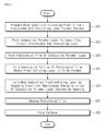
- FIG. 3 is a process flowchart according to the method of forming the pixel structure 100 of the active matrix display of FIG. 2 .
- FIGS. 4 to 9 are cross-sectional views illustrating each process according to the method of FIG. 3 .
- a base substrate 10 on which a plurality of pixel circuit electrodes 20 and an insulating layer 30 are formed may be prepared in S81.
- the pixel circuit electrodes 20 may be exposed through contact holes 32 of the insulating layer 30.
- a conductive polymer layer 40a may be formed to cover the pixel circuit electrodes 20 and the insulating layer 30 in S83.
- a conductive polymer for forming the conductive polymer layer 40a PEDT/PSS or PEDOT/PSS may be used.
- a solution process such as inkjet printing, spin coating, slit coating, or screen printing, may be used.
- a photoresist film 60 may be formed on the conductive polymer layer 40a in S85.
- an opening 61 may be formed in a portion of the photoresist film 60 where a pixel-defining layer 43 is to be formed. That is, the opening 61 may be formed by removing the portion of the photoresist film 60 where the pixel-defining layer 43 is to be formed through an exposure and developing process on the photoresist film 60.
- the non-conductive pixel-defining layer 43 may be formed by changing the characteristic of electrical resistance of a portion of the conductive polymer layer exposed by the opening 61.
- a wet-etch method or an ultraviolet light irradiation method may be used. That is, by immersing the base substrate 10 into a solution capable of changing electrical properties of the conductive polymer, the portion of the conductive polymer layer exposed by the opening 61 of the photoresist film 60 may be chemically changed to be non-conductive.
- the portion of the conductive polymer layer exposed by the opening 61 of the photoresist film 60 may be irradiated with ultraviolet light to be physically and chemically changed and the characteristic of electrical resistance thereof may become non-conductive.
- portions of the conductive polymer layer covered by the photoresist film 60 may maintain electrically conductive characteristics. Since the portion of the conductive polymer layer exposed by the opening 61 becomes the pixel-defining layer 43, the portion of the conductive polymer layer covered by the photoresist film 60 may be defined as pixel electrodes 41 by the pixel-defining layer 43.
- the pixel electrodes 41 and the pixel-defining layer 43 may be formed to be coplanar using the conductive polymer layer.
- the photoresist film is removed from the composite layer 40 including the plurality of pixel electrodes 41 and the pixel-defining layer 43.
- the pixel electrodes 41 and the pixel-defining layer 43 may be formed on the conductive polymer layer at the same time in one photolithography process using the photoresist layer. Since the pixel electrodes 41 and the pixel-defining layer 43 are integrally formed based on the conductive polymer, interfaces between the pixel electrodes 41 and the pixel-defining layer 43 may be formed to be continuous. Thus, formation of steps of edges of the pixel electrodes 41 may be fundamentally blocked.
- a cathode layer 70 is formed on the composite layer 40, and the pixel structure 100 of the active matrix display according to the embodiment of the present invention may be fabricated.
- the pixel structure 100 of the active matrix display may include the composite layer 40 in which the pixel electrodes 41 and the pixel-defining layer 43 are formed at the same time with no additional patterning process, since the conductive polymer layer 40a to form the pixel electrodes 41 and the pixel-defining layer 43 are formed on the insulating layer 30 including the pixel circuit electrodes 20, followed by changing the characteristic of electrical resistance of the portion to be the pixel-defining layer 43 in the conductive polymer layer 40a from conductive to non-conductive.
- a process of forming the pixel electrodes 41 and the pixel-defining layer 43 may be simplified.
- yield may be improved since exposure of steps of edges of the pixel electrodes due to a conventional patterning process is fundamentally prevented by changing the characteristic of electrical resistance of the portion to be the pixel-defining layer 43 in the conductive polymer layer 40a from conductive to non-conductive. That is, since the pixel electrodes 41 and the pixel-defining layer 43 formed based on the conductive polymer layer 40a are integrally formed, steps due to a conventional patterning process may not be generated located in the outskirts of pixel electrodes 43, and thus problems due to the exposure of steps may be fundamentally eliminated.
- PEDT/PSS or PEDOT/PSS instead of an organic material is used as the conductive composite layer 40
- a problem in which reliability of the active matrix display is degraded due to moisture generated by using the conventional organic material as the pixel-defining layer may be solved. That is, since PEDT/PSS or PEDOT/PSS instead of the organic material is used as the conductive composite layer 40, the problem due to moisture is suppressed and reliability of the active matrix display may be improved.
- the pixel electrodes 41 and the pixel-defining layer 43 are integrally formed in one layer using the conductive polymer layer 40a, the pixel electrodes 41 and the pixel-defining layer 43 may be formed at the same level and a short circuit problem occurring in interfaces between the pixel electrodes 41 and the pixel-defining layer 43 may be solved.
Landscapes
- Engineering & Computer Science (AREA)
- Manufacturing & Machinery (AREA)
- Microelectronics & Electronic Packaging (AREA)
- Physics & Mathematics (AREA)
- Chemical & Material Sciences (AREA)
- Materials Engineering (AREA)
- General Physics & Mathematics (AREA)
- Theoretical Computer Science (AREA)
- Computer Hardware Design (AREA)
- Optics & Photonics (AREA)
- Devices For Indicating Variable Information By Combining Individual Elements (AREA)
- Electroluminescent Light Sources (AREA)
Abstract
Description
- The present invention relates to an active matrix display. More specifically, the present invention relates to a pixel structure of an active matrix display in which a pixel electrode and a pixel defining layer are formed in a single layer, and a method of fabricating the same.
- Active matrix displays are display devices including a plurality of pixels arranged in the form of a matrix, and have been widely used in various applications. Such active matrix displays includes a panel having the pixels and a peripheral circuit to control the panel.
- Active matrix displays have advantages, such as a small thickness, a light weight, and low power consumption, and have been widely used as display devices for audio/video (AV) apparatuses, office automation apparatuses, and the like.
- Active matrix displays display information using light generated by pixel electrodes formed in an active matrix substrate. For example, an active matrix organic light-emitting diode (AMOLED) among the active matrix displays is a self-emissive display using a principle in which when current flows through a fluorescent or phosphor organic thin-film, electrons and holes are combined in the organic thin-film to generate light. Here, a color of light may vary depending on organic materials forming a light-emitting layer. An organic light-emitting diode (OLED) may be divided into a passive matrix light-emitting diode (PM OLED) and a passive matrix light-emitting diode (AMOLED). AMOLED is an individual-driving type in which each light-emitting device is driven, compared with PMOLED, a line-driving type in which a full line is driven to emit light.
- As illustrated in
FIG. 1 , apixel structure 200 of a normal active matrix display has a structure in which a plurality ofpixel electrodes 140 defined by a pixel-defininglayer 150 are arranged in the form of a matrix on abase substrate 110. - The
pixel structure 200 of the normal active matrix display may include thebase substrate 110, a plurality ofpixel circuit electrodes 120, abottom insulating layer 130, the plurality ofpixel electrodes 140, the pixel-defininglayer 150, and acathode layer 170. The plurality ofpixel circuit electrodes 120 may be formed in the form of a matrix on thebase substrate 110. Thebottom insulating layer 130 may be formed between the plurality ofpixel circuit electrodes 120, and thepixel circuit electrodes 120 may be exposed to the outside throughcontact holes 132 formed in thebottom insulating layer 130. The plurality of pixel electrodes 140a may be formed in the form of a matrix on the bottominsulating layer 130 and respectively connected to the plurality ofpixel circuit electrodes 120. The insulating pixel-defininglayer 150 may be formed between the plurality ofpixel electrodes 140. In addition, thecathode layer 170 may be formed to cover the plurality ofpixel electrodes 140 and the pixel-defininglayer 150. - Here, the
pixel electrodes 140 and the pixel-defininglayer 150 may be independently formed by patterning using photolithography processes. - That is, the
pixel electrodes 140 may be formed to be respectively connected to the plurality ofpixel circuit electrodes 120 by patterning using a photolithography process, after forming an electrode layer for forming thepixel electrodes 140 on thebottom insulating layer 130 including thepixel circuit electrodes 120. - Next, a top insulating layer for forming the pixel-defining
layer 150 may be formed to cover thebottom insulating layer 130 including thepixel electrodes 140. Then, the pixel-defininglayer 150 covering edges of the plurality ofpixel electrodes 140 may be formed by patterning using a photolithography process, - In such a manner, the
pixel structure 200 of the normal active matrix display normal may require separate patterning processes using separate photolithography processes to form thepixel electrodes 140 and the pixel-defininglayer 150. Thus, a manufacturing process may be complicated, and yield may be lowered due to the complicated process. - The
pixel electrodes 140 may includesteps 141 of edges thereof exposed by the patterning process. Although the pixel-defininglayer 150 such as an organic insulating layer is formed to cover thesteps 141 of thepixel electrodes 140 in order to solve a problem such as a short circuit with thecathode layer 170 formed on thepixel electrodes 140, thepixel electrodes 140 may still includesteps 141 of the edges thereof and still have the short circuit with thecathode layer 170 formed on thepixel electrodes 140. - In order to suppress such a short circuit problem between the
pixel electrodes 140 and thecathode layer 170, the pixel-defininglayer 150 needs to be formed in consideration of an inclination angle formed by the edges of thepixel electrodes 140 and the pixel-defininglayer 150, a height of each step, etc. Thus, the process of defining thepixel electrodes 140 may require considerably high skills. - In addition, since the pixel-defining
layer 150 is formed of an insulating material such as a hygroscopic organic material, reliability of the active matrix display may be lowered due to moisture included in the pixel-defininglayer 150. - Further, since the pixel-defining
layer 150 may be formed at a higher level than thepixel electrodes 140, efficiency of thepixel electrodes 140 may be reduced compared to a case in which thepixel electrodes 140 and the pixel-defininglayer 150 are formed at the same level. - Accordingly, the present invention is directed to a pixel structure of an active matrix display capable of simplifying a process of forming pixel electrodes and a pixel-defining layer, and a method fabricating the same.
- The present invention is also directed to a pixel structure of an active matrix display capable of improving yield by fundamentally preventing exposure of steps of edges of the pixel electrodes, and a method fabricating the same.
- The present invention is also directed to a pixel structure of an active matrix display capable of solving a problem in which reliability of the active matrix display is degraded due to moisture generated by using an organic material as a pixel-defining layer, and a method fabricating the same.
- The present invention is also directed to a pixel structure of an active matrix display capable of solving a problem such as a short circuit with a cathode layer occurring in interfaces between pixel electrodes and a pixel-defining layer, by forming the pixel-defining layer and the pixel-defining layer at the same level, and a method fabricating the same.
- According to an aspect of the present invention, there is provided a pixel structure of an active matrix display including a base substrate, a plurality of pixel circuit electrodes, an insulating layer, and a composite layer. The plurality of pixel circuit electrodes are arranged in the form of a matrix on the base substrate. The insulating layer is formed on the base substrate to cover outskirts of the plurality of pixel circuit electrodes. The composite layer is integrally formed to cover the plurality of pixel circuit electrodes and the insulating layer. Here, the composite layer includes conductive pixel electrodes respectively connected to the plurality of pixel circuit electrodes exposed in the insulating layer, and a non-conductive pixel-defining layer disposed around the pixel electrodes.
- In some embodiments, the composite layer may be formed based on conductive polyethylene dioxythiophene/polystyrene sulfonate (PEDT/PSS) or poly(3,4-ethylenedioxythiophene)/polystyrene sulfonate (PEDOT/PSS), the pixel-defining layer may be formed by changing the characteristic of electrical resistance of the conductive PEDT/PSS or PEDOT/PSS, and the pixel electrodes may be formed of the remaining conductive PEDT/PSS or PEDOT/PSS.
- In other embodiments, the pixel electrodes and the pixel-defining layer may be formed to be coplanar.
- According to another aspect of the present invention, there is provided a method of forming a pixel structure of an active matrix display including providing a base substrate including a plurality of pixel circuit electrodes and an insulating layer formed on an upper surface thereof, and forming an integrated composite layer to cover the plurality of pixel circuit electrodes and the insulating layer. The composite layer includes conductive pixel electrodes respectively connected to the plurality of pixel circuit electrodes exposed by the insulating layer, and a non-conductive pixel-defining layer disposed around the pixel electrodes.
- In some embodiments, the forming of the composite layer may include forming a conductive polymer layer configured to cover the plurality of pixel circuit electrodes and the insulating layer, forming a photoresist film on the conductive polymer layer, forming an opening by removing the photoresist film on a portion to be the pixel-defining layer in the conductive polymer layer, forming the non-conductive pixel-defining layer by changing the characteristic of electrical resistance of the portion of the conductive polymer layer exposed by the opening, removing the photoresist film, and forming a cathode layer on the composite layer.
- In other embodiments, when forming the non-conductive pixel-defining layer, portions covered by the photoresist film in the conductive polymer layer may be defined as the pixel electrodes by the pixel-defining layer.
- In other embodiments, the composite layer may be formed based on conductive polyethylene dioxythiophene/polystyrene sulfonate (PEDT/PSS) or poly(3,4-ethylenedioxythiophene)/polystyrene sulfonate (PEDOT/PSS), the pixel-defining layer may be formed by changing the characteristic of electrical resistance of the conductive PEDT/PSS or PEDOT/PSS, and the pixel electrodes may be formed of the remaining conductive PEDT/PSS or PEDOT/PSS.
- In other embodiments, the pixel electrodes and the pixel-defining layer may be formed to be coplanar.
- According to the embodiment of the present invention, a composite layer in which pixel electrodes and a pixel-defining layer are formed at the same time with no additional patterning process may be fabricated by forming a conductive polymer layer to form the pixel electrodes and the pixel-defining layer on an insulating layer including pixel circuit electrodes, and changing the characteristic of electrical resistance of a portion to be the pixel-defining layer in the conductive polymer layer from conductive to non-conductive. Thus, a process of forming the pixel electrodes and the pixel-defining layer may be simplified.
- In addition, yield may be improved since exposure of steps of edges of the pixel electrodes due to a conventional patterning process is fundamentally prevented by changing the characteristic of electrical resistance of the portion to be the pixel-defining layer in the conductive polymer layer from conductive to non-conductive. That is, since the pixel electrodes and the pixel-defining layer formed based on the conductive polymer layer are integrally formed, steps due to a conventional patterning process may not be generated located in the outskirts of pixel electrodes, and thus problems due to the exposure of steps may be fundamentally eliminated.
- In addition, according to the embodiment of the present invention, since polyethylene dioxythiophene/polystyrene sulfonate (PEDT/PSS) or poly(3,4-ethylenedioxythiophene)/polystyrene sulfonate (PEDOT/PSS) instead of an organic material is used as the conductive composite layer, a problem in which reliability of the active matrix display is degraded due to moisture generated by using the conventional organic material as the pixel-defining layer may be solved. That is, since PEDT/PSS or PEDOT/PSS instead of an organic material is used as the conductive composite layer, the problem due to moisture is suppressed and reliability of the active matrix display may be improved.
- Further, according to the embodiment of the present invention, since the pixel electrodes and the pixel-defining layer are integrally formed in one layer using the conductive polymer layer, the pixel electrodes and the pixel-defining layer may be disposed at the same level, and a short circuit problem occurring in interfaces between the pixel electrodes and the pixel-defining layer may be solved.
-
-
FIG. 1 is a cross-sectional view illustrating a pixel structure of an active matrix display according to a normal technology. -
FIG. 2 is a cross-sectional view illustrating a pixel structure of an active matrix display according to an embodiment of the present invention. -
FIG. 3 is a process flowchart according to a method of forming the pixel structure of the active matrix display ofFIG. 2 . -
FIGS. 4 to 9 are cross-sectional views illustrating each process according to the method ofFIG. 3 . - The objects, features, and advantages of the present invention will be more clearly understood from the following detailed descriptions of embodiments taken in conjunction with the accompanying drawings. In the following description, detailed descriptions of related known functions or elements that may unnecessarily make the gist of the present invention obscure will be omitted.
- The terms and words used in the specification and claims should not be construed with common or dictionary meanings, but construed as meanings and conception coinciding the spirit of the invention based on a principle that the inventors can appropriately define the concept of the terms to explain the invention in the optimum method. Therefore, embodiments described in the specification and the configurations shown in the drawings are not more than the most preferred embodiments of the present invention and do not fully cover the spirit of the present invention. Accordingly, it should be understood that there may be various equivalents and modifications that can replace those when this application is filed.
- Hereinafter, various embodiments will now be described more fully with reference to the accompanying drawings.
-
FIG. 2 is a cross-sectional view illustrating a pixel structure of an active matrix display according to an embodiment of the present invention. - Referring to
FIG. 2 , apixel structure 100 of an active matrix display according to an embodiment of the present invention includes abase substrate 10, a plurality ofpixel circuit electrodes 20, an insulatinglayer 30, and acomposite layer 40. Thecomposite layer 40 includes a plurality ofpixel electrodes 41 and a pixel-defininglayer 43. The plurality ofpixel circuit electrodes 20 may be arranged on thebase substrate 10 in the form of a matrix. The insulatinglayer 30 is formed on thebase substrate 10 to cover edges of the plurality ofpixel circuit electrodes 20. In addition, thecomposite layer 40 is integrally formed to cover the plurality ofpixel circuit electrodes 20 and the insulatinglayer 30. Here, thecomposite layer 40 includes theconductive pixel electrodes 41 respectively connected to the plurality ofpixel circuit electrodes 20 exposed by the insulatinglayer 30 and the non-conductive pixel-defininglayer 43 disposed around thepixel electrodes 41. Thepixel structure 100 of the active matrix display according to the embodiment of the present invention may further include acathode layer 70 formed on thecomposite layer 40. - As the
base substrate 10, a glass substrate, a plastic substrate, or a metal substrate may be used. Here, the glass substrate may be formed of silicon oxide, silicon nitride, etc. The plastic substrate may be formed of an insulating organic material. For example, the plastic substrate may be formed of an organic material selected from the group consisting of polyethersulfone (PES), polyacrylate (PAR), polyetherimide (PEI), polyethylene naphthalate (PEN), polyethylene terephthalate (PET), polyphenylene sulfide (PPS), polyarylate, polyimide, polycarbonate (PC), cellulose triacetate (CTA), and cellulose acetate propionate (CAP), but is not limited thereto. The metal substrate may include at least one selected from the group consisting of carbon(C), iron (Fe), chrome (Cr), manganese (Mn), nickel (Ni), titanium (Ti), molybdenum (Mo), stainless steel (SUS), an Invar alloy, a ZInconel alloy, and a Kovar alloy, but is not limited thereto. The metal substrate may be a metal foil. In order for thebase substrate 10 to have flexible characteristics, the plastic substrate or the metal substrate may be used. - The plurality of
pixel circuit electrodes 20 may be a thin film transistor (TFT) used in an active matrix display. Although not shown inFIG. 2 , thepixel circuit electrodes 20 may mainly consist of an amorphous silicon semiconductor material or a polysilicon semiconductor material, a silicon oxide insulating layer, and a metal electrode. As thepixel circuit electrodes 20, an organic thin film transistor (OTFT) using an organic material may be used. - The insulating
layer 30 may be formed on thebase substrate 10 and the plurality ofpixel circuit electrodes 20, and contact holes 32 may be formed to expose thepixel circuit electrodes 20. Through the contact holes 32, thepixel electrodes 41 may be electrically connected to thepixel circuit electrodes 20. An inorganic insulating material or an organic insulating material may be used as the insulatinglayer 30. Here, the inorganic insulating material used as the insulatinglayer 30 may be SiO2. More specifically, spin-on-glass (SOG) including one selected from the group consisting of siloxane, silazane, and silicate, or spin-on-dielectric (SOD) including polysilazane, which are capable of forming silicon oxide through a solution process, may be used. The organic insulating material used as the insulatinglayer 30 may be parylene, epoxy, polyimide (PI), polyamide (PA), polyvinyl chloride (PVC), benzocyclobutene (BCB), polyvinyl alcohol (PVA), polyvinylphenol (PVP), or cyclopentane (CyPe). As a method of forming the insulatinglayer 30, a solution process, such as inkjet printing, spin coating, slit coating, or screen printing, may be used. The contact holes 32 may be formed by photolithography and an etching process. - In addition, the
composite layer 40 is formed based on a conductive polymer, and the plurality ofpixel electrodes 41 and the pixel-defininglayer 43 are integrally formed to be coplanar. Such acomposite layer 40 may be formed based on a conductive polymer layer formed of a conductive polymer, such as conductive polyethylene dioxythiophene/polystyrene sulfonate (PEDT/PSS) or poly(3,4-ethylenedioxythiophene)/polystyrene sulfonate (PEDOT/PSS). In the conductive polymer layer, the pixel-defininglayer 43 may be formed by changing the characteristic of electrical resistance of the conductive polymer from conductive to non-conductive, and the plurality ofpixel electrodes 41 may be formed of the remaining conductive polymer. - Here, as a method of changing the characteristic of electrical resistance of the conductive polymer from conductive to non-conductive, only a portion to form the pixel-defining
layer 43 in the conductive polymer may be locally wet etched or locally irradiated with ultraviolet light. - Thus, in the
pixel structure 100 of the active matrix display according to the embodiment of the present invention, since the pixel-defininglayer 43 and thepixel electrodes 41 may be formed together using the conductive polymer layer configured to form thepixel electrodes 41, a conventional process of forming the pixel-defininglayer 43 using an organic insulating material may be omitted. - In addition, in the
pixel structure 100 of the active matrix display according to the embodiment of the present invention, since thepixel electrodes 41 and the pixel-defininglayer 43 are formed to be coplanar, efficiency of thepixel electrodes 41 may be improved. - A method of forming the
pixel structure 100 of the active matrix display according to the embodiment of the present invention will be described as follows with reference toFIGS. 2 to 8 . Here,FIG. 3 is a process flowchart according to the method of forming thepixel structure 100 of the active matrix display ofFIG. 2 . In addition,FIGS. 4 to 9 are cross-sectional views illustrating each process according to the method ofFIG. 3 . - First, as illustrated in
FIG. 4 , abase substrate 10 on which a plurality ofpixel circuit electrodes 20 and an insulatinglayer 30 are formed may be prepared in S81. Thepixel circuit electrodes 20 may be exposed through contact holes 32 of the insulatinglayer 30. - Next, as illustrated in
FIG. 5 , aconductive polymer layer 40a may be formed to cover thepixel circuit electrodes 20 and the insulatinglayer 30 in S83. Here, as a conductive polymer for forming theconductive polymer layer 40a, PEDT/PSS or PEDOT/PSS may be used. As a method of forming theconductive polymer layer 40a, a solution process, such as inkjet printing, spin coating, slit coating, or screen printing, may be used. - Next, as illustrated in
FIG. 6 , aphotoresist film 60 may be formed on theconductive polymer layer 40a in S85. - Next, as illustrated in
FIG. 7 , in S87, anopening 61 may be formed in a portion of thephotoresist film 60 where a pixel-defininglayer 43 is to be formed. That is, theopening 61 may be formed by removing the portion of thephotoresist film 60 where the pixel-defininglayer 43 is to be formed through an exposure and developing process on thephotoresist film 60. - Next, as illustrated in
FIG. 8 , in S89, the non-conductive pixel-defininglayer 43 may be formed by changing the characteristic of electrical resistance of a portion of the conductive polymer layer exposed by theopening 61. Here, in order to change the characteristic of electrical resistance of the portion of the conductive polymer exposed by the opening 61 from conductive to non-conductive, a wet-etch method or an ultraviolet light irradiation method may be used. That is, by immersing thebase substrate 10 into a solution capable of changing electrical properties of the conductive polymer, the portion of the conductive polymer layer exposed by theopening 61 of thephotoresist film 60 may be chemically changed to be non-conductive. Alternatively, the portion of the conductive polymer layer exposed by theopening 61 of thephotoresist film 60 may be irradiated with ultraviolet light to be physically and chemically changed and the characteristic of electrical resistance thereof may become non-conductive. - Here, portions of the conductive polymer layer covered by the
photoresist film 60 may maintain electrically conductive characteristics. Since the portion of the conductive polymer layer exposed by theopening 61 becomes the pixel-defininglayer 43, the portion of the conductive polymer layer covered by thephotoresist film 60 may be defined aspixel electrodes 41 by the pixel-defininglayer 43. - Thus, according to the embodiment of the present invention, the
pixel electrodes 41 and the pixel-defininglayer 43 may be formed to be coplanar using the conductive polymer layer. - Next, as illustrated in
FIG. 9 , in S91, the photoresist film is removed from thecomposite layer 40 including the plurality ofpixel electrodes 41 and the pixel-defininglayer 43. - In this manner, the
pixel electrodes 41 and the pixel-defininglayer 43 may be formed on the conductive polymer layer at the same time in one photolithography process using the photoresist layer. Since thepixel electrodes 41 and the pixel-defininglayer 43 are integrally formed based on the conductive polymer, interfaces between thepixel electrodes 41 and the pixel-defininglayer 43 may be formed to be continuous. Thus, formation of steps of edges of thepixel electrodes 41 may be fundamentally blocked. - In addition, as illustrated in
FIG. 2 , in S93, acathode layer 70 is formed on thecomposite layer 40, and thepixel structure 100 of the active matrix display according to the embodiment of the present invention may be fabricated. - The
pixel structure 100 of the active matrix display according to the embodiment of the present invention may include thecomposite layer 40 in which thepixel electrodes 41 and the pixel-defininglayer 43 are formed at the same time with no additional patterning process, since theconductive polymer layer 40a to form thepixel electrodes 41 and the pixel-defininglayer 43 are formed on the insulatinglayer 30 including thepixel circuit electrodes 20, followed by changing the characteristic of electrical resistance of the portion to be the pixel-defininglayer 43 in theconductive polymer layer 40a from conductive to non-conductive. Thus, a process of forming thepixel electrodes 41 and the pixel-defininglayer 43 may be simplified. - In addition, yield may be improved since exposure of steps of edges of the pixel electrodes due to a conventional patterning process is fundamentally prevented by changing the characteristic of electrical resistance of the portion to be the pixel-defining
layer 43 in theconductive polymer layer 40a from conductive to non-conductive. That is, since thepixel electrodes 41 and the pixel-defininglayer 43 formed based on theconductive polymer layer 40a are integrally formed, steps due to a conventional patterning process may not be generated located in the outskirts ofpixel electrodes 43, and thus problems due to the exposure of steps may be fundamentally eliminated. - In addition, according to the embodiment of the present invention, since PEDT/PSS or PEDOT/PSS instead of an organic material is used as the conductive
composite layer 40, a problem in which reliability of the active matrix display is degraded due to moisture generated by using the conventional organic material as the pixel-defining layer may be solved. That is, since PEDT/PSS or PEDOT/PSS instead of the organic material is used as the conductivecomposite layer 40, the problem due to moisture is suppressed and reliability of the active matrix display may be improved. - Further, according to the embodiment of the present invention, since the
pixel electrodes 41 and the pixel-defininglayer 43 are integrally formed in one layer using theconductive polymer layer 40a, thepixel electrodes 41 and the pixel-defininglayer 43 may be formed at the same level and a short circuit problem occurring in interfaces between thepixel electrodes 41 and the pixel-defininglayer 43 may be solved. - Although a few embodiments have been described, it will be apparent to those skilled in the art that various modifications can be made to the above-described exemplary embodiments of the present invention without departing from the spirit or scope of the invention.
Claims (8)
- A pixel structure of an active matrix display, comprising:a base substrate;a plurality of pixel circuit electrodes arranged in the form of a matrix on the base substrate;an insulating layer formed on the base substrate to cover edges of the plurality of pixel circuit electrodes; anda composite layer integrally formed to cover the plurality of pixel circuit electrodes and the insulating layer, wherein the composite layer includes conductive pixel electrodes respectively connected to the plurality of pixel circuit electrodes exposed in the insulating layer, and a non-conductive pixel-defining layer disposed around the pixel electrodes.
- The pixel structure of an active matrix display of claim 1, wherein the composite layer is formed based on conductive polyethylene dioxythiophene/polystyrene sulfonate (PEDT/PSS) or poly(3,4-ethylenedioxythiophene)/polystyrene sulfonate (PEDOT/PSS), the pixel-defining layer is formed by changing the characteristic of electrical resistance of the conductive PEDT/PSS or PEDOT/PSS, and the pixel electrodes are formed of the remaining conductive PEDT/PSS or PEDOT/PSS.
- The pixel structure of an active matrix display of claim 2, wherein the pixel electrodes and the pixel-defining layer are formed to be coplanar.
- A method of forming a pixel structure of an active matrix display, comprising:providing a base substrate including a plurality of pixel circuit electrodes and an insulating layer formed on an upper surface thereof; andforming an integrated composite layer to cover the plurality of pixel circuit electrodes and the insulating layer, wherein the composite layer includes conductive pixel electrodes respectively connected to the plurality of pixel circuit electrodes exposed by the insulating layer, and a non-conductive pixel-defining layer disposed around the pixel electrodes.
- The method of claim 4, wherein the forming of the composite layer comprises;
forming a conductive polymer layer configured to cover the plurality of pixel circuit electrodes and the insulating layer;
forming a photoresist film on the conductive polymer layer;
forming an opening by removing the photoresist film on a portion to be the pixel-defining layer in the conductive polymer layer;
forming the non-conductive pixel-defining layer by changing the characteristic of electrical resistance of the portion of the conductive polymer layer exposed by the opening; and
removing the photoresist film. - The method of claim 5, wherein when forming the non-conductive pixel-defining layer, portions covered by the photoresist film in the conductive polymer layer are defined as the pixel electrodes by the pixel-defining layer.
- The method of claim 5, wherein the composite layer is formed based on conductive polyethylene dioxythiophene/polystyrene sulfonate (PEDT/PSS) or poly(3,4-ethylenedioxythiophene)/polystyrene sulfonate (PEDOT/PSS), the pixel-defining layer is formed by changing the characteristic of electrical resistance of the conductive PEDT/PSS or PEDOT/PSS, and the pixel electrodes are formed of the remaining conductive PEDT/PSS or PEDOT/PSS.
- The method of claim 4, wherein the pixel electrodes and the pixel-defining layer are formed to be coplanar.
Applications Claiming Priority (2)
| Application Number | Priority Date | Filing Date | Title |
|---|---|---|---|
| KR1020120141829A KR101402606B1 (en) | 2012-12-07 | 2012-12-07 | Structure of pixel for active matrix display and the method |
| PCT/KR2013/011067 WO2014088275A1 (en) | 2012-12-07 | 2013-12-02 | Pixel structure for active matrix display, and method for manufacturing same |
Publications (2)
| Publication Number | Publication Date |
|---|---|
| EP2930761A1 true EP2930761A1 (en) | 2015-10-14 |
| EP2930761A4 EP2930761A4 (en) | 2016-07-20 |
Family
ID=50883650
Family Applications (1)
| Application Number | Title | Priority Date | Filing Date |
|---|---|---|---|
| EP13860909.4A Withdrawn EP2930761A4 (en) | 2012-12-07 | 2013-12-02 | PIXEL STRUCTURE FOR ACTIVE MATRIX DISPLAY AND METHOD OF MANUFACTURING THE SAME |
Country Status (7)
| Country | Link |
|---|---|
| US (1) | US20150311267A1 (en) |
| EP (1) | EP2930761A4 (en) |
| JP (1) | JP2016508230A (en) |
| KR (1) | KR101402606B1 (en) |
| CN (1) | CN104981917A (en) |
| TW (1) | TW201428944A (en) |
| WO (1) | WO2014088275A1 (en) |
Families Citing this family (7)
| Publication number | Priority date | Publication date | Assignee | Title |
|---|---|---|---|---|
| GB2513165A (en) * | 2013-04-18 | 2014-10-22 | British American Tobacco Co | Container |
| CN103700685B (en) * | 2013-12-12 | 2017-12-08 | 京东方科技集团股份有限公司 | A kind of display panel, display device |
| JP2015201354A (en) * | 2014-04-08 | 2015-11-12 | 株式会社ジャパンディスプレイ | Organic EL display device |
| KR102587708B1 (en) * | 2016-06-30 | 2023-10-11 | 엘지디스플레이 주식회사 | Organic light emitting display device, head mounted display including the same and method for manufacturing the same |
| CN107123751B (en) * | 2017-04-28 | 2019-04-16 | 武汉华星光电技术有限公司 | A kind of flexible organic light emitting diode display and preparation method thereof |
| CN110164944A (en) * | 2019-06-03 | 2019-08-23 | 京东方科技集团股份有限公司 | Display base plate and its manufacturing method, mask plate, display device |
| CN111403623A (en) * | 2020-03-26 | 2020-07-10 | 武汉华星光电半导体显示技术有限公司 | Display panel and preparation method thereof |
Family Cites Families (11)
| Publication number | Priority date | Publication date | Assignee | Title |
|---|---|---|---|---|
| KR100769161B1 (en) * | 2001-03-05 | 2007-10-23 | 엘지.필립스 엘시디 주식회사 | LCD and its manufacturing method |
| JP5147215B2 (en) | 2006-10-31 | 2013-02-20 | 株式会社日立製作所 | Pixel drive circuit for display element and display device using the same |
| US20100295036A1 (en) * | 2008-02-01 | 2010-11-25 | E.I. Du Pont De Nemours And Company | Structure for making solution processed electronic devices |
| KR100918403B1 (en) * | 2008-02-12 | 2009-09-24 | 삼성모바일디스플레이주식회사 | OLED display device and manufacturing method thereof |
| TWI358820B (en) * | 2008-02-29 | 2012-02-21 | Chunghwa Picture Tubes Ltd | Active device array substrate and fabrication meth |
| KR101058112B1 (en) * | 2009-10-20 | 2011-08-24 | 삼성모바일디스플레이주식회사 | Organic light emitting display device |
| JP5500978B2 (en) | 2009-12-25 | 2014-05-21 | 株式会社ジャパンディスプレイ | Organic EL device |
| KR101084191B1 (en) * | 2010-02-16 | 2011-11-17 | 삼성모바일디스플레이주식회사 | Organic light emitting display device and manufacturing method thereof |
| KR101146991B1 (en) * | 2010-05-07 | 2012-05-23 | 삼성모바일디스플레이주식회사 | Organic light emitting diode display apparatus and method of manufacturing the same |
| KR20120043438A (en) * | 2010-10-26 | 2012-05-04 | 삼성모바일디스플레이주식회사 | Organic light emitting display apparatus |
| US9178174B2 (en) * | 2012-03-27 | 2015-11-03 | Sony Corporation | Display device and method of manufacturing the same, method of repairing display device, and electronic apparatus |
-
2012
- 2012-12-07 KR KR1020120141829A patent/KR101402606B1/en not_active Expired - Fee Related
-
2013
- 2013-12-02 US US14/650,141 patent/US20150311267A1/en not_active Abandoned
- 2013-12-02 WO PCT/KR2013/011067 patent/WO2014088275A1/en not_active Ceased
- 2013-12-02 EP EP13860909.4A patent/EP2930761A4/en not_active Withdrawn
- 2013-12-02 CN CN201380063528.7A patent/CN104981917A/en active Pending
- 2013-12-02 JP JP2015546378A patent/JP2016508230A/en active Pending
- 2013-12-06 TW TW102144881A patent/TW201428944A/en unknown
Also Published As
| Publication number | Publication date |
|---|---|
| KR101402606B1 (en) | 2014-06-03 |
| CN104981917A (en) | 2015-10-14 |
| WO2014088275A1 (en) | 2014-06-12 |
| JP2016508230A (en) | 2016-03-17 |
| EP2930761A4 (en) | 2016-07-20 |
| TW201428944A (en) | 2014-07-16 |
| US20150311267A1 (en) | 2015-10-29 |
Similar Documents
| Publication | Publication Date | Title |
|---|---|---|
| US20150311267A1 (en) | Pixel structure for active matrix display, and method for manufacturing same | |
| KR102124025B1 (en) | Organic Light Emitting Diode Display Device and Method of Fabricating the Same | |
| US10411080B2 (en) | Flexible organic electroluminescent device and method for fabricating the same | |
| EP3139410B1 (en) | Amoled array substrate, manufacturing method thereof, and display device | |
| EP3664142B1 (en) | Pixel circuit, manufacturing method thereof, and display device | |
| JP6110063B2 (en) | Organic light emitting display device and method for manufacturing organic light emitting display device | |
| CN113241367B (en) | Display substrate and preparation method thereof | |
| CN102593144B (en) | Manufacture the method for bottom-beam organic light-emitting display device | |
| CN105448957A (en) | Organic electroluminescence display substrate and manufacturing method thereof and display device | |
| US20120097952A1 (en) | Organic Light-Emitting Display Apparatus | |
| KR20120092386A (en) | Organic light emitting display device and method for manufacturing the same | |
| KR20220088634A (en) | Display substrate, manufacturing method thereof, and display device | |
| CN101587939A (en) | Organic thin film transistor, pixel structure, manufacturing method of organic thin film transistor and pixel structure, and display panel | |
| WO2021093681A1 (en) | Display backplane, manufacturing method therefor, and display device | |
| JP2007134482A (en) | THIN FILM TRANSISTOR DEVICE, ITS MANUFACTURING METHOD, AND THIN FILM TRANSISTOR ARRAY AND THIN FILM TRANSISTOR DISPLAY USING THE SAME | |
| US20160079326A1 (en) | Pixel structure of electroluminescent display panel and method of fabricating the same | |
| KR20150075188A (en) | Organic Light Emitting Display and Method for Manufacturing The Same | |
| KR102114999B1 (en) | Organic Light Emitting Diode Display Device and Method for Manufacturing The Same | |
| US20070222375A1 (en) | System for displaying images including electroluminescent device and method for fabricating the same | |
| TW201411829A (en) | Organic electroluminescent display and method of manufacturing the same | |
| US20080032431A1 (en) | Method for fabricating a system for displaying images | |
| WO2014136150A1 (en) | El display device | |
| JP2009104859A (en) | Organic EL device and manufacturing method thereof | |
| JP4589830B2 (en) | Flexible display and manufacturing method thereof | |
| CN113571666A (en) | Display panel, method for producing the same, and display device |
Legal Events
| Date | Code | Title | Description |
|---|---|---|---|
| PUAI | Public reference made under article 153(3) epc to a published international application that has entered the european phase |
Free format text: ORIGINAL CODE: 0009012 |
|
| 17P | Request for examination filed |
Effective date: 20150529 |
|
| AK | Designated contracting states |
Kind code of ref document: A1 Designated state(s): AL AT BE BG CH CY CZ DE DK EE ES FI FR GB GR HR HU IE IS IT LI LT LU LV MC MK MT NL NO PL PT RO RS SE SI SK SM TR |
|
| AX | Request for extension of the european patent |
Extension state: BA ME |
|
| DAX | Request for extension of the european patent (deleted) | ||
| RA4 | Supplementary search report drawn up and despatched (corrected) |
Effective date: 20160617 |
|
| RIC1 | Information provided on ipc code assigned before grant |
Ipc: H01L 27/32 20060101ALI20160613BHEP Ipc: H01L 51/00 20060101ALI20160613BHEP Ipc: H01L 51/56 20060101ALI20160613BHEP Ipc: G09F 9/00 20060101ALI20160613BHEP Ipc: H01L 51/52 20060101ALI20160613BHEP Ipc: H01L 51/50 20060101AFI20160613BHEP |
|
| STAA | Information on the status of an ep patent application or granted ep patent |
Free format text: STATUS: REQUEST FOR EXAMINATION WAS MADE |
|
| STAA | Information on the status of an ep patent application or granted ep patent |
Free format text: STATUS: THE APPLICATION IS DEEMED TO BE WITHDRAWN |
|
| 18D | Application deemed to be withdrawn |
Effective date: 20170117 |