EP2929577B1 - Electrical device, in particular organic light emitting device. - Google Patents
Electrical device, in particular organic light emitting device. Download PDFInfo
- Publication number
- EP2929577B1 EP2929577B1 EP13802450.0A EP13802450A EP2929577B1 EP 2929577 B1 EP2929577 B1 EP 2929577B1 EP 13802450 A EP13802450 A EP 13802450A EP 2929577 B1 EP2929577 B1 EP 2929577B1
- Authority
- EP
- European Patent Office
- Prior art keywords
- detection layer
- protection element
- layer
- contact
- electrical device
- Prior art date
- Legal status (The legal status is an assumption and is not a legal conclusion. Google has not performed a legal analysis and makes no representation as to the accuracy of the status listed.)
- Active
Links
Images


Classifications
-
- G—PHYSICS
- G01—MEASURING; TESTING
- G01N—INVESTIGATING OR ANALYSING MATERIALS BY DETERMINING THEIR CHEMICAL OR PHYSICAL PROPERTIES
- G01N21/00—Investigating or analysing materials by the use of optical means, i.e. using sub-millimetre waves, infrared, visible or ultraviolet light
- G01N21/62—Systems in which the material investigated is excited whereby it emits light or causes a change in wavelength of the incident light
- G01N21/63—Systems in which the material investigated is excited whereby it emits light or causes a change in wavelength of the incident light optically excited
- G01N21/64—Fluorescence; Phosphorescence
- G01N21/6428—Measuring fluorescence of fluorescent products of reactions or of fluorochrome labelled reactive substances, e.g. measuring quenching effects, using measuring "optrodes"
- G01N21/643—Measuring fluorescence of fluorescent products of reactions or of fluorochrome labelled reactive substances, e.g. measuring quenching effects, using measuring "optrodes" non-biological material
-
- H—ELECTRICITY
- H10—SEMICONDUCTOR DEVICES; ELECTRIC SOLID-STATE DEVICES NOT OTHERWISE PROVIDED FOR
- H10K—ORGANIC ELECTRIC SOLID-STATE DEVICES
- H10K50/00—Organic light-emitting devices
- H10K50/80—Constructional details
- H10K50/84—Passivation; Containers; Encapsulations
-
- H—ELECTRICITY
- H10—SEMICONDUCTOR DEVICES; ELECTRIC SOLID-STATE DEVICES NOT OTHERWISE PROVIDED FOR
- H10K—ORGANIC ELECTRIC SOLID-STATE DEVICES
- H10K50/00—Organic light-emitting devices
- H10K50/80—Constructional details
- H10K50/84—Passivation; Containers; Encapsulations
- H10K50/844—Encapsulations
-
- G—PHYSICS
- G01—MEASURING; TESTING
- G01N—INVESTIGATING OR ANALYSING MATERIALS BY DETERMINING THEIR CHEMICAL OR PHYSICAL PROPERTIES
- G01N21/00—Investigating or analysing materials by the use of optical means, i.e. using sub-millimetre waves, infrared, visible or ultraviolet light
- G01N21/62—Systems in which the material investigated is excited whereby it emits light or causes a change in wavelength of the incident light
- G01N21/63—Systems in which the material investigated is excited whereby it emits light or causes a change in wavelength of the incident light optically excited
- G01N21/64—Fluorescence; Phosphorescence
- G01N21/6428—Measuring fluorescence of fluorescent products of reactions or of fluorochrome labelled reactive substances, e.g. measuring quenching effects, using measuring "optrodes"
- G01N2021/6439—Measuring fluorescence of fluorescent products of reactions or of fluorochrome labelled reactive substances, e.g. measuring quenching effects, using measuring "optrodes" with indicators, stains, dyes, tags, labels, marks
Definitions
- the invention relates to an electrical device comprising a protection element like a thin-film encapsulation (TFE) for protecting an electrical unit of the electrical device against water and/or oxygen.
- a protection element like a thin-film encapsulation (TFE) for protecting an electrical unit of the electrical device against water and/or oxygen.
- TFE thin-film encapsulation
- organic light emitting devices are very sensitive to moisture. For this reason organic light emitting devices generally comprise a TFE, which may comprise a single inorganic layer or a combination of inorganic and/or organic layers forming a multilayer stack.
- the TFE generally provides a good protection against moisture. However, the quality of the TFE barrier may be reduced due to pinholes or voids, thereby providing penetration pathways for moisture through the TFE.
- US 7,767,498 B2 discloses a system for testing the effectiveness of barrier structures.
- the system uses metallic calcium coupons on glass encapsulated with multilayer barrier stacks.
- the formation of transparent calcium oxide and hydroxide by permeation increases the transmission of visible light through the calcium coupon, which can be optically detected for determining a degree of permeability of the multilayer barrier stacks.
- This calcium test is technically relatively complex and takes a relatively long time.
- US 2006/0121613 A1 discloses an indicator layer between an oxygen sensitive product and a barrier layer.
- the indicator layer comprises e.g. porphyrin. Upon illumination of the film to activate the porphyrin, the porphyrin phosphoresces to a degree which is inversely proportional to the oxygen content on that location.
- US2011/0127498 A1 discloses an OLED device having a capping layer e.g. A1Q3 or NPB on top of the OLED and covered by a protective element.
- an electrical device comprising:
- the detection layer comprises organic material and changes its property, if it is in contact with the contact gas usable for detecting the permeability of the protection element and since this detection layer is arranged between the protection element and the electrical unit or within the protection element, a detection test for detecting a permeability of the protection element can easily be integrated into a production process for producing the electrical device, i.e. a time consuming external permeability test as disclosed in the above mentioned patent document US 7,767,498 B2 is not required.
- penetration paths for water, in particular for moisture, and/or oxygen through the protection element can be detected relatively fast during the production process by detecting the change of the property of the detection layer comprising the organic material. Particularly pinholes or other defects leading to penetration paths can be detected relatively fast.
- the monomer is preferentially an organic monomer like an organic photoresist.
- the polymerization is preferentially initiated by UV light. Using these detection layers allows detecting a contact with the contact gas with high accuracy, in particular spatially resolved.
- the contact gas is preferentially a gas selected from the group consisting of water, oxygen, ozone, fluorine, bromine, chlorine and combinations thereof. However, also other gases can be used, which can penetrate through defected parts of the protection element.
- the contact gas can be a gas having gas molecules being smaller or equal to the size of ozone molecules, further preferred smaller than or equal to the size of oxygen molecules, and even further preferred smaller than or equal to the size of water molecules.
- the electrical unit is preferentially an organic light emitting unit like an organic light emitting diode (OLED), and the protection element is preferentially a TFE, which may comprise a single inorganic layer or several inorganic and/or organic layers forming a multilayer stack.
- OLED organic light emitting diode
- TFE TFE
- the detection layer is adapted such that the property of the detection layer is locally changed at a location, at which the detection layer is in contact with the contact gas. This allows determining at which location a defect like a penetration path through the protection element is present, wherein then at the determined location the defect can be repaired.
- the detection layer is adapted to change its property by a chemical reaction with the contact gas.
- the chemical reaction is preferentially a photochemical reaction.
- For performing the photochemical reaction light having a certain wavelength may be used like ultraviolet (UV) light. This allows modifying the property of the detection layer in a relatively simple and reliable way such that a contact of the detection layer with the contact gas can be detected with relatively high accuracy.
- UV ultraviolet
- the detection layer is adapted to change its property such that the change is observable by an optical measuring device.
- the detection layer is adapted to change at least one of the group of photoluminescence, reflectivity and absorption, if the detection layer is in contact with with the contact gas, in particular with moisture and/or oxygen.
- the protection element may be at least partly transparent with respect to light used for optically detecting the property change. If the protection element is a TFE having multiple layers and if the detection layer is arranged in between these layers of the TFE, only one or several layers of the TFE arranged between the detection layer and a light source of the measuring device may be at least partly transparent to the light emitted by the light source, in order to allow the light to traverse these one or several layers of the TFE such that it can reach the detection layer for detecting a possible property change.
- the detection layer may have a thickness in the nanometer or micrometer range.
- the detection layer may comprise a photoluminescent organic layer which is adapted such that it degrades, if the detection layer is in contact with the contact gas, in order to change its property.
- the photoluminescent organic layer may be photodegradable, wherein it degrades, if the photoluminescent organic layer is illuminated by light and if it is in contact with the contact gas.
- the photoluminescent organic layer may be adapted to degrade, if the photoluminescent organic layer is illuminated by UV light and if it is in contact with the contact gas.
- the photoluminescent organic layer is, for instance, Tris-(8-hydroxyquinoline)aluminum (Alq 3 ).
- a detection apparatus for detecting a permeability of a protection element of an electrical device as defined in claim 1, wherein the protection element at least partly covers an electrical unit of the electrical device and is adapted to protect the electrical unit against water and/or oxygen comprises a measuring device for measuring a change in a property of a detection layer of the electrical device, which is generated, if the detection layer is in contact with a contact gas usable for detecting the permeability of the protection element.
- the measuring device is preferentially adapted to optically detect the change in the property of the layer.
- the measuring device is adapted to use one of the group of optical microscopy, optical spectroscopy, reflective measurements, absorption measurements and luminance measurements or combinations thereof, wherein the optical microscopy may be near field scanning optical microscopy (SNOM).
- a production apparatus for producing an electrical device as defined in claim 1 comprises:
- a detection method for detecting a permeability of a protection element of an electrical device as defined in claim 1, wherein the protection element at least partly covers an electrical unit of the electrical device and is adapted to protect the electrical unit against water and/or oxygen comprises the step of measuring a change in a property of a detection layer of the electrical device, which is generated, if the detection layer is in contact with a contact gas usable for detecting the permeability of the protection element.
- a production method for producing an electrical device as defined in claim 1 comprises the steps of:
- the detection layer and/or the protection layer may be provided by a deposition technique like thermal evaporation, sputtering, spin coating, chemical vapor deposition, atomic layer deposition or molecular layer deposition.
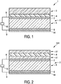
- Fig. 1 shows schematically and exemplarily an embodiment of an electrical device.
- the electrical device comprises an electrical unit 2 being, in this embodiment, an OLED.
- the OLED comprises a transparent anode 6 on a glass substrate 14, a cathode 7 and intermediate organic light emitting layers 5.
- the anode 6 and the cathode 7 are electrically connected to a voltage source 10 via electrical connections 8, 9.
- the electrical unit 2 can be another kind of OLED.
- the electrical unit 2 can also not be an OLED, but another electrical unit that should be protected against moisture and/or oxygen.
- the electrical device 1 further comprises a protection element 3, which covers the electrical unit 2, for protecting the electrical unit 2 against moisture and oxygen.
- the protection element is a TFE.
- the electrical device 1 comprises a detection layer 4 arranged between the TFE 3 and the electrical unit 2, wherein the detection layer 4 is adapted such that a property of the detection layer 4 is changed, if the detection layer 4 is in contact with moisture and/or oxygen.
- the detection layer 4 can also be arranged within the TFE as schematically and exemplarily shown in Fig. 2 .
- Fig. 2 a further embodiment of an electrical device 101 is shown, which is similar to the electrical device 1 shown in Fig. 1 , except for the TFE 11, 17 and the location of the detection layer 4.
- the TFE is a multilayer stack having at least two parts 11, 17, wherein the detection layer 4 is arranged between these two parts 11, 17 of the TFE.
- the TFE comprises one or several nitride and/or oxide layers.
- the TFE can comprise a layer selected from the group consisting of SiN x , AlO x , TiO x , ZrO x , HfO x , SiO x , SiON and combinations thereof.
- the TFE can also comprise layers made of other materials.
- the layers of the TFE have preferentially thicknesses in the range of 10 nm to several micrometers. If the TFE layers are deposited by using an atomic layer deposition technique, a layer of the several layers of the TFE can have a thickness being smaller than 10 nm.
- the detection layer comprises a monomer, which polymerizes if illuminated and if in contact with moisture and/or oxygen, in order to change the property of the detection layer.
- the monomer is preferentially an organic monomer like an organic photoresist, wherein the polymerization is preferentially initiated by UV light.
- the detection layer 4 is adapted such that the property of the detection layer 4 is locally changed at a location, at which the detection layer 4 is in contact with moisture and/or oxygen.
- This property change can be provided by a chemical, in particular a photochemical reaction, with moisture, i.e. water, and/or oxygen.
- For performing the photochemical reaction light having a certain wavelength like UV light may be used.
- the property change is then preferentially observable by an optical measuring device.
- the photoluminescence and/or the reflectivity and/or the absorption of the detection layer can be modified at the location, at which the detection layer is in contact with moisture and/or oxygen, wherein this change in photoluminescence and/or reflectivity and/or absorption can be detected by the optical measuring device.
- the detection layer 4 has a thickness in the nanometer or micrometer range and comprises an organic material and optionally additionally inorganic material.
- the detection layer may comprise a photoluminescent organic layer which is adapted such that it degrades, if the detection layer 4 is in contact with moisture and/or oxygen.
- the photoluminescent organic layer is preferentially photodegradable, wherein it degrades, if the photoluminescent organic layer is illuminated by light and if it is in contact with moisture and/or oxygen.
- this light can be UV light and the photoluminescent organic layer can be tris-(8-hydroxyquinoline)aluminum (Alq 3 ).
- the detection layer may also comprise a photoluminescent organic material which is locally degradable in an ozone or oxygen plasma process.
- a photoluminescent organic material which is locally degradable in an ozone or oxygen plasma process.
- an ozone or oxygen plasma can be applied to the electrical device, in order to degrade the photoluminescent organic material locally at locations, at which the protection element comprises penetration paths, through which moisture and oxygen may penetrate.
- the photoluminescent organic material may be, for example, tris-(8-hydroxyquinoline)aluminum (Alq 3 ), N,N'-bis (Inaphthyl)-N,N'-diphenyl-1,1'-biphenyl-4,4'-diamine (NPB) or another one.
- NPB N,N'-bis (Inaphthyl)-N,N'-diphenyl-1,1'-biphenyl-4,4'-diamine
- another kind of plasma could be used for locally degrading
- Fig. 3 shows schematically and exemplarily a detection apparatus for detecting the permeability of the TFE of the electrical device 1, 101.
- the detection apparatus 19 comprises a measuring device 12 for optically measuring a change in the property of the detection layer 4 of the electrical device 1 and an output unit 18 like a display for outputting the detection result.
- the optical measuring device 12 can be an optical microscope, an optical spectroscope, a reflective measuring device, an absorption measuring device and/or a luminance measuring device. If the measuring device 12 is an optical microscope, it can be a near field scanning optical microscope.
- the measuring device 12 can comprise an UV light source for illuminating the electrical device 1 for photoactivating a desired chemical reaction, if the detection layer 4 is in contact with moisture and/or oxygen.
- the detection apparatus 19 is adapted to perform a detection method for detecting the permeability of the TFE of the electrical device 1, 101, wherein the detection method comprises optically measuring the change in the property of the detection layer 4 of the electrical device.
- Fig. 4 shows schematically and exemplarily a production apparatus for producing an electrical device.
- the production apparatus 20 comprises an electrical unit providing unit 15 for providing the electrical unit 2, in particular the OLED 2, and a protection element and detection layer providing unit 16 for providing the TFE 3 or 11, 17 and for providing the detection layer 4.
- the electrical unit providing unit 15 is adapted to deposit different layers of the OLED 2 on the substrate 14 for generating the OLED 2.
- the protection element and detection layer providing unit 16 deposits the different layers forming the combination of the TFE and the detection layer, wherein the TFE and the detection layer are deposited such that the TFE at least partly covers the OLED 2 and that the detection layer is arranged between the TFE and the OLED or within the TFE.
- the TFE covers the OLED does not mean that the TFE is necessarily in contact with the OLED, but the TFE can cover the OLED, while the detection layer is arranged in between the TFE and the OLED or while an inner part 11 of the TFE and the detection layer 4 are arranged in between an outer part 17 of the TFE and the OLED 2 as schematically and exemplarily shown in Fig. 2 .
- the different layers of the OLED and the TFE known deposition techniques can be used.
- the deposition of the detection layer known deposition techniques can be used like thermal evaporation, sputtering, spin coating, chemical vapor deposition, atomic layer deposition or molecular layer deposition.
- step 201 the electrical unit providing unit 16 provides the OLED 2.
- the different layers of the OLED 2 are deposited on the substrate 14 in step 201.
- step 202 the protection element and detection layer providing unit 16 provides the protection element and the detection layer such that the protection element at least partly covers the electrical unit, in particular the OLED, and the detection layer is arranged between the protection element and the electrical unit or within the protection element.
- one or several TFE layers and the detection layer are deposited by the protection element and detection layer providing unit 16 on the OLED 2, wherein the detection layer may be deposited in between the TFE and the OLED or the detection layer may be deposited between different layers of the TFE.
- the defect size within a TFE may be very small such that the penetration rate of water and oxygen through the barrier may be very low.
- degradation effects in OLEDs due to water and oxygen may occur temporally delayed, depending on the barrier quality, after days, months or years. It is therefore beneficial to have a fast metrology to qualify the TFE directly after applying it on an OLED. This allows minimizing rejections due to imperfections and allows repairing defects in the barrier, i.e. in the protection element.
- spatially resolved defect detection may allow for tracing single pinholes which can then individually be fixed.
- the detection layer which may also be regarded as being a tracing layer, preferentially acts as an optical tracer of defects in the barrier, i.e. in the protection element, due to a chemical, in particular photochemical, reaction with water and/or oxygen.
- the detection layer reacts with water and/or oxygen in such a way that it can be monitored with optical analysis techniques.
- the reaction may be provided by an organic material of the detection layer, which changes its photoluminescence and/or reflectivity and/or absorption in the presence of water and/or oxygen.
- the detection layer preferentially allows for a precise, non-destructive and fast detection of defects within the protection element, in particular, within the TFE barrier.
- the protection element is a TFE
- the protection element can also be another element for protecting an electrical unit against water and/or oxygen.
- another layer not being a layer of a TFE can be used as protection element, as long as this layer protects the electrical unit against water and/or oxygen.
- the knowledge about the degree of permeability of the TFE, in particular of the location of possible penetration paths through the TFE, can be used for repairing the respective defects in the TFE. For instance, if, after one or several TFE layers have been applied on a detection layer, the permeability detection process reveals an unacceptable degree of permeability, an additional TFE layer can be deposited globally or locally at the detected defect locations, in order to fix the permeability problem. Additional TFE layers can be deposited, until the detected degree of permeability is acceptable.
- a single unit or device may fulfill the functions of several items recited in the claims.
- the mere fact that certain measures are recited in mutually different dependent claims does not indicate that a combination of these measures cannot be used to advantage.
Landscapes
- Health & Medical Sciences (AREA)
- Physics & Mathematics (AREA)
- Optics & Photonics (AREA)
- Life Sciences & Earth Sciences (AREA)
- Immunology (AREA)
- Chemical & Material Sciences (AREA)
- Chemical Kinetics & Catalysis (AREA)
- Molecular Biology (AREA)
- Nuclear Medicine, Radiotherapy & Molecular Imaging (AREA)
- Analytical Chemistry (AREA)
- Biochemistry (AREA)
- General Health & Medical Sciences (AREA)
- General Physics & Mathematics (AREA)
- Pathology (AREA)
- Electroluminescent Light Sources (AREA)
Description
- The invention relates to an electrical device comprising a protection element like a thin-film encapsulation (TFE) for protecting an electrical unit of the electrical device against water and/or oxygen.
- Organic light emitting devices are very sensitive to moisture. For this reason organic light emitting devices generally comprise a TFE, which may comprise a single inorganic layer or a combination of inorganic and/or organic layers forming a multilayer stack. The TFE generally provides a good protection against moisture. However, the quality of the TFE barrier may be reduced due to pinholes or voids, thereby providing penetration pathways for moisture through the TFE.
-
US 7,767,498 B2 discloses a system for testing the effectiveness of barrier structures. The system uses metallic calcium coupons on glass encapsulated with multilayer barrier stacks. The formation of transparent calcium oxide and hydroxide by permeation increases the transmission of visible light through the calcium coupon, which can be optically detected for determining a degree of permeability of the multilayer barrier stacks. This calcium test is technically relatively complex and takes a relatively long time.US 2006/0121613 A1 discloses an indicator layer between an oxygen sensitive product and a barrier layer. The indicator layer comprises e.g. porphyrin. Upon illumination of the film to activate the porphyrin, the porphyrin phosphoresces to a degree which is inversely proportional to the oxygen content on that location. -
US2011/0127498 A1 discloses an OLED device having a capping layer e.g. A1Q3 or NPB on top of the OLED and covered by a protective element. - It is an object of the present invention to provide an electrical device comprising an electrical unit and a protection element for protecting the electrical unit against water and/or oxygen.
- In a first aspect of the present invention an electrical device is presented, wherein the electrical device comprises:
- an electrical unit,
- a protection element, which at least partly covers the electrical unit, for protecting the electrical unit against water and/or oxygen, and
- a detection layer arranged between the protection element and the electrical unit or within the protection element, wherein the detection layer comprises organic material and is adapted such that a property of the detection layer is changed, if the detection layer is in contact with a contact gas usable for detecting a permeability of the protection element, and wherein the detection layer comprises a monomer, which polymerizes, if illuminated and if in contact with the contact gas, in order to change the property of the detection layer.
- Since the detection layer comprises organic material and changes its property, if it is in contact with the contact gas usable for detecting the permeability of the protection element and since this detection layer is arranged between the protection element and the electrical unit or within the protection element, a detection test for detecting a permeability of the protection element can easily be integrated into a production process for producing the electrical device, i.e. a time consuming external permeability test as disclosed in the above mentioned patent document
US 7,767,498 B2 is not required. For instance, penetration paths for water, in particular for moisture, and/or oxygen through the protection element can be detected relatively fast during the production process by detecting the change of the property of the detection layer comprising the organic material. Particularly pinholes or other defects leading to penetration paths can be detected relatively fast. - The monomer is preferentially an organic monomer like an organic photoresist. The polymerization is preferentially initiated by UV light. Using these detection layers allows detecting a contact with the contact gas with high accuracy, in particular spatially resolved.
- The contact gas is preferentially a gas selected from the group consisting of water, oxygen, ozone, fluorine, bromine, chlorine and combinations thereof. However, also other gases can be used, which can penetrate through defected parts of the protection element. The contact gas can be a gas having gas molecules being smaller or equal to the size of ozone molecules, further preferred smaller than or equal to the size of oxygen molecules, and even further preferred smaller than or equal to the size of water molecules.
- The electrical unit is preferentially an organic light emitting unit like an organic light emitting diode (OLED), and the protection element is preferentially a TFE, which may comprise a single inorganic layer or several inorganic and/or organic layers forming a multilayer stack.
- It is preferred that the detection layer is adapted such that the property of the detection layer is locally changed at a location, at which the detection layer is in contact with the contact gas. This allows determining at which location a defect like a penetration path through the protection element is present, wherein then at the determined location the defect can be repaired.
- It is also preferred that the detection layer is adapted to change its property by a chemical reaction with the contact gas. The chemical reaction is preferentially a photochemical reaction. For performing the photochemical reaction light having a certain wavelength may be used like ultraviolet (UV) light. This allows modifying the property of the detection layer in a relatively simple and reliable way such that a contact of the detection layer with the contact gas can be detected with relatively high accuracy.
- In a preferred embodiment the detection layer is adapted to change its property such that the change is observable by an optical measuring device. In particular, the detection layer is adapted to change at least one of the group of photoluminescence, reflectivity and absorption, if the detection layer is in contact with with the contact gas, in particular with moisture and/or oxygen.
- If the change in the property should be optically detected, the protection element may be at least partly transparent with respect to light used for optically detecting the property change. If the protection element is a TFE having multiple layers and if the detection layer is arranged in between these layers of the TFE, only one or several layers of the TFE arranged between the detection layer and a light source of the measuring device may be at least partly transparent to the light emitted by the light source, in order to allow the light to traverse these one or several layers of the TFE such that it can reach the detection layer for detecting a possible property change.
- The detection layer may have a thickness in the nanometer or micrometer range.
- In an embodiment the detection layer may comprise a photoluminescent organic layer which is adapted such that it degrades, if the detection layer is in contact with the contact gas, in order to change its property. The photoluminescent organic layer may be photodegradable, wherein it degrades, if the photoluminescent organic layer is illuminated by light and if it is in contact with the contact gas. In particular, the photoluminescent organic layer may be adapted to degrade, if the photoluminescent organic layer is illuminated by UV light and if it is in contact with the contact gas. The photoluminescent organic layer is, for instance, Tris-(8-hydroxyquinoline)aluminum (Alq3).
- A detection apparatus for detecting a permeability of a protection element of an electrical device as defined in claim 1, wherein the protection element at least partly covers an electrical unit of the electrical device and is adapted to protect the electrical unit against water and/or oxygen, comprises a measuring device for measuring a change in a property of a detection layer of the electrical device, which is generated, if the detection layer is in contact with a contact gas usable for detecting the permeability of the protection element. The measuring device is preferentially adapted to optically detect the change in the property of the layer. In particular, the measuring device is adapted to use one of the group of optical microscopy, optical spectroscopy, reflective measurements, absorption measurements and luminance measurements or combinations thereof, wherein the optical microscopy may be near field scanning optical microscopy (SNOM).
- A production apparatus for producing an electrical device as defined in claim 1 comprises:
- an electrical unit providing unit for providing an electrical unit,
- a protection element and detection layer providing unit for providing a protection element for protecting the electrical unit against water and/or oxygen and for providing a detection layer, wherein the detection layer comprises organic material and is adapted to change a property of the detection layer, if the detection layer is in contact with a contact gas usable for detecting a permeability of the protection element, wherein the protection element and the detection layer are provided such that the protection element at least partly covers the electrical unit and that the detection layer is arranged between the protection element and the electrical unit or within the protection element.
- A detection method for detecting a permeability of a protection element of an electrical device as defined in claim 1, wherein the protection element at least partly covers an electrical unit of the electrical device and is adapted to protect the electrical unit against water and/or oxygen, comprises the step of measuring a change in a property of a detection layer of the electrical device, which is generated, if the detection layer is in contact with a contact gas usable for detecting the permeability of the protection element.
- A production method for producing an electrical device as defined in claim 1 comprises the steps of:
- providing an electrical unit,
- providing a protection element for protecting the electrical unit against water and/or oxygen and a detection layer, wherein the detection layer comprises organic material and is adapted such that a property of the detection layer is changed, if the detection layer is in contact with a contact gas usable for detecting a permeability of the protection element, wherein the protection element and the detection layer are provided such that the protection element at least partly covers the electrical unit and that the detection layer is arranged between the protection element and the electrical unit or within the protection element.
- The detection layer and/or the protection layer may be provided by a deposition technique like thermal evaporation, sputtering, spin coating, chemical vapor deposition, atomic layer deposition or molecular layer deposition.
- It shall be understood that a preferred embodiment of the invention can also be any combination of the dependent claims or above embodiments with the respective independent claim.
- These and other aspects of the invention will be apparent from and elucidated with reference to the embodiments described hereinafter.
- In the following drawings:
- Fig. 1
- shows schematically and exemplarily an embodiment of an electrical device comprising an OLED and a TFE for protecting the OLED against moisture and/or oxygen,
- Fig. 2
- shows schematically and exemplarily a further embodiment of an electrical device comprising an OLED and a TFE for protecting the OLED against moisture and/or oxygen,
- Fig. 3
- shows schematically and exemplarily a detection apparatus for detecting a permeability of the TFE of the electrical devices shown in
Figs. 1 and 2 , - Fig. 4
- shows schematically and exemplarily a production apparatus for producing the electrical devices shown in
Figs. 1 and 2 , and - Fig. 5
- shows a flowchart exemplarily illustrating a production method for producing the electrical devices shown in
Figs. 1 and 2 . -
Fig. 1 shows schematically and exemplarily an embodiment of an electrical device. The electrical device comprises anelectrical unit 2 being, in this embodiment, an OLED. The OLED comprises a transparent anode 6 on aglass substrate 14, a cathode 7 and intermediate organic light emitting layers 5. The anode 6 and the cathode 7 are electrically connected to avoltage source 10 viaelectrical connections electrical unit 2 can be another kind of OLED. Theelectrical unit 2 can also not be an OLED, but another electrical unit that should be protected against moisture and/or oxygen. - The electrical device 1 further comprises a protection element 3, which covers the
electrical unit 2, for protecting theelectrical unit 2 against moisture and oxygen. In this embodiment the protection element is a TFE. Moreover, the electrical device 1 comprises adetection layer 4 arranged between the TFE 3 and theelectrical unit 2, wherein thedetection layer 4 is adapted such that a property of thedetection layer 4 is changed, if thedetection layer 4 is in contact with moisture and/or oxygen. - The
detection layer 4 can also be arranged within the TFE as schematically and exemplarily shown inFig. 2 . InFig. 2 , a further embodiment of anelectrical device 101 is shown, which is similar to the electrical device 1 shown inFig. 1 , except for theTFE 11, 17 and the location of thedetection layer 4. In this embodiment the TFE is a multilayer stack having at least twoparts 11, 17, wherein thedetection layer 4 is arranged between these twoparts 11, 17 of the TFE. - The TFE comprises one or several nitride and/or oxide layers. For instance, the TFE can comprise a layer selected from the group consisting of SiNx, AlOx, TiOx, ZrOx, HfOx, SiOx, SiON and combinations thereof. However, the TFE can also comprise layers made of other materials. The layers of the TFE have preferentially thicknesses in the range of 10 nm to several micrometers. If the TFE layers are deposited by using an atomic layer deposition technique, a layer of the several layers of the TFE can have a thickness being smaller than 10 nm. The detection layer comprises a monomer, which polymerizes if illuminated and if in contact with moisture and/or oxygen, in order to change the property of the detection layer. The monomer is preferentially an organic monomer like an organic photoresist, wherein the polymerization is preferentially initiated by UV light. The
detection layer 4 is adapted such that the property of thedetection layer 4 is locally changed at a location, at which thedetection layer 4 is in contact with moisture and/or oxygen. This property change can be provided by a chemical, in particular a photochemical reaction, with moisture, i.e. water, and/or oxygen. For performing the photochemical reaction light having a certain wavelength like UV light may be used. The property change is then preferentially observable by an optical measuring device. For instance, by the chemical reaction the photoluminescence and/or the reflectivity and/or the absorption of the detection layer can be modified at the location, at which the detection layer is in contact with moisture and/or oxygen, wherein this change in photoluminescence and/or reflectivity and/or absorption can be detected by the optical measuring device. - The
detection layer 4 has a thickness in the nanometer or micrometer range and comprises an organic material and optionally additionally inorganic material. For instance, the detection layer may comprise a photoluminescent organic layer which is adapted such that it degrades, if thedetection layer 4 is in contact with moisture and/or oxygen. In particular, the photoluminescent organic layer is preferentially photodegradable, wherein it degrades, if the photoluminescent organic layer is illuminated by light and if it is in contact with moisture and/or oxygen. For example, this light can be UV light and the photoluminescent organic layer can be tris-(8-hydroxyquinoline)aluminum (Alq3). - The detection layer may also comprise a photoluminescent organic material which is locally degradable in an ozone or oxygen plasma process. Thus, an ozone or oxygen plasma can be applied to the electrical device, in order to degrade the photoluminescent organic material locally at locations, at which the protection element comprises penetration paths, through which moisture and oxygen may penetrate. In this case the photoluminescent organic material may be, for example, tris-(8-hydroxyquinoline)aluminum (Alq3), N,N'-bis (Inaphthyl)-N,N'-diphenyl-1,1'-biphenyl-4,4'-diamine (NPB) or another one. Also another kind of plasma could be used for locally degrading the photoluminescent organic material.
-
Fig. 3 shows schematically and exemplarily a detection apparatus for detecting the permeability of the TFE of theelectrical device 1, 101. Thedetection apparatus 19 comprises a measuringdevice 12 for optically measuring a change in the property of thedetection layer 4 of the electrical device 1 and anoutput unit 18 like a display for outputting the detection result. Theoptical measuring device 12 can be an optical microscope, an optical spectroscope, a reflective measuring device, an absorption measuring device and/or a luminance measuring device. If the measuringdevice 12 is an optical microscope, it can be a near field scanning optical microscope. The measuringdevice 12 can comprise an UV light source for illuminating the electrical device 1 for photoactivating a desired chemical reaction, if thedetection layer 4 is in contact with moisture and/or oxygen. - The
detection apparatus 19 is adapted to perform a detection method for detecting the permeability of the TFE of theelectrical device 1, 101, wherein the detection method comprises optically measuring the change in the property of thedetection layer 4 of the electrical device. -
Fig. 4 shows schematically and exemplarily a production apparatus for producing an electrical device. Theproduction apparatus 20 comprises an electricalunit providing unit 15 for providing theelectrical unit 2, in particular theOLED 2, and a protection element and detectionlayer providing unit 16 for providing theTFE 3 or 11, 17 and for providing thedetection layer 4. The electricalunit providing unit 15 is adapted to deposit different layers of theOLED 2 on thesubstrate 14 for generating theOLED 2. Then, on theOLED 2 the protection element and detectionlayer providing unit 16 deposits the different layers forming the combination of the TFE and the detection layer, wherein the TFE and the detection layer are deposited such that the TFE at least partly covers theOLED 2 and that the detection layer is arranged between the TFE and the OLED or within the TFE. Thus, that the TFE covers the OLED does not mean that the TFE is necessarily in contact with the OLED, but the TFE can cover the OLED, while the detection layer is arranged in between the TFE and the OLED or while an inner part 11 of the TFE and thedetection layer 4 are arranged in between anouter part 17 of the TFE and theOLED 2 as schematically and exemplarily shown inFig. 2 . - For depositing the different layers of the OLED and the TFE known deposition techniques can be used. Also for the deposition of the detection layer known deposition techniques can be used like thermal evaporation, sputtering, spin coating, chemical vapor deposition, atomic layer deposition or molecular layer deposition.
- In the following a production method for producing an electrical device will exemplarily be described with reference to a flowchart shown in
Fig. 5 . - In
step 201 the electricalunit providing unit 16 provides theOLED 2. In particular, the different layers of theOLED 2 are deposited on thesubstrate 14 instep 201. Instep 202 the protection element and detectionlayer providing unit 16 provides the protection element and the detection layer such that the protection element at least partly covers the electrical unit, in particular the OLED, and the detection layer is arranged between the protection element and the electrical unit or within the protection element. Preferentially, instep 202 one or several TFE layers and the detection layer are deposited by the protection element and detectionlayer providing unit 16 on theOLED 2, wherein the detection layer may be deposited in between the TFE and the OLED or the detection layer may be deposited between different layers of the TFE. - The defect size within a TFE may be very small such that the penetration rate of water and oxygen through the barrier may be very low. As a result, degradation effects in OLEDs due to water and oxygen may occur temporally delayed, depending on the barrier quality, after days, months or years. It is therefore beneficial to have a fast metrology to qualify the TFE directly after applying it on an OLED. This allows minimizing rejections due to imperfections and allows repairing defects in the barrier, i.e. in the protection element. Moreover, spatially resolved defect detection may allow for tracing single pinholes which can then individually be fixed.
- The detection layer, which may also be regarded as being a tracing layer, preferentially acts as an optical tracer of defects in the barrier, i.e. in the protection element, due to a chemical, in particular photochemical, reaction with water and/or oxygen. The detection layer reacts with water and/or oxygen in such a way that it can be monitored with optical analysis techniques. The reaction may be provided by an organic material of the detection layer, which changes its photoluminescence and/or reflectivity and/or absorption in the presence of water and/or oxygen. The detection layer preferentially allows for a precise, non-destructive and fast detection of defects within the protection element, in particular, within the TFE barrier.
- Although in above described embodiments the protection element is a TFE, in other embodiments the protection element can also be another element for protecting an electrical unit against water and/or oxygen. For instance, another layer not being a layer of a TFE can be used as protection element, as long as this layer protects the electrical unit against water and/or oxygen. The knowledge about the degree of permeability of the TFE, in particular of the location of possible penetration paths through the TFE, can be used for repairing the respective defects in the TFE. For instance, if, after one or several TFE layers have been applied on a detection layer, the permeability detection process reveals an unacceptable degree of permeability, an additional TFE layer can be deposited globally or locally at the detected defect locations, in order to fix the permeability problem. Additional TFE layers can be deposited, until the detected degree of permeability is acceptable.
- Other variations to the disclosed embodiments can be understood and effected by those skilled in the art in practicing the claimed invention, from a study of the drawings, the disclosure, and the appended claims.
- In the claims, the word "comprising" does not exclude other elements or steps, and the indefinite article "a" or "an" does not exclude a plurality.
- A single unit or device may fulfill the functions of several items recited in the claims. The mere fact that certain measures are recited in mutually different dependent claims does not indicate that a combination of these measures cannot be used to advantage.
- Any reference signs in the claims should not be construed as limiting the scope.
Claims (9)
- An electrical device comprising:- an electrical unit (2),- a protection element (3; 11, 17), which at least partly covers the electrical unit (2), for protecting the electrical unit (2) against water and/or oxygen, and- a detection layer (4) arranged between the protection element (3; 11, 17) and the electrical unit (2) or within the protection element (3; 11, 17),wherein the detection layer (4) comprises organic material and is adapted such that a property of the detection layer (4) is changed, if the detection layer (4) is in contact with a contact gas usable for detecting a permeability of the protection element (3; 11, 17), and characterized in that the detection layer (4) comprises a monomer, which polymerizes, if illuminated and if in contact with the contact gas, in order to change the property of the detection layer.
- The electrical device as defined in claim 1, wherein the detection layer (4) is adapted such that the property of the detection layer (4) is locally changed at a location, at which the detection layer (4) is in contact with the contact gas.
- The electrical device as defined in claim 1, wherein the detection layer (4) is adapted to change the property of the detection layer by a chemical reaction with the contact gas.
- The electrical device as defined in claim 3, wherein the chemical reaction is a photochemical reaction.
- The electrical device as defined in claim 1, wherein the detection layer (4) is adapted to change the property of the detection layer such that the change is observable by an optical measuring device (12).
- The electrical device as defined in claim 1, wherein the detection layer (4) comprises a photoluminescent organic layer which is adapted such that it degrades, if the detection layer (4) is in contact with the contact gas, in order to change the property of the detection layer.
- The electrical device as defined in claim 6, wherein the photoluminescent organic layer is photodegradable, wherein it degrades, if the photoluminescent organic layer is illuminated by light and if it is in contact with the contact gas, in order to change the property of the detection layer.
- The electrical device as defined in claim 1, wherein the protection element (3; 11, 17) is a thin-film encapsulation.
- The electrical device as defined in claim 1, wherein the contact gas is a gas selected from the group consisting of water, oxygen, ozone, fluorine bromine, chlorine and combinations thereof.
Applications Claiming Priority (2)
| Application Number | Priority Date | Filing Date | Title |
|---|---|---|---|
| US201261733538P | 2012-12-05 | 2012-12-05 | |
| PCT/IB2013/060208 WO2014087282A1 (en) | 2012-12-05 | 2013-11-18 | Electrical device, in particular organic light emitting device. |
Publications (2)
| Publication Number | Publication Date |
|---|---|
| EP2929577A1 EP2929577A1 (en) | 2015-10-14 |
| EP2929577B1 true EP2929577B1 (en) | 2018-01-10 |
Family
ID=49726839
Family Applications (1)
| Application Number | Title | Priority Date | Filing Date |
|---|---|---|---|
| EP13802450.0A Active EP2929577B1 (en) | 2012-12-05 | 2013-11-18 | Electrical device, in particular organic light emitting device. |
Country Status (5)
| Country | Link |
|---|---|
| US (1) | US9634285B2 (en) |
| EP (1) | EP2929577B1 (en) |
| JP (1) | JP6223463B2 (en) |
| CN (1) | CN104823300B (en) |
| WO (1) | WO2014087282A1 (en) |
Families Citing this family (11)
| Publication number | Priority date | Publication date | Assignee | Title |
|---|---|---|---|---|
| US20150351167A1 (en) * | 2014-05-30 | 2015-12-03 | Samsung Sdi Co., Ltd. | Encapsulated device having edge seal and methods of making the same |
| CN105352941A (en) * | 2015-12-02 | 2016-02-24 | 陈杨珑 | Biomass reacting furnace and manufacturing method thereof |
| CN105352938A (en) * | 2015-12-02 | 2016-02-24 | 肖锐 | High-voltage power source with gas detection function and manufacturing method thereof |
| CN105352937A (en) * | 2015-12-02 | 2016-02-24 | 钟林超 | Novel robot and making method thereof |
| CN105374951A (en) * | 2015-12-02 | 2016-03-02 | 蔡雄 | Novel printing and dyeing device and manufacture method thereof |
| CN105352940A (en) * | 2015-12-02 | 2016-02-24 | 蔡权 | Novel relay protector and manufacturing method thereof |
| CN107817234B (en) | 2017-10-31 | 2020-08-11 | 京东方科技集团股份有限公司 | Gas concentration detection device and detection method thereof |
| CN108878473B (en) * | 2018-04-23 | 2021-01-26 | 京东方科技集团股份有限公司 | Display panel and its manufacturing method, detection method and display device |
| CN111725284B (en) * | 2020-06-29 | 2023-06-27 | 合肥维信诺科技有限公司 | Display panel, display terminal and method for detecting failure of display panel |
| CN113782494B (en) * | 2021-09-15 | 2023-06-20 | 福建华佳彩有限公司 | A manufacturing method and detection method of a film-encapsulated Test key |
| CN115425161A (en) * | 2022-09-19 | 2022-12-02 | 昆山国显光电有限公司 | Display panel, display module and preparation method of display panel |
Family Cites Families (18)
| Publication number | Priority date | Publication date | Assignee | Title |
|---|---|---|---|---|
| JP2001217070A (en) * | 2000-02-07 | 2001-08-10 | Sony Corp | Electroluminescent display and method of manufacturing the same |
| JP2003157970A (en) * | 2001-11-22 | 2003-05-30 | Hitachi Ltd | Display device |
| US7535017B2 (en) | 2003-05-30 | 2009-05-19 | Osram Opto Semiconductors Gmbh | Flexible multilayer packaging material and electronic devices with the packaging material |
| CN101218691A (en) * | 2003-05-30 | 2008-07-09 | 奥斯兰姆奥普托半导体有限责任公司 | Flexible multilayer packaging material and electronic device having the same |
| KR100853242B1 (en) * | 2004-01-21 | 2008-08-20 | 파이오니아 가부시키가이샤 | Semiconductor device and manufacturing method thereof |
| US7534615B2 (en) * | 2004-12-03 | 2009-05-19 | Cryovac, Inc. | Process for detecting leaks in sealed packages |
| US7767498B2 (en) | 2005-08-25 | 2010-08-03 | Vitex Systems, Inc. | Encapsulated devices and method of making |
| US7569395B2 (en) * | 2006-03-13 | 2009-08-04 | Cryovac, Inc. | Method and apparatus for measuring oxygen concentration |
| US20080138538A1 (en) * | 2006-12-06 | 2008-06-12 | General Electric Company | Barrier layer, composite article comprising the same, electroactive device, and method |
| WO2008082362A1 (en) * | 2006-12-28 | 2008-07-10 | Agency For Science, Technology And Research | Encapsulated device with integrated gas permeation sensor |
| JP2008280414A (en) | 2007-05-09 | 2008-11-20 | Hitachi Chem Co Ltd | Photocurable resin composition, photocurable moistureproof insulating coating for mounting circuit board, electronic part and its manufacturing method |
| CN101918817B (en) * | 2007-12-17 | 2013-06-05 | 生命技术公司 | Method for detecting defects in inorganically coated polymer surfaces |
| JP2009301768A (en) * | 2008-06-11 | 2009-12-24 | Seiko Epson Corp | Method and apparatus for manufacturing electronic device |
| JP2010160905A (en) * | 2009-01-06 | 2010-07-22 | Seiko Epson Corp | Organic electroluminescent device and electronic equipment |
| KR101244706B1 (en) * | 2009-12-01 | 2013-03-18 | 삼성디스플레이 주식회사 | Organic light emitting diode display |
| US8547015B2 (en) * | 2010-10-20 | 2013-10-01 | 3M Innovative Properties Company | Light extraction films for organic light emitting devices (OLEDs) |
| JP2012226130A (en) * | 2011-04-20 | 2012-11-15 | Toppan Printing Co Ltd | Photosensitive composition and color filter using the same, liquid crystal display and organic el display |
| KR101825125B1 (en) * | 2011-06-10 | 2018-02-05 | 삼성디스플레이 주식회사 | Organic light emitting diode display and method for manufacturing the same |
-
2013
- 2013-11-18 JP JP2015546117A patent/JP6223463B2/en active Active
- 2013-11-18 US US14/649,757 patent/US9634285B2/en active Active
- 2013-11-18 WO PCT/IB2013/060208 patent/WO2014087282A1/en not_active Ceased
- 2013-11-18 CN CN201380063647.2A patent/CN104823300B/en active Active
- 2013-11-18 EP EP13802450.0A patent/EP2929577B1/en active Active
Also Published As
| Publication number | Publication date |
|---|---|
| JP6223463B2 (en) | 2017-11-01 |
| WO2014087282A1 (en) | 2014-06-12 |
| US20160020425A1 (en) | 2016-01-21 |
| US9634285B2 (en) | 2017-04-25 |
| EP2929577A1 (en) | 2015-10-14 |
| JP2015537353A (en) | 2015-12-24 |
| CN104823300B (en) | 2017-04-12 |
| CN104823300A (en) | 2015-08-05 |
Similar Documents
| Publication | Publication Date | Title |
|---|---|---|
| US9634285B2 (en) | Electrical device | |
| Klumbies et al. | Thickness dependent barrier performance of permeation barriers made from atomic layer deposited alumina for organic devices | |
| CN102365387B (en) | Gas barrier film, electronic device including same, gas barrier bag, and method for manufacturing gas barrier film | |
| EP1500922A2 (en) | Electroluminescent gas sensor and gas detection method | |
| Singh et al. | OLED compatible water-based nanolaminate encapsulation systems using ozone based starting layer | |
| CN107949788B (en) | Optical sensing system for hydrogen determination | |
| Grau‐Luque et al. | Thickness evaluation of AlOx barrier layers for encapsulation of flexible PV modules in industrial environments by normal reflectance and machine learning | |
| JP5773537B2 (en) | Sealed thin film device and method and system for repairing a sealing layer deposited on the thin film device | |
| US20150200382A1 (en) | Organic light-emitting diode and manufacturing method thereof | |
| Tobin et al. | Nanodefect-controlled permeation in AlOx/polymer gas barrier films | |
| JP6456685B2 (en) | Organic thin film solar cell | |
| Holländer et al. | Process control for thin organic coatings using fluorescence dyes | |
| KR102222724B1 (en) | Defects inspection method in passivation layer of organic electronic device | |
| Naithani et al. | Fabrication of a laser patterned flexible organic light-emitting diode on an optimized multilayered barrier | |
| Kim | Fabrication and characterization of thin-film encapsulation for organic electronics | |
| Ling et al. | Effect of two organic contamination modes on laser-induced damage of high reflective films in vacuum | |
| CN108878473B (en) | Display panel and its manufacturing method, detection method and display device | |
| Sachs et al. | Determination of layer morphology of rough layers in organic light emitting diodes by X‐ray reflectivity | |
| JP2007066656A (en) | Organic electroluminescent element, its manufacturing method, and repair method of organic electroluminescent element | |
| JP5979666B2 (en) | Manufacturing apparatus and method for organic EL element, manufacturing apparatus and method for CVD thin film | |
| JP6797907B2 (en) | Inspection and analysis methods for organic electronic devices, and their use | |
| Choi et al. | Fabrication and Characterization of Luminescence Film Sensor for Detecting Defects of Barrier Films | |
| Hong et al. | Enhanced Sensitivity in Low‐Energy Inverse Photoemission Spectroscopy with an Off‐Axis Parabolic Mirror for Efficient Light Collection | |
| Choi et al. | Paper No P13: Measurement of Ultra‐Low Water Vapor Permeability Through Barrier‐Coated Flexible Films With Varying Temperature and Humidity for OLED | |
| Dhanker et al. | Plasmonic internal photoemission for accurate device in situ measurement of metal‐organic semiconductor injection barriers |
Legal Events
| Date | Code | Title | Description |
|---|---|---|---|
| PUAI | Public reference made under article 153(3) epc to a published international application that has entered the european phase |
Free format text: ORIGINAL CODE: 0009012 |
|
| 17P | Request for examination filed |
Effective date: 20150706 |
|
| AK | Designated contracting states |
Kind code of ref document: A1 Designated state(s): AL AT BE BG CH CY CZ DE DK EE ES FI FR GB GR HR HU IE IS IT LI LT LU LV MC MK MT NL NO PL PT RO RS SE SI SK SM TR |
|
| AX | Request for extension of the european patent |
Extension state: BA ME |
|
| DAX | Request for extension of the european patent (deleted) | ||
| GRAP | Despatch of communication of intention to grant a patent |
Free format text: ORIGINAL CODE: EPIDOSNIGR1 |
|
| RIC1 | Information provided on ipc code assigned before grant |
Ipc: H01L 51/52 20060101AFI20170425BHEP Ipc: G01N 21/64 20060101ALI20170425BHEP Ipc: G01N 21/00 20060101ALI20170425BHEP |
|
| INTG | Intention to grant announced |
Effective date: 20170530 |
|
| GRAS | Grant fee paid |
Free format text: ORIGINAL CODE: EPIDOSNIGR3 |
|
| GRAA | (expected) grant |
Free format text: ORIGINAL CODE: 0009210 |
|
| AK | Designated contracting states |
Kind code of ref document: B1 Designated state(s): AL AT BE BG CH CY CZ DE DK EE ES FI FR GB GR HR HU IE IS IT LI LT LU LV MC MK MT NL NO PL PT RO RS SE SI SK SM TR |
|
| REG | Reference to a national code |
Ref country code: CH Ref legal event code: EP Ref country code: AT Ref legal event code: REF Ref document number: 963318 Country of ref document: AT Kind code of ref document: T Effective date: 20180115 |
|
| REG | Reference to a national code |
Ref country code: IE Ref legal event code: FG4D |
|
| REG | Reference to a national code |
Ref country code: DE Ref legal event code: R096 Ref document number: 602013032135 Country of ref document: DE |
|
| REG | Reference to a national code |
Ref country code: NL Ref legal event code: MP Effective date: 20180110 |
|
| REG | Reference to a national code |
Ref country code: AT Ref legal event code: MK05 Ref document number: 963318 Country of ref document: AT Kind code of ref document: T Effective date: 20180110 |
|
| PG25 | Lapsed in a contracting state [announced via postgrant information from national office to epo] |
Ref country code: NL Free format text: LAPSE BECAUSE OF FAILURE TO SUBMIT A TRANSLATION OF THE DESCRIPTION OR TO PAY THE FEE WITHIN THE PRESCRIBED TIME-LIMIT Effective date: 20180110 |
|
| PG25 | Lapsed in a contracting state [announced via postgrant information from national office to epo] |
Ref country code: ES Free format text: LAPSE BECAUSE OF FAILURE TO SUBMIT A TRANSLATION OF THE DESCRIPTION OR TO PAY THE FEE WITHIN THE PRESCRIBED TIME-LIMIT Effective date: 20180110 Ref country code: HR Free format text: LAPSE BECAUSE OF FAILURE TO SUBMIT A TRANSLATION OF THE DESCRIPTION OR TO PAY THE FEE WITHIN THE PRESCRIBED TIME-LIMIT Effective date: 20180110 Ref country code: NO Free format text: LAPSE BECAUSE OF FAILURE TO SUBMIT A TRANSLATION OF THE DESCRIPTION OR TO PAY THE FEE WITHIN THE PRESCRIBED TIME-LIMIT Effective date: 20180410 Ref country code: LT Free format text: LAPSE BECAUSE OF FAILURE TO SUBMIT A TRANSLATION OF THE DESCRIPTION OR TO PAY THE FEE WITHIN THE PRESCRIBED TIME-LIMIT Effective date: 20180110 Ref country code: FI Free format text: LAPSE BECAUSE OF FAILURE TO SUBMIT A TRANSLATION OF THE DESCRIPTION OR TO PAY THE FEE WITHIN THE PRESCRIBED TIME-LIMIT Effective date: 20180110 Ref country code: CY Free format text: LAPSE BECAUSE OF FAILURE TO SUBMIT A TRANSLATION OF THE DESCRIPTION OR TO PAY THE FEE WITHIN THE PRESCRIBED TIME-LIMIT Effective date: 20180110 |
|
| PG25 | Lapsed in a contracting state [announced via postgrant information from national office to epo] |
Ref country code: SE Free format text: LAPSE BECAUSE OF FAILURE TO SUBMIT A TRANSLATION OF THE DESCRIPTION OR TO PAY THE FEE WITHIN THE PRESCRIBED TIME-LIMIT Effective date: 20180110 Ref country code: LV Free format text: LAPSE BECAUSE OF FAILURE TO SUBMIT A TRANSLATION OF THE DESCRIPTION OR TO PAY THE FEE WITHIN THE PRESCRIBED TIME-LIMIT Effective date: 20180110 Ref country code: IS Free format text: LAPSE BECAUSE OF FAILURE TO SUBMIT A TRANSLATION OF THE DESCRIPTION OR TO PAY THE FEE WITHIN THE PRESCRIBED TIME-LIMIT Effective date: 20180510 Ref country code: GR Free format text: LAPSE BECAUSE OF FAILURE TO SUBMIT A TRANSLATION OF THE DESCRIPTION OR TO PAY THE FEE WITHIN THE PRESCRIBED TIME-LIMIT Effective date: 20180411 Ref country code: PL Free format text: LAPSE BECAUSE OF FAILURE TO SUBMIT A TRANSLATION OF THE DESCRIPTION OR TO PAY THE FEE WITHIN THE PRESCRIBED TIME-LIMIT Effective date: 20180110 Ref country code: RS Free format text: LAPSE BECAUSE OF FAILURE TO SUBMIT A TRANSLATION OF THE DESCRIPTION OR TO PAY THE FEE WITHIN THE PRESCRIBED TIME-LIMIT Effective date: 20180110 Ref country code: BG Free format text: LAPSE BECAUSE OF FAILURE TO SUBMIT A TRANSLATION OF THE DESCRIPTION OR TO PAY THE FEE WITHIN THE PRESCRIBED TIME-LIMIT Effective date: 20180410 Ref country code: AT Free format text: LAPSE BECAUSE OF FAILURE TO SUBMIT A TRANSLATION OF THE DESCRIPTION OR TO PAY THE FEE WITHIN THE PRESCRIBED TIME-LIMIT Effective date: 20180110 |
|
| REG | Reference to a national code |
Ref country code: GB Ref legal event code: 732E Free format text: REGISTERED BETWEEN 20180809 AND 20180815 |
|
| REG | Reference to a national code |
Ref country code: DE Ref legal event code: R097 Ref document number: 602013032135 Country of ref document: DE |
|
| PG25 | Lapsed in a contracting state [announced via postgrant information from national office to epo] |
Ref country code: IT Free format text: LAPSE BECAUSE OF FAILURE TO SUBMIT A TRANSLATION OF THE DESCRIPTION OR TO PAY THE FEE WITHIN THE PRESCRIBED TIME-LIMIT Effective date: 20180110 Ref country code: RO Free format text: LAPSE BECAUSE OF FAILURE TO SUBMIT A TRANSLATION OF THE DESCRIPTION OR TO PAY THE FEE WITHIN THE PRESCRIBED TIME-LIMIT Effective date: 20180110 Ref country code: EE Free format text: LAPSE BECAUSE OF FAILURE TO SUBMIT A TRANSLATION OF THE DESCRIPTION OR TO PAY THE FEE WITHIN THE PRESCRIBED TIME-LIMIT Effective date: 20180110 Ref country code: AL Free format text: LAPSE BECAUSE OF FAILURE TO SUBMIT A TRANSLATION OF THE DESCRIPTION OR TO PAY THE FEE WITHIN THE PRESCRIBED TIME-LIMIT Effective date: 20180110 |
|
| PLBE | No opposition filed within time limit |
Free format text: ORIGINAL CODE: 0009261 |
|
| STAA | Information on the status of an ep patent application or granted ep patent |
Free format text: STATUS: NO OPPOSITION FILED WITHIN TIME LIMIT |
|
| PG25 | Lapsed in a contracting state [announced via postgrant information from national office to epo] |
Ref country code: DK Free format text: LAPSE BECAUSE OF FAILURE TO SUBMIT A TRANSLATION OF THE DESCRIPTION OR TO PAY THE FEE WITHIN THE PRESCRIBED TIME-LIMIT Effective date: 20180110 Ref country code: CZ Free format text: LAPSE BECAUSE OF FAILURE TO SUBMIT A TRANSLATION OF THE DESCRIPTION OR TO PAY THE FEE WITHIN THE PRESCRIBED TIME-LIMIT Effective date: 20180110 Ref country code: SK Free format text: LAPSE BECAUSE OF FAILURE TO SUBMIT A TRANSLATION OF THE DESCRIPTION OR TO PAY THE FEE WITHIN THE PRESCRIBED TIME-LIMIT Effective date: 20180110 Ref country code: SM Free format text: LAPSE BECAUSE OF FAILURE TO SUBMIT A TRANSLATION OF THE DESCRIPTION OR TO PAY THE FEE WITHIN THE PRESCRIBED TIME-LIMIT Effective date: 20180110 |
|
| 26N | No opposition filed |
Effective date: 20181011 |
|
| PG25 | Lapsed in a contracting state [announced via postgrant information from national office to epo] |
Ref country code: SI Free format text: LAPSE BECAUSE OF FAILURE TO SUBMIT A TRANSLATION OF THE DESCRIPTION OR TO PAY THE FEE WITHIN THE PRESCRIBED TIME-LIMIT Effective date: 20180110 |
|
| REG | Reference to a national code |
Ref country code: CH Ref legal event code: PL |
|
| PG25 | Lapsed in a contracting state [announced via postgrant information from national office to epo] |
Ref country code: LU Free format text: LAPSE BECAUSE OF NON-PAYMENT OF DUE FEES Effective date: 20181118 Ref country code: MC Free format text: LAPSE BECAUSE OF FAILURE TO SUBMIT A TRANSLATION OF THE DESCRIPTION OR TO PAY THE FEE WITHIN THE PRESCRIBED TIME-LIMIT Effective date: 20180110 |
|
| REG | Reference to a national code |
Ref country code: BE Ref legal event code: MM Effective date: 20181130 |
|
| REG | Reference to a national code |
Ref country code: IE Ref legal event code: MM4A |
|
| REG | Reference to a national code |
Ref country code: DE Ref legal event code: R082 Ref document number: 602013032135 Country of ref document: DE Representative=s name: DOMPATENT VON KREISLER SELTING WERNER - PARTNE, DE Ref country code: DE Ref legal event code: R081 Ref document number: 602013032135 Country of ref document: DE Owner name: BEIJING XIAOMI MOBILE SOFTWARE CO., LTD., CN Free format text: FORMER OWNER: PHILIPS GMBH, 20099 HAMBURG, DE |
|
| PG25 | Lapsed in a contracting state [announced via postgrant information from national office to epo] |
Ref country code: CH Free format text: LAPSE BECAUSE OF NON-PAYMENT OF DUE FEES Effective date: 20181130 Ref country code: LI Free format text: LAPSE BECAUSE OF NON-PAYMENT OF DUE FEES Effective date: 20181130 |
|
| PG25 | Lapsed in a contracting state [announced via postgrant information from national office to epo] |
Ref country code: IE Free format text: LAPSE BECAUSE OF NON-PAYMENT OF DUE FEES Effective date: 20181118 |
|
| PG25 | Lapsed in a contracting state [announced via postgrant information from national office to epo] |
Ref country code: BE Free format text: LAPSE BECAUSE OF NON-PAYMENT OF DUE FEES Effective date: 20181130 |
|
| PG25 | Lapsed in a contracting state [announced via postgrant information from national office to epo] |
Ref country code: MT Free format text: LAPSE BECAUSE OF NON-PAYMENT OF DUE FEES Effective date: 20181118 |
|
| PG25 | Lapsed in a contracting state [announced via postgrant information from national office to epo] |
Ref country code: TR Free format text: LAPSE BECAUSE OF FAILURE TO SUBMIT A TRANSLATION OF THE DESCRIPTION OR TO PAY THE FEE WITHIN THE PRESCRIBED TIME-LIMIT Effective date: 20180110 |
|
| PG25 | Lapsed in a contracting state [announced via postgrant information from national office to epo] |
Ref country code: PT Free format text: LAPSE BECAUSE OF FAILURE TO SUBMIT A TRANSLATION OF THE DESCRIPTION OR TO PAY THE FEE WITHIN THE PRESCRIBED TIME-LIMIT Effective date: 20180110 |
|
| PG25 | Lapsed in a contracting state [announced via postgrant information from national office to epo] |
Ref country code: HU Free format text: LAPSE BECAUSE OF FAILURE TO SUBMIT A TRANSLATION OF THE DESCRIPTION OR TO PAY THE FEE WITHIN THE PRESCRIBED TIME-LIMIT; INVALID AB INITIO Effective date: 20131118 Ref country code: MK Free format text: LAPSE BECAUSE OF NON-PAYMENT OF DUE FEES Effective date: 20180110 |
|
| REG | Reference to a national code |
Ref country code: DE Ref legal event code: R079 Ref document number: 602013032135 Country of ref document: DE Free format text: PREVIOUS MAIN CLASS: H01L0051520000 Ipc: H10K0050800000 |
|
| P01 | Opt-out of the competence of the unified patent court (upc) registered |
Effective date: 20230523 |
|
| PGFP | Annual fee paid to national office [announced via postgrant information from national office to epo] |
Ref country code: DE Payment date: 20251119 Year of fee payment: 13 |
|
| PGFP | Annual fee paid to national office [announced via postgrant information from national office to epo] |
Ref country code: GB Payment date: 20251121 Year of fee payment: 13 |
|
| PGFP | Annual fee paid to national office [announced via postgrant information from national office to epo] |
Ref country code: FR Payment date: 20251125 Year of fee payment: 13 |