EP2928057A1 - Power converting device and railway vehicle mounted with the same - Google Patents
Power converting device and railway vehicle mounted with the same Download PDFInfo
- Publication number
- EP2928057A1 EP2928057A1 EP15150223.4A EP15150223A EP2928057A1 EP 2928057 A1 EP2928057 A1 EP 2928057A1 EP 15150223 A EP15150223 A EP 15150223A EP 2928057 A1 EP2928057 A1 EP 2928057A1
- Authority
- EP
- European Patent Office
- Prior art keywords
- gate
- conductor plate
- ground
- wire conductor
- power
- Prior art date
- Legal status (The legal status is an assumption and is not a legal conclusion. Google has not performed a legal analysis and makes no representation as to the accuracy of the status listed.)
- Granted
Links
Images





Classifications
-
- H—ELECTRICITY
- H02—GENERATION; CONVERSION OR DISTRIBUTION OF ELECTRIC POWER
- H02M—APPARATUS FOR CONVERSION BETWEEN AC AND AC, BETWEEN AC AND DC, OR BETWEEN DC AND DC, AND FOR USE WITH MAINS OR SIMILAR POWER SUPPLY SYSTEMS; CONVERSION OF DC OR AC INPUT POWER INTO SURGE OUTPUT POWER; CONTROL OR REGULATION THEREOF
- H02M7/00—Conversion of AC power input into DC power output; Conversion of DC power input into AC power output
- H02M7/003—Constructional details, e.g. physical layout, assembly, wiring or busbar connections
Definitions
- the present invention relates to a power converting device and a railway vehicle mounted with the same and in particular to a mounting structure of a gate driving circuit for driving a power module of a high voltage, large current power converting device.
- a power module such as IGBT has been widely used.
- This power module is driven by a PWM signal from a microcomputer or the like mounted in a control logic portion of a converting portion via ON and OFF signals of a gate driving circuit.
- a portion which sends a signal from this gate driving circuit to the power module is a gate wire.
- a railway power converting device, a steel mill power converting device, and a wind power converting device use a power module with a withstand voltage of 1.7 kV or higher.
- main terminals thereof are arranged on a top surface thereof to be equally spaced from one another for ensuring a clearance insulation distance and a creepage insulation distance between terminals or from a heat sink of metal.
- a gate control terminal, a ground control terminal, and a high-voltage detection terminal are arranged in a small area of a portion relatively close to an end of the module.
- a gate driving circuit for driving the power module includes a signal input portion, a power input portion, a logic portion, a protection circuit portion, and a gate resistance mounted therein, for example, the gate driving circuit is large and it is difficult to arrange it in an upper portion of the module.
- the gate driving circuit is arranged to be away from the power modules.
- a wiring technique for driving the power module a technique is known in which a wire having insulation coating is used, as described in Japanese Unexamined Patent Application Publication No. 2007-185026 .
- the use of the wiring with insulation coating for high voltage application ensures the insulation reliability between terminals and from a bus bar and a heat sink.
- a railway power converting device, a steel mill power converting device, and a wind power converting device use a power module with a withstand voltage of 1.7 kV or higher, as described before.
- the power modules are arranged to be close to each other, and the gate wire with the insulation coating for high-voltage application is used, as described in Japanese Unexamined Patent Application Publication No. 2007-185026 .
- the gate wire is long, the wire inductance of a gate is large, and there is a possibility that an overvoltage that is a predetermined voltage or higher is generated in the gate or the gate is affected by an electric field by a current flowing through the main circuit wire. Therefore, the inductance is reduced by configuring the gate and an emitter by stranded wires. This configuration, however, has a problem of an increase in the assembling steps.
- Japanese Unexamined Patent Application Publication No. Sho61(1986)-227661 has proposed the technique in which the conductor substrates are used as the gate-side wire and the cathode-side wire and are connected to each other with the insulation member therebetween.
- This technique is effective for reduction in the inductance of the gate wire and reduction in the number of the assembling steps.
- it is difficult to ensure the clearance distance of insulation and the creepage distance of insulation between the gate-side conductor substrate or the cathode-side conductor substrate, and the main terminals of the power module or the metal of the heat sink.
- the present invention has been made in view of the above-described problems, and provides a gate driving circuit and a wiring structure which are excellent in assemblability and noise resistance and can ensure the insulation property.
- a power converting device preferably includes: a power module having a high-voltage main terminal, a ground main terminal, and a gate control terminal and a ground control terminal for driving; a capacitor having a power terminal and a ground terminal; main circuit wires configured to connect main terminals of the power module and terminals of the capacitor, respectively; and a gate driving circuit configured to drive the power module.
- the gate driving circuit includes a first substrate in which a signal input portion, a power input portion, a logic portion, a protection circuit portion, and a gate driving portion are mounted.
- a gate-wire conductor plate and a ground-wire conductor plate which are laminated with an insulator arranged therebetween is arranged between the first substrate, and the gate control terminal and the ground terminal, and the insulator is provided on a surface of the gate-wire conductor plate and the ground-wire conductor plate.
- a gate driving circuit and a wiring structure can be provided which are excellent in assemblability and noise resistance and can ensure the insulation property.
- FIG. 1 shows a configuration of an inverter device according to a first embodiment of the present invention, when seen from the side.
- FIG. 2 shows the configuration of the inverter device according to the first embodiment from which a capacitor and a bus bar are removed, when seen from the above. While inverters for three phases are provided, both the drawings correspond to one phase.
- FIG. 3 shows a conventional method for mounting a gate wire and a ground wire.
- a gate wire 16 and a ground wire 17, both shielded for high voltage application are used.
- This method can reduce an inductance by employing a stranded wire for a gate and an emitter, but has a problem of an increase in the number of assembling steps.
- a power module 21 is mounted on a cooler 36.
- the power module 21 has a high-voltage main terminal 22 and a ground main terminal 23 on a central portion thereof.
- a capacitor 31 is arranged near the power module 21, and includes a power terminal 32 and a ground terminal 33 of the capacitor 31.
- a power main circuit wire 37 connecting from the power terminal 32 of the capacitor to the high-voltage main terminal 22 of the power module and a ground main circuit wire 38 connecting from the ground terminal 33 of the capacitor to the ground main terminal 23 of the power module are arranged to be as short as possible and to be adjacent to each other so that the inductance from the terminals of the capacitor 31 to the main terminals of the power module.
- a wiring conductor plate 13 of a laminated structure with an insulation sheet between laminations is arranged between a first control substrate 11 in which a signal input portion, a power input portion, a logic portion, a protection circuit portion, and a gate driving portion are mounted, and a gate control terminal 24 and a ground control terminal 25 of the power module.
- the present invention uses a conductor board in which a gate wire and a ground wire are laminated, thereby enabling large reduction in the number of assembling steps.
- FIG. 4 shows a cross section of the wiring conductor plate 13 of the laminated structure with the insulation sheet between the laminations according to the first embodiment of the present invention, around the control terminals.
- the gate wire 41 and the ground wire 42 are arranged to sandwich an insulation sheet 44 therebetween.
- the insulation sheets 44 are arranged outside the gate wire 41 and the ground wire 42 to sandwich the wires 41 and 42 therebetween.
- the insulation sheet 44 preferably has an insulation resistance of 100 M ⁇ or higher.
- the use of PET film composite material or Nomex sheet can provide an excellent insulation characteristic in a thickness of 0.5 mm or less.
- a gate driving circuit can be configured which can largely reduce the number of assembling steps, can ensure the insulation property, and is excellent in noise resistance.
- FIG. 5 shows a cross section of the wiring conductor plate 13 of the laminated structure with the insulation sheet between the laminations according to the first embodiment of the present invention, around the first control substrate.
- the gate wire and the ground wire for an upper arm and those for a lower arm are both arranged.
- the gate wire 41 and the ground wire 42 for the upper arm are laminated with the insulation sheet 44 arranged therebetween
- the gate wire 41 and the ground wire 42 for the lower arm are laminated with the insulation sheet 44 arranged therebetween
- the upper arm and the lower arm are spaced away with a predetermined insulation distance ensured therebetween.
- FIG. 6 shows a cross section of a connecting portion connecting the wiring conductor plate 13 of the laminated structure with the insulation sheet between the laminations and the gate control terminal 24 and the ground control terminal 25 of the power module to each other according to the first embodiment.
- the wiring conductor plate 13 of the laminated structure with the insulation sheet between the laminations is arranged such that the laminated structure extends near the gate control terminal 24 and the ground control terminal 25 of the power module.
- the ground wire 42 at the gate control terminal 24 is removed, the gate wire 41 at the ground control terminal 25 is removed, and the gate control terminal 24 and the ground control terminal 25 are connected to the gate wire 41 and the ground wire 42 by screws 51, respectively.
- the effects can be obtained.
- the use of a SiC (silicon carbide) diode or SiCMOS transistor can result in further reduction in the size.
- Any insulator may be used as the insulation sheet in the present invention as long as it provides the insulation property, and the shape of the insulator is not limited to the sheet shape.
- the "high voltage" in the present invention preferably means to have a withstand voltage of 1200 V or higher, particularly 1.7 kV or higher. In this case, the effects of the present invention can be enhanced.
- FIG. 7 shows a cross section of the connecting portion connecting the wiring conductor plate 13 of the laminated structure with the insulation sheet between laminations according to a second embodiment of the present invention and the gate control terminal 24 and the ground control module 25 of the power module to each other.
- the same parts as those in the first embodiment are labeled with the same reference signs.
- the wiring conductor plate 13 has the laminated structure extending near the gate control terminal 24 and the ground control terminal 25 of the power module.
- the ground wire 42 is removed only at the gate control terminal 24, and the gate wire 41 is removed only at the ground control terminal 25.
- the height is adjusted by means of a boss 52. With the screws 51, the gate control terminal 24 and the gate wire 41 are connected to each other and the ground control terminal 25 and the ground wire 42 are connected to each other.
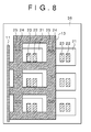
- FIG. 8 shows a configuration of an inverter device according to a third embodiment of the present invention from which a capacitor and a bus bar are removed, when seen from the above.
- the same parts as those in the first embodiment are labeled with the same reference signs.
- the configuration for three phases is shown in the third embodiment of the present invention, whereas the configuration for one phase is shown in the first embodiment.
- the use of the wiring conductor plate 13 in which parts for three phases are integrated and laminated with insulation sheets therebetween can reduce the number of parts and the assembling steps.
- FIG. 9 shows a configuration of an inverter device according to a fourth embodiment of the present invention from which a capacitor and a bus bar are removed, when seen from the above.
- the same parts as those in the first embodiment of the present invention are labeled with the same reference signs.
- the fourth embodiment of the present invention shows a case in which the modules for three phases are arranged adjacent to each other.
- the wires in the wiring conductor plate 13 of the laminated structure with the insulation sheet between the laminations, from the gate control terminal 24 and the ground control terminal 25 to the first control substrate 11 are arranged outside the modules 21 for three phases.
- the cooler 36 on which the modules are mounted can be made as small as possible.
- the wire portion outside the modules can be bent at about 90 degrees in the outside of the modules 21. This can reduce the size of the inverter.
- it is possible to configure a gate driving circuit for driving a power module which can largely reduce the number of the assembling steps, can ensure the insulation property, and is excellent in noise resistance.
- FIG. 10 shows a configuration of an inverter device according to a fifth embodiment of the present invention from which a capacitor and a bus bar are removed, when seen from the above.
- the same parts as those in the first embodiment are labeled with the same reference signs.
- a capacitor 53 is mounted on the wiring conductor plate 13 of the laminated structure with the insulation sheet between the laminations. This capacitor 53 is added for adjusting a switching rate of an IGBT mounted in the power module 21 or preventing malfunction of the IGBT.
- FIG. 11 shows a cross section of the wiring conductor plate 13 of the laminated structure with the insulation sheet between the insulations according to the fifth embodiment of the present invention.
- the ground wire 42 is removed only at the gate control terminal 24.
- the gate wire 41 is removed only at the ground control terminal 25.
- a gate driving circuit for driving a power module can be configured which can largely reduce the number of assembling steps, can ensure the insulation property, and is excellent in noise resistance.
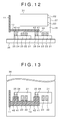
- FIG. 12 shows a configuration of an inverter device according to a sixth embodiment of the present invention, when seen from the side.
- FIG. 13 shows the configuration of the inverter device according to the sixth embodiment of the present invention from which a capacitor and a bus bar are removed, when seen from the above.
- Those diagrams show an inverter for one phase, although inverters are provided for three phases, respectively.
- the wiring conductor plate 13 of the laminated structure with the insulation sheet between the laminations is arranged at an upper level than the high-voltage main terminal 22 and the ground main terminal 23 of the power module.
- FIG. 14 is a perspective view of the wiring conductor plate 13 of the laminated structure with the insulation sheet between the laminations according to the sixth embodiment of the present invention.
- conductor plates respectively constituting the gate wire 41 and the ground wire 42 are bent. Because the wiring conductor plate 13 subjected to the above bending is used and arranged at an upper level than the high-voltage main terminal 22 and the ground main terminal 23 of the power module, the wires from the gate control terminal 24 and the ground control terminal 25 to the first control substrate 11 can be reduced to be minimum.
- a gate driving circuit for driving a power module can be configured which can largely reduce the number of assembling steps, can ensure the insulation property, and is excellent in noise resistance.
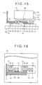
- FIG. 15 shows a configuration of an inverter device according to a seventh embodiment of the present invention, when seen from the side.
- FIG. 16 shows the configuration of the inverter device according to the seventh embodiment of the present invention from which a capacitor and a bus bar are removed, when seen from the above.
- Those diagrams show an inverter for one phase, although inverters are provided for three phases, respectively.
- a second control substrate 12 is connected to the gate control terminal 24 and the ground control terminal 25 of the power module.
- a gate resistance, and a capacitor and a Zener diode between the gate control terminal and the ground control terminal are mounted.
- the first control substrate 11 has the signal input portion, the logic portion, and the protection circuit portion which are mounted therein.
- a gate driving circuit for driving a power module can be configured which can largely reduce the number of assembling steps, can ensure the insulation property, and is excellent in noise resistance.
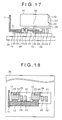
- FIG. 17 shows a configuration of an inverter device according to an eighth embodiment of the present invention, when seen from the side.
- FIG. 18 shows the configuration of the inverter device according to the eighth embodiment of the present invention from which a capacitor and a bus bar are removed, when seen from the above.
- Those diagrams show an inverter for one phase, although inverters are provided for three phases, respectively.
- the same parts as those in the first and seventh embodiments are labeled with the same reference signs.
- a high-voltage detection terminal 26 is provided.
- the second control substrate 12 is connected to the gate control terminal 24, the ground control terminal 25 of the power module, and the high-voltage detection terminal 26 of the power module.
- a gate resistance, a capacitor and a Zener diode both arranged between the gate control terminal and the ground control terminal, and a high-voltage diode, a resistance, and a capacitor which are provided between the high-voltage detection terminal and the ground control terminal are mounted.
- a voltage of the high-voltage detection terminal 26 of the power module is made the same potential as that of a ground control power supply of the power module by the high-voltage diode, the resistance, and the capacitor.
- a feature of the present invention is to use a conductor plate in which the gate wire, the ground wire, and a high-voltage detection wire are laminated, as wires connecting the control substrate 12 connected to the power module and the control substrate 11 in which the signal input portion, the power input portion, the logic portion, and the protection circuit are mounted, to each other.
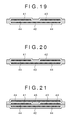
- FIG. 19 shows a cross section of the wiring conductor plate 13 of the laminated structure according to the eighth embodiment of the present invention.
- the gate wire 41 and the high-voltage detection wire 43 are arranged to be adjacent to each other. Between them, an insulation distance and a creepage distance can be ensured by a distance of several millimeters.
- the gate wire 41 and the high-voltage detection wire 43 are arranged such that the insulation sheet 44 is sandwiched between the gate wire 41 and the high-voltage detection wire 43, and the ground wire 42. Also, the insulation sheets 44 are arranged outside the gate wire 41, the high-voltage detection wire 43, and the ground wire 42 to sandwich them between the insulation sheets 44.
- a gate driving circuit for driving a power module can be configured which can largely reduce the number of assembling steps, can ensure the insulation property, and is excellent in noise resistance.
- FIG. 20 shows a cross section of the wiring conductor plate 13 of the laminated structure according to a ninth embodiment of the present invention.
- This embodiment is different from the eighth embodiment in that a detection voltage that is a high voltage is transmitted from the second control substrate 12 to the first control substrate 11. Since the high-voltage detection wire 43 is set to have a high potential, the gate wire 41 and the ground wire 42 are arranged to be adjacent to each other. Between them, an insulation distance and a creepage distance can be ensured by a distance of several millimeters.
- the gate wire 41 and the ground wire 42 are arranged such that the insulation sheet 44 is sandwiched between the gate wire 41 and the ground wire 42, and the high-voltage detection wire 43.
- a gate driving circuit for driving a power module can be configured which can largely reduce the number of assembling steps, can ensure the insulation property, and is excellent in noise resistance.
- FIG. 21 shows a cross section of the wiring conductor plate 13 of the laminated structure according to the tenth embodiment of the present invention.
- the tenth embodiment is different from the eighth embodiment in that a control power supply of the first substrate is transmitted from the first control substrate 11 to the second control substrate 12.
- the control power supply is set in a range between +15 V and +20 V.
- the gate wire 41 and the high-voltage detection wire 43 are arranged to be adjacent to each other. Between them, an insulation distance and a creepage distance can be ensured by a distance of several millimeters.
- the gate wire 41 and the high-voltage detection wire 43 are arranged such that the insulation sheet 44 is sandwiched between the gate wire 41 and the high-voltage detection wire 43, and the ground wire 42 and is also sandwiched between the gate wire 41 and the high-voltage detection wire 43, and a control power-supply wire 45. Since the configuration is employed in which the gate wire 41 and the high-voltage detection wire 43 are sandwiched between the ground wire 42 and the control power-supply wire 45, a gate driving circuit for driving a power module can be configured which is extremely excellent in noise resistance.
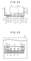
- FIG. 22 shows a configuration of an inverter device according to an eleventh embodiment of the present invention, when seen from the side.
- FIG. 23 shows the configuration of the inverter device according to the eleventh embodiment of the present invention from which a capacitor and a bus bar are removed, when seen from the above.
- Both drawings show the inverter device for one phase although the inverter devices are provided for three phases, respectively.
- a 2in1 type power module 27 in which IGBTs for two arms are mounted in one module is used.
- the 2in1 type power module 27 is mounted on the cooler 36. On the central portion of the power module 27, the high-voltage main terminal 22, the ground main terminal 23, and an output terminal 28 of the power module are provided.
- the power main circuit wire 37 which connects from the power terminal 32 of the capacitor and the high-voltage main terminal 22 of the power module and the ground main circuit wire 38 which connects the ground terminal 33 of the capacitor to the ground terminal 23 of the power module are made as short as possible, and those wires are arranged to be adjacent to each other.
- FIG. 5 also shows the cross section of the wiring conductor plate 13 of the laminated structure with the insulation sheet between the laminations according to the eleventh embodiment of the present invention, around the first control substrate.
- both the gate wire and the ground wire for the upper arm and those for the lower arm exist near the first control substrate.
- the gate wire 41 and the ground wire 42 for the upper arm are laminated with the insulation sheet 44 therebetween
- the gate wire 41 and the ground wire 42 for the lower arm are laminated with the insulation sheet 44 therebetween, and a predetermined insulation distance is ensured between the upper arm and the lower arm.
- a gate driving circuit for driving a power module can be configured which can largely reduce the number of assembling steps, can ensure the insulation property, and is excellent in noise resistance.
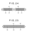
- FIG. 24 shows a cross section of the conductor plate 13 of the laminated structure according to a twelfth embodiment of the present invention.
- the same components as those in the first embodiment are labeled with the same reference signs.
- the gate wire 41 and the ground wire 42 for the lower arm IGBT are arranged in one side to be adjacent to each other and to sandwich the insulation sheet 44 therebetween.
- a gate driving circuit for driving a power module can be configured which can largely reduce the number of assembling steps, can ensure the insulation property, and is excellent in noise resistance.
- FIG. 25 shows a cross section of a printed board 46 according to a thirteenth embodiment of the present invention.
- the gate wire 41 and the ground wire 42 are arranged on an upper surface and a lower surface of the printed board 46, respectively.
- an insulation coating 47 is applied on the printed board 46.
- a gate driving circuit for driving a power module can be configured which can largely reduce the number of assembling steps, can ensure the insulation property, and is excellent in noise resistance.
Landscapes
- Engineering & Computer Science (AREA)
- Power Engineering (AREA)
- Inverter Devices (AREA)
- Electric Propulsion And Braking For Vehicles (AREA)
Abstract
Description
- The present invention relates to a power converting device and a railway vehicle mounted with the same and in particular to a mounting structure of a gate driving circuit for driving a power module of a high voltage, large current power converting device.
- In an inverter for converting a direct-current power to an alternating-current power and a converter for converting an alternating-current power to a direct-current power, a power module such as IGBT has been widely used. This power module is driven by a PWM signal from a microcomputer or the like mounted in a control logic portion of a converting portion via ON and OFF signals of a gate driving circuit. A portion which sends a signal from this gate driving circuit to the power module is a gate wire.
- There is a gate wiring technique using a two-level structure in which a power device is arranged at a lower level and a control substrate is arranged thereon, and a gate wire is connected with a pin structure, as described in Japanese Unexamined Patent Application Publication No.
Hei06 (1994)-45518 - A railway power converting device, a steel mill power converting device, and a wind power converting device use a power module with a withstand voltage of 1.7 kV or higher. In the power module with the withstand voltage of 1.7 kV or higher, main terminals thereof are arranged on a top surface thereof to be equally spaced from one another for ensuring a clearance insulation distance and a creepage insulation distance between terminals or from a heat sink of metal. Thus, a gate control terminal, a ground control terminal, and a high-voltage detection terminal are arranged in a small area of a portion relatively close to an end of the module. On the other hand, since a gate driving circuit for driving the power module includes a signal input portion, a power input portion, a logic portion, a protection circuit portion, and a gate resistance mounted therein, for example, the gate driving circuit is large and it is difficult to arrange it in an upper portion of the module.
- Moreover, for reducing the size of the inverter, power modules for three phases are arranged to be close to each other. Thus, the gate driving circuit is arranged to be away from the power modules. As a wiring technique for driving the power module, a technique is known in which a wire having insulation coating is used, as described in Japanese Unexamined Patent Application Publication No.
2007-185026 - As a wiring technique for driving the power module, a technique has been proposed in which conductor substrates are used as a gate-side wire and a cathode-side wire and are connected to each other with an insulation member therebetween, as described in Japanese Unexamined Patent Application Publication No.
Sho61(1986)-227661 - A railway power converting device, a steel mill power converting device, and a wind power converting device use a power module with a withstand voltage of 1.7 kV or higher, as described before. Moreover, for reducing the size of the inverter, the power modules are arranged to be close to each other, and the gate wire with the insulation coating for high-voltage application is used, as described in Japanese Unexamined Patent Application Publication No.
2007-185026 - In addition, Japanese Unexamined Patent Application Publication No.
Sho61(1986)-227661 - The present invention has been made in view of the above-described problems, and provides a gate driving circuit and a wiring structure which are excellent in assemblability and noise resistance and can ensure the insulation property.
- In order to address the above object, according to an aspect of the present invention, a power converting device is provided. The power converting device preferably includes: a power module having a high-voltage main terminal, a ground main terminal, and a gate control terminal and a ground control terminal for driving; a capacitor having a power terminal and a ground terminal; main circuit wires configured to connect main terminals of the power module and terminals of the capacitor, respectively; and a gate driving circuit configured to drive the power module. The gate driving circuit includes a first substrate in which a signal input portion, a power input portion, a logic portion, a protection circuit portion, and a gate driving portion are mounted. A gate-wire conductor plate and a ground-wire conductor plate which are laminated with an insulator arranged therebetween is arranged between the first substrate, and the gate control terminal and the ground terminal, and the insulator is provided on a surface of the gate-wire conductor plate and the ground-wire conductor plate.
- According to the present invention, a gate driving circuit and a wiring structure can be provided which are excellent in assemblability and noise resistance and can ensure the insulation property.
-
-
FIG. 1 shows a configuration of an inverter device according to a first embodiment, when seen from the side; -
FIG. 2 shows the configuration of the inverter device according to the first embodiment for one phase from which a capacitor and a bus bar are removed, when seen from the above; -
FIG. 3 shows a configuration of an inverter device of a conventional example for one phase from which a capacitor and a bus bar are removed, when seen from the above; -
FIG. 4 shows a cross section of a wiring conductor plate of a laminated structure with an insulation sheet between laminations according to the first embodiment, when cut near a control terminal portion; -
FIG. 5 shows a cross section of the wiring conductor plate of the laminated structure with the insulation sheet between the laminations according to the first embodiment, when cut near a first control substrate; -
FIG. 6 shows a cross section of a connecting portion between the wiring conductor plate of the laminated structure with the insulation sheet between the laminations according to the first embodiment and a control terminal of a power module; -
FIG. 7 shows a cross section of a connecting portion between a wiring conductor plate of a laminated structure with an insulation sheet between laminations according to a second embodiment and a control terminal of a power module; -
FIG. 8 shows a configuration of an inverter device according to a third embodiment in a case where three phases are integrated into one, from which a capacitor and a bus bar are removed, when seen from the above; -
FIG. 9 shows a configuration of an inverter device according to a fourth embodiment in a case where three phases are integrated into one, from which a capacitor and a bus bar are removed, when seen from the above; -
FIG. 10 shows a configuration of an inverter device according to a fifth embodiment from which a capacitor and a bus bar are removed, when seen from the above; -
FIG. 11 shows a cross section of a wiring conductor plate of a laminated structure with an insulation sheet between laminations according to the fifth embodiment; -
FIG. 12 shows a configuration of an inverter device according to a sixth embodiment, when seen from the side; -
FIG. 13 shows a configuration of the inverter device according to the sixth embodiment for one phase from which a capacitor and a bus bar are removed, when seen from the above; -
FIG. 14 is a perspective view of a wiring conductor plate of a laminated structure with an insulation sheet between laminations according to the sixth embodiment of the present invention; -
FIG. 15 shows a configuration of an inverter device according to a seventh embodiment, when seen from the side; -
FIG. 16 shows the configuration of the inverter device according to the seventh embodiment for one phase from which a capacitor and a bus bar are removed, when seen from the above; -
FIG. 17 shows a configuration of an inverter device according to an eighth embodiment, when seen from the side; -
FIG. 18 shows the configuration of the inverter device according to the eighth embodiment for one phase from which a capacitor and a bus bar are removed, when seen from the above; -
FIG. 19 shows a cross section of a wiring conductor plate of a laminated structure according to the eighth embodiment; -
FIG. 20 shows a cross section of a wiring conductor plate of a laminated structure according to a ninth embodiment; -
FIG. 21 shows a cross section of a wiring conductor plate of a laminated structure according to a tenth embodiment; -
FIG. 22 shows a configuration of an inverter device according to an eleventh embodiment, when seen from the side; -
FIG. 23 shows the configuration of the inverter device according to the eleventh embodiment for one phase from which a capacitor and a bus bar are removed, when seen from the above; -
FIG. 24 shows a cross section of a wiring conductor plate of a laminated structure according to a twelfth embodiment; and -
FIG. 25 shows a wiring substrate using a printed board according to a thirteenth embodiment. - Embodiments of the present invention are described below, referring to the drawings.
-
FIG. 1 shows a configuration of an inverter device according to a first embodiment of the present invention, when seen from the side.FIG. 2 shows the configuration of the inverter device according to the first embodiment from which a capacitor and a bus bar are removed, when seen from the above. While inverters for three phases are provided, both the drawings correspond to one phase. -
FIG. 3 shows a conventional method for mounting a gate wire and a ground wire. In the conventional method, agate wire 16 and aground wire 17, both shielded for high voltage application, are used. This method can reduce an inductance by employing a stranded wire for a gate and an emitter, but has a problem of an increase in the number of assembling steps. - In the first embodiment of the present invention, a
power module 21 is mounted on a cooler 36. Thepower module 21 has a high-voltagemain terminal 22 and a groundmain terminal 23 on a central portion thereof. Acapacitor 31 is arranged near thepower module 21, and includes apower terminal 32 and aground terminal 33 of thecapacitor 31. For reducing a peak voltage at switching, a powermain circuit wire 37 connecting from thepower terminal 32 of the capacitor to the high-voltagemain terminal 22 of the power module and a groundmain circuit wire 38 connecting from theground terminal 33 of the capacitor to the groundmain terminal 23 of the power module are arranged to be as short as possible and to be adjacent to each other so that the inductance from the terminals of thecapacitor 31 to the main terminals of the power module. - In the first embodiment of the present invention, a
wiring conductor plate 13 of a laminated structure with an insulation sheet between laminations is arranged between afirst control substrate 11 in which a signal input portion, a power input portion, a logic portion, a protection circuit portion, and a gate driving portion are mounted, and agate control terminal 24 and aground control terminal 25 of the power module. The present invention uses a conductor board in which a gate wire and a ground wire are laminated, thereby enabling large reduction in the number of assembling steps. -
FIG. 4 shows a cross section of thewiring conductor plate 13 of the laminated structure with the insulation sheet between the laminations according to the first embodiment of the present invention, around the control terminals. Thegate wire 41 and theground wire 42 are arranged to sandwich aninsulation sheet 44 therebetween. Also, theinsulation sheets 44 are arranged outside thegate wire 41 and theground wire 42 to sandwich thewires insulation sheet 44 preferably has an insulation resistance of 100 MΩ or higher. The use of PET film composite material or Nomex sheet can provide an excellent insulation characteristic in a thickness of 0.5 mm or less. Moreover, lamination of thegate wire 41 and theground wire 42 with theinsulation sheet 44 arranged therebetween can largely reduce the wiring inductance of a gate circuit and can also reduce effects of an electric field by a current flowing through the main circuit wires. According to the present invention, a gate driving circuit can be configured which can largely reduce the number of assembling steps, can ensure the insulation property, and is excellent in noise resistance. -
FIG. 5 shows a cross section of thewiring conductor plate 13 of the laminated structure with the insulation sheet between the laminations according to the first embodiment of the present invention, around the first control substrate. Around the first control substrate, the gate wire and the ground wire for an upper arm and those for a lower arm are both arranged. In the first embodiment, thegate wire 41 and theground wire 42 for the upper arm are laminated with theinsulation sheet 44 arranged therebetween, thegate wire 41 and theground wire 42 for the lower arm are laminated with theinsulation sheet 44 arranged therebetween, and the upper arm and the lower arm are spaced away with a predetermined insulation distance ensured therebetween. -
FIG. 6 shows a cross section of a connecting portion connecting thewiring conductor plate 13 of the laminated structure with the insulation sheet between the laminations and thegate control terminal 24 and theground control terminal 25 of the power module to each other according to the first embodiment. Thewiring conductor plate 13 of the laminated structure with the insulation sheet between the laminations is arranged such that the laminated structure extends near thegate control terminal 24 and theground control terminal 25 of the power module. Theground wire 42 at thegate control terminal 24 is removed, thegate wire 41 at theground control terminal 25 is removed, and thegate control terminal 24 and theground control terminal 25 are connected to thegate wire 41 and theground wire 42 byscrews 51, respectively. By employing this structure, the wiring inductance of the gate circuit can be largely reduced and it is possible to ensure sufficient reliability of insulation in the connecting portion. - Also in a case where MOSFET is used as a power device constituting the power module in the present invention, other than IGBT, the effects can be obtained. Moreover, the use of a SiC (silicon carbide) diode or SiCMOS transistor can result in further reduction in the size. Any insulator may be used as the insulation sheet in the present invention as long as it provides the insulation property, and the shape of the insulator is not limited to the sheet shape. Furthermore, the "high voltage" in the present invention preferably means to have a withstand voltage of 1200 V or higher, particularly 1.7 kV or higher. In this case, the effects of the present invention can be enhanced.
-
FIG. 7 shows a cross section of the connecting portion connecting thewiring conductor plate 13 of the laminated structure with the insulation sheet between laminations according to a second embodiment of the present invention and thegate control terminal 24 and theground control module 25 of the power module to each other. The same parts as those in the first embodiment are labeled with the same reference signs. - The
wiring conductor plate 13 has the laminated structure extending near thegate control terminal 24 and theground control terminal 25 of the power module. Theground wire 42 is removed only at thegate control terminal 24, and thegate wire 41 is removed only at theground control terminal 25. In connection of thegate control terminal 24 and thegate wire 41 to each other, the height is adjusted by means of aboss 52. With thescrews 51, thegate control terminal 24 and thegate wire 41 are connected to each other and theground control terminal 25 and theground wire 42 are connected to each other. By employing this structure, it is possible to largely reduce the wiring inductance of the gate circuit and ensure a sufficient level of reliability of insulation in the connecting portion. -
FIG. 8 shows a configuration of an inverter device according to a third embodiment of the present invention from which a capacitor and a bus bar are removed, when seen from the above. The same parts as those in the first embodiment are labeled with the same reference signs. - The configuration for three phases is shown in the third embodiment of the present invention, whereas the configuration for one phase is shown in the first embodiment. The use of the
wiring conductor plate 13 in which parts for three phases are integrated and laminated with insulation sheets therebetween can reduce the number of parts and the assembling steps. According to the present invention, it is possible to configure a gate driving circuit for driving a power module, which can largely reduce the number of the assembling steps, can ensure the insulation property, and is excellent in noise resistance. -
FIG. 9 shows a configuration of an inverter device according to a fourth embodiment of the present invention from which a capacitor and a bus bar are removed, when seen from the above. The same parts as those in the first embodiment of the present invention are labeled with the same reference signs. - The fourth embodiment of the present invention shows a case in which the modules for three phases are arranged adjacent to each other. The wires in the
wiring conductor plate 13 of the laminated structure with the insulation sheet between the laminations, from thegate control terminal 24 and theground control terminal 25 to thefirst control substrate 11 are arranged outside themodules 21 for three phases. By employing this method, the cooler 36 on which the modules are mounted can be made as small as possible. Moreover, the wire portion outside the modules can be bent at about 90 degrees in the outside of themodules 21. This can reduce the size of the inverter. According to the present invention, it is possible to configure a gate driving circuit for driving a power module, which can largely reduce the number of the assembling steps, can ensure the insulation property, and is excellent in noise resistance. -
FIG. 10 shows a configuration of an inverter device according to a fifth embodiment of the present invention from which a capacitor and a bus bar are removed, when seen from the above. The same parts as those in the first embodiment are labeled with the same reference signs. - In the fifth embodiment of the present invention, a
capacitor 53 is mounted on thewiring conductor plate 13 of the laminated structure with the insulation sheet between the laminations. Thiscapacitor 53 is added for adjusting a switching rate of an IGBT mounted in thepower module 21 or preventing malfunction of the IGBT. -
FIG. 11 shows a cross section of thewiring conductor plate 13 of the laminated structure with the insulation sheet between the insulations according to the fifth embodiment of the present invention. For the cathode of thecapacitor 53, theground wire 42 is removed only at thegate control terminal 24. For the anode of thecapacitor 53, thegate wire 41 is removed only at theground control terminal 25. According to the present invention, a gate driving circuit for driving a power module can be configured which can largely reduce the number of assembling steps, can ensure the insulation property, and is excellent in noise resistance. -
FIG. 12 shows a configuration of an inverter device according to a sixth embodiment of the present invention, when seen from the side.FIG. 13 shows the configuration of the inverter device according to the sixth embodiment of the present invention from which a capacitor and a bus bar are removed, when seen from the above. Those diagrams show an inverter for one phase, although inverters are provided for three phases, respectively. - The same parts as those in the first embodiment are labeled with the same reference signs. Unlike the first embodiment, the
wiring conductor plate 13 of the laminated structure with the insulation sheet between the laminations is arranged at an upper level than the high-voltagemain terminal 22 and the groundmain terminal 23 of the power module. By arranging thewiring conductor plate 13 of the laminated structure with the insulation sheet between the laminations at an upper level than the high-voltagemain terminal 22 and the groundmain terminal 23 of the power module, the wires from thegate control terminal 24 and theground control terminal 25 to thefirst control substrate 11 can be further shortened. -
FIG. 14 is a perspective view of thewiring conductor plate 13 of the laminated structure with the insulation sheet between the laminations according to the sixth embodiment of the present invention. For connecting thewiring conductor plate 13 of the laminated structure with the insulation sheet between the laminations to thegate control terminal 24 and theground control terminal 25, conductor plates respectively constituting thegate wire 41 and theground wire 42 are bent. Because thewiring conductor plate 13 subjected to the above bending is used and arranged at an upper level than the high-voltagemain terminal 22 and the groundmain terminal 23 of the power module, the wires from thegate control terminal 24 and theground control terminal 25 to thefirst control substrate 11 can be reduced to be minimum. According to the present invention, a gate driving circuit for driving a power module can be configured which can largely reduce the number of assembling steps, can ensure the insulation property, and is excellent in noise resistance. -
FIG. 15 shows a configuration of an inverter device according to a seventh embodiment of the present invention, when seen from the side.FIG. 16 shows the configuration of the inverter device according to the seventh embodiment of the present invention from which a capacitor and a bus bar are removed, when seen from the above. Those diagrams show an inverter for one phase, although inverters are provided for three phases, respectively. - The same parts as those in the first embodiment are labeled with the same reference signs. In the seventh embodiment of the present invention, a
second control substrate 12 is connected to thegate control terminal 24 and theground control terminal 25 of the power module. In thesecond control substrate 12, a gate resistance, and a capacitor and a Zener diode between the gate control terminal and the ground control terminal are mounted. Thefirst control substrate 11 has the signal input portion, the logic portion, and the protection circuit portion which are mounted therein. - Arranging the gate resistance, the capacitor, and Zener diode near the module enables a gate voltage of a power device in the power module to be further stabilized. A gate driving circuit for driving a power module can be configured which can largely reduce the number of assembling steps, can ensure the insulation property, and is excellent in noise resistance.
-
FIG. 17 shows a configuration of an inverter device according to an eighth embodiment of the present invention, when seen from the side.FIG. 18 shows the configuration of the inverter device according to the eighth embodiment of the present invention from which a capacitor and a bus bar are removed, when seen from the above. Those diagrams show an inverter for one phase, although inverters are provided for three phases, respectively. The same parts as those in the first and seventh embodiments are labeled with the same reference signs. - In this embodiment, a high-
voltage detection terminal 26 is provided. - The
second control substrate 12 is connected to thegate control terminal 24, theground control terminal 25 of the power module, and the high-voltage detection terminal 26 of the power module. In thesecond control substrate 12, a gate resistance, a capacitor and a Zener diode both arranged between the gate control terminal and the ground control terminal, and a high-voltage diode, a resistance, and a capacitor which are provided between the high-voltage detection terminal and the ground control terminal are mounted. A voltage of the high-voltage detection terminal 26 of the power module is made the same potential as that of a ground control power supply of the power module by the high-voltage diode, the resistance, and the capacitor. A feature of the present invention is to use a conductor plate in which the gate wire, the ground wire, and a high-voltage detection wire are laminated, as wires connecting thecontrol substrate 12 connected to the power module and thecontrol substrate 11 in which the signal input portion, the power input portion, the logic portion, and the protection circuit are mounted, to each other. -
FIG. 19 shows a cross section of thewiring conductor plate 13 of the laminated structure according to the eighth embodiment of the present invention. Since the high-voltage detection wire 43 is set to have the same potential as the ground control power supply, as described above, thegate wire 41 and the high-voltage detection wire 43 are arranged to be adjacent to each other. Between them, an insulation distance and a creepage distance can be ensured by a distance of several millimeters. Thegate wire 41 and the high-voltage detection wire 43 are arranged such that theinsulation sheet 44 is sandwiched between thegate wire 41 and the high-voltage detection wire 43, and theground wire 42. Also, theinsulation sheets 44 are arranged outside thegate wire 41, the high-voltage detection wire 43, and theground wire 42 to sandwich them between theinsulation sheets 44. According to the present invention, a gate driving circuit for driving a power module can be configured which can largely reduce the number of assembling steps, can ensure the insulation property, and is excellent in noise resistance. -
FIG. 20 shows a cross section of thewiring conductor plate 13 of the laminated structure according to a ninth embodiment of the present invention. This embodiment is different from the eighth embodiment in that a detection voltage that is a high voltage is transmitted from thesecond control substrate 12 to thefirst control substrate 11. Since the high-voltage detection wire 43 is set to have a high potential, thegate wire 41 and theground wire 42 are arranged to be adjacent to each other. Between them, an insulation distance and a creepage distance can be ensured by a distance of several millimeters. Thegate wire 41 and theground wire 42 are arranged such that theinsulation sheet 44 is sandwiched between thegate wire 41 and theground wire 42, and the high-voltage detection wire 43. Also, theinsulation sheets 44 are arranged outside thegate wire 41, theground wire 42, and the high-voltage detection wire 43 to sandwich them between theinsulation sheets 44. According to the present invention, a gate driving circuit for driving a power module can be configured which can largely reduce the number of assembling steps, can ensure the insulation property, and is excellent in noise resistance. -
FIG. 21 shows a cross section of thewiring conductor plate 13 of the laminated structure according to the tenth embodiment of the present invention. The tenth embodiment is different from the eighth embodiment in that a control power supply of the first substrate is transmitted from thefirst control substrate 11 to thesecond control substrate 12. The control power supply is set in a range between +15 V and +20 V. Thegate wire 41 and the high-voltage detection wire 43 are arranged to be adjacent to each other. Between them, an insulation distance and a creepage distance can be ensured by a distance of several millimeters. Thegate wire 41 and the high-voltage detection wire 43 are arranged such that theinsulation sheet 44 is sandwiched between thegate wire 41 and the high-voltage detection wire 43, and theground wire 42 and is also sandwiched between thegate wire 41 and the high-voltage detection wire 43, and a control power-supply wire 45. Since the configuration is employed in which thegate wire 41 and the high-voltage detection wire 43 are sandwiched between theground wire 42 and the control power-supply wire 45, a gate driving circuit for driving a power module can be configured which is extremely excellent in noise resistance. -
FIG. 22 shows a configuration of an inverter device according to an eleventh embodiment of the present invention, when seen from the side.FIG. 23 shows the configuration of the inverter device according to the eleventh embodiment of the present invention from which a capacitor and a bus bar are removed, when seen from the above. Both drawings show the inverter device for one phase although the inverter devices are provided for three phases, respectively. In this embodiment, a 2in1type power module 27 in which IGBTs for two arms are mounted in one module is used. - The 2in1
type power module 27 is mounted on the cooler 36. On the central portion of thepower module 27, the high-voltagemain terminal 22, the groundmain terminal 23, and anoutput terminal 28 of the power module are provided. The powermain circuit wire 37 which connects from thepower terminal 32 of the capacitor and the high-voltagemain terminal 22 of the power module and the groundmain circuit wire 38 which connects theground terminal 33 of the capacitor to theground terminal 23 of the power module are made as short as possible, and those wires are arranged to be adjacent to each other. -
FIG. 5 also shows the cross section of thewiring conductor plate 13 of the laminated structure with the insulation sheet between the laminations according to the eleventh embodiment of the present invention, around the first control substrate. As described in connection withFIG. 5 , both the gate wire and the ground wire for the upper arm and those for the lower arm exist near the first control substrate. In the eleventh embodiment, thegate wire 41 and theground wire 42 for the upper arm are laminated with theinsulation sheet 44 therebetween, thegate wire 41 and theground wire 42 for the lower arm are laminated with theinsulation sheet 44 therebetween, and a predetermined insulation distance is ensured between the upper arm and the lower arm. According to the present invention, a gate driving circuit for driving a power module can be configured which can largely reduce the number of assembling steps, can ensure the insulation property, and is excellent in noise resistance. -
FIG. 24 shows a cross section of theconductor plate 13 of the laminated structure according to a twelfth embodiment of the present invention. The same components as those in the first embodiment are labeled with the same reference signs. Thegate wire 41 and theground wire 42 for the lower arm IGBT are arranged in one side to be adjacent to each other and to sandwich theinsulation sheet 44 therebetween. According to the present invention, a gate driving circuit for driving a power module can be configured which can largely reduce the number of assembling steps, can ensure the insulation property, and is excellent in noise resistance. -
FIG. 25 shows a cross section of a printedboard 46 according to a thirteenth embodiment of the present invention. In a case where the printedboard 46 is used, thegate wire 41 and theground wire 42 are arranged on an upper surface and a lower surface of the printedboard 46, respectively. On the printedboard 46, aninsulation coating 47 is applied. According to the present invention, a gate driving circuit for driving a power module can be configured which can largely reduce the number of assembling steps, can ensure the insulation property, and is excellent in noise resistance.
Claims (15)
- A power converting device comprising:a power module having a high-voltage main terminal, a ground main terminal, and a gate control terminal and a ground control terminal for driving;a capacitor having a power terminal and a ground terminal;main circuit wires configured to connect main terminals of the power module and terminals of the capacitor, respectively; anda gate driving circuit configured to drive the power module,wherein the gate driving circuit includes a first substrate in which a signal input portion, a power input portion, a logic portion, a protection circuit portion, and a gate driving portion are mounted,a gate-wire conductor plate and a ground-wire conductor plate which are laminated via an insulator to form a laminated structure are provided between the first substrate and the gate control terminal and the ground control terminal, andthe insulator is provided on a surface of the gate-wire conductor plate and a surface of the ground-wire conductor plate.
- The power converting device according to claim 1, further comprising an electronic part provided on the laminated structure of the gate-wire conductor plate and the ground-wire conductor plate.
- The power converting device according to claim 1,
wherein the gate driving circuit includes a second substrate with an electronic part mounted therein,
the laminated structure of the gate-wire conductor plate and the ground-wire conductor plate is arranged between the first substrate and the second substrate via the insulator, and
the insulator is provided on the surface of the gate-wire conductor plate and the surface of the ground-wire conductor plate. - The power converting device according to claim 2 or 3, wherein the electronic part is one of a resistance, a capacitor, and a Zener diode.
- The power converting device according to any one of claims 1 to 4,
wherein a wire width of the gate-wire conductor plate and the ground-wire conductor plate is 3 mm or more. - A power converting device comprising:a power module having a high-voltage main terminal, a ground main terminal, a gate control terminal and a ground control terminal for driving, and a high-voltage detection terminal;a capacitor having a power terminal and a ground terminal;main circuit wires configured to connect main terminals of the power module and terminals of the capacitor, respectively; anda gate driving circuit configured to drive the power module, whereinthe gate driving circuit includes a first substrate in which a signal input portion, a power input portion, a logic portion, a protection circuit portion, and a gate driving portion are mounted,a gate-wire conductor plate, a ground-wire conductor plate, and a high-voltage detection wire conductor plate which are laminated with an insulator arranged therebetween to form a laminated structure is arranged between the first substrate and each of the gate control terminal, the ground control terminal, and the high-voltage detection terminal, andthe insulator is provided on surfaces of the laminated structure of the conductor plates.
- The power converting device according to claim 6, further comprising an electronic part provided on the laminated structure of the conductor plates.
- The power converting device according to claim 6,
wherein the gate driving circuit includes a second substrate with an electronic part mounted therein, and
the laminated structure of the gate-wire conductor plate, the ground-wire conductor plate, and the high-voltage detection wire conductor plate is arranged between the first substrate and the second substrate via the insulator, and
the insulator is provided on the surfaces of the laminated structure of the conductor plates. - The power converting device according to claim 7 or 8,
wherein the electronic part is one of a resistance, a capacitor, and a Zener diode. - The power converting device according to any one of claims 6 to 9,
wherein a wire width of the gate-wire conductor plate and the ground-wire conductor plate is 3 mm or more. - The power converting device according to claim 6, wherein the gate driving circuit includes a second substrate in which a gate resistance of a power device, an input capacitor, a Zener diode, a high-voltage diode, and an output buffer circuit are mounted, and
the gate-wire conductor plate, the ground-wire conductor plate, the high-voltage detection wire conductor plate, and one or more types of control power wire conductor plates which are laminated via the insulator to form the laminated structure are provided, and the insulator is provided on a surface of each of the conductor plates. - The power converting device according to any one of claims 1, 2, 3, 6, 7, and 8,
wherein the conductor plates for a plurality of phases are integrated into one. - The power converting device according to any one of claims 1, 2, and 3,
wherein the gate driving circuit includes a printed board between the first substrate, and the gate control terminal and the ground control terminal, and
the printed board is subjected to insulation treatment. - The power converting device according to any one of claims 1 to 13, wherein the power module incudes a SiC diode or a SiC-MOSFET.
- A railway vehicle mounted with the power converting device according to any one of claims 1 to 14.
Applications Claiming Priority (1)
| Application Number | Priority Date | Filing Date | Title |
|---|---|---|---|
| JP2014076621A JP6230946B2 (en) | 2014-04-03 | 2014-04-03 | Power conversion device and railway vehicle equipped with the same |
Publications (2)
| Publication Number | Publication Date |
|---|---|
| EP2928057A1 true EP2928057A1 (en) | 2015-10-07 |
| EP2928057B1 EP2928057B1 (en) | 2022-07-13 |
Family
ID=52440537
Family Applications (1)
| Application Number | Title | Priority Date | Filing Date |
|---|---|---|---|
| EP15150223.4A Active EP2928057B1 (en) | 2014-04-03 | 2015-01-06 | Power converting device and railway vehicle mounted with the same |
Country Status (3)
| Country | Link |
|---|---|
| EP (1) | EP2928057B1 (en) |
| JP (1) | JP6230946B2 (en) |
| CN (1) | CN104980004B (en) |
Cited By (4)
| Publication number | Priority date | Publication date | Assignee | Title |
|---|---|---|---|---|
| US10381945B2 (en) | 2016-10-07 | 2019-08-13 | Fuji Electric Co., Ltd. | Gate driving apparatus |
| EP3664274A4 (en) * | 2017-08-03 | 2021-03-31 | Hitachi, Ltd. | CURRENT CONVERSION DEVICE AND VEHICLE EQUIPPED WITH CURRENT CONVERSION DEVICE |
| EP3667892A4 (en) * | 2017-08-09 | 2021-04-07 | Hitachi, Ltd. | POWER CONVERSION DEVICE AND ASSOCIATED COOLING PROCESS |
| US12336094B2 (en) | 2022-01-31 | 2025-06-17 | Fuji Electric Co., Ltd. | Wiring board and power conversion apparatus |
Families Citing this family (4)
| Publication number | Priority date | Publication date | Assignee | Title |
|---|---|---|---|---|
| JP6720601B2 (en) | 2016-03-16 | 2020-07-08 | 富士電機株式会社 | Power converter |
| JP6103122B1 (en) | 2016-08-17 | 2017-03-29 | 富士電機株式会社 | Signal relay board for power semiconductor modules |
| JP6749428B2 (en) * | 2017-01-31 | 2020-09-02 | 株式会社日立製作所 | Power converter |
| EP3678287B1 (en) | 2017-08-30 | 2023-11-22 | Hitachi, Ltd. | Power conversion device and power conversion method |
Citations (7)
| Publication number | Priority date | Publication date | Assignee | Title |
|---|---|---|---|---|
| JPS61227661A (en) | 1985-04-02 | 1986-10-09 | Fuji Electric Co Ltd | Parallel device of gate turn-off thyristors |
| JPH0645518A (en) | 1992-07-24 | 1994-02-18 | Fuji Electric Co Ltd | Power semiconductor device |
| JP2002142444A (en) * | 2000-11-07 | 2002-05-17 | Toshiba Corp | Power converter |
| JP2007185026A (en) | 2006-01-05 | 2007-07-19 | Hitachi Ltd | Power converter |
| US20110308834A1 (en) * | 2010-06-18 | 2011-12-22 | Fuji Electric Holdings Co., Ltd. | Laminated bus bar |
| US20120305283A1 (en) * | 2011-05-31 | 2012-12-06 | Tesla Motors, Inc. | Power electronics interconnection for electric motor drives |
| EP2675053A1 (en) * | 2011-02-10 | 2013-12-18 | Mitsubishi Electric Corporation | Power conversion device |
Family Cites Families (5)
| Publication number | Priority date | Publication date | Assignee | Title |
|---|---|---|---|---|
| JP2003303939A (en) * | 2002-04-08 | 2003-10-24 | Hitachi Ltd | Power semiconductor device and inverter device |
| JP4432913B2 (en) * | 2006-02-10 | 2010-03-17 | 株式会社デンソー | Laminated bus bar assembly and molding apparatus therefor |
| JP2008192808A (en) * | 2007-02-05 | 2008-08-21 | Murata Mfg Co Ltd | Mounting structure of multilayer electronic components |
| JP5171520B2 (en) * | 2008-09-30 | 2013-03-27 | 日立オートモティブシステムズ株式会社 | Power converter |
| JP5338639B2 (en) * | 2009-11-27 | 2013-11-13 | 株式会社デンソー | Power converter |
-
2014
- 2014-04-03 JP JP2014076621A patent/JP6230946B2/en active Active
-
2015
- 2015-01-06 EP EP15150223.4A patent/EP2928057B1/en active Active
- 2015-01-14 CN CN201510018393.3A patent/CN104980004B/en active Active
Patent Citations (7)
| Publication number | Priority date | Publication date | Assignee | Title |
|---|---|---|---|---|
| JPS61227661A (en) | 1985-04-02 | 1986-10-09 | Fuji Electric Co Ltd | Parallel device of gate turn-off thyristors |
| JPH0645518A (en) | 1992-07-24 | 1994-02-18 | Fuji Electric Co Ltd | Power semiconductor device |
| JP2002142444A (en) * | 2000-11-07 | 2002-05-17 | Toshiba Corp | Power converter |
| JP2007185026A (en) | 2006-01-05 | 2007-07-19 | Hitachi Ltd | Power converter |
| US20110308834A1 (en) * | 2010-06-18 | 2011-12-22 | Fuji Electric Holdings Co., Ltd. | Laminated bus bar |
| EP2675053A1 (en) * | 2011-02-10 | 2013-12-18 | Mitsubishi Electric Corporation | Power conversion device |
| US20120305283A1 (en) * | 2011-05-31 | 2012-12-06 | Tesla Motors, Inc. | Power electronics interconnection for electric motor drives |
Cited By (4)
| Publication number | Priority date | Publication date | Assignee | Title |
|---|---|---|---|---|
| US10381945B2 (en) | 2016-10-07 | 2019-08-13 | Fuji Electric Co., Ltd. | Gate driving apparatus |
| EP3664274A4 (en) * | 2017-08-03 | 2021-03-31 | Hitachi, Ltd. | CURRENT CONVERSION DEVICE AND VEHICLE EQUIPPED WITH CURRENT CONVERSION DEVICE |
| EP3667892A4 (en) * | 2017-08-09 | 2021-04-07 | Hitachi, Ltd. | POWER CONVERSION DEVICE AND ASSOCIATED COOLING PROCESS |
| US12336094B2 (en) | 2022-01-31 | 2025-06-17 | Fuji Electric Co., Ltd. | Wiring board and power conversion apparatus |
Also Published As
| Publication number | Publication date |
|---|---|
| JP2015198545A (en) | 2015-11-09 |
| EP2928057B1 (en) | 2022-07-13 |
| CN104980004B (en) | 2017-08-08 |
| JP6230946B2 (en) | 2017-11-15 |
| CN104980004A (en) | 2015-10-14 |
Similar Documents
| Publication | Publication Date | Title |
|---|---|---|
| EP2928057A1 (en) | Power converting device and railway vehicle mounted with the same | |
| US10134718B2 (en) | Power semiconductor module | |
| US10153708B2 (en) | Three-level power converter | |
| EP2811642A1 (en) | Power converter and method for manufacturing power converter | |
| US20130056755A1 (en) | Power semiconductor module | |
| CN105874596A (en) | Semiconductor module | |
| JP2018130015A (en) | Low inductive half-bridge device | |
| CN110622307B (en) | Semiconductor module and power conversion device | |
| CN103650316A (en) | Power conversion device | |
| CN110168899B (en) | Power conversion device | |
| CN103597726A (en) | Power converter | |
| CN103597728A (en) | Power conversion device | |
| CN103650317A (en) | Power conversion device | |
| US10418893B2 (en) | Fast-switching circuit assembly for a converter | |
| CN106663676A (en) | Semiconductor device and multiphase semiconductor device | |
| CN102484110A (en) | Power semiconductor module | |
| CN104518681A (en) | Electric power conversion device | |
| US10381947B2 (en) | Power conversion apparatus | |
| JP6766965B2 (en) | Power converter | |
| CN104380587B (en) | Power conversion device | |
| JP2017005808A (en) | Power converter | |
| CN110506384B (en) | Low-Inductance Half-Bridge Power Modules | |
| CN106411107B (en) | Power inverter | |
| EP3168871B1 (en) | Semiconductor device and a method of making a semiconductor device | |
| JPWO2013105456A1 (en) | Circuit boards and electronic devices |
Legal Events
| Date | Code | Title | Description |
|---|---|---|---|
| PUAI | Public reference made under article 153(3) epc to a published international application that has entered the european phase |
Free format text: ORIGINAL CODE: 0009012 |
|
| 17P | Request for examination filed |
Effective date: 20150123 |
|
| AK | Designated contracting states |
Kind code of ref document: A1 Designated state(s): AL AT BE BG CH CY CZ DE DK EE ES FI FR GB GR HR HU IE IS IT LI LT LU LV MC MK MT NL NO PL PT RO RS SE SI SK SM TR |
|
| AX | Request for extension of the european patent |
Extension state: BA ME |
|
| STAA | Information on the status of an ep patent application or granted ep patent |
Free format text: STATUS: EXAMINATION IS IN PROGRESS |
|
| 17Q | First examination report despatched |
Effective date: 20170503 |
|
| GRAP | Despatch of communication of intention to grant a patent |
Free format text: ORIGINAL CODE: EPIDOSNIGR1 |
|
| STAA | Information on the status of an ep patent application or granted ep patent |
Free format text: STATUS: GRANT OF PATENT IS INTENDED |
|
| INTG | Intention to grant announced |
Effective date: 20220203 |
|
| GRAS | Grant fee paid |
Free format text: ORIGINAL CODE: EPIDOSNIGR3 |
|
| GRAA | (expected) grant |
Free format text: ORIGINAL CODE: 0009210 |
|
| STAA | Information on the status of an ep patent application or granted ep patent |
Free format text: STATUS: THE PATENT HAS BEEN GRANTED |
|
| AK | Designated contracting states |
Kind code of ref document: B1 Designated state(s): AL AT BE BG CH CY CZ DE DK EE ES FI FR GB GR HR HU IE IS IT LI LT LU LV MC MK MT NL NO PL PT RO RS SE SI SK SM TR |
|
| REG | Reference to a national code |
Ref country code: GB Ref legal event code: FG4D |
|
| REG | Reference to a national code |
Ref country code: CH Ref legal event code: EP |
|
| REG | Reference to a national code |
Ref country code: DE Ref legal event code: R096 Ref document number: 602015079834 Country of ref document: DE |
|
| REG | Reference to a national code |
Ref country code: IE Ref legal event code: FG4D |
|
| REG | Reference to a national code |
Ref country code: AT Ref legal event code: REF Ref document number: 1504784 Country of ref document: AT Kind code of ref document: T Effective date: 20220815 |
|
| REG | Reference to a national code |
Ref country code: LT Ref legal event code: MG9D |
|
| REG | Reference to a national code |
Ref country code: NL Ref legal event code: MP Effective date: 20220713 |
|
| PG25 | Lapsed in a contracting state [announced via postgrant information from national office to epo] |
Ref country code: SE Free format text: LAPSE BECAUSE OF FAILURE TO SUBMIT A TRANSLATION OF THE DESCRIPTION OR TO PAY THE FEE WITHIN THE PRESCRIBED TIME-LIMIT Effective date: 20220713 Ref country code: RS Free format text: LAPSE BECAUSE OF FAILURE TO SUBMIT A TRANSLATION OF THE DESCRIPTION OR TO PAY THE FEE WITHIN THE PRESCRIBED TIME-LIMIT Effective date: 20220713 Ref country code: PT Free format text: LAPSE BECAUSE OF FAILURE TO SUBMIT A TRANSLATION OF THE DESCRIPTION OR TO PAY THE FEE WITHIN THE PRESCRIBED TIME-LIMIT Effective date: 20221114 Ref country code: NO Free format text: LAPSE BECAUSE OF FAILURE TO SUBMIT A TRANSLATION OF THE DESCRIPTION OR TO PAY THE FEE WITHIN THE PRESCRIBED TIME-LIMIT Effective date: 20221013 Ref country code: NL Free format text: LAPSE BECAUSE OF FAILURE TO SUBMIT A TRANSLATION OF THE DESCRIPTION OR TO PAY THE FEE WITHIN THE PRESCRIBED TIME-LIMIT Effective date: 20220713 Ref country code: LV Free format text: LAPSE BECAUSE OF FAILURE TO SUBMIT A TRANSLATION OF THE DESCRIPTION OR TO PAY THE FEE WITHIN THE PRESCRIBED TIME-LIMIT Effective date: 20220713 Ref country code: LT Free format text: LAPSE BECAUSE OF FAILURE TO SUBMIT A TRANSLATION OF THE DESCRIPTION OR TO PAY THE FEE WITHIN THE PRESCRIBED TIME-LIMIT Effective date: 20220713 Ref country code: FI Free format text: LAPSE BECAUSE OF FAILURE TO SUBMIT A TRANSLATION OF THE DESCRIPTION OR TO PAY THE FEE WITHIN THE PRESCRIBED TIME-LIMIT Effective date: 20220713 Ref country code: ES Free format text: LAPSE BECAUSE OF FAILURE TO SUBMIT A TRANSLATION OF THE DESCRIPTION OR TO PAY THE FEE WITHIN THE PRESCRIBED TIME-LIMIT Effective date: 20220713 |
|
| REG | Reference to a national code |
Ref country code: AT Ref legal event code: MK05 Ref document number: 1504784 Country of ref document: AT Kind code of ref document: T Effective date: 20220713 |
|
| PG25 | Lapsed in a contracting state [announced via postgrant information from national office to epo] |
Ref country code: PL Free format text: LAPSE BECAUSE OF FAILURE TO SUBMIT A TRANSLATION OF THE DESCRIPTION OR TO PAY THE FEE WITHIN THE PRESCRIBED TIME-LIMIT Effective date: 20220713 Ref country code: IS Free format text: LAPSE BECAUSE OF FAILURE TO SUBMIT A TRANSLATION OF THE DESCRIPTION OR TO PAY THE FEE WITHIN THE PRESCRIBED TIME-LIMIT Effective date: 20221113 Ref country code: HR Free format text: LAPSE BECAUSE OF FAILURE TO SUBMIT A TRANSLATION OF THE DESCRIPTION OR TO PAY THE FEE WITHIN THE PRESCRIBED TIME-LIMIT Effective date: 20220713 Ref country code: GR Free format text: LAPSE BECAUSE OF FAILURE TO SUBMIT A TRANSLATION OF THE DESCRIPTION OR TO PAY THE FEE WITHIN THE PRESCRIBED TIME-LIMIT Effective date: 20221014 |
|
| REG | Reference to a national code |
Ref country code: DE Ref legal event code: R097 Ref document number: 602015079834 Country of ref document: DE |
|
| PG25 | Lapsed in a contracting state [announced via postgrant information from national office to epo] |
Ref country code: SM Free format text: LAPSE BECAUSE OF FAILURE TO SUBMIT A TRANSLATION OF THE DESCRIPTION OR TO PAY THE FEE WITHIN THE PRESCRIBED TIME-LIMIT Effective date: 20220713 Ref country code: RO Free format text: LAPSE BECAUSE OF FAILURE TO SUBMIT A TRANSLATION OF THE DESCRIPTION OR TO PAY THE FEE WITHIN THE PRESCRIBED TIME-LIMIT Effective date: 20220713 Ref country code: DK Free format text: LAPSE BECAUSE OF FAILURE TO SUBMIT A TRANSLATION OF THE DESCRIPTION OR TO PAY THE FEE WITHIN THE PRESCRIBED TIME-LIMIT Effective date: 20220713 Ref country code: CZ Free format text: LAPSE BECAUSE OF FAILURE TO SUBMIT A TRANSLATION OF THE DESCRIPTION OR TO PAY THE FEE WITHIN THE PRESCRIBED TIME-LIMIT Effective date: 20220713 Ref country code: AT Free format text: LAPSE BECAUSE OF FAILURE TO SUBMIT A TRANSLATION OF THE DESCRIPTION OR TO PAY THE FEE WITHIN THE PRESCRIBED TIME-LIMIT Effective date: 20220713 |
|
| PLBE | No opposition filed within time limit |
Free format text: ORIGINAL CODE: 0009261 |
|
| STAA | Information on the status of an ep patent application or granted ep patent |
Free format text: STATUS: NO OPPOSITION FILED WITHIN TIME LIMIT |
|
| PG25 | Lapsed in a contracting state [announced via postgrant information from national office to epo] |
Ref country code: SK Free format text: LAPSE BECAUSE OF FAILURE TO SUBMIT A TRANSLATION OF THE DESCRIPTION OR TO PAY THE FEE WITHIN THE PRESCRIBED TIME-LIMIT Effective date: 20220713 Ref country code: EE Free format text: LAPSE BECAUSE OF FAILURE TO SUBMIT A TRANSLATION OF THE DESCRIPTION OR TO PAY THE FEE WITHIN THE PRESCRIBED TIME-LIMIT Effective date: 20220713 |
|
| 26N | No opposition filed |
Effective date: 20230414 |
|
| PG25 | Lapsed in a contracting state [announced via postgrant information from national office to epo] |
Ref country code: AL Free format text: LAPSE BECAUSE OF FAILURE TO SUBMIT A TRANSLATION OF THE DESCRIPTION OR TO PAY THE FEE WITHIN THE PRESCRIBED TIME-LIMIT Effective date: 20220713 |
|
| PG25 | Lapsed in a contracting state [announced via postgrant information from national office to epo] |
Ref country code: SI Free format text: LAPSE BECAUSE OF FAILURE TO SUBMIT A TRANSLATION OF THE DESCRIPTION OR TO PAY THE FEE WITHIN THE PRESCRIBED TIME-LIMIT Effective date: 20220713 |
|
| REG | Reference to a national code |
Ref country code: CH Ref legal event code: PL |
|
| PG25 | Lapsed in a contracting state [announced via postgrant information from national office to epo] |
Ref country code: LU Free format text: LAPSE BECAUSE OF NON-PAYMENT OF DUE FEES Effective date: 20230106 |
|
| REG | Reference to a national code |
Ref country code: BE Ref legal event code: MM Effective date: 20230131 |
|
| PG25 | Lapsed in a contracting state [announced via postgrant information from national office to epo] |
Ref country code: LI Free format text: LAPSE BECAUSE OF NON-PAYMENT OF DUE FEES Effective date: 20230131 Ref country code: CH Free format text: LAPSE BECAUSE OF NON-PAYMENT OF DUE FEES Effective date: 20230131 |
|
| PG25 | Lapsed in a contracting state [announced via postgrant information from national office to epo] |
Ref country code: FR Free format text: LAPSE BECAUSE OF NON-PAYMENT OF DUE FEES Effective date: 20230131 Ref country code: BE Free format text: LAPSE BECAUSE OF NON-PAYMENT OF DUE FEES Effective date: 20230131 |
|
| PG25 | Lapsed in a contracting state [announced via postgrant information from national office to epo] |
Ref country code: IE Free format text: LAPSE BECAUSE OF NON-PAYMENT OF DUE FEES Effective date: 20230106 |
|
| PG25 | Lapsed in a contracting state [announced via postgrant information from national office to epo] |
Ref country code: MC Free format text: LAPSE BECAUSE OF FAILURE TO SUBMIT A TRANSLATION OF THE DESCRIPTION OR TO PAY THE FEE WITHIN THE PRESCRIBED TIME-LIMIT Effective date: 20220713 |
|
| PG25 | Lapsed in a contracting state [announced via postgrant information from national office to epo] |
Ref country code: MC Free format text: LAPSE BECAUSE OF FAILURE TO SUBMIT A TRANSLATION OF THE DESCRIPTION OR TO PAY THE FEE WITHIN THE PRESCRIBED TIME-LIMIT Effective date: 20220713 |
|
| PG25 | Lapsed in a contracting state [announced via postgrant information from national office to epo] |
Ref country code: BG Free format text: LAPSE BECAUSE OF FAILURE TO SUBMIT A TRANSLATION OF THE DESCRIPTION OR TO PAY THE FEE WITHIN THE PRESCRIBED TIME-LIMIT Effective date: 20220713 |
|
| PG25 | Lapsed in a contracting state [announced via postgrant information from national office to epo] |
Ref country code: BG Free format text: LAPSE BECAUSE OF FAILURE TO SUBMIT A TRANSLATION OF THE DESCRIPTION OR TO PAY THE FEE WITHIN THE PRESCRIBED TIME-LIMIT Effective date: 20220713 |
|
| PG25 | Lapsed in a contracting state [announced via postgrant information from national office to epo] |
Ref country code: CY Free format text: LAPSE BECAUSE OF FAILURE TO SUBMIT A TRANSLATION OF THE DESCRIPTION OR TO PAY THE FEE WITHIN THE PRESCRIBED TIME-LIMIT; INVALID AB INITIO Effective date: 20150106 |
|
| PG25 | Lapsed in a contracting state [announced via postgrant information from national office to epo] |
Ref country code: HU Free format text: LAPSE BECAUSE OF FAILURE TO SUBMIT A TRANSLATION OF THE DESCRIPTION OR TO PAY THE FEE WITHIN THE PRESCRIBED TIME-LIMIT; INVALID AB INITIO Effective date: 20150106 |
|
| PG25 | Lapsed in a contracting state [announced via postgrant information from national office to epo] |
Ref country code: TR Free format text: LAPSE BECAUSE OF FAILURE TO SUBMIT A TRANSLATION OF THE DESCRIPTION OR TO PAY THE FEE WITHIN THE PRESCRIBED TIME-LIMIT Effective date: 20220713 |
|
| PGFP | Annual fee paid to national office [announced via postgrant information from national office to epo] |
Ref country code: GB Payment date: 20251219 Year of fee payment: 12 |
|
| PGFP | Annual fee paid to national office [announced via postgrant information from national office to epo] |
Ref country code: DE Payment date: 20251217 Year of fee payment: 12 |
|
| PGFP | Annual fee paid to national office [announced via postgrant information from national office to epo] |
Ref country code: IT Payment date: 20260107 Year of fee payment: 12 |