EP2921882B1 - Reading device and method for measuring energy and flight time using silicon photomultipliers - Google Patents
Reading device and method for measuring energy and flight time using silicon photomultipliers Download PDFInfo
- Publication number
- EP2921882B1 EP2921882B1 EP13814664.2A EP13814664A EP2921882B1 EP 2921882 B1 EP2921882 B1 EP 2921882B1 EP 13814664 A EP13814664 A EP 13814664A EP 2921882 B1 EP2921882 B1 EP 2921882B1
- Authority
- EP
- European Patent Office
- Prior art keywords
- time
- threshold
- channel
- input
- input pulse
- Prior art date
- Legal status (The legal status is an assumption and is not a legal conclusion. Google has not performed a legal analysis and makes no representation as to the accuracy of the status listed.)
- Active
Links
Images

Classifications
-
- G—PHYSICS
- G01—MEASURING; TESTING
- G01T—MEASUREMENT OF NUCLEAR OR X-RADIATION
- G01T1/00—Measuring X-radiation, gamma radiation, corpuscular radiation, or cosmic radiation
- G01T1/16—Measuring radiation intensity
- G01T1/24—Measuring radiation intensity with semiconductor detectors
- G01T1/248—Silicon photomultipliers [SiPM], e.g. an avalanche photodiode [APD] array on a common Si substrate
-
- G—PHYSICS
- G01—MEASURING; TESTING
- G01T—MEASUREMENT OF NUCLEAR OR X-RADIATION
- G01T1/00—Measuring X-radiation, gamma radiation, corpuscular radiation, or cosmic radiation
- G01T1/16—Measuring radiation intensity
- G01T1/24—Measuring radiation intensity with semiconductor detectors
- G01T1/249—Measuring radiation intensity with semiconductor detectors specially adapted for use in SPECT or PET
-
- G—PHYSICS
- G01—MEASURING; TESTING
- G01T—MEASUREMENT OF NUCLEAR OR X-RADIATION
- G01T1/00—Measuring X-radiation, gamma radiation, corpuscular radiation, or cosmic radiation
- G01T1/29—Measurement performed on radiation beams, e.g. position or section of the beam; Measurement of spatial distribution of radiation
- G01T1/2914—Measurement of spatial distribution of radiation
- G01T1/2985—In depth localisation, e.g. using positron emitters; Tomographic imaging (longitudinal and transverse section imaging; apparatus for radiation diagnosis sequentially in different planes, steroscopic radiation diagnosis)
Definitions
- Time-of-flight information on PET systems allows for unprecedented sensitivity, as the signal-to-noise ratio and thus the background rejection are very much improved.
- the very high gain of the silicon multiplier (SiPM) and its sensitivity to single photon hits makes it a good candidate for highly compact systems.
- a timing resolution of 200 ps is enough to confine the event origin with a FWHM position uncertainty of 30 mm along the line-of-response (LOR). Achieving this fine resolution calls for fast front-end electronics, capable of extracting a very precise time stamp of each event.
- Scintillation light statistics which include intrinsic timing characteristics of the crystal and the travel path of the photons, along with the time drift inherent to the e-h pair generation of the SiPM, may become a source of jitter that could ultimately compromise the targeted time resolution.
- the signal shape fluctuation at the output of the photodetector reflects the statistical time distribution of each photon building up the signal. Since the arrival time of these photons is weakly correlated to the time of the electron-positron annihilation, the readout system must be able to trigger on the first photo-electron. This ability requires low-noise front-end electronics with enough bandwidth such that the time walk across the dynamic range becomes negligible.
- PTT detection module which specifically includes a readout apparatus for time-of flight and energy measurements, providing accurate time-of-flight information when used in PET systems with fast crystals, which comprises a silicon photomultiplier (SiPM) per channel, front end conditioning circuits which offer low input impedance and high bandwidth, and a time-to-digital converter based on time interpolation, per channel.
- SiPM silicon photomultiplier
- CMOS front-end electronics for SiPM read-out which comprise a preamplifier suitable for a large dynamic range and extremely fast rise time of the detector signal. It includes a current-mode solution, where the preamplifier exploits a current buffer with very low impedance that allows fast timing, high dynamic range and wide bandwidth.
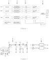
- Figure 1 the readout architecture in a multi-channel system, including in each channel amplification circuits (1) and discriminators (2) of the input signal; two Time-to-Digital Converter (TDC) based on analog time interpolation (3); a global controller of the readout of the time and energy digital data stored in each channel (4).
- TDC Time-to-Digital Converter
- Figure 2 the architecture of the amplification and discrimination of the input signal, including differential amplifiers of low impedance using a regulated gate cascade (5), with adjustable baseline of the input node (6) and a delay line at the low-threshold discriminator output (7).
- Figure 4 the preferred embodiment of the described readout method in a 64-channel ASIC, polarization and calibration blocks, and a global controller, where one edge (10) is free of pins, such that a twin chip rotated by 180° can be abutted to form a compact circuit with 128 channels.
- the present invention includes a readout apparatus according to appended claim 1 and a readout method according to appended claim 10.
- the readout apparatus for time-of-flight and energy measurements which forms this invention and which provides accurate time-of-flight information when used in PET systems with fast crystals (e.g. LYSO), which allow to confine the origin of the two 511 keV photons with a position uncertainty of 30 mm along the line-of-response (LOR), essentially includes:
- Said apparatus also comprises:
- the invention also relates to a readout method for time-of-flight and energy measurements with silicon photomultipliers, illustrated in Figure 3 , which is essentially characterized by front-end conditioning of input pulses with low impedance input differential amplifiers built-up by a regulated-gate cascode circuit with low-noise, high bandwidth and a power consumption smaller than 10 mW per channel, with the ability to fine tune the DC node voltage at the input, measuring the time-stamp of the input pulse using a low threshold, and measuring the energy of the input pulse through the time difference between the two time stamps, where the extraction of the time information is based on two voltage thresholds, used respectively in the pulse raising and falling edges, while the event validation is given by a higher voltage in the second threshold, the time stamps consisting of a coarse 10-bit data latched from the global gray-encoded coarse time counter, and a 8-bit fine time measurement derived from a 50 ps time binning time-to-digital converter, this fine time stamp being a direct measure
- a common feature of prior art designs is the use of a very power consuming front-end amplifier, in order to decrease the input impedance of the said circuit and hence achieve high bandwidth.
- the invention addresses this issue by using a closed loop current conveyor at the input.
- This regulated-gate cascode circuit decreases the dissipated power when compared to an open-loop configuration, for the same impedance and noise level at the output.
- the regulation loop is based on a differential amplifier, which allows to fine tune the DC node voltage at the input and thereby to adjust the gain of the SiPM.
- SiPMs are also known by their high dark count rate (DCR), in which single pixels randomly fire due to thermal excitation.
- DCR dark count rate
- the signal produced by a dark count of the SiPM is the same as the one we intend to detect, caused by the arrival of the first photoelectron of scintillation due to a detectable event.
- Some prior art TOF-capable PET systems address this challenge with the use of DLL-based TDCs, able to extract the time information even of these spurious counts, discarding them offline. This has a major impact on the power consumption due to the use of these digital TDCs, where the typical power per channel figure is around 30 mW per channel. This figure is prohibited for very compact systems, as it requires very complex cooling.
- the power consumption of digital TDCs can be significantly reduced using very deep sub-micron CMOS technology (ex 65 nm and below), which are however very costly.
- the event rate that arrives to the TDCs is cut by increasing the trigger threshold, thereby losing the ability to discriminate the first photoelectron.
- the channel architecture comprises two independent branches with trigger thresholds that can be set separately (cf. Figure 1 ) . That allows a very low threshold to generate a trigger on the 1st photoelectron, which is used for timing measurements. A higher threshold is then used to validate the pulse, otherwise the event is discarded.
- TDCs time-to-digital converters
- TDCs The inherent lower speed of these TDCs is compensated by using a dual-TDC per channel, to detect independently the timing of the rising and the falling edges of the signal. Since only valid events are readout, the amount of data to be processed by the chip backend is dramatically decreased.
- a regulated gate cascode input stage as a current conveyor allows to decouple the high input capacitance from the transimpedance transfer function.
- the regulation loop is implemented with a differential pair with active load. Despite limiting the bandwidth, when compared to a solution with a simple common source, it permits to easily control the input DC baseline. Such feature is of value if one wants to accurately adjust the gain of the SiPM. Moreover, the adjustment of the input impedance becomes independent of both the SNR and the input DC baseline. This trimming is done with a 6-bit current mode DAC. Both hole-collection and electron-collection inputs are available, allowing the choice of different photo-devices.
- the signal is conveyed into two post-amplifiers with a transimpedance gain up to 4 K ⁇ , in order to optionally provide a suitable shaped version of the signal for the Time-over-Threshold measurement.
- Two discriminators which threshold is defined by independent 6- bit DACs, generate the digital signaling that is fed to the TDCs.
- the total output rms noise voltage is kept below 5mV, allowing to lower the threshold Voltage VthT to the level of 0.5 photoelectrons.
- Time and energy information extraction is based on a dual time-over-threshold (ToT) scheme ( Figure 3 ).
- a low VthT (down to 0.5 p.e.) is used for trigger the first discriminator (on the signal rising edge), while a higher VthE provides event validation on the rising edge of the signal pulse and ToT information on the falling edge of the signal pulse.
- Each time stamp consists of a coarse 10-bit data, latched from the global Gray-encoded coarse time counter, and a 8-bit fine time measurement derived from a 50 ps time binning TDC.
- This fine time stamp is a direct measure of the phase of the asynchronous pulse in respect to a chip master clock, by using a set of time-to-amplitude converters and an analog-to-digital converter (ADC).
- the operation of the two independent TDCs is controlled by a dedicated on-channel control block. Besides managing the analogue switching circuitry, it implements the multibuffering scheme, interfaces with the global controller and performs event validation.
- the amplitude of the signal produced by a dark count is of the same order of magnitude of the signal produced by a single photon hit, so the discriminators are set to trigger on every spurious event or not.
- Three alternative mechanisms for dark pulse rejection were implemented, based on synchronous and asynchronous validation of an higher threshold trigger (energy trigger).
- the present invention refers to a readout apparatus for time-of-flight and energy measurements characterized by using silicon photomultipliers (SiPM), providing accurate time-of-flight information when used in PET systems with fast crystals (e.g. LYSO), which allow to confine the origin of the two 511 keV photons with a position uncertainty of 30 mm along the line-of-response (LOR) and permit unprecedented PET sensitivity.
- SiPM silicon photomultipliers
- LYSO fast crystals
- LOR line-of-response
- the preferred embodiment of the readout architecture described is an ASIC made up of 64 channels, bias and calibration blocks and a global controller. One edge is free of pins, such that a twin chip rotated by 180° can be abutted to build a compact 128 channel circuit (cf. Fig. 4 ). Nominal operation mode uses a 160 MHz clock generated off-chip. Up to two LVDS data output links are available (SDR or DDR), for a total bandwidth from 160 to 640 Mbit/s.
- An output clock for synchronous transmission is available, while a TX training mode can also be used to avoid it.
- Event data is processed on- chip and output in frames with up to 64 events per frame.
- a raw data mode (safe-mode) is also available, in which event data is output with no arithmetic processing (thereby taking two "slots").
- a 10 MHz SPI configuration interface writes and reads the channel configuration, controls calibration procedures and test modes.
- the clock, reset and coarse time counter is internally propagated by the global controller to each channel, along with the configuration settings.
Landscapes
- Physics & Mathematics (AREA)
- Health & Medical Sciences (AREA)
- Life Sciences & Earth Sciences (AREA)
- General Physics & Mathematics (AREA)
- High Energy & Nuclear Physics (AREA)
- Molecular Biology (AREA)
- Spectroscopy & Molecular Physics (AREA)
- Engineering & Computer Science (AREA)
- Microelectronics & Electronic Packaging (AREA)
- Measurement Of Radiation (AREA)
- Nuclear Medicine (AREA)
Description
- Time-of-flight information on PET systems (TOFPET) allows for unprecedented sensitivity, as the signal-to-noise ratio and thus the background rejection are very much improved. The very high gain of the silicon multiplier (SiPM) and its sensitivity to single photon hits makes it a good candidate for highly compact systems. A timing resolution of 200 ps is enough to confine the event origin with a FWHM position uncertainty of 30 mm along the line-of-response (LOR). Achieving this fine resolution calls for fast front-end electronics, capable of extracting a very precise time stamp of each event. Scintillation light statistics, which include intrinsic timing characteristics of the crystal and the travel path of the photons, along with the time drift inherent to the e-h pair generation of the SiPM, may become a source of jitter that could ultimately compromise the targeted time resolution. In fact, the signal shape fluctuation at the output of the photodetector reflects the statistical time distribution of each photon building up the signal. Since the arrival time of these photons is weakly correlated to the time of the electron-positron annihilation, the readout system must be able to trigger on the first photo-electron. This ability requires low-noise front-end electronics with enough bandwidth such that the time walk across the dynamic range becomes negligible.
- On the other hand, the design of compact PET detectors poses strict limits on power consumption. This constraint has motivated the choice of a low-power input stage and a very low-power analogue time-to-digital converter with a time binning of 50 ps.
- The following document:
Marino, N. et al, "An innovative detection module concept for PET", JOURNAL OF INSTRUMENTATION; INSTITUTE OF PHYSICS PUBLISHING, BRISTOL, GB, vol. 7, no. 8, 21 August 2012, page C08003
discloses Positron Emission Tomography (PET) detection module, which specifically includes a readout apparatus for time-of flight and energy measurements, providing accurate time-of-flight information when used in PET systems with fast crystals, which comprises a silicon photomultiplier (SiPM) per channel, front end conditioning circuits which offer low input impedance and high bandwidth, and a time-to-digital converter based on time interpolation, per channel. - The following document:
Corsi, F. et al, "ASIC development for SiPM readout", JOURNAL OF INSTRUMENTATION; INSTITUTE OF PHYSICS PUBLISHING, BRISTOL, GB, vol. 4, no. 3, March 2009, page P03004
discloses CMOS front-end electronics for SiPM read-out, which comprise a preamplifier suitable for a large dynamic range and extremely fast rise time of the detector signal. It includes a current-mode solution, where the preamplifier exploits a current buffer with very low impedance that allows fast timing, high dynamic range and wide bandwidth. - The following document:
Bugalho, R. et al, "TOFPET ASIC for PET applications" Book of Abstracts of the 14th International Workshop on Radiation Imaging Detectors 2012, 1-5 July 2012, Figueira da Foz, Coimbra, PT, 5 July 2012, page 172 consisted of an abstract containing the prospects for a new 64-channel ASIC for time-of-flight PET imaging, which is optimized for the readout of signals produced by the scintillation of a L(Y)SO crystal optically coupled to a silicon photomultiplier and which refers to the usage of low input impedance low-noise amplifier and impedance stages which are separately optimized, and generically to the usage of analogue low-power TDCs. - The following description is based on the attached figures where, without any constraint, it is represented:
InFigure 1 the readout architecture in a multi-channel system, including in each channel amplification circuits (1) and discriminators (2) of the input signal; two Time-to-Digital Converter (TDC) based on analog time interpolation (3); a global controller of the readout of the time and energy digital data stored in each channel (4). - In
Figure 2 the architecture of the amplification and discrimination of the input signal, including differential amplifiers of low impedance using a regulated gate cascade (5), with adjustable baseline of the input node (6) and a delay line at the low-threshold discriminator output (7). - In
Figure 3 the concept of a dual-threshold readout where a very low threshold (8) triggering on the first photoelectron is used to measure the time, and a higher threshold (9) is used to validate or reject the input pulse, and where the energy of the input pulse is extracted from the time difference between the two time tags, obtained with the first threshold in the rising edge of the pulse (t0) and with the second threshold in the falling edge of the pulse (t2). - In
Figure 4 the preferred embodiment of the described readout method in a 64-channel ASIC, polarization and calibration blocks, and a global controller, where one edge (10) is free of pins, such that a twin chip rotated by 180° can be abutted to form a compact circuit with 128 channels. - The present invention includes a readout apparatus according to appended
claim 1 and a readout method according to appendedclaim 10. The readout apparatus for time-of-flight and energy measurements which forms this invention and which provides accurate time-of-flight information when used in PET systems with fast crystals (e.g. LYSO), which allow to confine the origin of the two 511 keV photons with a position uncertainty of 30 mm along the line-of-response (LOR), essentially includes: - a silicon photomultiplier (SiPM) per channel;
- front-end amplification and discrimination circuits and two analogue time-to-digital converters (TDCs) based on time interpolation, per channel, as shown in
Figure 1 , where the said input front-end circuits and TDCs have power consumption smaller than 10 mW per channel, for use in Time-of-Flight(ToF) Positron Emission Tomography (PET) systems; - where the said front-end amplifier circuits
represented inFigure 2 are low impedance input differential amplifiers built-up by a regulated-gate cascode circuit with low-noise and high bandwidth, and with the ability to fine tune the DC node voltage at the input; - a dual-threshold mechanism based on two independent branches with discriminator trigger thresholds that can be set separately, such that a very low threshold generates a trigger on the first photo-electron, which is used for time measurement, and a higher threshold is used to validate or to discard the input pulse.
- Said apparatus also comprises:
- a delay line on the output of the low-threshold discriminator, long enough to wait for the signal of the high-threshold, represented in
Figure 2 , - four time-to-amplitude converters (TAC), one analog to digital convertor (ADC) and associated multi-buffering First-In-First-Out (FIFO) for each of the two referred time-to-digital converters (TDCs) of each channel, associated to a dedicated per-channel control block,
- a global controller to read the digital time and energy values stored in each channel, represented in
Figure 1 , - an external clock of frequency up to 160 MHz.
- a global controller to read the digital time and energy values stored in each channel, represented in
- The invention also relates to a readout method for time-of-flight and energy measurements with silicon photomultipliers, illustrated in
Figure 3 , which is essentially characterized by front-end conditioning of input pulses with low impedance input differential amplifiers built-up by a regulated-gate cascode circuit with low-noise, high bandwidth and a power consumption smaller than 10 mW per channel, with the ability to fine tune the DC node voltage at the input, measuring the time-stamp of the input pulse using a low threshold, and measuring the energy of the input pulse through the time difference between the two time stamps, where the extraction of the time information is based on two voltage thresholds, used respectively in the pulse raising and falling edges, while the event validation is given by a higher voltage in the second threshold, the time stamps consisting of a coarse 10-bit data latched from the global gray-encoded coarse time counter, and a 8-bit fine time measurement derived from a 50 ps time binning time-to-digital converter, this fine time stamp being a direct measure of the phase of the asynchronous pulse in respect to a chip master clock by using a set of time-to-amplitude converters and a analog-to-digital converter. - Prior art in TOFPET systems suffer from two major drawbacks: high power consumption and/or inability to trigger the first photoelectron.
- A common feature of prior art designs is the use of a very power consuming front-end amplifier, in order to decrease the input impedance of the said circuit and hence achieve high bandwidth. The invention addresses this issue by using a closed loop current conveyor at the input. This regulated-gate cascode circuit decreases the dissipated power when compared to an open-loop configuration, for the same impedance and noise level at the output. Moreover, the regulation loop is based on a differential amplifier, which allows to fine tune the DC node voltage at the input and thereby to adjust the gain of the SiPM.
- SiPMs are also known by their high dark count rate (DCR), in which single pixels randomly fire due to thermal excitation. On the other hand, the signal produced by a dark count of the SiPM is the same as the one we intend to detect, caused by the arrival of the first photoelectron of scintillation due to a detectable event. Some prior art TOF-capable PET systems address this challenge with the use of DLL-based TDCs, able to extract the time information even of these spurious counts, discarding them offline. This has a major impact on the power consumption due to the use of these digital TDCs, where the typical power per channel figure is around 30 mW per channel. This figure is prohibited for very compact systems, as it requires very complex cooling. The power consumption of digital TDCs can be significantly reduced using very deep sub-micron CMOS technology (ex 65 nm and below), which are however very costly. Alternatively, the event rate that arrives to the TDCs is cut by increasing the trigger threshold, thereby losing the ability to discriminate the first photoelectron.
- This invention introduces a dual-threshold mechanism. The channel architecture comprises two independent branches with trigger thresholds that can be set separately (cf.
Figure 1 ) . That allows a very low threshold to generate a trigger on the 1st photoelectron, which is used for timing measurements. A higher threshold is then used to validate the pulse, otherwise the event is discarded. This allows in addition to use time-to-digital converters (TDCs) based on analogue time interpolation, which provides good timing accuracy without requiring an implementation in a very deep sub-micron technology. - The inherent lower speed of these TDCs is compensated by using a dual-TDC per channel, to detect independently the timing of the rising and the falling edges of the signal. Since only valid events are readout, the amount of data to be processed by the chip backend is dramatically decreased.
- The choice of the very front-end architecture (
Figure 2 ) is based on the requirements for low-power (mandatory for highly integrated detectors) and low-impedance (due to the use of devices with terminal capacitance up to 300pF). - Using a regulated gate cascode input stage as a current conveyor allows to decouple the high input capacitance from the transimpedance transfer function. The regulation loop is implemented with a differential pair with active load. Despite limiting the bandwidth, when compared to a solution with a simple common source, it permits to easily control the input DC baseline. Such feature is of value if one wants to accurately adjust the gain of the SiPM. Moreover, the adjustment of the input impedance becomes independent of both the SNR and the input DC baseline. This trimming is done with a 6-bit current mode DAC. Both hole-collection and electron-collection inputs are available, allowing the choice of different photo-devices. The signal is conveyed into two post-amplifiers with a transimpedance gain up to 4 K Ω, in order to optionally provide a suitable shaped version of the signal for the Time-over-Threshold measurement. Two discriminators, which threshold is defined by independent 6- bit DACs, generate the digital signaling that is fed to the TDCs. The total output rms noise voltage is kept below 5mV, allowing to lower the threshold Voltage VthT to the level of 0.5 photoelectrons.
- Time and energy information extraction is based on a dual time-over-threshold (ToT) scheme (
Figure 3 ). A low VthT (down to 0.5 p.e.) is used for trigger the first discriminator (on the signal rising edge), while a higher VthE provides event validation on the rising edge of the signal pulse and ToT information on the falling edge of the signal pulse. - Each time stamp consists of a coarse 10-bit data, latched from the global Gray-encoded coarse time counter, and a 8-bit fine time measurement derived from a 50 ps time binning TDC. This fine time stamp is a direct measure of the phase of the asynchronous pulse in respect to a chip master clock, by using a set of time-to-amplitude converters and an analog-to-digital converter (ADC).
- The operation of the two independent TDCs is controlled by a dedicated on-channel control block. Besides managing the analogue switching circuitry, it implements the multibuffering scheme, interfaces with the global controller and performs event validation. The amplitude of the signal produced by a dark count is of the same order of magnitude of the signal produced by a single photon hit, so the discriminators are set to trigger on every spurious event or not. Three alternative mechanisms for dark pulse rejection were implemented, based on synchronous and asynchronous validation of an higher threshold trigger (energy trigger).
- The present invention, described below with a preferred embodiment, refers to a readout apparatus for time-of-flight and energy measurements characterized by using silicon photomultipliers (SiPM), providing accurate time-of-flight information when used in PET systems with fast crystals (e.g. LYSO), which allow to confine the origin of the two 511 keV photons with a position uncertainty of 30 mm along the line-of-response (LOR) and permit unprecedented PET sensitivity.
- The preferred embodiment of the readout architecture described is an ASIC made up of 64 channels, bias and calibration blocks and a global controller. One edge is free of pins, such that a twin chip rotated by 180° can be abutted to build a compact 128 channel circuit (cf.
Fig. 4 ). Nominal operation mode uses a 160 MHz clock generated off-chip. Up to two LVDS data output links are available (SDR or DDR), for a total bandwidth from 160 to 640 Mbit/s. - An output clock for synchronous transmission is available, while a TX training mode can also be used to avoid it. Event data is processed on- chip and output in frames with up to 64 events per frame. A raw data mode (safe-mode) is also available, in which event data is output with no arithmetic processing (thereby taking two "slots"). A 10 MHz SPI configuration interface writes and reads the channel configuration, controls calibration procedures and test modes. The clock, reset and coarse time counter is internally propagated by the global controller to each channel, along with the configuration settings.
Claims (11)
- A readout apparatus for time-of-flight and energy measurements, for a positron emission tomography, PET, system, suitable for providing accurate time-of-flight information when used in a PET system with fast crystals and confining the origin of the two 511 keV photons with a position uncertainty of 30 mm along a line-of-response (LOR), the readout apparatus comprising:a plurality of silicon photomultipliers, SiPM, each SiPM being associated with a channel from a plurality of channels;a plurality of front-end conditioning circuits configured to receive an input pulse, each front-end conditioning circuit being associated with a channel and each front-end conditioning circuit comprising:
a low impedance input differential amplifier comprising a regulated-gate cascode circuit with low-noise and high bandwidth, the regulated-gate cascode circuit being configured to have the ability to fine tune the DC node voltage of said input pulse and to provide a corresponding output, anda dual-threshold mechanism comprising first and second threshold discriminators, each threshold discriminator having an independently adjustable threshold, each threshold discriminator being configured to receive the output of the low impedance input differential amplifier as an input and to provide a corresponding output, wherein the first threshold discriminator is set to a very low threshold in order to generate a trigger on the first photo-electron of the input pulse for measuring time, and wherein the second threshold discriminator is set to a threshold higher than the threshold of the first threshold discriminator in order to validate or discard the input pulse,characterized in that the readout apparatus further comprises first and second analogue time-to-digital converters, TDCs, per channel, the first TDC being configured to receive the output of the first threshold discriminator as input, the second TDC being configured to receive the output of the second threshold discriminator as input, each of the TDCs being configured to generate an output based on time interpolation of the respective received inputs,wherein the first and second TDCs are configured to measure independently the timing of the rising and the falling edges of the input pulse, thereby providing time stamps consisting of coarse and fine time information, where the said coarse time is given by a global Gray-encoded coarse time 10-bit counter, and the said fine time is derived from an 8-bit 50 ps time binning, andwherein said front-end conditioning circuits and TDCs have a power consumption smaller than 10 mW per channel, suitable for use in Time-of-Flight Positron Emission Tomography, TOP-FET, systems. - A readout apparatus according to Claim 1, wherein it further comprises a delay line between the output of the first threshold discriminator and the input of the first TDC, the delay line being long enough to wait for an output signal from the second threshold discriminator as a means to avoid triggering the second TDC by dark counts of the SiPM.
- A readout apparatus according to Claim 1, wherein each TDC includes four time-to-amplitude converters, TAC, one analog-to-digital convertor, ADC, and associated multi-buffering First-In-First-Out, FIFO, for each of the two TDCs of each channel, associated to a dedicated per-channel control block.
- A readout apparatus according to Claim 1, further comprising a global controller to read the digital time and energy values stored in each channel.
- A readout apparatus according to Claim 1, further comprising an Application Specific Integrated Circuit, ASIC, made up of 64 channels, bias and calibration blocks and a global controller.
- A readout apparatus according to Claim 5, wherein one edge of said ASIC is free of pins, such that a rotated twin chip can be abutted to build a compact 128 channel circuit.
- A readout apparatus according to Claim 5, wherein the readout apparatus is further configured to, in a nominal operation, using an external clock of frequency up to 160 MHz.
- A readout apparatus according to Claim 5, wherein the ASIC comprises two low-voltage differential signaling, LVDS, data output links, such that the ASIC supports a total bandwidth of up to 640 megabits per second, Mbit/s.
- A readout apparatus according to Claim 5, wherein the ASIC includes a 10 MHz serial peripheral interface, SPI, configuration, being configured such that it writes and reads a channel configuration of each channel, and it controls calibration procedures and test modes of the ASIC.
- A readout method for time-of-flight and energy measurements using silicon photomultipliers, SiPM, each SiPM being associated with a channel from a plurality of channels, the readout method comprising:front-end conditioning, using a front-end conditioning circuit, of an input pulse from the SiPM using low impedance input differential amplifiers that include a low-noise high bandwidth regulated-gate cascode circuit, the regulated-gate cascode circuit configured for fine-tuning of direct current, DC, input voltage,measuring, using a first analogue time-to-digital converter, TCD, a first timestamp of the input pulse using a first voltage threshold on a rising edge of the input pulse,measuring, using a second analogue time-to-digital converter, a second timestamp of the input pulse using a second voltage threshold on a falling edge of the input pulse, the second voltage threshold being higher than the first voltage threshold,measuring the energy of the input pulse through the time difference of the first and second time-stamps,wherein an input pulse validation is given by the referred second voltage threshold, and the time stamps consisting of a coarse 10-bit data latched from a global Gray-encoded coarse time counter, and an 8-bit fine time measurement derived from a 50 ps time binning, this fine time measurement directly corresponding to a measure of the phase of an asynchronous pulse in a chip master clock by using the first and second analogue time-to-digital converters, each TDC including a set of time-to-amplitude converters, preferably comprising four time-to-amplitude converters, and an analog-to-digital converter, and wherein said front-end conditioning circuit and TDCs have a power consumption smaller than 10mW per channel.
- A readout method according to claim 10, wherein the operation of the first and second TDCs is controlled by a dedicated on-channel control block that manages analogue switching circuitry, implements a multi-buffering scheme, interfaces with a global controller and performs validation of the input pulse.
Applications Claiming Priority (2)
| Application Number | Priority Date | Filing Date | Title |
|---|---|---|---|
| PT10665012 | 2012-11-19 | ||
| PCT/PT2013/000067 WO2014077717A1 (en) | 2012-11-19 | 2013-11-18 | Reading device and method for measuring energy and flight time using silicon photomultipliers |
Publications (3)
| Publication Number | Publication Date |
|---|---|
| EP2921882A1 EP2921882A1 (en) | 2015-09-23 |
| EP2921882C0 EP2921882C0 (en) | 2024-12-18 |
| EP2921882B1 true EP2921882B1 (en) | 2024-12-18 |
Family
ID=49885368
Family Applications (1)
| Application Number | Title | Priority Date | Filing Date |
|---|---|---|---|
| EP13814664.2A Active EP2921882B1 (en) | 2012-11-19 | 2013-11-18 | Reading device and method for measuring energy and flight time using silicon photomultipliers |
Country Status (4)
| Country | Link |
|---|---|
| US (1) | US9513386B2 (en) |
| EP (1) | EP2921882B1 (en) |
| JP (1) | JP6295265B2 (en) |
| WO (1) | WO2014077717A1 (en) |
Cited By (1)
| Publication number | Priority date | Publication date | Assignee | Title |
|---|---|---|---|---|
| US20240369724A1 (en) * | 2021-07-27 | 2024-11-07 | Ecole Polytechnique Federale De Lausanne (Epfl) | Imaging system with silicon photomultipliers and method for operating thereof |
Families Citing this family (16)
| Publication number | Priority date | Publication date | Assignee | Title |
|---|---|---|---|---|
| EP2921882B1 (en) * | 2012-11-19 | 2024-12-18 | Petsys - Medical Pet Imaging Systems, S.A. | Reading device and method for measuring energy and flight time using silicon photomultipliers |
| CN104320240B (en) * | 2014-11-03 | 2016-08-17 | 武汉数字派特科技有限公司 | A kind of provide the method and apparatus of global clock in system |
| CN105534542B (en) | 2015-12-08 | 2018-04-27 | 沈阳东软医疗系统有限公司 | The implementation method and device of a kind of PET system |
| CN106199682A (en) * | 2016-09-07 | 2016-12-07 | 武汉京邦科技有限公司 | A kind of sudden and violent logging of gamma based on silicon photomultiplier and digitization time labelling |
| CN106443747B (en) * | 2016-11-15 | 2020-05-29 | 中派科技(深圳)有限责任公司 | Method and apparatus for measuring the arrival time of high-energy photons |
| US10760960B2 (en) * | 2017-03-10 | 2020-09-01 | Sensl Technologies Ltd. | Coincidence resolving time readout circuit |
| WO2019019197A1 (en) | 2017-07-28 | 2019-01-31 | Shenzhen United Imaging Healthcare Co., Ltd. | Positron emission tomography detecting device |
| CN107843914B (en) * | 2017-10-09 | 2019-05-21 | 东软医疗系统股份有限公司 | A PET time calibration method and PET system |
| CN109581461B (en) * | 2018-12-19 | 2020-05-12 | 中国科学技术大学 | Nuclear pulse energy measurement method and system |
| CN109839656B (en) * | 2019-02-22 | 2022-12-13 | 成都理工大学 | Digital anti-coincidence HPGe spectrometer system based on alpha particle event reading |
| CN110308476B (en) * | 2019-07-31 | 2021-01-08 | 北京大学 | Particle radiation detection method and detection device |
| CN110432922B (en) * | 2019-08-07 | 2022-11-18 | 广东明峰医疗科技有限公司 | Method for improving time calibration precision of PET system |
| JP7386577B2 (en) * | 2020-07-03 | 2023-11-27 | 国立大学法人 東京大学 | detection circuit |
| CN114431887B (en) * | 2021-12-31 | 2025-07-11 | 江苏赛诺格兰医疗科技有限公司 | Device and method for reducing time walk in PET system |
| CN115079242B (en) * | 2022-06-13 | 2025-03-21 | 明峰医疗系统股份有限公司 | Crystal position encoding method and system based on time threshold |
| CN118971847A (en) * | 2024-10-16 | 2024-11-15 | 杭州宇称电子技术有限公司 | Multi-threshold comparison TDC integrated circuit, control method and laser radar thereof |
Family Cites Families (14)
| Publication number | Priority date | Publication date | Assignee | Title |
|---|---|---|---|---|
| US8395127B1 (en) * | 2005-04-22 | 2013-03-12 | Koninklijke Philips Electronics N.V. | Digital silicon photomultiplier for TOF PET |
| WO2006111883A2 (en) * | 2005-04-22 | 2006-10-26 | Koninklijke Philips Electronics, N.V. | Digital silicon photomultiplier for tof-pet |
| RU2442189C2 (en) * | 2006-07-28 | 2012-02-10 | Конинклейке Филипс Электроникс, Н.В. | Time-of-flight measurements in positron emission tomography |
| EP2176685A2 (en) * | 2007-08-08 | 2010-04-21 | Koninklijke Philips Electronics N.V. | Silicon photomultiplier readout circuitry |
| JP5701616B2 (en) * | 2008-03-13 | 2015-04-15 | コーニンクレッカ フィリップス エヌ ヴェ | Image diagnostic apparatus, image diagnostic method, and method for reducing power consumption of signal processing circuit |
| US20100316184A1 (en) * | 2008-10-17 | 2010-12-16 | Jan Iwanczyk | Silicon photomultiplier detector for computed tomography |
| US8884240B1 (en) * | 2009-06-08 | 2014-11-11 | Radiation Monitoring Devices, Inc. | Position sensitive solid-state photomultipliers, systems and methods |
| US8476571B2 (en) * | 2009-12-22 | 2013-07-02 | Siemens Aktiengesellschaft | SiPM photosensor with early signal digitization |
| US8604440B2 (en) * | 2010-03-09 | 2013-12-10 | The University Of Chicago | Use of flat panel microchannel photomultipliers in sampling calorimeters with timing |
| US9006664B2 (en) * | 2011-02-23 | 2015-04-14 | Siemens Medical Solutions Usa, Inc. | Encoding for nuclear medical imaging block detectors |
| US9244179B2 (en) * | 2011-12-06 | 2016-01-26 | The Board Of Trustees Of The Leland Stanford Junior University | Time-based digitizer for PET photodetector |
| US8969814B2 (en) * | 2012-08-20 | 2015-03-03 | Siemens Medical Solutions Usa, Inc. | System and method of determining timing triggers for detecting gamma events for nuclear imaging |
| EP2921882B1 (en) * | 2012-11-19 | 2024-12-18 | Petsys - Medical Pet Imaging Systems, S.A. | Reading device and method for measuring energy and flight time using silicon photomultipliers |
| US9442201B2 (en) * | 2013-09-12 | 2016-09-13 | Siemens Medical Solutions Usa, Inc. | CMOS SPAD array with mixed timing pick-off for time-of-flight positron emission tomography |
-
2013
- 2013-11-18 EP EP13814664.2A patent/EP2921882B1/en active Active
- 2013-11-18 WO PCT/PT2013/000067 patent/WO2014077717A1/en not_active Ceased
- 2013-11-18 US US14/443,659 patent/US9513386B2/en not_active Expired - Fee Related
- 2013-11-18 JP JP2015542998A patent/JP6295265B2/en not_active Expired - Fee Related
Non-Patent Citations (1)
| Title |
|---|
| R. BUGALHO ET AL: "TOFPET ASIC for PET applications", BOOK OF ABSTRACTS OF THE 14TH INTERNATIONAL WORKSHOP ON RADIATION IMAGING DETECTORS 2012; 1 - 5 JULY 2012; FIGUEIRA DA FOZ, COIMBRA, PORTUGAL, 5 July 2012 (2012-07-05) - 5 July 2012 (2012-07-05), PORTUGAL, pages 172, XP055521136, ISBN: 978-989-97922-1-0 * |
Cited By (2)
| Publication number | Priority date | Publication date | Assignee | Title |
|---|---|---|---|---|
| US20240369724A1 (en) * | 2021-07-27 | 2024-11-07 | Ecole Polytechnique Federale De Lausanne (Epfl) | Imaging system with silicon photomultipliers and method for operating thereof |
| US12625286B2 (en) * | 2021-07-27 | 2026-05-12 | Ecole Polytechnique Federale De Lausanne (Epfl) | Imaging system with silicon photomultipliers and method for operating thereof |
Also Published As
| Publication number | Publication date |
|---|---|
| JP2016502664A (en) | 2016-01-28 |
| US20150309192A1 (en) | 2015-10-29 |
| US9513386B2 (en) | 2016-12-06 |
| EP2921882C0 (en) | 2024-12-18 |
| EP2921882A1 (en) | 2015-09-23 |
| JP6295265B2 (en) | 2018-03-14 |
| WO2014077717A1 (en) | 2014-05-22 |
Similar Documents
| Publication | Publication Date | Title |
|---|---|---|
| US9513386B2 (en) | Reading device and method for measuring energy and flight time using silicon photomultipliers | |
| Bugalho et al. | Experimental characterization of the TOFPET2 ASIC | |
| Francesco et al. | TOFPET2: a high-performance ASIC for time and amplitude measurements of SiPM signals in time-of-flight applications | |
| Di Francesco et al. | TOFPET 2: A high-performance circuit for PET time-of-flight | |
| Sánchez et al. | HRFlexToT: A high dynamic range ASIC for time-of-flight positron emission tomography | |
| US7126386B2 (en) | Multi-channel integrated circuit | |
| US6720812B2 (en) | Multi-channel integrated circuit | |
| Harion et al. | STiC—a mixed mode silicon photomultiplier readout ASIC for time-of-flight applications | |
| US20090302232A1 (en) | Multi-window signal processing electronics architecture for photon counting with multi-element sensors | |
| Rolo et al. | A 64-channel ASIC for TOFPET applications | |
| Yeom et al. | Fast timing silicon photomultipliers for scintillation detectors | |
| Comerma et al. | FlexToT-Current mode ASIC for readout of common cathode SiPM arrays | |
| Chen et al. | DIET: a multi-channel SiPM readout ASIC for TOF-PET with individual energy and timing digitizer | |
| EP2746817A1 (en) | Readout circuits for multi-channel photomultiplier arrays | |
| Tang et al. | A highly linear FPGA-based TDC and a low-power multichannel readout ASIC with a shared SAR ADC for SiPM detectors | |
| Auger et al. | Multi-channel front-end board for SiPM readout | |
| Montagnani et al. | A compact 4-decade dynamic range readout module for gamma spectroscopy and imaging | |
| Orita et al. | Time and energy resolving time-over-threshold ASIC for MPPC module in TOF-PET system (ToT-ASIC2) | |
| WO2019037719A1 (en) | Apparatus for measuring photon information | |
| Kugathasan | A low-power mixed-signal ASIC for readout of SiPM at cryogenic temperature | |
| Chandratre et al. | ANUSPARSH-II frontend ASIC for avalanche mode of RPC detector using regulated cascode trans-impedance amplifier | |
| Meyer et al. | A time-based front end readout system for PET & CT | |
| Mazzanti et al. | Below 100 ps CTR using FastIC+, an ASIC including on-chip digitization for ToF-PET and beyond | |
| Venialgo et al. | An order-statistics-inspired, fully-digital readout approach for analog SiPM arrays | |
| Fang et al. | IMOTEPAD: A mixed-signal 64-channel front-end ASIC for small-animal PET imaging |
Legal Events
| Date | Code | Title | Description |
|---|---|---|---|
| PUAI | Public reference made under article 153(3) epc to a published international application that has entered the european phase |
Free format text: ORIGINAL CODE: 0009012 |
|
| 17P | Request for examination filed |
Effective date: 20150420 |
|
| AK | Designated contracting states |
Kind code of ref document: A1 Designated state(s): AL AT BE BG CH CY CZ DE DK EE ES FI FR GB GR HR HU IE IS IT LI LT LU LV MC MK MT NL NO PL PT RO RS SE SI SK SM TR |
|
| AX | Request for extension of the european patent |
Extension state: BA ME |
|
| DAX | Request for extension of the european patent (deleted) | ||
| STAA | Information on the status of an ep patent application or granted ep patent |
Free format text: STATUS: EXAMINATION IS IN PROGRESS |
|
| 17Q | First examination report despatched |
Effective date: 20181116 |
|
| GRAP | Despatch of communication of intention to grant a patent |
Free format text: ORIGINAL CODE: EPIDOSNIGR1 |
|
| STAA | Information on the status of an ep patent application or granted ep patent |
Free format text: STATUS: GRANT OF PATENT IS INTENDED |
|
| INTG | Intention to grant announced |
Effective date: 20240910 |
|
| RIN1 | Information on inventor provided before grant (corrected) |
Inventor name: MARQUES BUGALHO, RICARDO ALEXANDRE Inventor name: DA ROCHA ROLO, MANUEL DIONISO Inventor name: RIVETTI, ANGELO Inventor name: COELHO DAS SANTOS VARELA, JOAO MANUEL |
|
| GRAS | Grant fee paid |
Free format text: ORIGINAL CODE: EPIDOSNIGR3 |
|
| GRAA | (expected) grant |
Free format text: ORIGINAL CODE: 0009210 |
|
| STAA | Information on the status of an ep patent application or granted ep patent |
Free format text: STATUS: THE PATENT HAS BEEN GRANTED |
|
| AK | Designated contracting states |
Kind code of ref document: B1 Designated state(s): AL AT BE BG CH CY CZ DE DK EE ES FI FR GB GR HR HU IE IS IT LI LT LU LV MC MK MT NL NO PL PT RO RS SE SI SK SM TR |
|
| REG | Reference to a national code |
Ref country code: GB Ref legal event code: FG4D |
|
| REG | Reference to a national code |
Ref country code: CH Ref legal event code: EP |
|
| REG | Reference to a national code |
Ref country code: DE Ref legal event code: R096 Ref document number: 602013086382 Country of ref document: DE |
|
| REG | Reference to a national code |
Ref country code: IE Ref legal event code: FG4D |
|
| U01 | Request for unitary effect filed |
Effective date: 20250118 |
|
| U07 | Unitary effect registered |
Designated state(s): AT BE BG DE DK EE FI FR IT LT LU LV MT NL PT RO SE SI Effective date: 20250123 |
|
| PG25 | Lapsed in a contracting state [announced via postgrant information from national office to epo] |
Ref country code: HR Free format text: LAPSE BECAUSE OF FAILURE TO SUBMIT A TRANSLATION OF THE DESCRIPTION OR TO PAY THE FEE WITHIN THE PRESCRIBED TIME-LIMIT Effective date: 20241218 |
|
| PG25 | Lapsed in a contracting state [announced via postgrant information from national office to epo] |
Ref country code: NO Free format text: LAPSE BECAUSE OF FAILURE TO SUBMIT A TRANSLATION OF THE DESCRIPTION OR TO PAY THE FEE WITHIN THE PRESCRIBED TIME-LIMIT Effective date: 20250318 |
|
| PG25 | Lapsed in a contracting state [announced via postgrant information from national office to epo] |
Ref country code: GR Free format text: LAPSE BECAUSE OF FAILURE TO SUBMIT A TRANSLATION OF THE DESCRIPTION OR TO PAY THE FEE WITHIN THE PRESCRIBED TIME-LIMIT Effective date: 20250319 |
|
| PG25 | Lapsed in a contracting state [announced via postgrant information from national office to epo] |
Ref country code: RS Free format text: LAPSE BECAUSE OF FAILURE TO SUBMIT A TRANSLATION OF THE DESCRIPTION OR TO PAY THE FEE WITHIN THE PRESCRIBED TIME-LIMIT Effective date: 20250318 |
|
| PG25 | Lapsed in a contracting state [announced via postgrant information from national office to epo] |
Ref country code: SM Free format text: LAPSE BECAUSE OF FAILURE TO SUBMIT A TRANSLATION OF THE DESCRIPTION OR TO PAY THE FEE WITHIN THE PRESCRIBED TIME-LIMIT Effective date: 20241218 |
|
| PG25 | Lapsed in a contracting state [announced via postgrant information from national office to epo] |
Ref country code: PL Free format text: LAPSE BECAUSE OF FAILURE TO SUBMIT A TRANSLATION OF THE DESCRIPTION OR TO PAY THE FEE WITHIN THE PRESCRIBED TIME-LIMIT Effective date: 20241218 |
|
| PG25 | Lapsed in a contracting state [announced via postgrant information from national office to epo] |
Ref country code: ES Free format text: LAPSE BECAUSE OF FAILURE TO SUBMIT A TRANSLATION OF THE DESCRIPTION OR TO PAY THE FEE WITHIN THE PRESCRIBED TIME-LIMIT Effective date: 20241218 |
|
| PG25 | Lapsed in a contracting state [announced via postgrant information from national office to epo] |
Ref country code: IS Free format text: LAPSE BECAUSE OF FAILURE TO SUBMIT A TRANSLATION OF THE DESCRIPTION OR TO PAY THE FEE WITHIN THE PRESCRIBED TIME-LIMIT Effective date: 20250418 |
|
| PG25 | Lapsed in a contracting state [announced via postgrant information from national office to epo] |
Ref country code: SK Free format text: LAPSE BECAUSE OF FAILURE TO SUBMIT A TRANSLATION OF THE DESCRIPTION OR TO PAY THE FEE WITHIN THE PRESCRIBED TIME-LIMIT Effective date: 20241218 |
|
| PG25 | Lapsed in a contracting state [announced via postgrant information from national office to epo] |
Ref country code: CZ Free format text: LAPSE BECAUSE OF FAILURE TO SUBMIT A TRANSLATION OF THE DESCRIPTION OR TO PAY THE FEE WITHIN THE PRESCRIBED TIME-LIMIT Effective date: 20241218 |
|
| PLBE | No opposition filed within time limit |
Free format text: ORIGINAL CODE: 0009261 |
|
| STAA | Information on the status of an ep patent application or granted ep patent |
Free format text: STATUS: NO OPPOSITION FILED WITHIN TIME LIMIT |
|
| 26N | No opposition filed |
Effective date: 20250919 |
|
| U20 | Renewal fee for the european patent with unitary effect paid |
Year of fee payment: 13 Effective date: 20251016 |