EP2920933B1 - Frequenzfehlerkorrektur für lte uplink comp - Google Patents
Frequenzfehlerkorrektur für lte uplink comp Download PDFInfo
- Publication number
- EP2920933B1 EP2920933B1 EP12772846.7A EP12772846A EP2920933B1 EP 2920933 B1 EP2920933 B1 EP 2920933B1 EP 12772846 A EP12772846 A EP 12772846A EP 2920933 B1 EP2920933 B1 EP 2920933B1
- Authority
- EP
- European Patent Office
- Prior art keywords
- frequency offset
- frequency
- domain
- user equipment
- signal
- Prior art date
- Legal status (The legal status is an assumption and is not a legal conclusion. Google has not performed a legal analysis and makes no representation as to the accuracy of the status listed.)
- Not-in-force
Links
- 238000012937 correction Methods 0.000 title claims description 27
- 238000000034 method Methods 0.000 claims description 34
- 238000004590 computer program Methods 0.000 claims description 15
- 125000004122 cyclic group Chemical group 0.000 claims description 3
- 239000013256 coordination polymer Substances 0.000 claims description 2
- 238000010586 diagram Methods 0.000 description 19
- 230000015654 memory Effects 0.000 description 18
- 230000006870 function Effects 0.000 description 9
- 238000004088 simulation Methods 0.000 description 9
- 238000004891 communication Methods 0.000 description 6
- 238000012545 processing Methods 0.000 description 5
- 238000005070 sampling Methods 0.000 description 5
- 238000013461 design Methods 0.000 description 4
- 238000005516 engineering process Methods 0.000 description 4
- 230000008901 benefit Effects 0.000 description 3
- 230000005540 biological transmission Effects 0.000 description 3
- 230000015556 catabolic process Effects 0.000 description 3
- 238000006731 degradation reaction Methods 0.000 description 3
- 230000007774 longterm Effects 0.000 description 3
- 239000008186 active pharmaceutical agent Substances 0.000 description 2
- 230000009286 beneficial effect Effects 0.000 description 2
- 230000001186 cumulative effect Effects 0.000 description 2
- 230000001419 dependent effect Effects 0.000 description 2
- 238000005315 distribution function Methods 0.000 description 2
- 230000000694 effects Effects 0.000 description 2
- 230000006872 improvement Effects 0.000 description 2
- 238000011835 investigation Methods 0.000 description 2
- 239000011159 matrix material Substances 0.000 description 2
- 230000008569 process Effects 0.000 description 2
- 230000003595 spectral effect Effects 0.000 description 2
- 238000001228 spectrum Methods 0.000 description 2
- 238000012935 Averaging Methods 0.000 description 1
- 230000005653 Brownian motion process Effects 0.000 description 1
- 101150071746 Pbsn gene Proteins 0.000 description 1
- 238000013459 approach Methods 0.000 description 1
- 238000004364 calculation method Methods 0.000 description 1
- 239000002131 composite material Substances 0.000 description 1
- 238000013500 data storage Methods 0.000 description 1
- 238000011161 development Methods 0.000 description 1
- 230000018109 developmental process Effects 0.000 description 1
- 238000012986 modification Methods 0.000 description 1
- 230000004048 modification Effects 0.000 description 1
- 230000003287 optical effect Effects 0.000 description 1
- 230000010363 phase shift Effects 0.000 description 1
- 239000004065 semiconductor Substances 0.000 description 1
- 238000007493 shaping process Methods 0.000 description 1
Images






Classifications
-
- H—ELECTRICITY
- H04—ELECTRIC COMMUNICATION TECHNIQUE
- H04B—TRANSMISSION
- H04B7/00—Radio transmission systems, i.e. using radiation field
- H04B7/02—Diversity systems; Multi-antenna system, i.e. transmission or reception using multiple antennas
- H04B7/04—Diversity systems; Multi-antenna system, i.e. transmission or reception using multiple antennas using two or more spaced independent antennas
- H04B7/08—Diversity systems; Multi-antenna system, i.e. transmission or reception using multiple antennas using two or more spaced independent antennas at the receiving station
- H04B7/0837—Diversity systems; Multi-antenna system, i.e. transmission or reception using multiple antennas using two or more spaced independent antennas at the receiving station using pre-detection combining
- H04B7/0842—Weighted combining
- H04B7/0848—Joint weighting
- H04B7/0857—Joint weighting using maximum ratio combining techniques, e.g. signal-to- interference ratio [SIR], received signal strenght indication [RSS]
-
- H—ELECTRICITY
- H04—ELECTRIC COMMUNICATION TECHNIQUE
- H04W—WIRELESS COMMUNICATION NETWORKS
- H04W72/00—Local resource management
- H04W72/04—Wireless resource allocation
- H04W72/044—Wireless resource allocation based on the type of the allocated resource
- H04W72/0453—Resources in frequency domain, e.g. a carrier in FDMA
-
- H—ELECTRICITY
- H04—ELECTRIC COMMUNICATION TECHNIQUE
- H04L—TRANSMISSION OF DIGITAL INFORMATION, e.g. TELEGRAPHIC COMMUNICATION
- H04L25/00—Baseband systems
- H04L25/02—Details ; arrangements for supplying electrical power along data transmission lines
- H04L25/0202—Channel estimation
- H04L25/0204—Channel estimation of multiple channels
-
- H—ELECTRICITY
- H04—ELECTRIC COMMUNICATION TECHNIQUE
- H04L—TRANSMISSION OF DIGITAL INFORMATION, e.g. TELEGRAPHIC COMMUNICATION
- H04L25/00—Baseband systems
- H04L25/02—Details ; arrangements for supplying electrical power along data transmission lines
- H04L25/0202—Channel estimation
- H04L25/0212—Channel estimation of impulse response
-
- H—ELECTRICITY
- H04—ELECTRIC COMMUNICATION TECHNIQUE
- H04L—TRANSMISSION OF DIGITAL INFORMATION, e.g. TELEGRAPHIC COMMUNICATION
- H04L25/00—Baseband systems
- H04L25/02—Details ; arrangements for supplying electrical power along data transmission lines
- H04L25/0202—Channel estimation
- H04L25/022—Channel estimation of frequency response
-
- H—ELECTRICITY
- H04—ELECTRIC COMMUNICATION TECHNIQUE
- H04L—TRANSMISSION OF DIGITAL INFORMATION, e.g. TELEGRAPHIC COMMUNICATION
- H04L25/00—Baseband systems
- H04L25/02—Details ; arrangements for supplying electrical power along data transmission lines
- H04L25/0202—Channel estimation
- H04L25/0224—Channel estimation using sounding signals
-
- H—ELECTRICITY
- H04—ELECTRIC COMMUNICATION TECHNIQUE
- H04L—TRANSMISSION OF DIGITAL INFORMATION, e.g. TELEGRAPHIC COMMUNICATION
- H04L25/00—Baseband systems
- H04L25/02—Details ; arrangements for supplying electrical power along data transmission lines
- H04L25/03—Shaping networks in transmitter or receiver, e.g. adaptive shaping networks
- H04L25/03006—Arrangements for removing intersymbol interference
- H04L25/03159—Arrangements for removing intersymbol interference operating in the frequency domain
-
- H—ELECTRICITY
- H04—ELECTRIC COMMUNICATION TECHNIQUE
- H04L—TRANSMISSION OF DIGITAL INFORMATION, e.g. TELEGRAPHIC COMMUNICATION
- H04L27/00—Modulated-carrier systems
- H04L27/0014—Carrier regulation
-
- H—ELECTRICITY
- H04—ELECTRIC COMMUNICATION TECHNIQUE
- H04L—TRANSMISSION OF DIGITAL INFORMATION, e.g. TELEGRAPHIC COMMUNICATION
- H04L27/00—Modulated-carrier systems
- H04L27/26—Systems using multi-frequency codes
- H04L27/2601—Multicarrier modulation systems
- H04L27/2647—Arrangements specific to the receiver only
- H04L27/2655—Synchronisation arrangements
- H04L27/2657—Carrier synchronisation
- H04L27/266—Fine or fractional frequency offset determination and synchronisation
-
- H—ELECTRICITY
- H04—ELECTRIC COMMUNICATION TECHNIQUE
- H04L—TRANSMISSION OF DIGITAL INFORMATION, e.g. TELEGRAPHIC COMMUNICATION
- H04L5/00—Arrangements affording multiple use of the transmission path
- H04L5/0001—Arrangements for dividing the transmission path
- H04L5/0003—Two-dimensional division
- H04L5/0005—Time-frequency
-
- H—ELECTRICITY
- H04—ELECTRIC COMMUNICATION TECHNIQUE
- H04L—TRANSMISSION OF DIGITAL INFORMATION, e.g. TELEGRAPHIC COMMUNICATION
- H04L27/00—Modulated-carrier systems
- H04L27/0014—Carrier regulation
- H04L2027/0044—Control loops for carrier regulation
- H04L2027/0063—Elements of loops
- H04L2027/0067—Phase error detectors
-
- H—ELECTRICITY
- H04—ELECTRIC COMMUNICATION TECHNIQUE
- H04L—TRANSMISSION OF DIGITAL INFORMATION, e.g. TELEGRAPHIC COMMUNICATION
- H04L5/00—Arrangements affording multiple use of the transmission path
- H04L5/003—Arrangements for allocating sub-channels of the transmission path
- H04L5/0032—Distributed allocation, i.e. involving a plurality of allocating devices, each making partial allocation
- H04L5/0035—Resource allocation in a cooperative multipoint environment
Definitions
- This invention relates generally to wireless transmissions and, more specifically, relates to multiple antenna usage in wireless transmissions.
- LTE uses SC-FDMA in the uplink from mobile devices (referred to as user equipment, UEs) to base stations (an example of which is an enhanced Node B, eNB).
- UEs mobile devices
- eNB enhanced Node B
- LTE - The UMTS Long Term Evolution: From Theory to Practice Sesia et al., editors, Chapter 15, “Uplink Physical Layer Design”, R. Love and V. Nangia, pages 346-358 (2009 ).
- LTE also provides the opportunity to use multiple antennas, e.g., to increase data rate. Originally, such multiple antenna systems were used by individual base stations and UEs to provide improved throughput.
- Document WO 98/27671 discloses a method for interference rejection combining (IRC) with frequency correction, wherein in a communications system wherein a broadcast signal is received by a plurality of antennas each connected to a receiver, the resulting plurality of received signals are jointly subjected to automatic frequency correction (AFC) before interference rejection combining (IRC) or maximal ratio combining (MRC) processing to output an estimate of the broadcast signal.
- AFC automatic frequency correction
- IRC interference rejection combining
- MRC maximal ratio combining
- CoMP coordinated multipoint
- IRC interference rejection combining
- MRC maximum ratio combining
- FIG. 1 illustrates an exemplary system in which the exemplary embodiments of the instant invention may be practiced.
- a user equipment (UE) 110 is in wireless communication with a wireless network 100 via an associated link 115-1 to 115-N with each remote RF head (RRFH) 170-1 to 170-N.
- the user equipment 110 includes one or more processors 120, one or more memories 125, and one or more transceivers 130 interconnected through one or more buses 127.
- Each of the one or more transceivers 130 includes a receiver (Rx) and a transmitter (Tx).
- the one or more transceivers 130 are connected to one or more antennas 128.
- the one or more memories 125 include computer program code 123.
- the one or more memories 125 and the computer program code 123 are configured to, with the one or more processors 120, cause the user equipment 110 to perform one or more of the operations as described herein.
- the wireless network 100 includes N remote RF heads (RRFHs) 170, of which 170-1, 170-2, and 170-N are shown, and one or more baseband processors 190.
- the internal elements of RRFH 170-1 will be described herein, and it is assumed the RRFH 170-2 and 170-N are similar.
- the RRFH 170-1 includes one or more processors 150-1, one or more memories 155-1, one or more network interfaces (N/W I/F(s)) 161-1, and one or more transceivers 160-1 interconnected through one or more buses 157-1.
- Each transceiver 160-1 includes a receiver, Rx, and a transmitter, Tx.
- the one or more transceivers 160-1 are connected to one or more antennas 158-1.
- the one or more memories 155-1 include computer program code 153-1.
- the one or more memories 155-1 and the computer program code 153-1 are configured to, with the one or more processors 150-1, cause the RRFH 170-1 to perform one or more of the operations as described herein.
- the one or more network interfaces 161-1 communicate over networks such as the network 173.
- the one or more baseband processors 190 include one or more processors 180, one or more memories 195, and one or more network interfaces (N/W I/F(s)) 191 interconnected through one or more buses 187.
- the one or more memories 195 include computer program code 197.
- the one or more memories 195 and the computer program code 197 are configured to, with the one or more processors 180, cause the one or more baseband processors 190 to perform one or more of the operations as described herein.
- the one or more network interfaces 191 communicate over networks such as the networks 173, 175.
- the RRFHs 170 accept baseband information 171 via network 173, convert the baseband information 171 to RF signals, and transmit the RF signals via the Tx and the antennas 158 over the link 115 to the UE 110.
- the RRFHs 170 receive RF signals over the link 115 from the UE 110 and convert the RF signals to baseband information 171, which the RRFHs 170 communicate to the one or more baseband processors 190 using the network 173.
- the examples herein concern uplink from the UE 110 to the RRFHs 170 and subsequently to the baseband processor(s) 190.
- the baseband processor(s) 190 perform processing of the baseband information 171 and output received information 172 from the UE 110 over the network 175.
- the baseband processor(s) 190 may be located in a number of locations, of which one possibility is illustrated in FIG. 1 , where the baseband processor(s) 190 are part of an eNB 12.
- the eNB 12 may include one or more transceivers 160 and one more antennas 12E.
- the baseband processor(s) 190 may be part of another node, such as controller node that controls multiple RRFHs 170.
- the computer readable memories 155 and 195 may be of any type suitable to the local technical environment and may be implemented using any suitable data storage technology, such as semiconductor based memory devices, flash memory, magnetic memory devices and systems, optical memory devices and systems, fixed memory and removable memory.
- the processors 150 and 180 may be of any type suitable to the local technical environment, and may include one or more of general purpose computers, special purpose computers, microprocessors, digital signal processors (DSPs), application-specific integrated circuits (ASICs), other integrated circuits (ICs), and processors based on a multi-core processor architecture, as non-limiting examples.
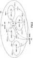
- FIG. 2 One example of a CoMP deployment scenario of interest is depicted in FIG. 2 .
- the UE 110 can transmit to the RRFHs 170-2, 170-3, and 170-4 and potentially the eNB 12.
- reception nodes 150 therefore include RRFHs 170-2, 170-3, and 170-4, and the eNB 12 receives baseband information 171 from the RRFHs 170-2, 170-3, and 170-4 and processes the baseband information 171 in the exemplary manners described below.
- the eNB 12 may have a receiver (e.g., as part of a transceiver 160) and a number of antennas 12E, and therefore the eNB 12 may form a reception node 150.
- FIG. 3 is a block diagram of a portion of a multipoint reception system with multiple reception nodes 150, in a general example to illustrate possible techniques for performing reception.
- the reception nodes are all RRFHs 170-1 through 170-N and are coupled to the baseband processor(s) 190.
- Each RRFH 170 in this example includes an analog to digital (A/D) converter 345, antenna(s) 158, a power amplifier 390, and a down converter 385.
- A/D analog to digital
- the RRFHs may have other configurations.
- the down converters 385 could come after the A/D converters 345 in the signal path (i.e., instead of before the A/D converters 345 as shown in FIG. 3 ).
- Each of the RRFHs 170 communicate digital time-domain signals 350 (i.e., 350-1 through 350-N) to the baseband processor(s) 190. It is noted that FIG. 3 only shows a portion of the receiver, Rx, of the transceiver 160 of the RRFH 170.
- Phase error is an inevitable problem for wireless communication systems in reality. Such phase error is manifested as carrier FO (Frequency Offset) and PN (Phase Noise) or phase jittering. It is well known that the impact of the carrier frequency offset and phase noise on OFDM (Orthogonal Frequency-Division Multiplexing) and SC-FDMA (Single Carrier - Frequency Division Multiple Access) signals is ICI (Inter-Carrier Interference) and received data symbol phase rotation. While there is not an easy way to remove ICI in practice, the received data symbol phase error can be simply corrected by phase de-rotation, once the associated FO is known, by FOE (Frequency Offset Estimation).
- FO Frequency Offset
- PN Phase Noise Noise
- a SC-FDMA technique has been used in 3GPP (third Generation Partnership Project) LTE (Long Term Evolution) uplink communication, which has a similar system throughput and essentially the same overall complexity as OFDMA (a variation of OFDM) while having a lower transmit PAPR (Peak to Average Power Ratio). Since two DFT (Digital Fourier Transform) and IDFT (Inverse Digital Fourier Transform) pairs are implemented in SC-FDMA transmitter and receiver, the impact of carrier FO and phase noise on LTE uplink is similar to that of OFDM. In other words, most LTE uplink receivers are left with phase jittering and ICI and only perform FOC associated with carrier FO.
- Downlink and uplink CoMP are advanced features of LTE, where multiple cells cooperatively serve a group of UE (User Equipment) and effectively form a "network MIMO" (Multiple-Input and Multiple-Output). From a synchronization perspective, some special questions have been raised for CoMP technology. These questions have been extensively investigated and well-understood for a traditional single cell transmitter and receiver.
- LTE uplink CoMP a number of non-co-located cells are expected to coordinately perform baseband signal processing for a particular UE. Due to physical distances among CoMP cells, or associated antennas, carrier FO seen by each cell will be different even for the same UE.
- the phase error resulting from carrier FO corresponds to continuous phase shift portion of ⁇ ( t ) over time that can be written as 2 ⁇ ft + ⁇ 0 , where ⁇ f is FO and ⁇ 0 is any initial phase.
- and E[ ⁇ ( t )] 0, where ⁇ denotes the one-sided 3 dB linewidth of the Lorentzian PDS (Power Density Spectrum) of the free-running carrier generator.
- the parameter c determines the noise floor; parameters a and f 1 represent characteristics of the PLL; b and f 2 indicate the steepness of a linear slope of the PDS and where the noise floor becomes dominant, respectively.
- c 10.5
- b 4
- a 6.5
- f 1 1000 Hz
- an MCLS Multi-Cell Link Simulator
- the MCLS has many functions of system level simulator, such as UE and cell drop, scheduler and power control, and the like.
- a list of cells for uplink CoMP is generated for each UE by using PL (Path Loss) of each drop.
- CDF Cumulative Distribution Function
- An FFT of a portion of N continuous time-domain samples associated with a p th SC-FDMA symbol provides a frequency-domain signal.
- the k th subcarrier of this SC-FDMA symbol can be expressed as the following: DFT y p
- carrier FO causes received SC-FDMA symbol common phase rotation, corresponding to e j ⁇ ( p ) , and a constant frequency shift represented by ⁇ f norm .
- ⁇ f norm a constant frequency shift represented by ⁇ f norm .
- an OFDM or SC-FDMA signal has a rectangular time-domain pulse shaping that translates to a frequency-domain sinc function.
- Samples of the sinc function are interference free if sampling instant is perfect. In other words, if the sampling instant is the center of each subcarrier, there is no interference or ICI.
- the frequency shift of X ( p ) k- ⁇ norm implies imperfect sampling instants of the sinc function and the imperfect sampling results in ICI. This FO induced ICI cannot be easily removed.
- Most practical LTE uplink receivers are left with this ICI and only correct phase error by de-rotation based on e j ⁇ ( p ) and e j ⁇ ( m ) to mitigate impact of carrier FO.
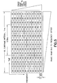
- An LTE uplink PRB (Physical Resource Block) pair is depicted in FIG. 5 , where each subframe has 2 PRBs, each of which includes 7 SC-FDMA symbols (0.5 ms) with a DMRS (De-modulation Reference Signal or RS for short) in the middle.
- DS in the figure stands for data symbol.
- Each PRB has 12 subcarriers in the frequency dimension. It is also shown that any timing offset and frequency offset cause phase ramp in frequency dimension and time dimension respectively. Therefore, FOE can be calculated based on the phase difference of the two RS, i.e. ⁇ (4)- ⁇ (11).
- ⁇ f is firstly calculated (see FOE 620 in FIG. 6 ) on frequency-domain signals 615 (see FIG. 6 ) from each antenna and a final FOE is obtained by averaging all such ⁇ f .
- the FFTs 610-1 through 610-N convert the digital time-domain signals 605 to frequency-domain signals 615.
- FOC is achieved by phase rotation based on e j ⁇ ( p ) and e j ⁇ ( m ) after antenna combining 640 (e.g., possibly including frequency-domain equalization) and IDFT 650, as shown in FIG. 6 , where CE, IRC and MRC are channel estimate, interference reduced combining and maximum ratio combining respectively.
- Exemplary CE techniques include but are not limited to the techniques presented in Ashraf Tahat, “Multi-User Channel Estimation in a 4G OFDM System", The 18th Annual IEEE International Symposium on Personal, Indoor and Mobile Radio Communications (PIMRC'07) (2007 ).
- Exemplary IRC techniques that may be used are presented in but are not limited to Y. Ohwatan et al., "Performance of Advanced Receiver Employing Interference Rejection Combining to Suppress Inter-cell Interference in LTE-Advanced Downlink", Vehicular Technology Conference (VTC Fall) (2011 ).
- FIG. 6 is a block diagram of an exemplary logic flow diagram that illustrates the operations for conventional frequency offset correction for collocated antennas.
- Each CE 630 creates a signal 635, which includes the signal 615 and additional CE information. Consequently, output 645 of the antenna combining 640 is converted back to the time-domain by the IDFT 650 (creating time-domain estimates in signal 655 of data symbols received from a UE) that is followed by phase de-rotation (FOC 660) on all data symbols based on the M x 12 matrix in the following: e ⁇ j ⁇ 1 + ⁇ ⁇ M / 2 e ⁇ j ⁇ 2 + ⁇ ⁇ M / 2 ⁇ e ⁇ j ⁇ 14 + ⁇ ⁇ M / 2 e ⁇ j ⁇ 1 + ⁇ ⁇ M / 2 + 1 e ⁇ j ⁇ 2 + ⁇ ⁇ M / 2 + 1 ⁇ e ⁇ j ⁇ 14 + ⁇ ⁇ M / 2 + 1 ⁇ ⁇ ⁇ M / 2 + 1 ⁇ e ⁇ j ⁇ 14 + ⁇ ⁇ M / 2 +
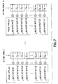
- FIG. 7 illustrates the application of the M ⁇ 12 graphically.
- the D in FIG. 7 corresponds to the DS in FIG. 5 .
- N CP p is written as a function of p to emphasize the number of CP for DMRS and data SC-FDMA symbols are different.
- This M ⁇ 12 matrix is multiplied with all data QAM (Quadrature Amplitude Modulation) symbols in a subframe element-by-element.
- the output 670 is a set of time-domain received symbols corresponding to a single UE. For each UE, the process from 620 to 670 should be performed again.
- FIG. 8 is a block diagram similar to the diagram in FIG. 6 , divided by cells (of which there are N in this example and a total of X antennas).
- the LTE DMRS is created based on well-known ZC (Zadoff-Chu) sequences with different frequency shifts.
- ZC Zero-Chu
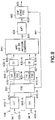
- FIG. 9 is a block diagram of an exemplary logic flow diagram implemented by a baseband processor 190 that illustrates the operations for frequency error correction for LTE uplink in a system with collocated antennas.
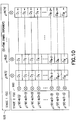
- FIG. 10 is a block diagram that illustrates mathematical operations for frequency offset correction in accordance with an exemplary embodiment of the instant invention.
- FOC e.g., FOC 660 as illustrated in FIG. 6 and graphically illustrated in FIG. 7
- FIGS. 9 and 10 point out that FOC (e.g., FOC 660 as illustrated in FIG. 6 and graphically illustrated in FIG. 7 ) is split into two stages, a first (1 st ) stage FOC 925 that is performed corresponding to each of the N antennas and a second (2 nd ) stage FOC 960 that is performed after IDFT 650.
- the output signal 927 of a first stage FOC 925 is a frequency-offset corrected signal.
- the signal 935 includes CE information and the signal 927.
- the output results 970 of FIG. 9 should be equivalent to the output results 670 of FIG. 6 .
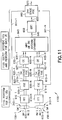
- FIG. 11 this figure is a block diagram 1100 of an exemplary logic flow diagram implemented by a baseband processor that illustrates the operations for frequency error correction for LTE uplink CoMP, where the operations may be considered to be an exemplary method, a result of execution of computer program instructions embodied on a computer readable memory, and/or functions performed by logic implemented in hardware, in accordance with exemplary embodiments of this invention.
- FOC for a CoMP system is achieved in two stages (see FIG.
- the first FOC stage 920-1 through 925-N is based on per cell e j ⁇ ( p ) that is calculated (by the corresponding FOE 920-1 through 920-N) using associated ⁇ f c and applied to all SC-FDMA symbols before corresponding CE 630-1 to 630-N and antenna combining 640;
- the second FOC stage 960 is based on e j ⁇ ( m ) that is calculated with averaged FOE over all cells in CoMP operation and applied to all data QAM symbols after antenna combining 640 and IDFT 650.
- Exemplary FOE techniques include the techniques presented in Hyunsoo Cheon, "Frequency Offset Estimation for High Speed Users in E-Utra Uplink", the 18th Annual IEEE International Symposium on Personal, Indoor and Mobile Radio Communications (PIMRC'07) (2007 ). Since the 2 nd stage FOC 960 uses the averaged FOE, this stage is suboptimum for the same issue of traditional post-IDFT FOC. However, due to the fact that the contribution of e j ⁇ ( m ) is significantly small compared with e j ⁇ ( p ) , this two-stage FOC structure delivers significant performance improvement for CoMP as shown in simulation results below. This also illustrates that the second stage FOC 960 is optional. For FIG. 10 as this is applied to the frequency correction of FIG.
- the Stage 1 FOC shown in FIG. 10 is one of the first stage FOCs 925-1 through 925-N. That is, each of the first stage FOC 925 performs calculations using phase e j ⁇ ( p ) for a ⁇ f c corresponding to a cell 310.
- the second stage FOC 960 receives all N ⁇ f c and determines the average ⁇ f shown in FIG. 10 and used in the second stage FOC 960.
- the blocks in FIG. 11 may be implemented by a baseband processor 190 as shown in FIG. 1 .
- each cell may include one or more antennas and the number of antennas per cell need not be the same (as shown in FIG. 2 ).
- the logic operations in FIG. 11 will typically, in practice, be performed by a single integrated circuit (such as an application-specific integrated circuit, e.g., a processor 150). However, it may be possible to perform these logic operations using multiple integrated circuits.
- the FFTs 610-1 through 610-N are performed for all UEs at the same time (as illustrated by reference 1110), whereas the FOEs 920-1 through 920-N, and the first stage FOCs 925-1 through 925-N, the CE 630-1 through 630-N, antenna combining 640, IDFT 650, and second stage FOC 960 are performed for each UE (as illustrated by reference 1120) separately.
- the antenna combining 640 treats other UEs as interferers and reduces their impact on the desired UE.
- FIG. 10 shows 2-stage FOC for a desired UE, where one can consider the other UEs using the PRB structure as interferers whose impact will be reduced by antenna combining in the frequency domain.
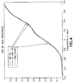
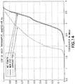
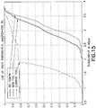
- the reference (“No FO&PN”) is an ideal scenario that does not have either phase noise or FO.
- the "Current FOC” was calculated using the techniques described above in reference to FIGS. 7 and 8 .
- the "New FOC” was calculated using the techniques described above in reference to FIGS. 10 and 11 . In FIG.
- each of the three curves is basically indistinguishable.
- the CDF means that about 30 percent of users get 3 Mbps or less of throughput.
- a gap develops between the curve for the Current FOC and the curve for the New FOC, although the differences are small between the curves for the New FOC and the No FO&PN.
- FIG. 15 150 Hz
- the gap is large between the curve for the Current FOC and the curve for the New FOC, although the differences become more significant between the curves for the New FOC and the No FO&PN.
- the gap between the New FOC and the No FO&PN in FIG. 15 is due to ICI and suboptimal second stage FOC.
- Antenna combining across cells has the potential issue of the receiver having to handle different frequency offsets on different cells.
- Current receivers show significant performance loss due to joint estimation and correction approach across all antennas.
- a new FOC technique proposed herein shows significant improvement.
- the exemplary embodiments of the invention can be applied to any IRC receiver with multiple antennas having different FO, such as CRAN, DRAN and small cell systems.
- Embodiments of the present invention may be implemented in software (executed by one or more processors), hardware (e.g., an application specific integrated circuit), or a combination of software and hardware.
- the software e.g., application logic, an instruction set
- a "computer-readable medium” may be any media or means that can contain, store, communicate, propagate or transport the instructions for use by or in connection with an instruction execution system, apparatus, or device, such as a computer, with one example of a computer described and depicted, e.g., in FIG. 1 .
- a computer-readable medium may comprise a computer-readable storage medium (e.g., memory(ies) 155 195 or other device) that may be any media or means that can contain or store the instructions for use by or in connection with an instruction execution system, apparatus, or device, such as a computer.
- a computer-readable storage medium e.g., memory(ies) 155 195 or other device
- the different functions discussed herein may be performed in a different order and/or concurrently with each other. Furthermore, if desired, one or more of the above-described functions may be optional or may be combined.
Landscapes
- Engineering & Computer Science (AREA)
- Signal Processing (AREA)
- Computer Networks & Wireless Communication (AREA)
- Power Engineering (AREA)
- Radio Transmission System (AREA)
- Mobile Radio Communication Systems (AREA)
Claims (13)
- Verfahren (1100), umfassend:für ein ausgewähltes Benutzergerät (110) für Signale (615), die mindestens teilweise dem ausgewählten Benutzergerät (110) entsprechen und durch Antennen (158) von mehreren Zellen (310) empfangen wurden, wobei jede Zelle (310) eine oder mehrere Antennen (158) aufweist und wobei jedes Signal (615) von einer einzelnen der Antennen (158) stammt, Durchführen (1120) des Folgenden:Schätzen eines Trägerfrequenzoffsets (920) für jede Zelle (310) unter Verwendung von einem oder mehreren der Signale (615) von der Zelle (310);Durchführen von Frequenzoffsetkorrektur (925) an jedem Signal (615) von jeder Zelle (310) unter Verwendung mindestens des geschätzten Trägerfrequenzoffsets für eine assoziierte Zelle (310);Schätzen eines Kanals (630) für jedes frequenzoffsetkorrigierte Signal (935);Kombinieren (640), unter Verwendung des geschätzten Kanals, von jedem der frequenzoffsetkorrigierten Signale (935), um eine odermehrere Schätzungen (645) von einem oder mehreren von dem ausgewählten Benutzergerät (110) gesendeten Symbolen zu erzeugen,Durchführen einer inversen diskreten Fourier-Transformation (650), um Zeitbereichsversionen (655) der einen oder der mehreren Schätzungen (645) von dem einen oder den mehreren von dem ausgewählten Benutzergerät (110) gesendeten Symbolen zu erzeugen, undDurchführen einer zweiten Frequenzoffsetkorrektur (960) an den Zeitbereichsversionen (655) der einen oder der mehreren Schätzungen (645) durch Multiplizieren ausgewählter Symbole (960) eines physischen Ressourcenblocks in einem Unterrahmen eines entsprechenden Frequenzdomänensignals (615) durch einen zweiten Phasenfaktor, der einem Mittelwert der geschätzten Trägerfrequenzoffsets entspricht, wobei die zweite Frequenzoffsetkorrektur ferner Zeitbereichsversionen (970) der einen oder der mehreren Schätzungen von dem einen oder den mehreren von dem ausgewählten Benutzergerät (110) gesendeten Symbolen erzeugt.
- Verfahren (1100) nach Anspruch 1, wobei jeder Trägerfrequenzoffset einer Differenz zwischen einem durch einen Empfänger (Rx, 160) in einer einzelnen der Zellen (310) empfangenen Träger und einem durch einen Sender (Tx, 130) in dem Benutzergerät (110) gesendeten Träger entspricht.
- Verfahren (1100) nach einem der Ansprüche 1 bis 2, wobei jedes Signal ein Frequenzdomänensignal (615) ist und wobei Durchführen von Frequenzoffsetkorrektur ferner Multiplizieren (925), für jedes der Frequenzdomänensignale (615), von ausgewählten Symbolen eines physischen Ressourcenblocks in einem Unterrahmen eines entsprechenden Frequenzdomänensignals (615) durch einen Phasenfaktor, der einem geschätzten Trägerfrequenzoffset für eine dem Frequenzdomänensignal (615) entsprechende Zelle (310) entspricht, umfasst.
- Verfahren (1100) nach Anspruch 3, wobei Multiplizieren (925) ferner Multiplizieren der ausgewählten Symbole des physischen Ressourcenblocks in dem Frequenzdomänensignal (615) durch den Phasenfaktor e -jΦ(p) umfasst, wobei Φ(p) = 2πΔfcTs [(p-1)N+

- Verfahren (1100) nach Anspruch 4, ferner umfassend Durchführen, für jedes Frequenzdomänensignal (615), einer diskreten Fourier-Transformation (610), um ein Zeitdomänensignal (605) für eine entsprechende Antenne (158) in das Frequenzdomänensignal (615) umzuwandeln, wobei jede diskrete Fourier-Transformation (610) die Größe N aufweist.
- Verfahren (1100) nach Anspruch 1, wobei Multiplizieren (960) der ausgewählten Symbole des physischen Ressourcenblocks in dem Unterrahmen durch den zweiten Phasenfaktor ferner Multiplizieren (960) der ausgewählten Symbole des physischen Ressourcenblocks in dem Unterrahmen durch den zweiten Phasenfaktor e -jΨ(m) umfasst, wobei Ψ(m) = 2πΔfnormm/M ist, wobei Δf norm der Mittelwert der geschätzten Trägerfrequenzoffsets ist, m ein Zeitindex ist und m=-M/2,-M/2+1,...,0,1,...M/2-1 ist.
- Verfahren (1100) nach einem der vorhergehenden Ansprüche, ferner umfassend Auswählen (1120) eines anderen Benutzergeräts (110) und Durchführen mindestens des Schätzens von Trägerfrequenzoffset (920), des Durchführens von Frequenzoffsetkorrektur (925), des Schätzens eines Kanals (630) und des Kombinierens (640) für das andere Benutzergerät (110), wobei diskrete Fourier-Transformationen (610) zum Umwandeln von digitalen Zeitdomänensignalen (605) für Antennen (158) in Frequenzdomänensignale (615) für alle Benutzergeräte (110) durchgeführt werden (1110).
- Computerprogrammprodukt, das Programmcode zum Ausführen des Verfahrens (1100) nach einem der Ansprüche 1 bis 7 umfasst.
- Computerprogramm nach Anspruch 8, wobei das Computerprogramm ein Computerprogrammprodukt ist, das ein computerlesbares Medium (195) umfasst, das einen darin zur Verwendung mit einem Computer (190) umgesetzten Computerprogrammcode (197) führt.
- Vorrichtung (190, 1100), umfassend:für ein ausgewähltes Benutzergerät (110) für Signale, die mindestens teilweise dem ausgewählten Benutzergerät (110) entsprechen und durch Antennen (158) von mehreren Zellen empfangen wurden, wobei jede Zelle (310) eine oder mehrere Antennen (158) aufweist und wobei jedes Signal von einer einzelnen der Antennen (158) stammt, Mittel umfassend:ein Mittel zum Schätzen eines Trägerfrequenzoffsets (920) für jede Zelle (310) unter Verwendung von einem oder mehreren der Signale von der Zelle (310);ein Mittel zum Durchführen von Frequenzoffsetkorrektur (925) an jedem Signal (615) von jeder Zelle (310) unter Verwendung mindestens des geschätzten Trägerfrequenzoffsets für eine assoziierte Zelle (310);ein Mittel zum Schätzen eines Kanals (630) für jedes frequenzoffsetkorrigierte Signal (927);ein Mittel zum Kombinieren (640), unter Verwendung des geschätzten Kanals, von jedem der frequenzoffsetkorrigierten Signale (927), um eine oder mehrere Schätzungen (645) von einem oder mehreren von dem ausgewählten Benutzergerät (110) gesendeten Symbolen zu erzeugen,ein Mittel zum Durchführen einer inversen diskreten Fourier-Transformation (650), um Zeitbereichsversionen (655) der einen oder der mehreren Schätzungen (645) von dem einen oder den mehreren von dem ausgewählten Benutzergerät (110) gesendeten Symbolen zu erzeugen, undein Mittel zum Durchführen einer zweiten Frequenzoffsetkorrektur (960) an den Zeitbereichsversionen (655) der einen oder der mehreren Schätzungen (645) durch Multiplizieren ausgewählter Symbole (960) eines physischen Ressourcenblocks in einem Unterrahmen eines entsprechenden Frequenzdomänensignals (615) durch einen zweiten Phasenfaktor, der einem Mittelwert der geschätzten Trägerfrequenzoffsets entspricht, wobei die zweite Frequenzoffsetkorrektur ferner Zeitbereichsversionen (970) der einen oder der mehreren Schätzungen von dem einen oder den mehreren von dem ausgewählten Benutzergerät (110) gesendeten Symbolen erzeugt.
- Vorrichtung (190, 1100) nach Anspruch 10, wobei jeder Trägerfrequenzoffset einer Differenz zwischen einem durch einen Empfänger (Rx, 160) in einer einzelnen der Zellen (310) empfangenen Träger und einem durch einen Sender (Tx, 130) in dem Benutzergerät (110) gesendeten Träger entspricht.
- Vorrichtung (190, 1100) nach einem der Ansprüche 10 bis 11, wobei jedes Signal ein Frequenzdomänensignal (615) ist und wobei das Mittel zum Durchführen von Frequenzoffsetkorrektur ferner ein Mittel zum Multiplizieren (925), für jedes der Frequenzdomänensignale (615), von ausgewählten Symbolen eines physischen Ressourcenblocks in einem Unterrahmen eines entsprechenden Frequenzdomänensignals (615) durch einen Phasenfaktor, der einem geschätzten Trägerfrequenzoffset für eine dem Frequenzdomänensignal (615) entsprechende Zelle (310) entspricht, umfasst.
- Vorrichtung nach Anspruch 10, umfassend ein Mittel zum Durchführen eines Verfahrens nach einem der Ansprüche 4 bis 7.
Priority Applications (1)
| Application Number | Priority Date | Filing Date | Title |
|---|---|---|---|
| PL12772846T PL2920933T3 (pl) | 2012-09-24 | 2012-09-24 | Korekcja błędu częstotliwości dla lte uplink comp |
Applications Claiming Priority (1)
| Application Number | Priority Date | Filing Date | Title |
|---|---|---|---|
| PCT/US2012/056842 WO2014046684A1 (en) | 2012-09-24 | 2012-09-24 | Frequency error correction for lte uplink comp |
Publications (2)
| Publication Number | Publication Date |
|---|---|
| EP2920933A1 EP2920933A1 (de) | 2015-09-23 |
| EP2920933B1 true EP2920933B1 (de) | 2018-04-18 |
Family
ID=47019153
Family Applications (1)
| Application Number | Title | Priority Date | Filing Date |
|---|---|---|---|
| EP12772846.7A Not-in-force EP2920933B1 (de) | 2012-09-24 | 2012-09-24 | Frequenzfehlerkorrektur für lte uplink comp |
Country Status (5)
| Country | Link |
|---|---|
| US (1) | US9629158B2 (de) |
| EP (1) | EP2920933B1 (de) |
| CN (1) | CN104982015B (de) |
| PL (1) | PL2920933T3 (de) |
| WO (1) | WO2014046684A1 (de) |
Families Citing this family (17)
| Publication number | Priority date | Publication date | Assignee | Title |
|---|---|---|---|---|
| CN105337911B (zh) * | 2014-08-07 | 2019-12-03 | 中兴通讯股份有限公司 | 一种子载波间干扰的消除方法和装置 |
| US10454739B2 (en) * | 2015-01-23 | 2019-10-22 | Texas Instruments Incorporated | Transmission scheme for SC-FDMA with two DFT-precoding stages |
| WO2017162903A1 (en) | 2016-03-23 | 2017-09-28 | Nokia Technologies Oy | Common phase error and/or inter-carrier interference |
| EP3451601B1 (de) | 2016-04-25 | 2021-10-06 | LG Electronics Inc. | Signalübertragungsverfahren zur schätzung von phasenrauschen in einem drahtloskommunikationssystem |
| CN107370698B (zh) * | 2016-05-13 | 2021-11-30 | 中兴通讯股份有限公司 | 一种下行信号处理方法、装置及基站 |
| CN106452674B (zh) * | 2016-09-30 | 2019-04-12 | 西安交通大学 | 一种基于802.11ac网络的实际数据包恢复方法 |
| TWI630800B (zh) * | 2016-10-21 | 2018-07-21 | 財團法人工業技術研究院 | 協調式多點傳輸方法和基地台 |
| CN108174439B (zh) * | 2016-12-07 | 2021-02-26 | 财团法人工业技术研究院 | 多基站系统及其信道校正方法 |
| WO2018143537A1 (ko) * | 2017-02-03 | 2018-08-09 | 엘지전자(주) | 무선 통신 시스템에서 위상 잡음을 추정하기 위한 방법 및 이를 위한 장치 |
| US10382244B2 (en) * | 2017-02-14 | 2019-08-13 | Samsung Electronics Co., Ltd. | System and method for providing time offset and frequency offset estimation for vehicle to everything communication system |
| DE112017007385T5 (de) * | 2017-04-01 | 2019-12-12 | Intel IP Corporation | Synchronisieren einer digitalen frequenzverschiebung |
| KR102265906B1 (ko) | 2017-10-12 | 2021-06-16 | 엘지전자 주식회사 | 무선 통신 시스템에서 단말의 위상 트래킹 참조 신호 수신 방법 및 이를 지원하는 장치 |
| CN109729032B (zh) * | 2017-10-31 | 2021-09-24 | 深圳市中兴微电子技术有限公司 | 一种频偏估计值的校正方法、装置及计算机可读存储介质 |
| US10355842B2 (en) | 2017-12-07 | 2019-07-16 | Lg Electronics Inc. | Method of transmitting uplink phase tracking reference signal by user equipment in wireless communication system and apparatus supporting same |
| WO2019232801A1 (en) * | 2018-06-08 | 2019-12-12 | Nokia Shanghai Bell Co., Ltd. | Noise floor estimation for signal detection |
| TWI717736B (zh) | 2019-05-15 | 2021-02-01 | 財團法人工業技術研究院 | 多天線系統及其通道校正方法 |
| US11115860B1 (en) | 2020-03-19 | 2021-09-07 | Sprint Communications Company L.P. | Secondary access node control in a wireless communication network |
Family Cites Families (10)
| Publication number | Priority date | Publication date | Assignee | Title |
|---|---|---|---|---|
| US6275543B1 (en) * | 1996-10-11 | 2001-08-14 | Arraycomm, Inc. | Method for reference signal generation in the presence of frequency offsets in a communications station with spatial processing |
| US5878093A (en) | 1996-12-16 | 1999-03-02 | Ericsson Inc. | Interference rejection combining with frequency correction |
| WO2002098094A1 (en) * | 2001-05-31 | 2002-12-05 | Nortel Networks Limited | Apparatus and method for measuring sub-carrier frequencies and sub-carrier frequency offsets |
| US7173990B2 (en) | 2001-12-27 | 2007-02-06 | Dsp Group Inc. | Joint equalization, soft-demapping and phase error correction in wireless system with receive diversity |
| CN101136881B (zh) * | 2006-08-31 | 2012-10-10 | 世意法(北京)半导体研发有限责任公司 | 一种ofdma上行链路接收机和估计载波频偏的方法 |
| CA2667026C (en) * | 2006-10-05 | 2015-12-01 | Cohda Wireless Pty Ltd | Improving receiver performance in a communication network |
| CN101938444B (zh) * | 2009-06-30 | 2014-06-18 | 中兴通讯股份有限公司 | 正交频分复用系统的频偏估计与校正的方法及装置 |
| US8576692B2 (en) * | 2009-09-10 | 2013-11-05 | Qualcomm Incorporated | Transmission of UE-specific reference signal for wireless communication |
| WO2012027793A1 (en) * | 2010-09-01 | 2012-03-08 | Commonwealth Scientific And Industrial Research Organisation | Channel estimation in a multi-user mimo-ofdm system in the presence of user terminal symbol-specific phase offsets |
| CN102546113B (zh) * | 2012-01-19 | 2014-11-26 | 新邮通信设备有限公司 | 一种lte的信道测量及反馈方法 |
-
2012
- 2012-09-24 EP EP12772846.7A patent/EP2920933B1/de not_active Not-in-force
- 2012-09-24 CN CN201280077246.8A patent/CN104982015B/zh not_active Expired - Fee Related
- 2012-09-24 US US14/430,699 patent/US9629158B2/en not_active Expired - Fee Related
- 2012-09-24 PL PL12772846T patent/PL2920933T3/pl unknown
- 2012-09-24 WO PCT/US2012/056842 patent/WO2014046684A1/en not_active Ceased
Non-Patent Citations (1)
| Title |
|---|
| None * |
Also Published As
| Publication number | Publication date |
|---|---|
| PL2920933T3 (pl) | 2018-09-28 |
| WO2014046684A1 (en) | 2014-03-27 |
| EP2920933A1 (de) | 2015-09-23 |
| US20150282171A1 (en) | 2015-10-01 |
| CN104982015B (zh) | 2018-11-16 |
| CN104982015A (zh) | 2015-10-14 |
| US9629158B2 (en) | 2017-04-18 |
Similar Documents
| Publication | Publication Date | Title |
|---|---|---|
| US9629158B2 (en) | Frequency error correction for LTE uplink CoMP | |
| Lim et al. | SIR analysis of OFDM and GFDM waveforms with timing offset, CFO, and phase noise | |
| US10063401B2 (en) | Communication method and apparatus based on a filter bank multi-carrier modulation | |
| US20230318894A1 (en) | Pilot transmission method and apparatus, network side device, and storage medium | |
| US20170331663A1 (en) | Systems, devices and methods for communicating data over circularly pulse-shaped waveforms | |
| EP3127292B1 (de) | Hybrides wellenformdesign mit kombination von ofdm und auf zyklischem präfix basierendem träger zur drahtlosen millimeterwellenkommunikation | |
| EP2628254B1 (de) | Uplink-rauschschätzung für virtuelles mimo | |
| US10148463B2 (en) | Method and device for estimating frequency offset | |
| Kotzsch et al. | Interference analysis in time and frequency asynchronous network MIMO OFDM systems | |
| CN103379078A (zh) | 一种频域均衡检测的方法和设备 | |
| Choi et al. | Effect of timing and frequency synchronization errors on GFDM systems | |
| Wan et al. | Robust multi-user channel tracking scheme for 5G new radio | |
| US20130279632A1 (en) | Method of modulating signal for data communication and device therof | |
| Lee et al. | Time and frequency synchronization for OFDMA uplink system using the SAGE algorithm | |
| EP2806611A1 (de) | Offset-Schätzung mittels Kanalzustandsinformationsreferenzsymbolen und Demodulationsreferenzsymbolen | |
| Sibel | Tracking the phase noise in sub-THz bands | |
| Zhang et al. | Multi-service signal multiplexing and isolation for physical-layer network slicing (PNS) | |
| Ranjha et al. | Interference analysis of interleaved and localized mapping schemes in OFDMA system with Carrier Frequency Offset | |
| Lim et al. | Optimal receiver filter for GFDM with timing and frequency offsets in uplink multiuser systems | |
| Yang et al. | Windowed OFDM for mixed‐numerology 5G and beyond systems | |
| Kalwar et al. | Analysis of effect of carrier frequency offset on performance of LTE uplink | |
| Sabeti et al. | CFO estimation for OFDM-based massive MIMO systems in asymptotic regime | |
| Ba et al. | Performance evaluation of lte and 5g modeling over OFDM and GFDM physical layers | |
| Zhu et al. | CFO estimation and compensation in single carrier interleaved FDMA systems | |
| Ghogho et al. | Frame and frequency acquisition for OFDM |
Legal Events
| Date | Code | Title | Description |
|---|---|---|---|
| PUAI | Public reference made under article 153(3) epc to a published international application that has entered the european phase |
Free format text: ORIGINAL CODE: 0009012 |
|
| 17P | Request for examination filed |
Effective date: 20150424 |
|
| AK | Designated contracting states |
Kind code of ref document: A1 Designated state(s): AL AT BE BG CH CY CZ DE DK EE ES FI FR GB GR HR HU IE IS IT LI LT LU LV MC MK MT NL NO PL PT RO RS SE SI SK SM TR |
|
| AX | Request for extension of the european patent |
Extension state: BA ME |
|
| DAX | Request for extension of the european patent (deleted) | ||
| 17Q | First examination report despatched |
Effective date: 20160518 |
|
| GRAP | Despatch of communication of intention to grant a patent |
Free format text: ORIGINAL CODE: EPIDOSNIGR1 |
|
| INTG | Intention to grant announced |
Effective date: 20171106 |
|
| GRAS | Grant fee paid |
Free format text: ORIGINAL CODE: EPIDOSNIGR3 |
|
| GRAA | (expected) grant |
Free format text: ORIGINAL CODE: 0009210 |
|
| STAA | Information on the status of an ep patent application or granted ep patent |
Free format text: STATUS: THE PATENT HAS BEEN GRANTED |
|
| AK | Designated contracting states |
Kind code of ref document: B1 Designated state(s): AL AT BE BG CH CY CZ DE DK EE ES FI FR GB GR HR HU IE IS IT LI LT LU LV MC MK MT NL NO PL PT RO RS SE SI SK SM TR |
|
| REG | Reference to a national code |
Ref country code: GB Ref legal event code: FG4D |
|
| REG | Reference to a national code |
Ref country code: CH Ref legal event code: EP |
|
| REG | Reference to a national code |
Ref country code: AT Ref legal event code: REF Ref document number: 991592 Country of ref document: AT Kind code of ref document: T Effective date: 20180515 |
|
| REG | Reference to a national code |
Ref country code: IE Ref legal event code: FG4D |
|
| REG | Reference to a national code |
Ref country code: DE Ref legal event code: R096 Ref document number: 602012045359 Country of ref document: DE |
|
| REG | Reference to a national code |
Ref country code: NL Ref legal event code: FP |
|
| REG | Reference to a national code |
Ref country code: LT Ref legal event code: MG4D |
|
| PG25 | Lapsed in a contracting state [announced via postgrant information from national office to epo] |
Ref country code: LT Free format text: LAPSE BECAUSE OF FAILURE TO SUBMIT A TRANSLATION OF THE DESCRIPTION OR TO PAY THE FEE WITHIN THE PRESCRIBED TIME-LIMIT Effective date: 20180418 Ref country code: BG Free format text: LAPSE BECAUSE OF FAILURE TO SUBMIT A TRANSLATION OF THE DESCRIPTION OR TO PAY THE FEE WITHIN THE PRESCRIBED TIME-LIMIT Effective date: 20180718 Ref country code: ES Free format text: LAPSE BECAUSE OF FAILURE TO SUBMIT A TRANSLATION OF THE DESCRIPTION OR TO PAY THE FEE WITHIN THE PRESCRIBED TIME-LIMIT Effective date: 20180418 Ref country code: SE Free format text: LAPSE BECAUSE OF FAILURE TO SUBMIT A TRANSLATION OF THE DESCRIPTION OR TO PAY THE FEE WITHIN THE PRESCRIBED TIME-LIMIT Effective date: 20180418 Ref country code: FI Free format text: LAPSE BECAUSE OF FAILURE TO SUBMIT A TRANSLATION OF THE DESCRIPTION OR TO PAY THE FEE WITHIN THE PRESCRIBED TIME-LIMIT Effective date: 20180418 Ref country code: NO Free format text: LAPSE BECAUSE OF FAILURE TO SUBMIT A TRANSLATION OF THE DESCRIPTION OR TO PAY THE FEE WITHIN THE PRESCRIBED TIME-LIMIT Effective date: 20180718 Ref country code: AL Free format text: LAPSE BECAUSE OF FAILURE TO SUBMIT A TRANSLATION OF THE DESCRIPTION OR TO PAY THE FEE WITHIN THE PRESCRIBED TIME-LIMIT Effective date: 20180418 |
|
| PG25 | Lapsed in a contracting state [announced via postgrant information from national office to epo] |
Ref country code: RS Free format text: LAPSE BECAUSE OF FAILURE TO SUBMIT A TRANSLATION OF THE DESCRIPTION OR TO PAY THE FEE WITHIN THE PRESCRIBED TIME-LIMIT Effective date: 20180418 Ref country code: LV Free format text: LAPSE BECAUSE OF FAILURE TO SUBMIT A TRANSLATION OF THE DESCRIPTION OR TO PAY THE FEE WITHIN THE PRESCRIBED TIME-LIMIT Effective date: 20180418 Ref country code: GR Free format text: LAPSE BECAUSE OF FAILURE TO SUBMIT A TRANSLATION OF THE DESCRIPTION OR TO PAY THE FEE WITHIN THE PRESCRIBED TIME-LIMIT Effective date: 20180719 Ref country code: HR Free format text: LAPSE BECAUSE OF FAILURE TO SUBMIT A TRANSLATION OF THE DESCRIPTION OR TO PAY THE FEE WITHIN THE PRESCRIBED TIME-LIMIT Effective date: 20180418 |
|
| PGFP | Annual fee paid to national office [announced via postgrant information from national office to epo] |
Ref country code: SK Payment date: 20180730 Year of fee payment: 14 |
|
| REG | Reference to a national code |
Ref country code: AT Ref legal event code: MK05 Ref document number: 991592 Country of ref document: AT Kind code of ref document: T Effective date: 20180418 |
|
| PG25 | Lapsed in a contracting state [announced via postgrant information from national office to epo] |
Ref country code: PT Free format text: LAPSE BECAUSE OF FAILURE TO SUBMIT A TRANSLATION OF THE DESCRIPTION OR TO PAY THE FEE WITHIN THE PRESCRIBED TIME-LIMIT Effective date: 20180820 |
|
| REG | Reference to a national code |
Ref country code: DE Ref legal event code: R097 Ref document number: 602012045359 Country of ref document: DE |
|
| PG25 | Lapsed in a contracting state [announced via postgrant information from national office to epo] |
Ref country code: DK Free format text: LAPSE BECAUSE OF FAILURE TO SUBMIT A TRANSLATION OF THE DESCRIPTION OR TO PAY THE FEE WITHIN THE PRESCRIBED TIME-LIMIT Effective date: 20180418 Ref country code: RO Free format text: LAPSE BECAUSE OF FAILURE TO SUBMIT A TRANSLATION OF THE DESCRIPTION OR TO PAY THE FEE WITHIN THE PRESCRIBED TIME-LIMIT Effective date: 20180418 Ref country code: SK Free format text: LAPSE BECAUSE OF FAILURE TO SUBMIT A TRANSLATION OF THE DESCRIPTION OR TO PAY THE FEE WITHIN THE PRESCRIBED TIME-LIMIT Effective date: 20180418 Ref country code: CZ Free format text: LAPSE BECAUSE OF FAILURE TO SUBMIT A TRANSLATION OF THE DESCRIPTION OR TO PAY THE FEE WITHIN THE PRESCRIBED TIME-LIMIT Effective date: 20180418 Ref country code: EE Free format text: LAPSE BECAUSE OF FAILURE TO SUBMIT A TRANSLATION OF THE DESCRIPTION OR TO PAY THE FEE WITHIN THE PRESCRIBED TIME-LIMIT Effective date: 20180418 Ref country code: AT Free format text: LAPSE BECAUSE OF FAILURE TO SUBMIT A TRANSLATION OF THE DESCRIPTION OR TO PAY THE FEE WITHIN THE PRESCRIBED TIME-LIMIT Effective date: 20180418 |
|
| PLBE | No opposition filed within time limit |
Free format text: ORIGINAL CODE: 0009261 |
|
| STAA | Information on the status of an ep patent application or granted ep patent |
Free format text: STATUS: NO OPPOSITION FILED WITHIN TIME LIMIT |
|
| PG25 | Lapsed in a contracting state [announced via postgrant information from national office to epo] |
Ref country code: IT Free format text: LAPSE BECAUSE OF FAILURE TO SUBMIT A TRANSLATION OF THE DESCRIPTION OR TO PAY THE FEE WITHIN THE PRESCRIBED TIME-LIMIT Effective date: 20180418 Ref country code: SM Free format text: LAPSE BECAUSE OF FAILURE TO SUBMIT A TRANSLATION OF THE DESCRIPTION OR TO PAY THE FEE WITHIN THE PRESCRIBED TIME-LIMIT Effective date: 20180418 |
|
| 26N | No opposition filed |
Effective date: 20190121 |
|
| PG25 | Lapsed in a contracting state [announced via postgrant information from national office to epo] |
Ref country code: MC Free format text: LAPSE BECAUSE OF FAILURE TO SUBMIT A TRANSLATION OF THE DESCRIPTION OR TO PAY THE FEE WITHIN THE PRESCRIBED TIME-LIMIT Effective date: 20180418 |
|
| REG | Reference to a national code |
Ref country code: CH Ref legal event code: PL |
|
| PG25 | Lapsed in a contracting state [announced via postgrant information from national office to epo] |
Ref country code: SI Free format text: LAPSE BECAUSE OF FAILURE TO SUBMIT A TRANSLATION OF THE DESCRIPTION OR TO PAY THE FEE WITHIN THE PRESCRIBED TIME-LIMIT Effective date: 20180418 |
|
| REG | Reference to a national code |
Ref country code: BE Ref legal event code: MM Effective date: 20180930 |
|
| REG | Reference to a national code |
Ref country code: IE Ref legal event code: MM4A |
|
| PG25 | Lapsed in a contracting state [announced via postgrant information from national office to epo] |
Ref country code: LU Free format text: LAPSE BECAUSE OF NON-PAYMENT OF DUE FEES Effective date: 20180924 |
|
| PG25 | Lapsed in a contracting state [announced via postgrant information from national office to epo] |
Ref country code: IE Free format text: LAPSE BECAUSE OF NON-PAYMENT OF DUE FEES Effective date: 20180924 |
|
| PG25 | Lapsed in a contracting state [announced via postgrant information from national office to epo] |
Ref country code: BE Free format text: LAPSE BECAUSE OF NON-PAYMENT OF DUE FEES Effective date: 20180930 Ref country code: FR Free format text: LAPSE BECAUSE OF NON-PAYMENT OF DUE FEES Effective date: 20180930 Ref country code: CH Free format text: LAPSE BECAUSE OF NON-PAYMENT OF DUE FEES Effective date: 20180930 Ref country code: LI Free format text: LAPSE BECAUSE OF NON-PAYMENT OF DUE FEES Effective date: 20180930 |
|
| PGFP | Annual fee paid to national office [announced via postgrant information from national office to epo] |
Ref country code: DE Payment date: 20190910 Year of fee payment: 8 Ref country code: NL Payment date: 20190912 Year of fee payment: 8 |
|
| PGFP | Annual fee paid to national office [announced via postgrant information from national office to epo] |
Ref country code: GB Payment date: 20190919 Year of fee payment: 8 |
|
| PG25 | Lapsed in a contracting state [announced via postgrant information from national office to epo] |
Ref country code: MT Free format text: LAPSE BECAUSE OF NON-PAYMENT OF DUE FEES Effective date: 20180924 |
|
| PG25 | Lapsed in a contracting state [announced via postgrant information from national office to epo] |
Ref country code: TR Free format text: LAPSE BECAUSE OF FAILURE TO SUBMIT A TRANSLATION OF THE DESCRIPTION OR TO PAY THE FEE WITHIN THE PRESCRIBED TIME-LIMIT Effective date: 20180418 |
|
| PG25 | Lapsed in a contracting state [announced via postgrant information from national office to epo] |
Ref country code: HU Free format text: LAPSE BECAUSE OF FAILURE TO SUBMIT A TRANSLATION OF THE DESCRIPTION OR TO PAY THE FEE WITHIN THE PRESCRIBED TIME-LIMIT; INVALID AB INITIO Effective date: 20120924 Ref country code: MK Free format text: LAPSE BECAUSE OF NON-PAYMENT OF DUE FEES Effective date: 20180418 Ref country code: CY Free format text: LAPSE BECAUSE OF FAILURE TO SUBMIT A TRANSLATION OF THE DESCRIPTION OR TO PAY THE FEE WITHIN THE PRESCRIBED TIME-LIMIT Effective date: 20180418 |
|
| PG25 | Lapsed in a contracting state [announced via postgrant information from national office to epo] |
Ref country code: IS Free format text: LAPSE BECAUSE OF FAILURE TO SUBMIT A TRANSLATION OF THE DESCRIPTION OR TO PAY THE FEE WITHIN THE PRESCRIBED TIME-LIMIT Effective date: 20180818 |
|
| REG | Reference to a national code |
Ref country code: DE Ref legal event code: R119 Ref document number: 602012045359 Country of ref document: DE |
|
| REG | Reference to a national code |
Ref country code: NL Ref legal event code: MM Effective date: 20201001 |
|
| GBPC | Gb: european patent ceased through non-payment of renewal fee |
Effective date: 20200924 |
|
| PG25 | Lapsed in a contracting state [announced via postgrant information from national office to epo] |
Ref country code: NL Free format text: LAPSE BECAUSE OF NON-PAYMENT OF DUE FEES Effective date: 20201001 |
|
| PG25 | Lapsed in a contracting state [announced via postgrant information from national office to epo] |
Ref country code: DE Free format text: LAPSE BECAUSE OF NON-PAYMENT OF DUE FEES Effective date: 20210401 |
|
| PG25 | Lapsed in a contracting state [announced via postgrant information from national office to epo] |
Ref country code: GB Free format text: LAPSE BECAUSE OF NON-PAYMENT OF DUE FEES Effective date: 20200924 |
|
| PG25 | Lapsed in a contracting state [announced via postgrant information from national office to epo] |
Ref country code: PL Free format text: LAPSE BECAUSE OF NON-PAYMENT OF DUE FEES Effective date: 20190924 |