EP2919319A1 - Transmission line interconnect - Google Patents
Transmission line interconnect Download PDFInfo
- Publication number
- EP2919319A1 EP2919319A1 EP15158300.2A EP15158300A EP2919319A1 EP 2919319 A1 EP2919319 A1 EP 2919319A1 EP 15158300 A EP15158300 A EP 15158300A EP 2919319 A1 EP2919319 A1 EP 2919319A1
- Authority
- EP
- European Patent Office
- Prior art keywords
- transmission line
- interconnect
- coupling surface
- antenna
- molding compound
- Prior art date
- Legal status (The legal status is an assumption and is not a legal conclusion. Google has not performed a legal analysis and makes no representation as to the accuracy of the status listed.)
- Granted
Links
Images







Classifications
-
- H—ELECTRICITY
- H01—ELECTRIC ELEMENTS
- H01P—WAVEGUIDES; RESONATORS, LINES, OR OTHER DEVICES OF THE WAVEGUIDE TYPE
- H01P5/00—Coupling devices of the waveguide type
- H01P5/08—Coupling devices of the waveguide type for linking dissimilar lines or devices
-
- G—PHYSICS
- G02—OPTICS
- G02B—OPTICAL ELEMENTS, SYSTEMS OR APPARATUS
- G02B6/00—Light guides; Structural details of arrangements comprising light guides and other optical elements, e.g. couplings
- G02B6/24—Coupling light guides
- G02B6/42—Coupling light guides with opto-electronic elements
- G02B6/4201—Packages, e.g. shape, construction, internal or external details
-
- H—ELECTRICITY
- H01—ELECTRIC ELEMENTS
- H01P—WAVEGUIDES; RESONATORS, LINES, OR OTHER DEVICES OF THE WAVEGUIDE TYPE
- H01P11/00—Apparatus or processes specially adapted for manufacturing waveguides or resonators, lines, or other devices of the waveguide type
-
- H—ELECTRICITY
- H01—ELECTRIC ELEMENTS
- H01Q—ANTENNAS, i.e. RADIO AERIALS
- H01Q1/00—Details of, or arrangements associated with, antennas
- H01Q1/12—Supports; Mounting means
- H01Q1/22—Supports; Mounting means by structural association with other equipment or articles
- H01Q1/2283—Supports; Mounting means by structural association with other equipment or articles mounted in or on the surface of a semiconductor substrate as a chip-type antenna or integrated with other components into an IC package
-
- H—ELECTRICITY
- H01—ELECTRIC ELEMENTS
- H01Q—ANTENNAS, i.e. RADIO AERIALS
- H01Q1/00—Details of, or arrangements associated with, antennas
- H01Q1/50—Structural association of antennas with earthing switches, lead-in devices or lightning protectors
-
- H—ELECTRICITY
- H10—SEMICONDUCTOR DEVICES; ELECTRIC SOLID-STATE DEVICES NOT OTHERWISE PROVIDED FOR
- H10W—GENERIC PACKAGES, INTERCONNECTIONS, CONNECTORS OR OTHER CONSTRUCTIONAL DETAILS OF DEVICES COVERED BY CLASS H10
- H10W44/00—Electrical arrangements for controlling or matching impedance
- H10W44/20—Electrical arrangements for controlling or matching impedance at high-frequency [HF] or radio frequency [RF]
-
- H—ELECTRICITY
- H10—SEMICONDUCTOR DEVICES; ELECTRIC SOLID-STATE DEVICES NOT OTHERWISE PROVIDED FOR
- H10W—GENERIC PACKAGES, INTERCONNECTIONS, CONNECTORS OR OTHER CONSTRUCTIONAL DETAILS OF DEVICES COVERED BY CLASS H10
- H10W70/00—Package substrates; Interposers; Redistribution layers [RDL]
- H10W70/01—Manufacture or treatment
- H10W70/05—Manufacture or treatment of insulating or insulated package substrates, or of interposers, or of redistribution layers
- H10W70/08—Manufacture or treatment of insulating or insulated package substrates, or of interposers, or of redistribution layers by depositing layers on the chip or wafer, e.g. "chip-first" RDLs
- H10W70/09—Manufacture or treatment of insulating or insulated package substrates, or of interposers, or of redistribution layers by depositing layers on the chip or wafer, e.g. "chip-first" RDLs extending onto an encapsulation that laterally surrounds the chip or wafer, e.g. fan-out wafer level package [FOWLP] RDLs
-
- H—ELECTRICITY
- H10—SEMICONDUCTOR DEVICES; ELECTRIC SOLID-STATE DEVICES NOT OTHERWISE PROVIDED FOR
- H10W—GENERIC PACKAGES, INTERCONNECTIONS, CONNECTORS OR OTHER CONSTRUCTIONAL DETAILS OF DEVICES COVERED BY CLASS H10
- H10W44/00—Electrical arrangements for controlling or matching impedance
- H10W44/20—Electrical arrangements for controlling or matching impedance at high-frequency [HF] or radio frequency [RF]
- H10W44/203—Electrical connections
- H10W44/216—Waveguides, e.g. strip lines
-
- H—ELECTRICITY
- H10—SEMICONDUCTOR DEVICES; ELECTRIC SOLID-STATE DEVICES NOT OTHERWISE PROVIDED FOR
- H10W—GENERIC PACKAGES, INTERCONNECTIONS, CONNECTORS OR OTHER CONSTRUCTIONAL DETAILS OF DEVICES COVERED BY CLASS H10
- H10W44/00—Electrical arrangements for controlling or matching impedance
- H10W44/20—Electrical arrangements for controlling or matching impedance at high-frequency [HF] or radio frequency [RF]
- H10W44/226—Electrical arrangements for controlling or matching impedance at high-frequency [HF] or radio frequency [RF] for HF amplifiers
- H10W44/234—Arrangements for impedance matching
-
- H—ELECTRICITY
- H10—SEMICONDUCTOR DEVICES; ELECTRIC SOLID-STATE DEVICES NOT OTHERWISE PROVIDED FOR
- H10W—GENERIC PACKAGES, INTERCONNECTIONS, CONNECTORS OR OTHER CONSTRUCTIONAL DETAILS OF DEVICES COVERED BY CLASS H10
- H10W44/00—Electrical arrangements for controlling or matching impedance
- H10W44/20—Electrical arrangements for controlling or matching impedance at high-frequency [HF] or radio frequency [RF]
- H10W44/241—Electrical arrangements for controlling or matching impedance at high-frequency [HF] or radio frequency [RF] for passive devices or passive elements
- H10W44/248—Electrical arrangements for controlling or matching impedance at high-frequency [HF] or radio frequency [RF] for passive devices or passive elements for antennas
-
- H—ELECTRICITY
- H10—SEMICONDUCTOR DEVICES; ELECTRIC SOLID-STATE DEVICES NOT OTHERWISE PROVIDED FOR
- H10W—GENERIC PACKAGES, INTERCONNECTIONS, CONNECTORS OR OTHER CONSTRUCTIONAL DETAILS OF DEVICES COVERED BY CLASS H10
- H10W72/00—Interconnections or connectors in packages
- H10W72/20—Bump connectors, e.g. solder bumps or copper pillars; Dummy bumps; Thermal bumps
-
- H—ELECTRICITY
- H10—SEMICONDUCTOR DEVICES; ELECTRIC SOLID-STATE DEVICES NOT OTHERWISE PROVIDED FOR
- H10W—GENERIC PACKAGES, INTERCONNECTIONS, CONNECTORS OR OTHER CONSTRUCTIONAL DETAILS OF DEVICES COVERED BY CLASS H10
- H10W72/00—Interconnections or connectors in packages
- H10W72/20—Bump connectors, e.g. solder bumps or copper pillars; Dummy bumps; Thermal bumps
- H10W72/241—Dispositions, e.g. layouts
-
- H—ELECTRICITY
- H10—SEMICONDUCTOR DEVICES; ELECTRIC SOLID-STATE DEVICES NOT OTHERWISE PROVIDED FOR
- H10W—GENERIC PACKAGES, INTERCONNECTIONS, CONNECTORS OR OTHER CONSTRUCTIONAL DETAILS OF DEVICES COVERED BY CLASS H10
- H10W74/00—Encapsulations, e.g. protective coatings
- H10W74/10—Encapsulations, e.g. protective coatings characterised by their shape or disposition
-
- H—ELECTRICITY
- H10—SEMICONDUCTOR DEVICES; ELECTRIC SOLID-STATE DEVICES NOT OTHERWISE PROVIDED FOR
- H10W—GENERIC PACKAGES, INTERCONNECTIONS, CONNECTORS OR OTHER CONSTRUCTIONAL DETAILS OF DEVICES COVERED BY CLASS H10
- H10W90/00—Package configurations
- H10W90/10—Configurations of laterally-adjacent chips
-
- Y—GENERAL TAGGING OF NEW TECHNOLOGICAL DEVELOPMENTS; GENERAL TAGGING OF CROSS-SECTIONAL TECHNOLOGIES SPANNING OVER SEVERAL SECTIONS OF THE IPC; TECHNICAL SUBJECTS COVERED BY FORMER USPC CROSS-REFERENCE ART COLLECTIONS [XRACs] AND DIGESTS
- Y10—TECHNICAL SUBJECTS COVERED BY FORMER USPC
- Y10T—TECHNICAL SUBJECTS COVERED BY FORMER US CLASSIFICATION
- Y10T29/00—Metal working
- Y10T29/49—Method of mechanical manufacture
- Y10T29/49002—Electrical device making
- Y10T29/49016—Antenna or wave energy "plumbing" making
-
- Y—GENERAL TAGGING OF NEW TECHNOLOGICAL DEVELOPMENTS; GENERAL TAGGING OF CROSS-SECTIONAL TECHNOLOGIES SPANNING OVER SEVERAL SECTIONS OF THE IPC; TECHNICAL SUBJECTS COVERED BY FORMER USPC CROSS-REFERENCE ART COLLECTIONS [XRACs] AND DIGESTS
- Y10—TECHNICAL SUBJECTS COVERED BY FORMER USPC
- Y10T—TECHNICAL SUBJECTS COVERED BY FORMER US CLASSIFICATION
- Y10T29/00—Metal working
- Y10T29/49—Method of mechanical manufacture
- Y10T29/49002—Electrical device making
- Y10T29/49016—Antenna or wave energy "plumbing" making
- Y10T29/49018—Antenna or wave energy "plumbing" making with other electrical component
Definitions
- This specification relates generally to systems and methods for coupling signals and in one example to a transmission line interconnect.
- a transmission line interconnect comprising: an antenna coupling surface; a transmission line coupling surface; and a dielectric molding compound electromagnetically coupling the antenna coupling surface to the transmission line coupling surface.
- the transmission line coupling surface may be a waveguide coupling surface.
- the transmission line interconnect may be coupled to receive and transmit a millimeter wave frequency.
- the interconnect may further comprise a transmission line; and wherein the transmission line coupling surface may be coupled to the transmission line.
- the transmission line may be a plastic waveguide.
- the transmission line may have a first dielectric permittivity and the dielectric molding compound may have a second dielectric permittivity which matches the first dielectric permittivity to within a tolerance.
- the interconnect may further comprise a redistribution layer coupled to an antenna; and wherein the antenna coupling surface may be coupled to the redistribution layer.
- the interconnect may further comprise a transceiver chip coupled to the antenna; and wherein transmission line interconnect may be packaged within an embedded Wafer Level Ball Grid Array (eWLB).
- eWLB embedded Wafer Level Ball Grid Array
- the interconnect may further comprise a transceiver chip coupled to the antenna; and wherein transmission line interconnect may be packaged within a USB cable.
- the transmission line coupling surface may include a cross-sectional area substantially matching a transmission line cross-sectional area.
- the cross-sectional area of the transmission line coupling surface may be substantially perpendicular to a longitudinal axis of the transmission line.
- the interconnect may further comprise a notch; and wherein the dielectric molding compound may include a cross-sectional area substantially perpendicular to a longitudinal axis of the transmission line, and may include the cross-sectional area of the transmission line coupling surface; and wherein the cross-sectional area of the transmission line coupling surface may be separated from the cross-sectional area of the dielectric molding compound by the notch.
- a method of manufacture, for a transmission line interconnect comprising: forming a dielectric molding compound; defining an antenna coupling surface on the dielectric molding compound; and defining a transmission line coupling surface on the dielectric molding compound whereby millimeter wave frequencies received at the antenna coupling surface are electromagnetically coupled to the transmission line coupling surface.
- the method may further comprise: coupling an antenna to the dielectric molding compound within an embedded Wafer Level Ball Grid Array (eWLB) package.
- the method may further comprise: forming the antenna within a redistribution layer of the eWLB package.
- the method may further comprise: coupling the transmission line coupling surface to a transmission line.
- Forming the dielectric molding compound may include: matching a first dielectric permittivity of a transmission line to a second dielectric permittivity of the dielectric molding compound to within a tolerance.
- Plastic waveguides are of lower cost and can efficiently confine electromagnetic waves in the dielectric, eliminating the free space path loss of the wireless connection and the need of electrical-to-optical devices of the fiber optical interconnects.
- an interconnect from a chip to a full duplex plastic (dielectric) waveguide includes a transceiver chip mounted on a printed circuit board (PCB) with two Quasi-Yagi antennas as chip-to-waveguide couplers with a plastic waveguide placed on top of the PCB.
- the chip can be flip-chip mounted to a coplanar strip or wire-bonded to the antennas on PCB.
- an interconnect a dipole antenna made with two bond wires and an on-chip reflector.
- the chip area occupied by the antenna and reflector is over 50% of the total chip area.
- the chip is connected to the PCB with bond wires that can have high inductance at mm-wave frequencies.
- a plastic waveguide is placed on top of the bond wire antenna.
- the transmission line interconnect is embodied in an embedded wafer level ball grid array (eWLB) package.
- the eWLB package includes a transceiver chip, an encapsulant (e.g. molding compound) and an antenna in the redistribution layer (RDL).
- RDL redistribution layer
- a transmission line such as a plastic waveguide (e.g. polypropylene), can also be integrated into the eWLB package, or alternatively abutted to an interface surface on the eWLB package.
- the antenna is formed from the RDL and is electromagnetically coupled to the waveguide through the encapsulating mold compound.
- the antenna in the RDL layer excites one or more resonant modes of the waveguide mode.
- the mold compound acts as a dielectric waveguide and induces less signal loss if a dielectric permittivity of the mold compound is as similar to the dielectric permittivity of the plastic waveguide as possible. Matching the interface surface on the eWLB package to that of the waveguide as closely as possible also reduces signal losses. In this example design, the antenna does not require chip area or special PCB materials.
- Figure 1 is one example of a side view of a transmission line interconnect 100.
- the transmission line interconnect 100 is formed from a dielectric molding compound 102 (aka encapsulant).
- the molding compound 102 includes an antenna coupling surface 104 and a transmission line coupling surface 106.
- the dielectric molding compound 102 receives electromagnetic signals at the antenna coupling surface 104 and transmits the electromagnetic signals to the transmission line coupling surface 106.
- the transmission line interconnect 100 is coupled to receive and transmit millimeter wave frequencies.
- the transmission line interconnect 100 can be packaged in a variety of ways.
- the transmission line interconnect 100 is packaged within an embedded Wafer Level Ball Grid Array (eWLB).
- the eWLB includes a transceiver chip 108 coupled to one or more redistribution layers 110.
- the redistribution layers 110 include conductive elements which route electrical contact points on the transceiver chip 108 to a set of solder bumps 112.
- the solder bumps 112. are connected to a printed circuit board or another electrical device.
- the redistribution layer 110 can also be used to form an antenna 114.
- the antenna 114 is positioned near the antenna coupling surface 104 of the dielectric molding compound 102.
- the antenna 114 may be directly coupled to the transceiver chip 108 with a chip to antenna coupler 116.
- Electromagnetic coupling performance (e.g. signal losses) of the transmission line interconnect 100 can be adjusted by varying dimensions of the transmission line coupling surface 106, varying a dielectric permittivity of the molding compound 102, and varying a position of the antenna 114 with respect to the antenna coupling surface 104.
- Example embodiments of the molding compound 102 can use different encapsulant materials.
- Epoxy and epoxy blend are one choice for the molding compound 102.
- Epoxies include organic and inorganic resins, such as used in structural-engineering applications.
- Silicone materials are another choice for the molding compound 102. Because silicone resins are silicon rather than carbon-based, they are not considered organic resins, even though some of their processing and curing regimens are similar to organic resins. Silicone resins are of two primary types: solvent-based and room-temperature-vulcanizable (RTV). Curing is accomplished by different mechanisms, depending on the type. RTVs are cured either by exposure to moisture (room humidity) or by catalyst addition. In contrast, solvent-based silicones are most commonly cured thermally after evaporation of the solvent. Silicones are quite flexible over a range of temperatures (from -65° to 150°C) making them a popular choice for CSPs seeking compliance.
- RTVs room-temperature-vulcanizable
- Polyimide is yet another choice for the molding compound 102.
- Polyimides are used in die-attach adhesive formulations.
- Polyimide resins have a high-temperature capability, making them acceptable for high-temperature.
- Figure 2 is one example of a perspective view of a transmission line interconnect 100.
- the encapsulant 102 (aka molding compound) is this example extends over the transceiver chip 108.
- the transmission line coupling surface 106 includes a cross-sectional surface area 202.
- the cross-sectional surface area 202 in this example is rectangle and includes a width 204 and a height 206.
- Figure 3 is one example of a perspective view of a transmission line interconnect 100 coupled to a transmission line 302.
- the transmission line interconnect 100 electromagnetically couples the antenna 114 to the transmission line 302 through the transmission line coupling surface 106.
- the transmission line 302 is: a waveguide formed from plastic or another material.
- the transmission line 302 can either be abutted to the molding compound 102 or a glue or other material may be inserted between the transmission line 302 and the molding compound 102.
- the transmission line 302 includes a coupling surface cross-sectional area which is substantially matched to the cross-sectional surface area 202 of the molding compound 102. Substantially is herein defined to include, but not be limited to, embodiments having an exact match plus or minus normal manufacturing tolerances.
- the width 204 and height 206 of the cross-sectional surface area 202 is selected such that the interconnect 100 and transmission line 302 assembly will be optimized for exciting a set of resonant electromagnetic modes at a preselected frequency.
- the transmission line 302 has a first dielectric permittivity and the dielectric molding compound 102 has a second dielectric permittivity which could differ from the first dielectric permittivity if only one guided mode is excited.
- the transmission line 302 is a polypropylene plastic waveguide having a first dielectric permittivity and a mold compound 102 having a dielectric permittivity closer to that of the plastic waveguide permittivity than another mold compound 102 is selected, thereby minimizing signal losses between the transceiver chip 108 and the waveguide.
- the mold compound 102 is an epoxy and the dielectric permittivity is about 3 which is quite close to a dielectric permittivity of polypropylene.
- a cross-sectional area of the transmission line coupling surface 106 is substantially perpendicular to a longitudinal axis 304 of the transmission line 302.
- the transmission line interconnect 100 can be embodied in various devices including: a chip to chip or module to module communication device; a USB cable; a coupling between a storage device and a computer; automotive wired and wireless bus architectures; and RF communication devices.
- Figure 4 is a graph comparing a calculated propagation constant 402 for an example matched transmission line interconnect 100 versus frequency 404.
- the transmission line 302 is a 10mm plastic waveguide made from polypropylene having a cross-section of 2.2mm (width) by 0.9mm (height).
- the transmission line interconnect 100 is formed within an eWLB package.
- the propagation constant is calculated using the Marcatili"s formula. In the frequency band between 78 and 102GHz only one mode can propagate.
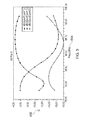
- Figure 5 is a graph comparing a set of S-parameters 502 of the example matched transmission line interconnect versus frequency 504.
- S-parameters for an eWLB plastic waveguide interface with 10mm plastic waveguide in the frequency range between 78 and 102 GHz are shown.
- Port 1 corresponds to the port connected to a dipole antenna and port 2 corresponds to a plastic waveguide port.
- S11 is below -10dB above 86GHz and the S21 is around -4dB at 95 GHz.
- Figure 6 is a graph comparing electrical field strength 602 of the example matched transmission line interconnect over a width 604 of an example plastic waveguide.
- the electrical field strength 602 has been normalized in an x-y cross section at 95GHz.
- the 3mm distance corresponds to the center of the example waveguide.
- Figure 7 is another example of a perspective view of a transmission line interconnect 100 coupled to a transmission line 302.
- An electric field propagation 702 is shown for an eWLB interconnect package and a plastic waveguide 302. As can be seen the electric field 702 is substantially confined in the plastic waveguide 302.
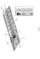
- Figure 8A is one example of a top view of a transmission line interconnect 100 with notches 802 coupled to a transmission line 804.
- Figure 8B is one example of a perspective view of the transmission line interconnect 100 with notches 802 coupled to a transmission line 804 shown in Figure 8A .
- the molding compound 102 (i.e. encapsulant) includes a matched transmission line coupling surface 106 and an un-matched package surface 806.
- the transmission line 804 is coupled to the matched transmission line coupling surface 106 which has been separated from the un-matched package surface 806 by the notches 802.
- notches 802 enable the transmission line coupling surface 106 of the dielectric molding compound 102 to be substantially matched to a cross-sectional area of the transmission line 804.
- the cross-sectional area of the transmission line coupling surface 106 is substantially perpendicular to a longitudinal axis 808 of the transmission line 804.
- the notches 802 enable an example eWLB interconnect package to have cross-sectional surface dimensions which are larger than the transmission line's 804 (e.g. waveguide) cross-sectional area while still forming a matched transmission line coupling surface 106 where the transmission line 804 is coupled to the molding compound 102.
- the interconnect package interface with the waveguide can be modified to allow more flexibility of the waveguide interface (e.g. make larger or smaller interconnect area which substantially matches the waveguide cross-sectional dimensions).
- the notches 802 are air cavities.
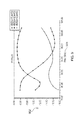
- Figure 9 is a graph comparing a set of S-parameters 902 of an example notched transmission line interconnect versus frequency 904 for a waveguide, such as discussed in Figure 5 .
- Figure 10 is a graph comparing electrical field strength of the example notched transmission line interconnect over a width of an example plastic waveguide, such as discussed in Figure 6 .
- the simulated results shown in Figure 9 , and Figure 10 are almost equal to the results of the matched interconnect package without notches.
- the notches 802 provide an option for connecting interconnect packages that have a different overall cross-sectional areas compared to the waveguide's cross-sectional area.
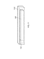
- Figure 11 is one example of a perspective view of a transmission line interconnect 100 coupled to a transmission line 302 within a foam 1100.
- the foam 1100 shields the Figure 11 assembly from selected effects of surrounding electrical and mechanical components (not shown).
- Figure 12A is one example of a top view of a set of transmission line interconnects 1202 and 1204 coupled to transmission lines 1206 and 1208 and including a first set of notches 1210.
- Figure 12B is one example of a perspective view of the set of transmission line interconnects 1202 and 1204 coupled to the transmission lines 1206 and 1208 and including the first set of notches 1210 as shown in Figure 12A .
- the two waveguides 1206 and 1208 are integrated in a same eWLB interconnect package with a transmitter (TX) chip 1212 and a receiver (RX) chip 1214.
- TX transmitter
- RX receiver
- the eWLB package has an un-matched package surface 1216 and a matched transmission line coupling surface 1218.
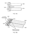
- Figure 13A is one example of a top view of a set of transmission line interconnects 1302 and 1304 coupled to transmission lines 1306 and 1308 and including a second set of notches 1310.
- Figure 13B is one example of a perspective view of a set of transmission line interconnects 1302 and 1304 coupled to transmission lines 1306 and 1308 and including the second set of notches 1310 shown in Figure 13A .
- Figure 14 is one example of a perspective view of a set of encapsulated chips 1402 connected to a set of transmission line interconnects 100 and a set of transmission lines 1404.
- the transmission line interconnects 100 are used for chip-to-chip interconnects between a first device 1406 and a second device 1408, and for board-to-board interconnects between the first device 1406 and another PCB board (not shown).
- the transmission line interconnects 100 can be used to form versatile multi-modality serial links.
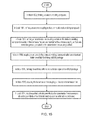
- Figure 15 is one example of a flowchart for manufacturing a transmission line interconnect.
- the method 1500 begins in block 1502, by forming a dielectric molding compound.
- block 1504 defining an antenna coupling surface on the dielectric molding compound.
- block 1506 defining a transmission line coupling surface on the dielectric molding compound whereby millimeter wave frequencies received at the antenna coupling surface are electromagnetically coupled to the transmission line coupling surface.
- block 1508 coupling an antenna to the dielectric molding compound within an embedded Wafer Level Ball Grid Array (eWLB) package.
- Block 1510 forming the antenna within a redistribution layer of the eWLB package.
- Block 1512 coupling the transmission line coupling surface to a transmission line.
- block 1514 matching a first dielectric permittivity of a transmission line to a second dielectric permittivity of the dielectric molding compound to within a tolerance.
- Example embodiments of the material discussed in this specification can be implemented in whole or in part through network, computer, or data based devices and/or services. These may include cloud, internet, intranet, mobile, desktop, processor, look-up table, microcontroller, consumer equipment, infrastructure, or other enabling devices and services. As may be used herein and in the claims, the following non-exclusive definitions are provided.
- one or more blocks or steps discussed herein are automated.
- apparatus, systems, and methods occur automatically.
- automated or automatically mean controlled operation of an apparatus, system, and/or process using computers and/or mechanical/electrical devices without the necessity of human intervention, observation, effort and/or decision.
Landscapes
- Engineering & Computer Science (AREA)
- Physics & Mathematics (AREA)
- Microelectronics & Electronic Packaging (AREA)
- Manufacturing & Machinery (AREA)
- General Physics & Mathematics (AREA)
- Optics & Photonics (AREA)
- Waveguides (AREA)
- Radar Systems Or Details Thereof (AREA)
Abstract
Description
- This specification relates generally to systems and methods for coupling signals and in one example to a transmission line interconnect.
- According to a first aspect, there is provided a transmission line interconnect, comprising: an antenna coupling surface; a transmission line coupling surface; and a dielectric molding compound electromagnetically coupling the antenna coupling surface to the transmission line coupling surface. The transmission line coupling surface may be a waveguide coupling surface. The transmission line interconnect may be coupled to receive and transmit a millimeter wave frequency.
- The interconnect may further comprise a transmission line; and wherein the transmission line coupling surface may be coupled to the transmission line. The transmission line may be a plastic waveguide. The transmission line may have a first dielectric permittivity and the dielectric molding compound may have a second dielectric permittivity which matches the first dielectric permittivity to within a tolerance.
- The interconnect may further comprise a redistribution layer coupled to an antenna; and wherein the antenna coupling surface may be coupled to the redistribution layer. The interconnect may further comprise a transceiver chip coupled to the antenna; and wherein transmission line interconnect may be packaged within an embedded Wafer Level Ball Grid Array (eWLB).
- The interconnect may further comprise a transceiver chip coupled to the antenna; and wherein transmission line interconnect may be packaged within a USB cable. The transmission line coupling surface may include a cross-sectional area substantially matching a transmission line cross-sectional area. The cross-sectional area of the transmission line coupling surface may be substantially perpendicular to a longitudinal axis of the transmission line.
- The interconnect may further comprise a notch; and wherein the dielectric molding compound may include a cross-sectional area substantially perpendicular to a longitudinal axis of the transmission line, and may include the cross-sectional area of the transmission line coupling surface; and wherein the cross-sectional area of the transmission line coupling surface may be separated from the cross-sectional area of the dielectric molding compound by the notch.
- According to a second aspect, there is provided a method of manufacture, for a transmission line interconnect, comprising: forming a dielectric molding compound; defining an antenna coupling surface on the dielectric molding compound; and defining a transmission line coupling surface on the dielectric molding compound whereby millimeter wave frequencies received at the antenna coupling surface are electromagnetically coupled to the transmission line coupling surface.
- The method may further comprise: coupling an antenna to the dielectric molding compound within an embedded Wafer Level Ball Grid Array (eWLB) package. The method may further comprise: forming the antenna within a redistribution layer of the eWLB package. The method may further comprise: coupling the transmission line coupling surface to a transmission line. Forming the dielectric molding compound may include: matching a first dielectric permittivity of a transmission line to a second dielectric permittivity of the dielectric molding compound to within a tolerance.
-
Figure 1 is one example of a side view of a transmission line interconnect. -
Figure 2 is one example of a perspective view of a transmission line interconnect. -
Figure 3 is one example of a perspective view of a transmission line interconnect coupled to a transmission line. -
Figure 4 is a graph comparing a calculated propagation constant for an example matched transmission line interconnect versus frequency. -
Figure 5 is a graph comparing a set of S-parameters of the example matched transmission line interconnect versus frequency. -
Figure 6 is a graph comparing electrical field strength of the example matched transmission line interconnect over a width of an example plastic waveguide. -
Figure 7 is another example of a perspective view of a transmission line interconnect coupled to a transmission line. -
Figure 8A is one example of a top view of a transmission line interconnect with notches coupled to a transmission line. -
Figure 8B is one example of a perspective view of a transmission line interconnect with notches coupled to a transmission line as shown inFigure 8A . -
Figure 9 is a graph comparing a set of S-parameters of an example notched transmission line interconnect versus frequency. -
Figure 10 is a graph comparing electrical field strength of the example notched transmission line interconnect over a width of an example plastic waveguide. -
Figure 11 is one example of a perspective view of a transmission line interconnect coupled to a transmission line within a foam. -
Figure 12A is one example of a top view of a set of transmission line interconnects coupled to transmission lines and including a first set of notches. -
Figure 12B is one example of a perspective view of the set of transmission line interconnects coupled to the transmission lines and including the first set of notches as shown inFigure 12A . -
Figure 13A is one example of a top view of a set of transmission line interconnects coupled to transmission lines and including a second set of notches. -
Figure 13B is one example of a perspective view of the set of transmission line interconnects coupled to the transmission lines and including the second set of notches as shown inFigure 13A . -
Figure 14 is one example of a perspective view of a set of encapsulated chips connected to a set of transmission line interconnects and a set of transmission lines. -
Figure 15 is one example of a flowchart for manufacturing a transmission line interconnect. - While the disclosure is amenable to various modifications and alternative forms, specifics thereof have been shown by way of example in the drawings and will be described in detail. It should be understood, however, that other embodiments, beyond the particular embodiments described, are possible as well. All modifications, equivalents, and alternative embodiments falling within the scope of the appended claims are covered as well.
- High-speed and low-cost interconnects solutions at millimeter-waves (e.g. 30-300 GHz) frequencies require new materials and new connection methods. Plastic waveguides are of lower cost and can efficiently confine electromagnetic waves in the dielectric, eliminating the free space path loss of the wireless connection and the need of electrical-to-optical devices of the fiber optical interconnects.
- In one example an interconnect from a chip to a full duplex plastic (dielectric) waveguide includes a transceiver chip mounted on a printed circuit board (PCB) with two Quasi-Yagi antennas as chip-to-waveguide couplers with a plastic waveguide placed on top of the PCB. The chip can be flip-chip mounted to a coplanar strip or wire-bonded to the antennas on PCB.
- In another example an interconnect a dipole antenna made with two bond wires and an on-chip reflector. The chip area occupied by the antenna and reflector is over 50% of the total chip area. The chip is connected to the PCB with bond wires that can have high inductance at mm-wave frequencies. A plastic waveguide is placed on top of the bond wire antenna.
- Use of bond wires at millimeter-wave (e.g. 30-300 GHz) frequencies however can add to signal loss. A less lossy solution is to connect an antenna directly to a chip. Use of PCB materials can also contribute to signal loss due to a higher dissipation factor of the PCB material, a special mm-wave material is required for the antenna. Also integrating an on-chip antenna reflector can increase costs and size based on the chip area needed for the antenna reflector.
- A transmission line interconnect from a transceiver chip to a waveguide transmission line is now presented. In one example the transmission line interconnect is embodied in an embedded wafer level ball grid array (eWLB) package. The eWLB package includes a transceiver chip, an encapsulant (e.g. molding compound) and an antenna in the redistribution layer (RDL). A transmission line, such as a plastic waveguide (e.g. polypropylene), can also be integrated into the eWLB package, or alternatively abutted to an interface surface on the eWLB package.
- In one example, the antenna is formed from the RDL and is electromagnetically coupled to the waveguide through the encapsulating mold compound. The antenna in the RDL layer excites one or more resonant modes of the waveguide mode.
- The mold compound acts as a dielectric waveguide and induces less signal loss if a dielectric permittivity of the mold compound is as similar to the dielectric permittivity of the plastic waveguide as possible. Matching the interface surface on the eWLB package to that of the waveguide as closely as possible also reduces signal losses. In this example design, the antenna does not require chip area or special PCB materials.
-
Figure 1 is one example of a side view of atransmission line interconnect 100. Thetransmission line interconnect 100 is formed from a dielectric molding compound 102 (aka encapsulant). Themolding compound 102 includes anantenna coupling surface 104 and a transmissionline coupling surface 106. Thedielectric molding compound 102 receives electromagnetic signals at theantenna coupling surface 104 and transmits the electromagnetic signals to the transmissionline coupling surface 106. In one example, thetransmission line interconnect 100 is coupled to receive and transmit millimeter wave frequencies. - The
transmission line interconnect 100 can be packaged in a variety of ways. In one example embodiment thetransmission line interconnect 100 is packaged within an embedded Wafer Level Ball Grid Array (eWLB). The eWLB includes atransceiver chip 108 coupled to one or more redistribution layers 110. The redistribution layers 110 include conductive elements which route electrical contact points on thetransceiver chip 108 to a set of solder bumps 112. The solder bumps 112. In one example embodiment, are connected to a printed circuit board or another electrical device. - The
redistribution layer 110 can also be used to form anantenna 114. Theantenna 114 is positioned near theantenna coupling surface 104 of thedielectric molding compound 102. Theantenna 114 may be directly coupled to thetransceiver chip 108 with a chip toantenna coupler 116. - Electromagnetic coupling performance (e.g. signal losses) of the
transmission line interconnect 100 can be adjusted by varying dimensions of the transmissionline coupling surface 106, varying a dielectric permittivity of themolding compound 102, and varying a position of theantenna 114 with respect to theantenna coupling surface 104. - Example embodiments of the
molding compound 102 can use different encapsulant materials. Epoxy and epoxy blend are one choice for themolding compound 102. Epoxies include organic and inorganic resins, such as used in structural-engineering applications. - Silicone materials are another choice for the
molding compound 102. Because silicone resins are silicon rather than carbon-based, they are not considered organic resins, even though some of their processing and curing regimens are similar to organic resins. Silicone resins are of two primary types: solvent-based and room-temperature-vulcanizable (RTV). Curing is accomplished by different mechanisms, depending on the type. RTVs are cured either by exposure to moisture (room humidity) or by catalyst addition. In contrast, solvent-based silicones are most commonly cured thermally after evaporation of the solvent. Silicones are quite flexible over a range of temperatures (from -65° to 150°C) making them a popular choice for CSPs seeking compliance. - Polyimide is yet another choice for the
molding compound 102. Polyimides are used in die-attach adhesive formulations. Polyimide resins have a high-temperature capability, making them acceptable for high-temperature. -
Figure 2 is one example of a perspective view of atransmission line interconnect 100. The encapsulant 102 (aka molding compound) is this example extends over thetransceiver chip 108. The transmissionline coupling surface 106 includes across-sectional surface area 202. Thecross-sectional surface area 202 in this example is rectangle and includes awidth 204 and aheight 206. -
Figure 3 is one example of a perspective view of atransmission line interconnect 100 coupled to atransmission line 302. Thetransmission line interconnect 100 electromagnetically couples theantenna 114 to thetransmission line 302 through the transmissionline coupling surface 106. In various examples, thetransmission line 302 is: a waveguide formed from plastic or another material. Thetransmission line 302 can either be abutted to themolding compound 102 or a glue or other material may be inserted between thetransmission line 302 and themolding compound 102. - In one example the
transmission line 302 includes a coupling surface cross-sectional area which is substantially matched to thecross-sectional surface area 202 of themolding compound 102. Substantially is herein defined to include, but not be limited to, embodiments having an exact match plus or minus normal manufacturing tolerances. In one example, thewidth 204 andheight 206 of thecross-sectional surface area 202 is selected such that theinterconnect 100 andtransmission line 302 assembly will be optimized for exciting a set of resonant electromagnetic modes at a preselected frequency. - In an example embodiment, the
transmission line 302 has a first dielectric permittivity and thedielectric molding compound 102 has a second dielectric permittivity which could differ from the first dielectric permittivity if only one guided mode is excited. - In another example, the
transmission line 302 is a polypropylene plastic waveguide having a first dielectric permittivity and amold compound 102 having a dielectric permittivity closer to that of the plastic waveguide permittivity than anothermold compound 102 is selected, thereby minimizing signal losses between thetransceiver chip 108 and the waveguide. In an example eWLB package themold compound 102 is an epoxy and the dielectric permittivity is about 3 which is quite close to a dielectric permittivity of polypropylene. - In one example of the
transmission line interconnect 100, a cross-sectional area of the transmissionline coupling surface 106 is substantially perpendicular to alongitudinal axis 304 of thetransmission line 302. - The
transmission line interconnect 100 can be embodied in various devices including: a chip to chip or module to module communication device; a USB cable; a coupling between a storage device and a computer; automotive wired and wireless bus architectures; and RF communication devices. -
Figure 4 is a graph comparing a calculatedpropagation constant 402 for an example matchedtransmission line interconnect 100 versusfrequency 404. In this example, thetransmission line 302 is a 10mm plastic waveguide made from polypropylene having a cross-section of 2.2mm (width) by 0.9mm (height). Thetransmission line interconnect 100 is formed within an eWLB package. The propagation constant is calculated using the Marcatili"s formula. In the frequency band between 78 and 102GHz only one mode can propagate. -
Figure 5 is a graph comparing a set of S-parameters 502 of the example matched transmission line interconnect versusfrequency 504. S-parameters for an eWLB plastic waveguide interface with 10mm plastic waveguide in the frequency range between 78 and 102 GHz are shown. Port 1 corresponds to the port connected to a dipole antenna and port 2 corresponds to a plastic waveguide port. S11 is below -10dB above 86GHz and the S21 is around -4dB at 95 GHz. -
Figure 6 is a graph comparingelectrical field strength 602 of the example matched transmission line interconnect over awidth 604 of an example plastic waveguide. Theelectrical field strength 602 has been normalized in an x-y cross section at 95GHz. The 3mm distance corresponds to the center of the example waveguide. -
Figure 7 is another example of a perspective view of atransmission line interconnect 100 coupled to atransmission line 302. Anelectric field propagation 702 is shown for an eWLB interconnect package and aplastic waveguide 302. As can be seen theelectric field 702 is substantially confined in theplastic waveguide 302. -
Figure 8A is one example of a top view of atransmission line interconnect 100 withnotches 802 coupled to atransmission line 804.Figure 8B is one example of a perspective view of thetransmission line interconnect 100 withnotches 802 coupled to atransmission line 804 shown inFigure 8A . - In the example shown, the molding compound 102 (i.e. encapsulant) includes a matched transmission
line coupling surface 106 and anun-matched package surface 806. Thetransmission line 804 is coupled to the matched transmissionline coupling surface 106 which has been separated from theun-matched package surface 806 by thenotches 802. - These
notches 802 enable the transmissionline coupling surface 106 of thedielectric molding compound 102 to be substantially matched to a cross-sectional area of thetransmission line 804. In this example, the cross-sectional area of the transmissionline coupling surface 106 is substantially perpendicular to alongitudinal axis 808 of thetransmission line 804. - Thus the
notches 802 enable an example eWLB interconnect package to have cross-sectional surface dimensions which are larger than the transmission line's 804 (e.g. waveguide) cross-sectional area while still forming a matched transmissionline coupling surface 106 where thetransmission line 804 is coupled to themolding compound 102. Thus the interconnect package interface with the waveguide can be modified to allow more flexibility of the waveguide interface (e.g. make larger or smaller interconnect area which substantially matches the waveguide cross-sectional dimensions). In one example embodiment thenotches 802 are air cavities. -
Figure 9 is a graph comparing a set of S-parameters 902 of an example notched transmission line interconnect versusfrequency 904 for a waveguide, such as discussed inFigure 5 . -
Figure 10 is a graph comparing electrical field strength of the example notched transmission line interconnect over a width of an example plastic waveguide, such as discussed inFigure 6 . The simulated results shown inFigure 9 , andFigure 10 are almost equal to the results of the matched interconnect package without notches. Thus thenotches 802 provide an option for connecting interconnect packages that have a different overall cross-sectional areas compared to the waveguide's cross-sectional area. -
Figure 11 is one example of a perspective view of atransmission line interconnect 100 coupled to atransmission line 302 within afoam 1100. Thefoam 1100 shields theFigure 11 assembly from selected effects of surrounding electrical and mechanical components (not shown). -
Figure 12A is one example of a top view of a set of transmission line interconnects 1202 and 1204 coupled totransmission lines notches 1210.Figure 12B is one example of a perspective view of the set of transmission line interconnects 1202 and 1204 coupled to thetransmission lines notches 1210 as shown inFigure 12A . - In this example embodiment, the two
waveguides chip 1212 and a receiver (RX)chip 1214. As shown, the eWLB package has anun-matched package surface 1216 and a matched transmissionline coupling surface 1218. -
Figure 13A is one example of a top view of a set of transmission line interconnects 1302 and 1304 coupled totransmission lines notches 1310.Figure 13B is one example of a perspective view of a set of transmission line interconnects 1302 and 1304 coupled totransmission lines notches 1310 shown inFigure 13A . - This example embodiment is similar to that of
Figures 12A and 12B , however thenotches 1310 are of a different configuration. -
Figure 14 is one example of a perspective view of a set of encapsulatedchips 1402 connected to a set of transmission line interconnects 100 and a set oftransmission lines 1404. In this example the transmission line interconnects 100 are used for chip-to-chip interconnects between afirst device 1406 and asecond device 1408, and for board-to-board interconnects between thefirst device 1406 and another PCB board (not shown). Thus the transmission line interconnects 100 can be used to form versatile multi-modality serial links. -
Figure 15 is one example of a flowchart for manufacturing a transmission line interconnect. The method 1500 begins inblock 1502, by forming a dielectric molding compound. Next inblock 1504, defining an antenna coupling surface on the dielectric molding compound. Then inblock 1506, defining a transmission line coupling surface on the dielectric molding compound whereby millimeter wave frequencies received at the antenna coupling surface are electromagnetically coupled to the transmission line coupling surface. - Other example embodiments include,
block 1508, coupling an antenna to the dielectric molding compound within an embedded Wafer Level Ball Grid Array (eWLB) package.Block 1510, forming the antenna within a redistribution layer of the eWLB package.Block 1512, coupling the transmission line coupling surface to a transmission line. And block 1514, matching a first dielectric permittivity of a transmission line to a second dielectric permittivity of the dielectric molding compound to within a tolerance. - The blocks comprising the flowcharts in the above Figures can be executed in any order, unless a specific order is explicitly stated. Also, those skilled in the art will recognize that while one example method embodiment is now discussed, the material in this specification can be combined in a variety of ways to yield other examples as well. The method next discussed is to be understood within a context provided by this and other portions of this detailed description.
- Example embodiments of the material discussed in this specification can be implemented in whole or in part through network, computer, or data based devices and/or services. These may include cloud, internet, intranet, mobile, desktop, processor, look-up table, microcontroller, consumer equipment, infrastructure, or other enabling devices and services. As may be used herein and in the claims, the following non-exclusive definitions are provided.
- In one example, one or more blocks or steps discussed herein are automated. In other words, apparatus, systems, and methods occur automatically. The terms automated or automatically (and like variations thereof) mean controlled operation of an apparatus, system, and/or process using computers and/or mechanical/electrical devices without the necessity of human intervention, observation, effort and/or decision.
- In this specification, example embodiments have been presented in terms of a selected set of details. However, a person of ordinary skill in the art would understand that many other example embodiments may be practiced which include a different selected set of these details. It is intended that the following claims cover all possible example embodiments.
Claims (15)
- A transmission line interconnect, comprising:an antenna coupling surface;a transmission line coupling surface; anda dielectric molding compound electromagnetically coupling the antenna coupling surface to the transmission line coupling surface.
- The interconnect of claim 1, wherein the transmission line coupling surface is a waveguide coupling surface.
- The interconnect of claim 1, wherein the transmission line interconnect is coupled to receive and transmit a millimeter wave frequency.
- The interconnect of claim 1:further comprising a transmission line; andwherein the transmission line coupling surface is coupled to the transmission line.
- The interconnect of claim 4, wherein the transmission line is a plastic waveguide.
- The interconnect of claim 4, wherein the transmission line has a first dielectric permittivity and the dielectric molding compound has a second dielectric permittivity which matches the first dielectric permittivity to within a tolerance.
- The interconnect of claim 1:further comprising a redistribution layer coupled to an antenna; andwherein the antenna coupling surface is coupled to the redistribution layer.
- The interconnect of claim 7:further comprising a transceiver chip coupled to the antenna; andwherein transmission line interconnect is packaged within an embedded Wafer Level Ball Grid Array (eWLB).
- The interconnect of claim 7:further comprising a transceiver chip coupled to the antenna; andwherein transmission line interconnect is packaged within a USB cable.
- The interconnect of claim 1, wherein the transmission line coupling surface includes a cross-sectional area substantially matching a transmission line cross-sectional area.
- The interconnect of claim 10:further comprising a notch; andwherein the dielectric molding compound includes a cross-sectional area substantially perpendicular to a longitudinal axis of the transmission line, and includes the cross-sectional area of the transmission line coupling surface; andwherein the cross-sectional area of the transmission line coupling surface is separated from the cross-sectional area of the dielectric molding compound by the notch.
- A method of manufacture, for a transmission line interconnect, comprising:forming a dielectric molding compound;defining an antenna coupling surface on the dielectric molding compound; anddefining a transmission line coupling surface on the dielectric molding compound whereby millimeter wave frequencies received at the antenna coupling surface are electromagnetically coupled to the transmission line coupling surface.
- The method of claim 12, further comprising:coupling an antenna to the dielectric molding compound within an embedded Wafer Level Ball Grid Array (eWLB) package.
- The method of claim 13, further comprising:forming the antenna within a redistribution layer of the eWLB package.
- The method of claim 12, further comprising:coupling the transmission line coupling surface to a transmission line.
Applications Claiming Priority (1)
| Application Number | Priority Date | Filing Date | Title |
|---|---|---|---|
| US14/205,029 US9515368B2 (en) | 2014-03-11 | 2014-03-11 | Transmission line interconnect |
Publications (2)
| Publication Number | Publication Date |
|---|---|
| EP2919319A1 true EP2919319A1 (en) | 2015-09-16 |
| EP2919319B1 EP2919319B1 (en) | 2019-09-11 |
Family
ID=52807529
Family Applications (1)
| Application Number | Title | Priority Date | Filing Date |
|---|---|---|---|
| EP15158300.2A Active EP2919319B1 (en) | 2014-03-11 | 2015-03-09 | Transmission line interconnect |
Country Status (3)
| Country | Link |
|---|---|
| US (1) | US9515368B2 (en) |
| EP (1) | EP2919319B1 (en) |
| CN (1) | CN104916892B (en) |
Families Citing this family (11)
| Publication number | Priority date | Publication date | Assignee | Title |
|---|---|---|---|---|
| US9496592B2 (en) * | 2014-03-27 | 2016-11-15 | Intel Corporation | Rack level pre-installed interconnect for enabling cableless server/storage/networking deployment |
| US9450635B2 (en) | 2014-04-03 | 2016-09-20 | Intel Corporation | Cableless connection apparatus and method for communication between chassis |
| US9712339B2 (en) * | 2014-04-24 | 2017-07-18 | Infineon Technologies Ag | Bus architecture and access method for plastic waveguide |
| US9648399B2 (en) | 2014-05-08 | 2017-05-09 | Infineon Technologies Ag | System having plastic waveguides |
| US10992022B2 (en) | 2016-04-01 | 2021-04-27 | Sony Corporation | Microwave antenna apparatus, packing and manufacturing method |
| FR3051303A1 (en) * | 2016-05-13 | 2017-11-17 | Commissariat Energie Atomique | MILLIMETER WAVE TRANSMISSION DEVICE |
| JP6408540B2 (en) * | 2016-12-01 | 2018-10-17 | 太陽誘電株式会社 | Wireless module and wireless module manufacturing method |
| WO2019033608A1 (en) * | 2017-08-18 | 2019-02-21 | 华进半导体封装先导技术研发中心有限公司 | Radar module package and fabrication method therefor |
| US10665560B2 (en) * | 2017-10-27 | 2020-05-26 | Taiwan Semiconductor Manufacturing Company Ltd. | Optical semiconductor package and method for manufacturing the same |
| US10937748B1 (en) * | 2019-09-12 | 2021-03-02 | Huawei Technologies Co., Ltd. | Fan-out transition structure for transmission of mm-Wave signals from IC to PCB via chip-scale packaging |
| CN113851857B (en) * | 2021-08-26 | 2024-01-30 | 电子科技大学 | Inverted transition structure of yagi antenna on W-band chip |
Citations (3)
| Publication number | Priority date | Publication date | Assignee | Title |
|---|---|---|---|---|
| US20110267153A1 (en) * | 2009-02-27 | 2011-11-03 | Mitsubishi Electric Corporation | Waveguide-microstrip line converter |
| US20120068890A1 (en) * | 2010-09-21 | 2012-03-22 | Texas Instruments Incorporated | High speed digital interconnect and method |
| US20130265734A1 (en) * | 2012-04-04 | 2013-10-10 | Texas Instruments Incorporated | Interchip communication using embedded dielectric and metal waveguides |
Family Cites Families (7)
| Publication number | Priority date | Publication date | Assignee | Title |
|---|---|---|---|---|
| US6242984B1 (en) * | 1998-05-18 | 2001-06-05 | Trw Inc. | Monolithic 3D radial power combiner and splitter |
| US6967347B2 (en) * | 2001-05-21 | 2005-11-22 | The Regents Of The University Of Colorado | Terahertz interconnect system and applications |
| US7680464B2 (en) * | 2004-12-30 | 2010-03-16 | Valeo Radar Systems, Inc. | Waveguide—printed wiring board (PWB) interconnection |
| US20090009408A1 (en) * | 2006-06-21 | 2009-01-08 | Broadcom Corporation | Integrated circuit with bonding wire antenna structure and methods for use therewith |
| JP4923975B2 (en) * | 2006-11-21 | 2012-04-25 | ソニー株式会社 | Communication system and communication apparatus |
| JP5374994B2 (en) * | 2008-09-25 | 2013-12-25 | ソニー株式会社 | Millimeter-wave dielectric transmission device |
| JP2012186796A (en) * | 2011-02-18 | 2012-09-27 | Sony Corp | Signal transmission device and electronic apparatus |
-
2014
- 2014-03-11 US US14/205,029 patent/US9515368B2/en active Active
-
2015
- 2015-03-09 EP EP15158300.2A patent/EP2919319B1/en active Active
- 2015-03-10 CN CN201510103531.8A patent/CN104916892B/en active Active
Patent Citations (3)
| Publication number | Priority date | Publication date | Assignee | Title |
|---|---|---|---|---|
| US20110267153A1 (en) * | 2009-02-27 | 2011-11-03 | Mitsubishi Electric Corporation | Waveguide-microstrip line converter |
| US20120068890A1 (en) * | 2010-09-21 | 2012-03-22 | Texas Instruments Incorporated | High speed digital interconnect and method |
| US20130265734A1 (en) * | 2012-04-04 | 2013-10-10 | Texas Instruments Incorporated | Interchip communication using embedded dielectric and metal waveguides |
Non-Patent Citations (1)
| Title |
|---|
| NEMAT DOLATSHA ET AL: "Dielectric waveguide with planar multi-mode excitation for high data-rate chip-to-chip interconnects", 2013 IEEE INTERNATIONAL CONFERENCE ON ULTRA-WIDEBAND (ICUWB), 1 September 2013 (2013-09-01), pages 184 - 188, XP055170498, ISBN: 978-1-47-990969-8, DOI: 10.1109/ICUWB.2013.6663845 * |
Also Published As
| Publication number | Publication date |
|---|---|
| EP2919319B1 (en) | 2019-09-11 |
| CN104916892B (en) | 2018-10-09 |
| CN104916892A (en) | 2015-09-16 |
| US9515368B2 (en) | 2016-12-06 |
| US20150263403A1 (en) | 2015-09-17 |
Similar Documents
| Publication | Publication Date | Title |
|---|---|---|
| EP2919319B1 (en) | Transmission line interconnect | |
| KR102461627B1 (en) | Chip antenna module and electronic device including thereof | |
| KR102486785B1 (en) | Chip antenna module | |
| US9647329B2 (en) | Encapsulated molded package with embedded antenna for high data rate communication using a dielectric waveguide | |
| TWI716838B (en) | Antenna structure and antenna-in-package | |
| CN110071369B (en) | Antenna Devices and Antenna Modules | |
| KR102744540B1 (en) | Microelectronic devices designed with flexible package substrates having distributed stacked antennas for high frequency communication systems | |
| CN101336475B (en) | Electronic device and method of constituting electronic device | |
| JP5556072B2 (en) | Semiconductor device, method of manufacturing the same, and millimeter wave dielectric transmission device | |
| US9172131B2 (en) | Semiconductor structure having aperture antenna | |
| KR20210033461A (en) | Antenna apparatus | |
| US20130194754A1 (en) | Transmission line transition having vertical structure and single chip package using land grip array coupling | |
| US8779564B1 (en) | Semiconductor device with capacitive coupling structure | |
| WO2019075026A1 (en) | Interposer between microelectronic package substrate and dielectric waveguide connector | |
| CN103119714B (en) | Chip-to-chip communication using submillimeter waves and dielectric waveguides | |
| US10833394B2 (en) | Electronic package and method for fabricating the same | |
| KR20150108147A (en) | Radar on a package for millimeter wave and radar assembly using the same | |
| KR102246620B1 (en) | Antenna apparatus | |
| CN109873246B (en) | Antenna device and antenna module | |
| CN110718540A (en) | Semiconductor package with plastic waveguide | |
| EP3712640A1 (en) | Radar sensor in transparent package | |
| KR102420287B1 (en) | Packaged devices with integrated antennas | |
| KR102222943B1 (en) | Chip antenna module | |
| KR20210061577A (en) | Antenna apparatus | |
| CN109873247B (en) | Antenna device and antenna module |
Legal Events
| Date | Code | Title | Description |
|---|---|---|---|
| PUAI | Public reference made under article 153(3) epc to a published international application that has entered the european phase |
Free format text: ORIGINAL CODE: 0009012 |
|
| AK | Designated contracting states |
Kind code of ref document: A1 Designated state(s): AL AT BE BG CH CY CZ DE DK EE ES FI FR GB GR HR HU IE IS IT LI LT LU LV MC MK MT NL NO PL PT RO RS SE SI SK SM TR |
|
| AX | Request for extension of the european patent |
Extension state: BA ME |
|
| 17P | Request for examination filed |
Effective date: 20160316 |
|
| RBV | Designated contracting states (corrected) |
Designated state(s): AL AT BE BG CH CY CZ DE DK EE ES FI FR GB GR HR HU IE IS IT LI LT LU LV MC MK MT NL NO PL PT RO RS SE SI SK SM TR |
|
| STAA | Information on the status of an ep patent application or granted ep patent |
Free format text: STATUS: EXAMINATION IS IN PROGRESS |
|
| 17Q | First examination report despatched |
Effective date: 20180726 |
|
| GRAP | Despatch of communication of intention to grant a patent |
Free format text: ORIGINAL CODE: EPIDOSNIGR1 |
|
| STAA | Information on the status of an ep patent application or granted ep patent |
Free format text: STATUS: GRANT OF PATENT IS INTENDED |
|
| INTG | Intention to grant announced |
Effective date: 20190403 |
|
| GRAS | Grant fee paid |
Free format text: ORIGINAL CODE: EPIDOSNIGR3 |
|
| GRAA | (expected) grant |
Free format text: ORIGINAL CODE: 0009210 |
|
| STAA | Information on the status of an ep patent application or granted ep patent |
Free format text: STATUS: THE PATENT HAS BEEN GRANTED |
|
| AK | Designated contracting states |
Kind code of ref document: B1 Designated state(s): AL AT BE BG CH CY CZ DE DK EE ES FI FR GB GR HR HU IE IS IT LI LT LU LV MC MK MT NL NO PL PT RO RS SE SI SK SM TR |
|
| REG | Reference to a national code |
Ref country code: GB Ref legal event code: FG4D |
|
| REG | Reference to a national code |
Ref country code: CH Ref legal event code: EP |
|
| REG | Reference to a national code |
Ref country code: AT Ref legal event code: REF Ref document number: 1179689 Country of ref document: AT Kind code of ref document: T Effective date: 20190915 |
|
| REG | Reference to a national code |
Ref country code: DE Ref legal event code: R096 Ref document number: 602015037599 Country of ref document: DE Ref country code: IE Ref legal event code: FG4D |
|
| REG | Reference to a national code |
Ref country code: NL Ref legal event code: MP Effective date: 20190911 |
|
| REG | Reference to a national code |
Ref country code: LT Ref legal event code: MG4D |
|
| PG25 | Lapsed in a contracting state [announced via postgrant information from national office to epo] |
Ref country code: FI Free format text: LAPSE BECAUSE OF FAILURE TO SUBMIT A TRANSLATION OF THE DESCRIPTION OR TO PAY THE FEE WITHIN THE PRESCRIBED TIME-LIMIT Effective date: 20190911 Ref country code: LT Free format text: LAPSE BECAUSE OF FAILURE TO SUBMIT A TRANSLATION OF THE DESCRIPTION OR TO PAY THE FEE WITHIN THE PRESCRIBED TIME-LIMIT Effective date: 20190911 Ref country code: BG Free format text: LAPSE BECAUSE OF FAILURE TO SUBMIT A TRANSLATION OF THE DESCRIPTION OR TO PAY THE FEE WITHIN THE PRESCRIBED TIME-LIMIT Effective date: 20191211 Ref country code: NO Free format text: LAPSE BECAUSE OF FAILURE TO SUBMIT A TRANSLATION OF THE DESCRIPTION OR TO PAY THE FEE WITHIN THE PRESCRIBED TIME-LIMIT Effective date: 20191211 Ref country code: HR Free format text: LAPSE BECAUSE OF FAILURE TO SUBMIT A TRANSLATION OF THE DESCRIPTION OR TO PAY THE FEE WITHIN THE PRESCRIBED TIME-LIMIT Effective date: 20190911 Ref country code: SE Free format text: LAPSE BECAUSE OF FAILURE TO SUBMIT A TRANSLATION OF THE DESCRIPTION OR TO PAY THE FEE WITHIN THE PRESCRIBED TIME-LIMIT Effective date: 20190911 |
|
| PG25 | Lapsed in a contracting state [announced via postgrant information from national office to epo] |
Ref country code: RS Free format text: LAPSE BECAUSE OF FAILURE TO SUBMIT A TRANSLATION OF THE DESCRIPTION OR TO PAY THE FEE WITHIN THE PRESCRIBED TIME-LIMIT Effective date: 20190911 Ref country code: GR Free format text: LAPSE BECAUSE OF FAILURE TO SUBMIT A TRANSLATION OF THE DESCRIPTION OR TO PAY THE FEE WITHIN THE PRESCRIBED TIME-LIMIT Effective date: 20191212 Ref country code: AL Free format text: LAPSE BECAUSE OF FAILURE TO SUBMIT A TRANSLATION OF THE DESCRIPTION OR TO PAY THE FEE WITHIN THE PRESCRIBED TIME-LIMIT Effective date: 20190911 Ref country code: ES Free format text: LAPSE BECAUSE OF FAILURE TO SUBMIT A TRANSLATION OF THE DESCRIPTION OR TO PAY THE FEE WITHIN THE PRESCRIBED TIME-LIMIT Effective date: 20190911 Ref country code: LV Free format text: LAPSE BECAUSE OF FAILURE TO SUBMIT A TRANSLATION OF THE DESCRIPTION OR TO PAY THE FEE WITHIN THE PRESCRIBED TIME-LIMIT Effective date: 20190911 |
|
| REG | Reference to a national code |
Ref country code: AT Ref legal event code: MK05 Ref document number: 1179689 Country of ref document: AT Kind code of ref document: T Effective date: 20190911 |
|
| PG25 | Lapsed in a contracting state [announced via postgrant information from national office to epo] |
Ref country code: PL Free format text: LAPSE BECAUSE OF FAILURE TO SUBMIT A TRANSLATION OF THE DESCRIPTION OR TO PAY THE FEE WITHIN THE PRESCRIBED TIME-LIMIT Effective date: 20190911 Ref country code: EE Free format text: LAPSE BECAUSE OF FAILURE TO SUBMIT A TRANSLATION OF THE DESCRIPTION OR TO PAY THE FEE WITHIN THE PRESCRIBED TIME-LIMIT Effective date: 20190911 Ref country code: AT Free format text: LAPSE BECAUSE OF FAILURE TO SUBMIT A TRANSLATION OF THE DESCRIPTION OR TO PAY THE FEE WITHIN THE PRESCRIBED TIME-LIMIT Effective date: 20190911 Ref country code: IT Free format text: LAPSE BECAUSE OF FAILURE TO SUBMIT A TRANSLATION OF THE DESCRIPTION OR TO PAY THE FEE WITHIN THE PRESCRIBED TIME-LIMIT Effective date: 20190911 Ref country code: PT Free format text: LAPSE BECAUSE OF FAILURE TO SUBMIT A TRANSLATION OF THE DESCRIPTION OR TO PAY THE FEE WITHIN THE PRESCRIBED TIME-LIMIT Effective date: 20200113 Ref country code: RO Free format text: LAPSE BECAUSE OF FAILURE TO SUBMIT A TRANSLATION OF THE DESCRIPTION OR TO PAY THE FEE WITHIN THE PRESCRIBED TIME-LIMIT Effective date: 20190911 Ref country code: NL Free format text: LAPSE BECAUSE OF FAILURE TO SUBMIT A TRANSLATION OF THE DESCRIPTION OR TO PAY THE FEE WITHIN THE PRESCRIBED TIME-LIMIT Effective date: 20190911 |
|
| PG25 | Lapsed in a contracting state [announced via postgrant information from national office to epo] |
Ref country code: SK Free format text: LAPSE BECAUSE OF FAILURE TO SUBMIT A TRANSLATION OF THE DESCRIPTION OR TO PAY THE FEE WITHIN THE PRESCRIBED TIME-LIMIT Effective date: 20190911 Ref country code: CZ Free format text: LAPSE BECAUSE OF FAILURE TO SUBMIT A TRANSLATION OF THE DESCRIPTION OR TO PAY THE FEE WITHIN THE PRESCRIBED TIME-LIMIT Effective date: 20190911 Ref country code: IS Free format text: LAPSE BECAUSE OF FAILURE TO SUBMIT A TRANSLATION OF THE DESCRIPTION OR TO PAY THE FEE WITHIN THE PRESCRIBED TIME-LIMIT Effective date: 20200224 Ref country code: SM Free format text: LAPSE BECAUSE OF FAILURE TO SUBMIT A TRANSLATION OF THE DESCRIPTION OR TO PAY THE FEE WITHIN THE PRESCRIBED TIME-LIMIT Effective date: 20190911 |
|
| REG | Reference to a national code |
Ref country code: DE Ref legal event code: R097 Ref document number: 602015037599 Country of ref document: DE |
|
| PLBE | No opposition filed within time limit |
Free format text: ORIGINAL CODE: 0009261 |
|
| STAA | Information on the status of an ep patent application or granted ep patent |
Free format text: STATUS: NO OPPOSITION FILED WITHIN TIME LIMIT |
|
| PG2D | Information on lapse in contracting state deleted |
Ref country code: IS |
|
| PG25 | Lapsed in a contracting state [announced via postgrant information from national office to epo] |
Ref country code: DK Free format text: LAPSE BECAUSE OF FAILURE TO SUBMIT A TRANSLATION OF THE DESCRIPTION OR TO PAY THE FEE WITHIN THE PRESCRIBED TIME-LIMIT Effective date: 20190911 Ref country code: IS Free format text: LAPSE BECAUSE OF FAILURE TO SUBMIT A TRANSLATION OF THE DESCRIPTION OR TO PAY THE FEE WITHIN THE PRESCRIBED TIME-LIMIT Effective date: 20200112 |
|
| 26N | No opposition filed |
Effective date: 20200615 |
|
| PG25 | Lapsed in a contracting state [announced via postgrant information from national office to epo] |
Ref country code: SI Free format text: LAPSE BECAUSE OF FAILURE TO SUBMIT A TRANSLATION OF THE DESCRIPTION OR TO PAY THE FEE WITHIN THE PRESCRIBED TIME-LIMIT Effective date: 20190911 |
|
| PG25 | Lapsed in a contracting state [announced via postgrant information from national office to epo] |
Ref country code: MC Free format text: LAPSE BECAUSE OF FAILURE TO SUBMIT A TRANSLATION OF THE DESCRIPTION OR TO PAY THE FEE WITHIN THE PRESCRIBED TIME-LIMIT Effective date: 20190911 |
|
| REG | Reference to a national code |
Ref country code: CH Ref legal event code: PL |
|
| REG | Reference to a national code |
Ref country code: BE Ref legal event code: MM Effective date: 20200331 |
|
| PG25 | Lapsed in a contracting state [announced via postgrant information from national office to epo] |
Ref country code: LU Free format text: LAPSE BECAUSE OF NON-PAYMENT OF DUE FEES Effective date: 20200309 |
|
| PG25 | Lapsed in a contracting state [announced via postgrant information from national office to epo] |
Ref country code: CH Free format text: LAPSE BECAUSE OF NON-PAYMENT OF DUE FEES Effective date: 20200331 Ref country code: LI Free format text: LAPSE BECAUSE OF NON-PAYMENT OF DUE FEES Effective date: 20200331 Ref country code: IE Free format text: LAPSE BECAUSE OF NON-PAYMENT OF DUE FEES Effective date: 20200309 |
|
| PG25 | Lapsed in a contracting state [announced via postgrant information from national office to epo] |
Ref country code: BE Free format text: LAPSE BECAUSE OF NON-PAYMENT OF DUE FEES Effective date: 20200331 |
|
| PG25 | Lapsed in a contracting state [announced via postgrant information from national office to epo] |
Ref country code: TR Free format text: LAPSE BECAUSE OF FAILURE TO SUBMIT A TRANSLATION OF THE DESCRIPTION OR TO PAY THE FEE WITHIN THE PRESCRIBED TIME-LIMIT Effective date: 20190911 Ref country code: MT Free format text: LAPSE BECAUSE OF FAILURE TO SUBMIT A TRANSLATION OF THE DESCRIPTION OR TO PAY THE FEE WITHIN THE PRESCRIBED TIME-LIMIT Effective date: 20190911 Ref country code: CY Free format text: LAPSE BECAUSE OF FAILURE TO SUBMIT A TRANSLATION OF THE DESCRIPTION OR TO PAY THE FEE WITHIN THE PRESCRIBED TIME-LIMIT Effective date: 20190911 |
|
| PG25 | Lapsed in a contracting state [announced via postgrant information from national office to epo] |
Ref country code: MK Free format text: LAPSE BECAUSE OF FAILURE TO SUBMIT A TRANSLATION OF THE DESCRIPTION OR TO PAY THE FEE WITHIN THE PRESCRIBED TIME-LIMIT Effective date: 20190911 |
|
| P01 | Opt-out of the competence of the unified patent court (upc) registered |
Effective date: 20230725 |
|
| PGFP | Annual fee paid to national office [announced via postgrant information from national office to epo] |
Ref country code: GB Payment date: 20260220 Year of fee payment: 12 |
|
| PGFP | Annual fee paid to national office [announced via postgrant information from national office to epo] |
Ref country code: DE Payment date: 20260219 Year of fee payment: 12 |
|
| PGFP | Annual fee paid to national office [announced via postgrant information from national office to epo] |
Ref country code: FR Payment date: 20260220 Year of fee payment: 12 |