EP2916632A1 - Apparatus for mounting a printed circuit board - Google Patents
Apparatus for mounting a printed circuit board Download PDFInfo
- Publication number
- EP2916632A1 EP2916632A1 EP15157937.2A EP15157937A EP2916632A1 EP 2916632 A1 EP2916632 A1 EP 2916632A1 EP 15157937 A EP15157937 A EP 15157937A EP 2916632 A1 EP2916632 A1 EP 2916632A1
- Authority
- EP
- European Patent Office
- Prior art keywords
- circuit board
- piece
- mounting
- bushing
- deformable elements
- Prior art date
- Legal status (The legal status is an assumption and is not a legal conclusion. Google has not performed a legal analysis and makes no representation as to the accuracy of the status listed.)
- Granted
Links
Images


Classifications
-
- H—ELECTRICITY
- H05—ELECTRIC TECHNIQUES NOT OTHERWISE PROVIDED FOR
- H05K—PRINTED CIRCUITS; CASINGS OR CONSTRUCTIONAL DETAILS OF ELECTRIC APPARATUS; MANUFACTURE OF ASSEMBLAGES OF ELECTRICAL COMPONENTS
- H05K1/00—Printed circuits
- H05K1/02—Details
-
- H—ELECTRICITY
- H05—ELECTRIC TECHNIQUES NOT OTHERWISE PROVIDED FOR
- H05K—PRINTED CIRCUITS; CASINGS OR CONSTRUCTIONAL DETAILS OF ELECTRIC APPARATUS; MANUFACTURE OF ASSEMBLAGES OF ELECTRICAL COMPONENTS
- H05K7/00—Constructional details common to different types of electric apparatus
- H05K7/14—Mounting supporting structure in casing or on frame or rack
- H05K7/1401—Mounting supporting structure in casing or on frame or rack comprising clamping or extracting means
- H05K7/1402—Mounting supporting structure in casing or on frame or rack comprising clamping or extracting means for securing or extracting printed circuit boards
- H05K7/1407—Mounting supporting structure in casing or on frame or rack comprising clamping or extracting means for securing or extracting printed circuit boards by turn-bolt or screw member
-
- H—ELECTRICITY
- H05—ELECTRIC TECHNIQUES NOT OTHERWISE PROVIDED FOR
- H05K—PRINTED CIRCUITS; CASINGS OR CONSTRUCTIONAL DETAILS OF ELECTRIC APPARATUS; MANUFACTURE OF ASSEMBLAGES OF ELECTRICAL COMPONENTS
- H05K1/00—Printed circuits
- H05K1/18—Printed circuits structurally associated with non-printed electric components
-
- H—ELECTRICITY
- H05—ELECTRIC TECHNIQUES NOT OTHERWISE PROVIDED FOR
- H05K—PRINTED CIRCUITS; CASINGS OR CONSTRUCTIONAL DETAILS OF ELECTRIC APPARATUS; MANUFACTURE OF ASSEMBLAGES OF ELECTRICAL COMPONENTS
- H05K5/00—Casings, cabinets or drawers for electric apparatus
- H05K5/0026—Casings, cabinets or drawers for electric apparatus provided with connectors and printed circuit boards [PCB], e.g. automotive electronic control units
- H05K5/0034—Casings, cabinets or drawers for electric apparatus provided with connectors and printed circuit boards [PCB], e.g. automotive electronic control units having an overmolded housing covering the PCB
-
- H—ELECTRICITY
- H05—ELECTRIC TECHNIQUES NOT OTHERWISE PROVIDED FOR
- H05K—PRINTED CIRCUITS; CASINGS OR CONSTRUCTIONAL DETAILS OF ELECTRIC APPARATUS; MANUFACTURE OF ASSEMBLAGES OF ELECTRICAL COMPONENTS
- H05K5/00—Casings, cabinets or drawers for electric apparatus
- H05K5/0026—Casings, cabinets or drawers for electric apparatus provided with connectors and printed circuit boards [PCB], e.g. automotive electronic control units
- H05K5/0073—Casings, cabinets or drawers for electric apparatus provided with connectors and printed circuit boards [PCB], e.g. automotive electronic control units having specific features for mounting the housing on an external structure
-
- H—ELECTRICITY
- H05—ELECTRIC TECHNIQUES NOT OTHERWISE PROVIDED FOR
- H05K—PRINTED CIRCUITS; CASINGS OR CONSTRUCTIONAL DETAILS OF ELECTRIC APPARATUS; MANUFACTURE OF ASSEMBLAGES OF ELECTRICAL COMPONENTS
- H05K5/00—Casings, cabinets or drawers for electric apparatus
- H05K5/0026—Casings, cabinets or drawers for electric apparatus provided with connectors and printed circuit boards [PCB], e.g. automotive electronic control units
- H05K5/0078—Casings, cabinets or drawers for electric apparatus provided with connectors and printed circuit boards [PCB], e.g. automotive electronic control units specially adapted for acceleration sensors, e.g. crash sensors, airbag sensors
-
- H—ELECTRICITY
- H05—ELECTRIC TECHNIQUES NOT OTHERWISE PROVIDED FOR
- H05K—PRINTED CIRCUITS; CASINGS OR CONSTRUCTIONAL DETAILS OF ELECTRIC APPARATUS; MANUFACTURE OF ASSEMBLAGES OF ELECTRICAL COMPONENTS
- H05K5/00—Casings, cabinets or drawers for electric apparatus
- H05K5/02—Details
- H05K5/0217—Mechanical details of casings
- H05K5/0221—Locks; Latches
-
- H—ELECTRICITY
- H05—ELECTRIC TECHNIQUES NOT OTHERWISE PROVIDED FOR
- H05K—PRINTED CIRCUITS; CASINGS OR CONSTRUCTIONAL DETAILS OF ELECTRIC APPARATUS; MANUFACTURE OF ASSEMBLAGES OF ELECTRICAL COMPONENTS
- H05K7/00—Constructional details common to different types of electric apparatus
- H05K7/02—Arrangements of circuit components or wiring on supporting structure
- H05K7/06—Arrangements of circuit components or wiring on supporting structure on insulating boards, e.g. wiring harnesses
- H05K7/08—Arrangements of circuit components or wiring on supporting structure on insulating boards, e.g. wiring harnesses on perforated boards
-
- H—ELECTRICITY
- H05—ELECTRIC TECHNIQUES NOT OTHERWISE PROVIDED FOR
- H05K—PRINTED CIRCUITS; CASINGS OR CONSTRUCTIONAL DETAILS OF ELECTRIC APPARATUS; MANUFACTURE OF ASSEMBLAGES OF ELECTRICAL COMPONENTS
- H05K7/00—Constructional details common to different types of electric apparatus
- H05K7/02—Arrangements of circuit components or wiring on supporting structure
- H05K7/12—Resilient or clamping means for holding component to structure
-
- H—ELECTRICITY
- H05—ELECTRIC TECHNIQUES NOT OTHERWISE PROVIDED FOR
- H05K—PRINTED CIRCUITS; CASINGS OR CONSTRUCTIONAL DETAILS OF ELECTRIC APPARATUS; MANUFACTURE OF ASSEMBLAGES OF ELECTRICAL COMPONENTS
- H05K2201/00—Indexing scheme relating to printed circuits covered by H05K1/00
- H05K2201/09—Shape and layout
- H05K2201/09009—Substrate related
- H05K2201/09063—Holes or slots in insulating substrate not used for electrical connections
-
- H—ELECTRICITY
- H05—ELECTRIC TECHNIQUES NOT OTHERWISE PROVIDED FOR
- H05K—PRINTED CIRCUITS; CASINGS OR CONSTRUCTIONAL DETAILS OF ELECTRIC APPARATUS; MANUFACTURE OF ASSEMBLAGES OF ELECTRICAL COMPONENTS
- H05K2201/00—Indexing scheme relating to printed circuits covered by H05K1/00
- H05K2201/10—Details of components or other objects attached to or integrated in a printed circuit board
- H05K2201/10227—Other objects, e.g. metallic pieces
- H05K2201/10401—Eyelets, i.e. rings inserted into a hole through a circuit board
-
- H—ELECTRICITY
- H05—ELECTRIC TECHNIQUES NOT OTHERWISE PROVIDED FOR
- H05K—PRINTED CIRCUITS; CASINGS OR CONSTRUCTIONAL DETAILS OF ELECTRIC APPARATUS; MANUFACTURE OF ASSEMBLAGES OF ELECTRICAL COMPONENTS
- H05K2201/00—Indexing scheme relating to printed circuits covered by H05K1/00
- H05K2201/10—Details of components or other objects attached to or integrated in a printed circuit board
- H05K2201/10431—Details of mounted components
- H05K2201/1059—Connections made by press-fit insertion
-
- H—ELECTRICITY
- H05—ELECTRIC TECHNIQUES NOT OTHERWISE PROVIDED FOR
- H05K—PRINTED CIRCUITS; CASINGS OR CONSTRUCTIONAL DETAILS OF ELECTRIC APPARATUS; MANUFACTURE OF ASSEMBLAGES OF ELECTRICAL COMPONENTS
- H05K2203/00—Indexing scheme relating to apparatus or processes for manufacturing printed circuits covered by H05K3/00
- H05K2203/13—Moulding and encapsulation; Deposition techniques; Protective layers
- H05K2203/1305—Moulding and encapsulation
- H05K2203/1327—Moulding over PCB locally or completely
-
- Y—GENERAL TAGGING OF NEW TECHNOLOGICAL DEVELOPMENTS; GENERAL TAGGING OF CROSS-SECTIONAL TECHNOLOGIES SPANNING OVER SEVERAL SECTIONS OF THE IPC; TECHNICAL SUBJECTS COVERED BY FORMER USPC CROSS-REFERENCE ART COLLECTIONS [XRACs] AND DIGESTS
- Y10—TECHNICAL SUBJECTS COVERED BY FORMER USPC
- Y10T—TECHNICAL SUBJECTS COVERED BY FORMER US CLASSIFICATION
- Y10T403/00—Joints and connections
- Y10T403/47—Molded joint
- Y10T403/471—And independent connection
-
- Y—GENERAL TAGGING OF NEW TECHNOLOGICAL DEVELOPMENTS; GENERAL TAGGING OF CROSS-SECTIONAL TECHNOLOGIES SPANNING OVER SEVERAL SECTIONS OF THE IPC; TECHNICAL SUBJECTS COVERED BY FORMER USPC CROSS-REFERENCE ART COLLECTIONS [XRACs] AND DIGESTS
- Y10—TECHNICAL SUBJECTS COVERED BY FORMER USPC
- Y10T—TECHNICAL SUBJECTS COVERED BY FORMER US CLASSIFICATION
- Y10T403/00—Joints and connections
- Y10T403/47—Molded joint
- Y10T403/472—Molded joint including mechanical interlock
-
- Y—GENERAL TAGGING OF NEW TECHNOLOGICAL DEVELOPMENTS; GENERAL TAGGING OF CROSS-SECTIONAL TECHNOLOGIES SPANNING OVER SEVERAL SECTIONS OF THE IPC; TECHNICAL SUBJECTS COVERED BY FORMER USPC CROSS-REFERENCE ART COLLECTIONS [XRACs] AND DIGESTS
- Y10—TECHNICAL SUBJECTS COVERED BY FORMER USPC
- Y10T—TECHNICAL SUBJECTS COVERED BY FORMER US CLASSIFICATION
- Y10T403/00—Joints and connections
- Y10T403/49—Member deformed in situ
Definitions
- the present invention is directed to an apparatus for mounting a printed circuit board (“PCB”) to a structure and is particularly directed to a press fit bushing for a PCB used for mounting the PCB to a structure.
- PCB printed circuit board
- PCB's are substrates that hold and interconnect electrical circuit components as part of a larger electrical system.
- PCB's are often mounted into a housing structure designed to hold and protect the PCB and associated circuitry.
- Various ways of mounting the PCB in the house are known such as by using screws or other attachment means. In such mounting arrangements, the screws are directly received through a mounting hole in the PCB and secured to associated screw support structure of the housing. The housing is then, in turn, typically secured to another structure such as a mounting location within a vehicle.
- a circuit board mounting arrangement including a circuit board and a press fit mounting bushing including a cylindrical inner piece and an outer piece secured to the inner piece.
- the outer piece has a plurality of radially projecting, deformable elements and the circuit board has a cylindrical opening having a diameter less than an outer diameter of the radially projecting deformable elements.
- the deformable elements deform when the mounting bushing is pushed into the cylindrical opening of the circuit board so as to hold the mounting bushing to the circuit board.
- the circuit board and press fit bushing are then overmolded.
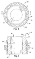
- a two piece press fit mounting bushing 20 is shown used for mounting a printed circuit board ("PCB") 22 to a structure.
- the two piece mounting bushing 20 includes an inner cylindrical piece 26 having a through bore 28.
- the inner cylindrical piece 26 is made from metal.
- a portion 30 of the outer wall 32 of the inner piece 26 has a knurled surface or, at least, a surface that has a rough texture.
- the inner piece 26 could be formed through machining, cold forming, or other metal forming processes with the knurled surface.
- the two piece mounting bushing 20 further includes an outer piece 36 that circumferentially covers at least an axial portion of the inner cylindrical piece 26 commensurate with the knurled surface.
- the outer piece 36 is made from plastic and is molded to the outer wall 32 and in contact with the knurled portion 30 so as to be adhered and fixed to the inner piece 26.
- the knurled surface, or otherwise textured surface of the inner piece provides mechanical retention between the outer piece 36 and the inner piece 26.
- the outer piece being plastic electrically isolates the inner piece from the printed circuit board 22.
- the outer piece 36 of the two piece bushing 20 includes a main body portion 40 and a plurality of radially extending retaining members 42 circumferentially and equally spaced around the main body portion 40.
- the radially extending retaining members 42 are substantially V-shaped in cross section but could take other forms.
- the retaining ring 50 radially extends outward from the main body portion 40.
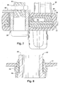
- a first end 52 of the two piece mounting bushing 20 is inserted, i.e., press fit, into an opening 56 of the PCB 22.
- the outside radial diameter of the radially extending retaining members 42 is slightly greater than the diameter of the opening 56 of the PCB 22 such that the bushing 20 must be press fit into the opening with sufficient force applied against end 58. Force would be continuously applied until the retaining ring 50 contacts the PCB 22.
- the radially extending retaining members 42 deform slightly and form a tight press fit engagement, i.e., interference fit, with the PCB 22.
- a bolt may then be inserted through the opening 28 so as to secure the PCB 22 to a mounting structure via a nut on the end of the bolt.
- the press fit mounting bushing were made entirely of metal, such a bushing would cause stress in the PCB board when inserted into the PCB. Also, if the PCB would include a plurality of all metal bushings, the accumulated stress caused by the metal bushings could result in a bowing of the PCB.
- the PCB 22 includes circuitry 64 mounted to the PCB 22.
- the circuitry 64 could include vehicle crash sensors such as an accelerometer or a pressure sensor.
- the bushing 20 is mounted to the PCB 22 as described above with regard to Figs. 1-6 .
- the two piece bushing 20 is press fit into the circuit board 22 as described above prior to an overmolding process.
- a soft plastic material 68 is molded over the circuitry 64 and a portion of the PCB 22.
- a hard plastic material 72 is then overmolded the soft plastic material 68, the exposed portions of the PCB 22 and the two piece bushing 20.
- the hard plastic material forms a rigid mounting case 74 that is formed, i.e., molded, into any desired shape.
- the rigid mounting case 78 is then, in turn, secured to a mounting structure 80, such as a mounting beam in a vehicle, using a bolt 82 and associated nut 84 through the two piece bushing 20.
- FIG. 8 another example embodiment is shown of the present invention using a modified two piece press fit bushing 20' for mounting to a PCB 22.
- the bushing 20' has an inner member 26' made of metal and outer plastic member 36' secured to a knurled portion of the inner member in a similar manner as described above.
- the inner member 26' includes a stepped flange portion 90 that provides an additional contact surface to enhance the retention characteristics between the inner member 26' and the outer member 36' of the two piece bushing 20'.
Landscapes
- Engineering & Computer Science (AREA)
- Microelectronics & Electronic Packaging (AREA)
- Multi-Conductor Connections (AREA)
- Mounting Of Printed Circuit Boards And The Like (AREA)
- Casings For Electric Apparatus (AREA)
Abstract
Description
- The present invention is directed to an apparatus for mounting a printed circuit board ("PCB") to a structure and is particularly directed to a press fit bushing for a PCB used for mounting the PCB to a structure.
- PCB's are substrates that hold and interconnect electrical circuit components as part of a larger electrical system. PCB's are often mounted into a housing structure designed to hold and protect the PCB and associated circuitry. Various ways of mounting the PCB in the house are known such as by using screws or other attachment means. In such mounting arrangements, the screws are directly received through a mounting hole in the PCB and secured to associated screw support structure of the housing. The housing is then, in turn, typically secured to another structure such as a mounting location within a vehicle.
- In accordance with one embodiment of the present invention, a circuit board mounting arrangement is provided including a circuit board and a press fit mounting bushing including a cylindrical inner piece and an outer piece secured to the inner piece. The outer piece has a plurality of radially projecting, deformable elements and the circuit board has a cylindrical opening having a diameter less than an outer diameter of the radially projecting deformable elements. The deformable elements deform when the mounting bushing is pushed into the cylindrical opening of the circuit board so as to hold the mounting bushing to the circuit board. The circuit board and press fit bushing are then overmolded.
- The foregoing and other features and advantages of the present invention will become apparent to those skilled in the art to which the present invention relates upon reading the following description with reference to the accompanying drawings, in which:
-
Fig. 1 is a perspective view of a press fit mounting bushing made in accordance with one example embodiment of the present invention that is used for mounting a printed circuit board to a mounting structure; -
Fig. 2 is side elevation view of the mounting bushing ofFig. 1 ; -
Fig. 3 is a top plan view of the mounting bushing ofFig. 1 ; -
Fig. 4 is a cross-section view of the bushing ofFig. 3 taken along the line 4-4; -
Fig. 5 is a perspective view of the bushing ofFig. 1 press fit into a printed circuit board; -
Fig. 6 is a cross-sectional view of the bushing ofFig. 5 taken along the line 6-6; -
Fig. 7 is a cross-section view of the printed circuit board mounting arrangement of the present invention using the bushing ofFig, 1 showing the circuit board mounted inside of a housing; and -
Fig. 8 is a side cross-sectional view of a press fit mounting bushing in accordance with another embodiment of the present invention. - Referring to
Figs. 1-6 , a two piece press fit mounting bushing 20 is shown used for mounting a printed circuit board ("PCB") 22 to a structure. The two piece mounting bushing 20 includes an innercylindrical piece 26 having a throughbore 28. In accordance with one example embodiment of the present invention, the innercylindrical piece 26 is made from metal. Aportion 30 of theouter wall 32 of theinner piece 26 has a knurled surface or, at least, a surface that has a rough texture. Theinner piece 26 could be formed through machining, cold forming, or other metal forming processes with the knurled surface. - The two piece mounting bushing 20 further includes an
outer piece 36 that circumferentially covers at least an axial portion of the innercylindrical piece 26 commensurate with the knurled surface. In accordance with one example embodiment of the present invention, theouter piece 36 is made from plastic and is molded to theouter wall 32 and in contact with theknurled portion 30 so as to be adhered and fixed to theinner piece 26. The knurled surface, or otherwise textured surface of the inner piece, provides mechanical retention between theouter piece 36 and theinner piece 26. The outer piece being plastic electrically isolates the inner piece from the printedcircuit board 22. - The
outer piece 36 of the two piece bushing 20 includes amain body portion 40 and a plurality of radially extending retainingmembers 42 circumferentially and equally spaced around themain body portion 40. The radially extending retainingmembers 42 are substantially V-shaped in cross section but could take other forms. Theretaining ring 50 radially extends outward from themain body portion 40. - A
first end 52 of the two piece mounting bushing 20 is inserted, i.e., press fit, into anopening 56 of thePCB 22. The outside radial diameter of the radially extending retainingmembers 42 is slightly greater than the diameter of theopening 56 of thePCB 22 such that thebushing 20 must be press fit into the opening with sufficient force applied againstend 58. Force would be continuously applied until theretaining ring 50 contacts the PCB 22. During the process of inserting thebushing 20 into thePCB 22, the radially extending retainingmembers 42 deform slightly and form a tight press fit engagement, i.e., interference fit, with thePCB 22. A bolt may then be inserted through theopening 28 so as to secure thePCB 22 to a mounting structure via a nut on the end of the bolt. - If the press fit mounting bushing were made entirely of metal, such a bushing would cause stress in the PCB board when inserted into the PCB. Also, if the PCB would include a plurality of all metal bushings, the accumulated stress caused by the metal bushings could result in a bowing of the PCB.
- Referring to
Fig. 7 , a completedmounting arrangement 60 for aPCB 22 in accordance with one embodiment of the present invention is shown. ThePCB 22 includescircuitry 64 mounted to thePCB 22. In a vehicle application, thecircuitry 64 could include vehicle crash sensors such as an accelerometer or a pressure sensor. Thebushing 20 is mounted to thePCB 22 as described above with regard toFigs. 1-6 . The two piece bushing 20 is press fit into thecircuit board 22 as described above prior to an overmolding process. First, a softplastic material 68 is molded over thecircuitry 64 and a portion of thePCB 22. A hardplastic material 72 is then overmolded the softplastic material 68, the exposed portions of thePCB 22 and the two piece bushing 20. The hard plastic material forms arigid mounting case 74 that is formed, i.e., molded, into any desired shape. The rigid mounting case 78 is then, in turn, secured to amounting structure 80, such as a mounting beam in a vehicle, using abolt 82 and associatednut 84 through the two piece bushing 20. - An overmolding process showing the soft inner layer and hard outer layer for a vehicle crash sensor arrangement is shown and described in U.S. Patent Application Publication
US2011/0107835A1 which is hereby fully incorporated herein by reference. - Referring to
Fig. 8 , another example embodiment is shown of the present invention using a modified two piece press fit bushing 20' for mounting to aPCB 22. The bushing 20' has an inner member 26' made of metal and outer plastic member 36' secured to a knurled portion of the inner member in a similar manner as described above. With this embodiment, the inner member 26' includes astepped flange portion 90 that provides an additional contact surface to enhance the retention characteristics between the inner member 26' and the outer member 36' of the two piece bushing 20'. - From the above description of the invention, those skilled in the art will perceive improvements, changes and modifications. For example, the retention members have been described, in accordance with one example embodiment, as being V-shaped in cross section. Other shapes or patterns could also be used. Such improvements, changes and modifications within the skill of the art are intended to be covered by the appended claims.
Claims (10)
- A circuit board mounting arrangement comprising:a circuit board; anda press fit mounting bushing including a cylindrical inner piece and an outer piece secured to said inner piece, said outer piece having a plurality of radially projecting, deformable elements, said circuit board having a cylindrical opening having a diameter less than an outer diameter of said radially projecting deformable elements of said outer layer, said deformable elements deforming when said mounting bushing is pushed into said cylindrical opening of said circuit board so as to hold said mounting bushing to said circuit board.
- The circuit board mounting arrangement of claim 1 wherein said cylindrical inner piece is made from metal and has a knurled outer surface and wherein said outer piece is plastic and is secured to said knurled surface of said cylindrical inner piece.
- The circuit board mounting arrangement of claim 2 wherein said circuit board and said press fit mounting bushing are overmolded with plastic material so as to protect any circuitry on said mounting board and to provide a housing.
- The circuit board mounting arrangement of claim 3 wherein said housing is mounted to a structure using a threaded fastener.
- The circuit board mounting arrangement of claim 2 wherein said outer piece is molded to said inner piece.
- The circuit board mounting arrangement of claim 1 wherein said deformable elements are generally V-shaped in cross section.
- A circuit board mounting arrangement comprising:a circuit board; anda press fit mounting bushing including a cylindrical inner piece and an outer piece secured to said inner piece, said outer piece having a plurality of radially projecting, deformable elements, said circuit board having a cylindrical opening having a diameter less than an outer diameter of said radially projecting deformable elements of said outer layer, said deformable elements deforming when said mounting bushing is pushed into said cylindrical opening of said circuit board so as to hold said mounting bushing to said circuit board, wherein said cylindrical inner piece is made from metal and has a knurled outer surface and a stepped surface and wherein said outer piece is plastic and is secured to said knurled surface and to said stepped surface of said cylindrical inner piece.
- The circuit board mounting arrangement of claim 7 wherein said cylindrical inner piece is made from metal and said outer piece is plastic.
- The circuit board mounting arrangement of claim 8 wherein said outer piece is molded to said inner piece.
- The circuit board mounting arrangement of claim 7 wherein said deformable elements are generally V-shaped in cross section.
Applications Claiming Priority (1)
| Application Number | Priority Date | Filing Date | Title |
|---|---|---|---|
| US14/199,294 US9648721B2 (en) | 2014-03-06 | 2014-03-06 | Apparatus for mounting a printed circuit board |
Publications (2)
| Publication Number | Publication Date |
|---|---|
| EP2916632A1 true EP2916632A1 (en) | 2015-09-09 |
| EP2916632B1 EP2916632B1 (en) | 2023-04-05 |
Family
ID=53180500
Family Applications (1)
| Application Number | Title | Priority Date | Filing Date |
|---|---|---|---|
| EP15157937.2A Active EP2916632B1 (en) | 2014-03-06 | 2015-03-06 | Apparatus for mounting a printed circuit board |
Country Status (4)
| Country | Link |
|---|---|
| US (1) | US9648721B2 (en) |
| EP (1) | EP2916632B1 (en) |
| KR (1) | KR101702746B1 (en) |
| CN (1) | CN105101722B (en) |
Cited By (2)
| Publication number | Priority date | Publication date | Assignee | Title |
|---|---|---|---|---|
| WO2018215555A3 (en) * | 2017-05-25 | 2019-01-10 | Valeo Comfort And Driving Assistance | Printed circuit board assembly and packaging method thereof, and motor vehicle comprising said assembly |
| US11525482B2 (en) * | 2018-04-27 | 2022-12-13 | Bayerische Motoren Werke Aktiengesellschaft | Method for producing a shaft-hub connection, and motor vehicle shaft having such a connection |
Families Citing this family (1)
| Publication number | Priority date | Publication date | Assignee | Title |
|---|---|---|---|---|
| JP6915555B2 (en) * | 2018-01-23 | 2021-08-04 | トヨタ自動車株式会社 | Joining structure of parts |
Citations (4)
| Publication number | Priority date | Publication date | Assignee | Title |
|---|---|---|---|---|
| US5363276A (en) * | 1993-09-01 | 1994-11-08 | Ncr Corporation | Apparatus for containing and supporting electronic components |
| US5879115A (en) * | 1992-05-22 | 1999-03-09 | Unimation, Inc. | Method and insert for connecting components to plastic members |
| US6180883B1 (en) * | 1999-02-08 | 2001-01-30 | General Motors Corporation | Cast in situ retention features for a press fit assembly |
| US20110107835A1 (en) | 2008-07-28 | 2011-05-12 | Curt Douglas Campbell | Method and apparatus for packaging crash sensors |
Family Cites Families (9)
| Publication number | Priority date | Publication date | Assignee | Title |
|---|---|---|---|---|
| US4521004A (en) * | 1982-10-27 | 1985-06-04 | Caldwell William F | Vibration-isolating mounting with load-directing chamfer |
| DE3539361A1 (en) * | 1985-11-06 | 1987-05-14 | Siemens Ag | Connecting element for electronic modules of sandwich construction |
| US6395985B1 (en) * | 1999-11-23 | 2002-05-28 | Sapco | Sealed electrical terminal with anti-rotation locking system |
| EP1443331A3 (en) | 2003-02-03 | 2005-10-12 | Denso Corporation | Sensor device and ceramic package for mounting electronic components |
| CN1816700A (en) * | 2003-07-03 | 2006-08-09 | 库博标准汽车配件有限公司 | Plastic quick-snap centerbearing isolator mount and method of manufacturing and assembling same |
| KR100662099B1 (en) | 2006-05-04 | 2006-12-27 | 삼양기전(주) | Rebar connector |
| DE102007036418A1 (en) * | 2007-08-02 | 2008-04-30 | Daimler Ag | Electronic component e.g. printed circuit board, mounting arrangement, has spraying pin that engages in spraying area of pivot in arrangement and presses spraying noses radially inward against inner wall of passage opening of component |
| DE102008000442A1 (en) * | 2008-02-29 | 2009-09-03 | Robert Bosch Gmbh | board assembly |
| US8156797B2 (en) * | 2008-07-28 | 2012-04-17 | Trw Automotive U.S. Llc | Method and apparatus for overmolding a tire pressure monitor sensor |
-
2014
- 2014-03-06 US US14/199,294 patent/US9648721B2/en active Active
-
2015
- 2015-03-02 KR KR1020150028886A patent/KR101702746B1/en active Active
- 2015-03-05 CN CN201510097932.7A patent/CN105101722B/en active Active
- 2015-03-06 EP EP15157937.2A patent/EP2916632B1/en active Active
Patent Citations (4)
| Publication number | Priority date | Publication date | Assignee | Title |
|---|---|---|---|---|
| US5879115A (en) * | 1992-05-22 | 1999-03-09 | Unimation, Inc. | Method and insert for connecting components to plastic members |
| US5363276A (en) * | 1993-09-01 | 1994-11-08 | Ncr Corporation | Apparatus for containing and supporting electronic components |
| US6180883B1 (en) * | 1999-02-08 | 2001-01-30 | General Motors Corporation | Cast in situ retention features for a press fit assembly |
| US20110107835A1 (en) | 2008-07-28 | 2011-05-12 | Curt Douglas Campbell | Method and apparatus for packaging crash sensors |
Cited By (3)
| Publication number | Priority date | Publication date | Assignee | Title |
|---|---|---|---|---|
| WO2018215555A3 (en) * | 2017-05-25 | 2019-01-10 | Valeo Comfort And Driving Assistance | Printed circuit board assembly and packaging method thereof, and motor vehicle comprising said assembly |
| US11284524B2 (en) | 2017-05-25 | 2022-03-22 | Valeo Comfort And Driving Assistance | Printed circuit board assembly and packaging method thereof, and motor vehicle |
| US11525482B2 (en) * | 2018-04-27 | 2022-12-13 | Bayerische Motoren Werke Aktiengesellschaft | Method for producing a shaft-hub connection, and motor vehicle shaft having such a connection |
Also Published As
| Publication number | Publication date |
|---|---|
| CN105101722A (en) | 2015-11-25 |
| CN105101722B (en) | 2018-05-15 |
| KR101702746B1 (en) | 2017-02-06 |
| EP2916632B1 (en) | 2023-04-05 |
| US9648721B2 (en) | 2017-05-09 |
| KR20150105215A (en) | 2015-09-16 |
| US20150257248A1 (en) | 2015-09-10 |
Similar Documents
| Publication | Publication Date | Title |
|---|---|---|
| CN107781270B (en) | Screw with washer | |
| EP2518282A3 (en) | External threaded mount attachment for fan case | |
| EP2916632A1 (en) | Apparatus for mounting a printed circuit board | |
| CN103104581A (en) | Screw assembly element | |
| US9755367B2 (en) | Charging inlet | |
| JP5892087B2 (en) | Electronic control unit for vehicle and manufacturing method thereof | |
| KR20140021607A (en) | Self-centring cage nut | |
| US7161087B2 (en) | Module assembly with mounting integrity detection including deformable washer | |
| EP2472234A3 (en) | Sensing assembly components and methods of assembling, mounting and orientating same | |
| DE102016205240B3 (en) | Method of manufacturing an ultrasonic sensor and ultrasonic sensor | |
| EP4234962A3 (en) | Grain bin system and method of installing an external stiffener to a sidewall of a grain bin | |
| CN104507754B (en) | Mounted Antenna Devices for Vehicles | |
| EP2674764A1 (en) | Method for producing a sensor unit, sensor unit and instrumented bearing comprising such a sensor unit | |
| KR20170075989A (en) | Protector of dash grommet for vehicle | |
| US9696334B2 (en) | Wheel speed sensor | |
| EP2927658B1 (en) | Physical quantity measuring device | |
| US20160076567A1 (en) | Fastening device | |
| DE102007042594A1 (en) | Electrical device for motor vehicle, has housing surrounding metal bush, which includes opening for passage of screw bolt for fastening device at assembly surface, where sensor arrangement is directly connected with metal bush | |
| CN211128485U (en) | Electronic control device and substrate applicable to same | |
| US9831651B2 (en) | Cable fastening device | |
| JP2016058704A (en) | Shield case | |
| CN204586614U (en) | A kind of blanking cover of automobile armrest | |
| JP6285328B2 (en) | Wire harness fixing structure | |
| JP5921941B2 (en) | Connector, satellite converter | |
| EP3713793A2 (en) | A screw cap |
Legal Events
| Date | Code | Title | Description |
|---|---|---|---|
| PUAI | Public reference made under article 153(3) epc to a published international application that has entered the european phase |
Free format text: ORIGINAL CODE: 0009012 |
|
| AK | Designated contracting states |
Kind code of ref document: A1 Designated state(s): AL AT BE BG CH CY CZ DE DK EE ES FI FR GB GR HR HU IE IS IT LI LT LU LV MC MK MT NL NO PL PT RO RS SE SI SK SM TR |
|
| AX | Request for extension of the european patent |
Extension state: BA ME |
|
| 17P | Request for examination filed |
Effective date: 20160309 |
|
| RBV | Designated contracting states (corrected) |
Designated state(s): AL AT BE BG CH CY CZ DE DK EE ES FI FR GB GR HR HU IE IS IT LI LT LU LV MC MK MT NL NO PL PT RO RS SE SI SK SM TR |
|
| STAA | Information on the status of an ep patent application or granted ep patent |
Free format text: STATUS: EXAMINATION IS IN PROGRESS |
|
| 17Q | First examination report despatched |
Effective date: 20190614 |
|
| GRAP | Despatch of communication of intention to grant a patent |
Free format text: ORIGINAL CODE: EPIDOSNIGR1 |
|
| STAA | Information on the status of an ep patent application or granted ep patent |
Free format text: STATUS: GRANT OF PATENT IS INTENDED |
|
| INTG | Intention to grant announced |
Effective date: 20221019 |
|
| GRAS | Grant fee paid |
Free format text: ORIGINAL CODE: EPIDOSNIGR3 |
|
| GRAA | (expected) grant |
Free format text: ORIGINAL CODE: 0009210 |
|
| STAA | Information on the status of an ep patent application or granted ep patent |
Free format text: STATUS: THE PATENT HAS BEEN GRANTED |
|
| AK | Designated contracting states |
Kind code of ref document: B1 Designated state(s): AL AT BE BG CH CY CZ DE DK EE ES FI FR GB GR HR HU IE IS IT LI LT LU LV MC MK MT NL NO PL PT RO RS SE SI SK SM TR |
|
| REG | Reference to a national code |
Ref country code: GB Ref legal event code: FG4D |
|
| REG | Reference to a national code |
Ref country code: DE Ref legal event code: R096 Ref document number: 602015083024 Country of ref document: DE |
|
| REG | Reference to a national code |
Ref country code: CH Ref legal event code: EP |
|
| REG | Reference to a national code |
Ref country code: AT Ref legal event code: REF Ref document number: 1559266 Country of ref document: AT Kind code of ref document: T Effective date: 20230415 |
|
| REG | Reference to a national code |
Ref country code: IE Ref legal event code: FG4D |
|
| P01 | Opt-out of the competence of the unified patent court (upc) registered |
Effective date: 20230524 |
|
| REG | Reference to a national code |
Ref country code: LT Ref legal event code: MG9D |
|
| REG | Reference to a national code |
Ref country code: NL Ref legal event code: MP Effective date: 20230405 |
|
| REG | Reference to a national code |
Ref country code: AT Ref legal event code: MK05 Ref document number: 1559266 Country of ref document: AT Kind code of ref document: T Effective date: 20230405 |
|
| PG25 | Lapsed in a contracting state [announced via postgrant information from national office to epo] |
Ref country code: NL Free format text: LAPSE BECAUSE OF FAILURE TO SUBMIT A TRANSLATION OF THE DESCRIPTION OR TO PAY THE FEE WITHIN THE PRESCRIBED TIME-LIMIT Effective date: 20230405 |
|
| PG25 | Lapsed in a contracting state [announced via postgrant information from national office to epo] |
Ref country code: SE Free format text: LAPSE BECAUSE OF FAILURE TO SUBMIT A TRANSLATION OF THE DESCRIPTION OR TO PAY THE FEE WITHIN THE PRESCRIBED TIME-LIMIT Effective date: 20230405 Ref country code: PT Free format text: LAPSE BECAUSE OF FAILURE TO SUBMIT A TRANSLATION OF THE DESCRIPTION OR TO PAY THE FEE WITHIN THE PRESCRIBED TIME-LIMIT Effective date: 20230807 Ref country code: NO Free format text: LAPSE BECAUSE OF FAILURE TO SUBMIT A TRANSLATION OF THE DESCRIPTION OR TO PAY THE FEE WITHIN THE PRESCRIBED TIME-LIMIT Effective date: 20230705 Ref country code: ES Free format text: LAPSE BECAUSE OF FAILURE TO SUBMIT A TRANSLATION OF THE DESCRIPTION OR TO PAY THE FEE WITHIN THE PRESCRIBED TIME-LIMIT Effective date: 20230405 Ref country code: AT Free format text: LAPSE BECAUSE OF FAILURE TO SUBMIT A TRANSLATION OF THE DESCRIPTION OR TO PAY THE FEE WITHIN THE PRESCRIBED TIME-LIMIT Effective date: 20230405 |
|
| PG25 | Lapsed in a contracting state [announced via postgrant information from national office to epo] |
Ref country code: RS Free format text: LAPSE BECAUSE OF FAILURE TO SUBMIT A TRANSLATION OF THE DESCRIPTION OR TO PAY THE FEE WITHIN THE PRESCRIBED TIME-LIMIT Effective date: 20230405 Ref country code: PL Free format text: LAPSE BECAUSE OF FAILURE TO SUBMIT A TRANSLATION OF THE DESCRIPTION OR TO PAY THE FEE WITHIN THE PRESCRIBED TIME-LIMIT Effective date: 20230405 Ref country code: LV Free format text: LAPSE BECAUSE OF FAILURE TO SUBMIT A TRANSLATION OF THE DESCRIPTION OR TO PAY THE FEE WITHIN THE PRESCRIBED TIME-LIMIT Effective date: 20230405 Ref country code: LT Free format text: LAPSE BECAUSE OF FAILURE TO SUBMIT A TRANSLATION OF THE DESCRIPTION OR TO PAY THE FEE WITHIN THE PRESCRIBED TIME-LIMIT Effective date: 20230405 Ref country code: IS Free format text: LAPSE BECAUSE OF FAILURE TO SUBMIT A TRANSLATION OF THE DESCRIPTION OR TO PAY THE FEE WITHIN THE PRESCRIBED TIME-LIMIT Effective date: 20230805 Ref country code: HR Free format text: LAPSE BECAUSE OF FAILURE TO SUBMIT A TRANSLATION OF THE DESCRIPTION OR TO PAY THE FEE WITHIN THE PRESCRIBED TIME-LIMIT Effective date: 20230405 Ref country code: GR Free format text: LAPSE BECAUSE OF FAILURE TO SUBMIT A TRANSLATION OF THE DESCRIPTION OR TO PAY THE FEE WITHIN THE PRESCRIBED TIME-LIMIT Effective date: 20230706 Ref country code: AL Free format text: LAPSE BECAUSE OF FAILURE TO SUBMIT A TRANSLATION OF THE DESCRIPTION OR TO PAY THE FEE WITHIN THE PRESCRIBED TIME-LIMIT Effective date: 20230405 |
|
| PG25 | Lapsed in a contracting state [announced via postgrant information from national office to epo] |
Ref country code: FI Free format text: LAPSE BECAUSE OF FAILURE TO SUBMIT A TRANSLATION OF THE DESCRIPTION OR TO PAY THE FEE WITHIN THE PRESCRIBED TIME-LIMIT Effective date: 20230405 |
|
| REG | Reference to a national code |
Ref country code: DE Ref legal event code: R097 Ref document number: 602015083024 Country of ref document: DE |
|
| PG25 | Lapsed in a contracting state [announced via postgrant information from national office to epo] |
Ref country code: SK Free format text: LAPSE BECAUSE OF FAILURE TO SUBMIT A TRANSLATION OF THE DESCRIPTION OR TO PAY THE FEE WITHIN THE PRESCRIBED TIME-LIMIT Effective date: 20230405 |
|
| PG25 | Lapsed in a contracting state [announced via postgrant information from national office to epo] |
Ref country code: SM Free format text: LAPSE BECAUSE OF FAILURE TO SUBMIT A TRANSLATION OF THE DESCRIPTION OR TO PAY THE FEE WITHIN THE PRESCRIBED TIME-LIMIT Effective date: 20230405 Ref country code: SK Free format text: LAPSE BECAUSE OF FAILURE TO SUBMIT A TRANSLATION OF THE DESCRIPTION OR TO PAY THE FEE WITHIN THE PRESCRIBED TIME-LIMIT Effective date: 20230405 Ref country code: RO Free format text: LAPSE BECAUSE OF FAILURE TO SUBMIT A TRANSLATION OF THE DESCRIPTION OR TO PAY THE FEE WITHIN THE PRESCRIBED TIME-LIMIT Effective date: 20230405 Ref country code: EE Free format text: LAPSE BECAUSE OF FAILURE TO SUBMIT A TRANSLATION OF THE DESCRIPTION OR TO PAY THE FEE WITHIN THE PRESCRIBED TIME-LIMIT Effective date: 20230405 Ref country code: DK Free format text: LAPSE BECAUSE OF FAILURE TO SUBMIT A TRANSLATION OF THE DESCRIPTION OR TO PAY THE FEE WITHIN THE PRESCRIBED TIME-LIMIT Effective date: 20230405 Ref country code: CZ Free format text: LAPSE BECAUSE OF FAILURE TO SUBMIT A TRANSLATION OF THE DESCRIPTION OR TO PAY THE FEE WITHIN THE PRESCRIBED TIME-LIMIT Effective date: 20230405 |
|
| PLBE | No opposition filed within time limit |
Free format text: ORIGINAL CODE: 0009261 |
|
| STAA | Information on the status of an ep patent application or granted ep patent |
Free format text: STATUS: NO OPPOSITION FILED WITHIN TIME LIMIT |
|
| 26N | No opposition filed |
Effective date: 20240108 |
|
| PG25 | Lapsed in a contracting state [announced via postgrant information from national office to epo] |
Ref country code: SI Free format text: LAPSE BECAUSE OF FAILURE TO SUBMIT A TRANSLATION OF THE DESCRIPTION OR TO PAY THE FEE WITHIN THE PRESCRIBED TIME-LIMIT Effective date: 20230405 |
|
| PG25 | Lapsed in a contracting state [announced via postgrant information from national office to epo] |
Ref country code: SI Free format text: LAPSE BECAUSE OF FAILURE TO SUBMIT A TRANSLATION OF THE DESCRIPTION OR TO PAY THE FEE WITHIN THE PRESCRIBED TIME-LIMIT Effective date: 20230405 Ref country code: IT Free format text: LAPSE BECAUSE OF FAILURE TO SUBMIT A TRANSLATION OF THE DESCRIPTION OR TO PAY THE FEE WITHIN THE PRESCRIBED TIME-LIMIT Effective date: 20230405 |
|
| REG | Reference to a national code |
Ref country code: CH Ref legal event code: PL |
|
| PG25 | Lapsed in a contracting state [announced via postgrant information from national office to epo] |
Ref country code: BG Free format text: LAPSE BECAUSE OF FAILURE TO SUBMIT A TRANSLATION OF THE DESCRIPTION OR TO PAY THE FEE WITHIN THE PRESCRIBED TIME-LIMIT Effective date: 20230405 |
|
| PG25 | Lapsed in a contracting state [announced via postgrant information from national office to epo] |
Ref country code: LU Free format text: LAPSE BECAUSE OF NON-PAYMENT OF DUE FEES Effective date: 20240306 |
|
| PG25 | Lapsed in a contracting state [announced via postgrant information from national office to epo] |
Ref country code: MC Free format text: LAPSE BECAUSE OF FAILURE TO SUBMIT A TRANSLATION OF THE DESCRIPTION OR TO PAY THE FEE WITHIN THE PRESCRIBED TIME-LIMIT Effective date: 20230405 |
|
| PG25 | Lapsed in a contracting state [announced via postgrant information from national office to epo] |
Ref country code: MC Free format text: LAPSE BECAUSE OF FAILURE TO SUBMIT A TRANSLATION OF THE DESCRIPTION OR TO PAY THE FEE WITHIN THE PRESCRIBED TIME-LIMIT Effective date: 20230405 Ref country code: LU Free format text: LAPSE BECAUSE OF NON-PAYMENT OF DUE FEES Effective date: 20240306 Ref country code: BG Free format text: LAPSE BECAUSE OF FAILURE TO SUBMIT A TRANSLATION OF THE DESCRIPTION OR TO PAY THE FEE WITHIN THE PRESCRIBED TIME-LIMIT Effective date: 20230405 |
|
| REG | Reference to a national code |
Ref country code: BE Ref legal event code: MM Effective date: 20240331 |
|
| PG25 | Lapsed in a contracting state [announced via postgrant information from national office to epo] |
Ref country code: BE Free format text: LAPSE BECAUSE OF NON-PAYMENT OF DUE FEES Effective date: 20240331 |
|
| PG25 | Lapsed in a contracting state [announced via postgrant information from national office to epo] |
Ref country code: FR Free format text: LAPSE BECAUSE OF NON-PAYMENT OF DUE FEES Effective date: 20240331 |
|
| PG25 | Lapsed in a contracting state [announced via postgrant information from national office to epo] |
Ref country code: IE Free format text: LAPSE BECAUSE OF NON-PAYMENT OF DUE FEES Effective date: 20240306 |
|
| PG25 | Lapsed in a contracting state [announced via postgrant information from national office to epo] |
Ref country code: IE Free format text: LAPSE BECAUSE OF NON-PAYMENT OF DUE FEES Effective date: 20240306 Ref country code: FR Free format text: LAPSE BECAUSE OF NON-PAYMENT OF DUE FEES Effective date: 20240331 Ref country code: BE Free format text: LAPSE BECAUSE OF NON-PAYMENT OF DUE FEES Effective date: 20240331 Ref country code: CH Free format text: LAPSE BECAUSE OF NON-PAYMENT OF DUE FEES Effective date: 20240331 |
|
| PG25 | Lapsed in a contracting state [announced via postgrant information from national office to epo] |
Ref country code: CY Free format text: LAPSE BECAUSE OF FAILURE TO SUBMIT A TRANSLATION OF THE DESCRIPTION OR TO PAY THE FEE WITHIN THE PRESCRIBED TIME-LIMIT; INVALID AB INITIO Effective date: 20150306 |
|
| PG25 | Lapsed in a contracting state [announced via postgrant information from national office to epo] |
Ref country code: HU Free format text: LAPSE BECAUSE OF FAILURE TO SUBMIT A TRANSLATION OF THE DESCRIPTION OR TO PAY THE FEE WITHIN THE PRESCRIBED TIME-LIMIT; INVALID AB INITIO Effective date: 20150306 |
|
| PG25 | Lapsed in a contracting state [announced via postgrant information from national office to epo] |
Ref country code: TR Free format text: LAPSE BECAUSE OF FAILURE TO SUBMIT A TRANSLATION OF THE DESCRIPTION OR TO PAY THE FEE WITHIN THE PRESCRIBED TIME-LIMIT Effective date: 20230405 |
|
| PGFP | Annual fee paid to national office [announced via postgrant information from national office to epo] |
Ref country code: GB Payment date: 20260106 Year of fee payment: 12 |
|
| PGFP | Annual fee paid to national office [announced via postgrant information from national office to epo] |
Ref country code: DE Payment date: 20260102 Year of fee payment: 12 |