EP2915045B1 - Selektiver fehlerkorrekturcode und speicherzugangsgranularitätswechsel - Google Patents
Selektiver fehlerkorrekturcode und speicherzugangsgranularitätswechsel Download PDFInfo
- Publication number
- EP2915045B1 EP2915045B1 EP12887804.8A EP12887804A EP2915045B1 EP 2915045 B1 EP2915045 B1 EP 2915045B1 EP 12887804 A EP12887804 A EP 12887804A EP 2915045 B1 EP2915045 B1 EP 2915045B1
- Authority
- EP
- European Patent Office
- Prior art keywords
- memory
- mode
- data
- grained
- access
- Prior art date
- Legal status (The legal status is an assumption and is not a legal conclusion. Google has not performed a legal analysis and makes no representation as to the accuracy of the status listed.)
- Active
Links
- 230000015654 memory Effects 0.000 title claims description 627
- 238000000034 method Methods 0.000 claims description 61
- 235000019580 granularity Nutrition 0.000 description 124
- 238000004193 electrokinetic chromatography Methods 0.000 description 13
- 238000010586 diagram Methods 0.000 description 6
- 238000004519 manufacturing process Methods 0.000 description 6
- 230000008569 process Effects 0.000 description 6
- 238000012546 transfer Methods 0.000 description 6
- 230000006399 behavior Effects 0.000 description 4
- 238000013508 migration Methods 0.000 description 4
- 230000005012 migration Effects 0.000 description 4
- 239000002699 waste material Substances 0.000 description 3
- 230000003190 augmentative effect Effects 0.000 description 2
- 230000003139 buffering effect Effects 0.000 description 2
- 238000004891 communication Methods 0.000 description 2
- 238000012937 correction Methods 0.000 description 2
- 238000001514 detection method Methods 0.000 description 2
- 230000000644 propagated effect Effects 0.000 description 2
- 230000001902 propagating effect Effects 0.000 description 2
- 230000007704 transition Effects 0.000 description 2
- 238000004458 analytical method Methods 0.000 description 1
- 230000008901 benefit Effects 0.000 description 1
- 230000008859 change Effects 0.000 description 1
- 230000003111 delayed effect Effects 0.000 description 1
- 230000001419 dependent effect Effects 0.000 description 1
- 238000013461 design Methods 0.000 description 1
- 230000009977 dual effect Effects 0.000 description 1
- 230000010354 integration Effects 0.000 description 1
- 230000007246 mechanism Effects 0.000 description 1
- 230000007334 memory performance Effects 0.000 description 1
- 238000012986 modification Methods 0.000 description 1
- 230000004048 modification Effects 0.000 description 1
- 238000012544 monitoring process Methods 0.000 description 1
- 238000012545 processing Methods 0.000 description 1
- 230000001360 synchronised effect Effects 0.000 description 1
- 238000013519 translation Methods 0.000 description 1
Images


Classifications
-
- G—PHYSICS
- G06—COMPUTING; CALCULATING OR COUNTING
- G06F—ELECTRIC DIGITAL DATA PROCESSING
- G06F11/00—Error detection; Error correction; Monitoring
- G06F11/07—Responding to the occurrence of a fault, e.g. fault tolerance
- G06F11/0703—Error or fault processing not based on redundancy, i.e. by taking additional measures to deal with the error or fault not making use of redundancy in operation, in hardware, or in data representation
- G06F11/0766—Error or fault reporting or storing
- G06F11/0787—Storage of error reports, e.g. persistent data storage, storage using memory protection
-
- G—PHYSICS
- G11—INFORMATION STORAGE
- G11C—STATIC STORES
- G11C29/00—Checking stores for correct operation ; Subsequent repair; Testing stores during standby or offline operation
- G11C29/04—Detection or location of defective memory elements, e.g. cell constructio details, timing of test signals
- G11C29/08—Functional testing, e.g. testing during refresh, power-on self testing [POST] or distributed testing
- G11C29/12—Built-in arrangements for testing, e.g. built-in self testing [BIST] or interconnection details
- G11C29/38—Response verification devices
- G11C29/42—Response verification devices using error correcting codes [ECC] or parity check
-
- G—PHYSICS
- G06—COMPUTING; CALCULATING OR COUNTING
- G06F—ELECTRIC DIGITAL DATA PROCESSING
- G06F11/00—Error detection; Error correction; Monitoring
- G06F11/07—Responding to the occurrence of a fault, e.g. fault tolerance
- G06F11/0703—Error or fault processing not based on redundancy, i.e. by taking additional measures to deal with the error or fault not making use of redundancy in operation, in hardware, or in data representation
- G06F11/0706—Error or fault processing not based on redundancy, i.e. by taking additional measures to deal with the error or fault not making use of redundancy in operation, in hardware, or in data representation the processing taking place on a specific hardware platform or in a specific software environment
- G06F11/073—Error or fault processing not based on redundancy, i.e. by taking additional measures to deal with the error or fault not making use of redundancy in operation, in hardware, or in data representation the processing taking place on a specific hardware platform or in a specific software environment in a memory management context, e.g. virtual memory or cache management
-
- G—PHYSICS
- G06—COMPUTING; CALCULATING OR COUNTING
- G06F—ELECTRIC DIGITAL DATA PROCESSING
- G06F11/00—Error detection; Error correction; Monitoring
- G06F11/07—Responding to the occurrence of a fault, e.g. fault tolerance
- G06F11/08—Error detection or correction by redundancy in data representation, e.g. by using checking codes
- G06F11/10—Adding special bits or symbols to the coded information, e.g. parity check, casting out 9's or 11's
- G06F11/1008—Adding special bits or symbols to the coded information, e.g. parity check, casting out 9's or 11's in individual solid state devices
- G06F11/1048—Adding special bits or symbols to the coded information, e.g. parity check, casting out 9's or 11's in individual solid state devices using arrangements adapted for a specific error detection or correction feature
-
- G—PHYSICS
- G06—COMPUTING; CALCULATING OR COUNTING
- G06F—ELECTRIC DIGITAL DATA PROCESSING
- G06F12/00—Accessing, addressing or allocating within memory systems or architectures
- G06F12/02—Addressing or allocation; Relocation
- G06F12/08—Addressing or allocation; Relocation in hierarchically structured memory systems, e.g. virtual memory systems
- G06F12/0802—Addressing of a memory level in which the access to the desired data or data block requires associative addressing means, e.g. caches
- G06F12/0875—Addressing of a memory level in which the access to the desired data or data block requires associative addressing means, e.g. caches with dedicated cache, e.g. instruction or stack
-
- G—PHYSICS
- G11—INFORMATION STORAGE
- G11C—STATIC STORES
- G11C29/00—Checking stores for correct operation ; Subsequent repair; Testing stores during standby or offline operation
- G11C29/02—Detection or location of defective auxiliary circuits, e.g. defective refresh counters
- G11C29/028—Detection or location of defective auxiliary circuits, e.g. defective refresh counters with adaption or trimming of parameters
-
- G—PHYSICS
- G11—INFORMATION STORAGE
- G11C—STATIC STORES
- G11C29/00—Checking stores for correct operation ; Subsequent repair; Testing stores during standby or offline operation
- G11C29/52—Protection of memory contents; Detection of errors in memory contents
-
- G—PHYSICS
- G06—COMPUTING; CALCULATING OR COUNTING
- G06F—ELECTRIC DIGITAL DATA PROCESSING
- G06F2212/00—Indexing scheme relating to accessing, addressing or allocation within memory systems or architectures
- G06F2212/45—Caching of specific data in cache memory
-
- G—PHYSICS
- G11—INFORMATION STORAGE
- G11C—STATIC STORES
- G11C29/00—Checking stores for correct operation ; Subsequent repair; Testing stores during standby or offline operation
- G11C29/04—Detection or location of defective memory elements, e.g. cell constructio details, timing of test signals
- G11C2029/0411—Online error correction
-
- G—PHYSICS
- G11—INFORMATION STORAGE
- G11C—STATIC STORES
- G11C7/00—Arrangements for writing information into, or reading information out from, a digital store
- G11C7/20—Memory cell initialisation circuits, e.g. when powering up or down, memory clear, latent image memory
Definitions
- Computer memories are vulnerable to errors.
- robust memory error protection systems may be employed that enable memory errors to be detected and/or corrected using various error correcting codes (ECC).
- ECC error correcting codes
- Many memory error protection systems result in increased bandwidth and power overhead due to the significant data fetched (e.g., overfetched) for memory transactions.
- Such a memory error protection system may employ, for example, chipkill-ECC, which enables two memory chip failures to be detected and one memory chip failure to be corrected.
- Such a memory error protection system may require 128 bytes of data to be fetched for each 64-byte memory transaction, resulting in overfetching of half the data and waste of bandwidth and/or power overhead.
- Access granularity refers to the amount of data that is accessed during a single memory access operation at a memory system.
- a multithreaded application may, for example, prefer a smaller access granularity that provides less use of data locality while a sequential or single threaded application may favor a larger access granularity that provides higher use of data locality.
- a larger access granularity may be preferred for applications with increased dirty data as the data may be written back immediately from, for example, the application, when the cache line with the dirty data is evicted.
- US 2008/0046666 describes the determination of memory modes based on request hints which relate to different use of data buses and associated ECC coding/decoding schemes.
- the invention is defined by independent apparatus claim 1 and independent method claim 11.
- Providing strong error protection in memory systems generally requires a wide memory channel that uses a large access granularity (e.g., a large amount of data to be retrieved for a single memory access operation) and, thus, a large cache line.
- Some applications that access data having relatively low spatial locality waste memory power and bandwidth when a large access granularity is used because much of the retrieved data is not relevant and/or not used by a requesting operation.
- data that has low spatial locality is data that is not contiguously stored in physical memory or stored within relatively close memory locations such that a single read access can retrieve multiple data of interest.
- Example systems and methods disclosed herein may be used to implement memory systems with selective granularity and selective error protection. By selecting different memory error protection techniques (e.g., ECC techniques) and different access granularities based on application behaviors and/or system memory utilization, example systems and methods disclosed herein may be used to increase system performance, power efficiency, energy efficiency, and/or reliability in memory systems. Systems and methods disclosed herein may be implemented with relatively few modifications to conventional hardware and operating systems and, thus, is scalable and may be implemented with existing servers and/or data centers.
- ECC techniques e.g., ECC techniques
- Example systems and methods disclosed herein enable different memory modes to be implemented in a memory system.
- Example techniques disclosed herein for selectively implementing different memory modes may be used to combine larger memory access granularities with stronger memory error protection techniques and smaller memory access granularities with less strong, but more efficient, memory error protection techniques. Such disclosed techniques for selectively implementing different memory modes increase performance and/or efficiency of memory systems over prior memory systems.
- Example memory controllers disclosed herein manage the layout of data in memory, manage the scheduling of memory accesses, and manage memory channel integration.
- Example systems and methods disclosed herein provide a cache to manage data with mixed access granularities.
- Example systems and methods disclosed herein enable selection of different memory access granularities on a per-memory page basis and/or on a per-application basis. Examples disclosed herein also enable managing multiple memory access granularities concurrently implemented across different regions of physical memory.
- Example apparatus to provide selective memory error protection and selective memory access granularity include a memory controller to determine a selected memory mode based on a request.
- the memory mode indicates that a memory page is to store a corresponding type of error protection information and is to store data for retrieval using a corresponding access granularity.
- the memory controller is to store the data and the error protection information in the memory page for retrieval using the access granularity.
- Example systems disclosed herein to provide selective memory error protection and memory access granularity include a memory manager to determine a selected memory mode based on a request.
- the memory mode indicates that a memory page is to store a corresponding type of error protection information and is to store data for retrieval using a corresponding access granularity.
- the system includes a memory controller to store the data and the error protection information in the memory page for retrieval using the corresponding access granularity.
- the system includes a cache including a plurality of cache lines to store portions of the data of the memory page based on the corresponding access granularity.
- Example methods disclosed herein to provide selective memory error protection and selective memory access granularity include determining a selected memory mode based on a request to access data in memory.
- the memory mode indicates that a memory page is to store a corresponding type of error protection information and is to be accessed using a corresponding access granularity.
- the example method includes writing the corresponding type of error protection information and data to the memory page using a channel data width corresponding to the corresponding access granularity.
- JEDEC Joint Electron Devices Engineering Council
- DDRx SDRAM double data rate synchronous dynamic random-access memory
- a memory controller controls physical memory via one or more memory channels.
- DDRx DRAM chips transfer a particular number of data bits at a time, for example, 4, 8, 16, etc. This may be referred to as the DRAM chip width.
- each memory channel provides a data bus having a width of 64 bits (e.g., data may be transferred 64 bits at a time).
- a rank composed of x8 DRAM chips requires 8 DRAM chips to work together to output an entire 64-bit word.
- the physical memory is implemented using multiple dual in-line memory modules (DIMMs).
- DIMMs dual in-line memory modules
- Each DIMM generally includes or more ranks.
- a rank is the smallest set of DRAM chips that may be used together for a read and/or write operation.
- a rank is logically partitioned into 4 to 16 banks, with each bank having the same word size.
- the ranks corresponding to a memory channel may process memory operations concurrently to increase memory parallelism.
- all banks within a rank can be accessed concurrently (e.g., may operate in parallel) and data may be interleaved on the memory channel data bus to increase memory parallelism.
- Interleaving refers to a manner of arranging data in a non-contiguous manner in a memory array by storing different portions of the data across multiple banks or chips of the memory array so that when the multiple banks or chips are accessed simultaneously on the memory channel, the different associated portions of the data can be retrieved simultaneously from across the different banks or chips of the memory array to improve memory performance and memory error protection.
- multiple memory channels associated with a memory controller may work together in a lock-step manner to act as a single logical memory channel to provide a wider memory data bus (e.g., 128 bits, etc.) for a single read and/or write operation.
- a wider memory data bus e.g. 128 bits, etc.
- a memory read and/or write (e.g., issued by a processor) may request an entire cache line of 64B to be transferred.
- the cache line may be mapped to different DRAM chips within a rank. In such examples, all the DRAM chips in a rank contribute to the entire cache line during the read and/or write operation.
- read and/or write operations are performed in a burst mode so as to transfer the entire cache line. For example, for a 64-bit memory channel, a burst length of 8 can transfer an entire 64B cache line using a single burst operation.
- ECC DIMM error correcting code
- An ECC DIMM has a relatively larger storage capacity than non-ECC DIMMs for storing ECC information in addition to data.
- the memory channel data bus for an ECC DIMM is 72 bits wide including 64 bits for data and 8 bits for an ECC (e.g., data may be transferred 64 bits at a time with simultaneous transfers of 8-bit ECCs).
- a memory controller associated with an ECC DIMM encodes and/or decodes ECCs for the ECC DIMM on each read and/or write operation to detect and/or correct errors.
- a single bit-error correction and double-bit error detection (SECDED) ECC is an 8-bit code used with 64-bits of data (e.g., the data width of a standard DIMM) and can tolerate (e.g., correct) a 1-bit error. Some errors may exceed the tolerance of SECDED, such as global circuit failure and complete chip failure. Chipkill-correct is a type of memory ECC that provides stronger error protection (e.g., stronger than SECDED).
- Chipkill-correct tolerates (e.g., corrects) a chip failure and can detect up to two chip failures. Thus, memory systems implementing chipkill-correct may continue to operate even when a DRAM chip failure occurs. Memory protection using chipkill-correct provides a stronger reliability relative to SECDED.
- Chipkill-correct may be implemented in a memory system by interleaving bit-error-correcting ECCs. For example, chipkill-correct for a x4 DRAM may be implemented using four interleaved SECDED codes. In such an example, each data pin of a DRAM chip is used for a different SECDED code. Thus, a DRAM chip failure appears as a 1-bit error in each SECDED code. To implement such an interleaved SECDED design, a memory channel on a 256-bit wide data bus is used, in some examples.
- Some memory systems that implement chipkill-correct may use a symbol-based Reed-Solomon (RS) code with a single symbol-error correction and double symbol-error detection (SSCDSD) capability.
- RS symbol-based Reed-Solomon
- SSCDSD single symbol-error correction and double symbol-error detection
- a b-bit symbol is constructed from b bits of data out of a DRAM chip so that a chip failure manifests as a symbol error.
- a four-ECC-symbol RS code provides the SSCDSD capability with 4-bit symbols.
- the code has 128 bits of data and 16 bits of ECC.
- Memory systems may use this code to implement chipkill-correct for x4 DRAM.
- an SSCDSD RS code has a higher overhead.
- some memory systems implementing chipkill-correct use x4 DRAM.
- ECC schemes may be implemented based on DRAM chip width and the number of memory channels used.
- a x4 DRAM chip may provide strong memory protection with high bit efficiency.
- a 128-bit wide memory channel which provides a medium access granularity of 128B, with two x4 ECC DIMMS in parallel may implement double chipkill-correct.
- a 256-bit wide memory channel which provides a large access granularity of 256B, may implement quad chipkill-correct.
- SECDED is implemented using a 64-bit wide memory channel with an access granularity of 64B
- chipkill-correct is implemented using a 128-bit wide memory channel with an access granularity of 128B
- double chipkill-correct is implemented using a 256-bit wide memory channel with an access granularity of 256B
- SECDED is implemented using a 64-bit wide memory channel with an access granularity of 64B
- DEC double-bit error correcting code
- chipkill is implemented using a 256-bit memory channel with an access granularity of 256B.
- ECC schemes may provide different levels of protection for memory systems.
- ECC schemes with large access granularity at a memory interface can provide stronger memory protection.
- stronger memory protection may require more overhead.
- strong memory protection may require a wide memory bus and, thus, multiple memory channels may have to work in a lock-step manner to provide the wide memory bus.
- the access granularity at the processor side e.g., the cache line size
- significant performance and energy penalties may occur.
- chipkill in a x8 DRAM uses two memory channels in lock-step mode, increasing a memory access granularity to 128B.
- a processor uses 64B cache lines
- the memory controller must read twice as much data as the processor requests and then discard half the data after the memory controller computes ECC, wasting power and bandwidth.
- a strong memory protection mechanism with wider DRAM chips uses a large access granularity and may introduce a granularity mismatch.
- prior systems that match the granularities at the processor side (e.g., by using large cache lines) and the memory side to a same fixed access granularity may not save memory bandwidth and/or power from being wasted because different applications favor different access granularities.
- Prior systems that match the access granularities at the processor and the memory at a fixed granularity may increase bandwidth and/or waste power if data locality is different between different applications such that a fixed access granularity creates disparate performance results across the different applications by, for example, overfetching or underfetching data at the processor.
- choosing an access granularity is application dependent. For example, an application with low spatial locality is implemented with a smaller access granularity while an application with a higher spatial locality (e.g., associated data that is usually used together is stored in physically close memory cell proximity to one another in a memory so that they can be retrieved simultaneously using a single row buffer access or channel access) is implemented with a larger access granularity.
- Example systems and methods disclosed herein provide a memory architecture having selectable access granularities for different applications that exploit data locality characteristics of the applications and improve overall system performance.
- example systems and methods disclosed herein provide increased memory protection to applications that are preferably implemented with higher granularity.
- Example systems and methods disclosed herein provide selectable memory modes ranging between large-granularity memory access with strong memory protection and small-granularity memory access with less strong, but more efficient, memory protection.
- memory modes are used to define different combinations of memory access granularities and memory protection techniques (e.g., ECC techniques).
- Example systems and methods disclosed herein determine a memory mode for each application to provide high-resiliency, high-throughput, and power-efficient memory systems.
- example systems and methods disclosed herein can provide strong memory protection with little (e.g., minimal) performance overhead and power efficiency.
- Example systems and methods disclosed herein may be used in connection with different modern applications having different memory behaviors.
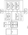
- FIG. 1A illustrates an example memory controller (MC) 114 that may be used to provide selective granularity access and memory protection for memory systems.
- the memory controller 114 determines a selected memory mode based on a memory access request 101.
- the selected memory mode indicates that a memory page is to store a type of error protection information corresponding to the selected memory mode and is to store data for retrieval using an access granularity corresponding to the memory mode.
- the memory controller 114 uses the memory mode logic 103 to store data and the error protection information in the memory page for retrieval using the access granularity.
- FIG. 1B is an example system 100 that may use the memory controller (MC) 114 of FIG. 1A to provide selective granularity access and selective memory protection for memory systems.
- the example system 100 enables selections of different access granularities and different memory error protection schemes for particular applications with particular memory behaviors.
- the example system 100 allows an operating system 134, hardware, an application, a user, or a combination thereof to select a memory mode including a memory error protection scheme and/or an access granularity for a particular application. Selecting a particular memory mode including a particular memory error protection scheme and/or an access granularity for a particular application as disclosed herein increases performance, power efficiency, and/or memory bandwidth utilization while maintaining system reliability.
- the example system 100 includes a multi-core processor 102 that includes multiple processing cores 104 in communication with corresponding caches 106 (e.g., last level caches (LLCs)) via an on-chip network 108.
- the multi-core processor 102 of the illustrated example includes multiple ones of the memory controller 114 of FIG. 1A .
- each of the last level cache banks 106 is in communication with a corresponding memory controller 114.
- the last level cache banks 106 locally cache frequently accessed data in the multi-core processor 102 for retrieval by threads executed by the cores 104.
- a corresponding memory controller 114 accesses memory locations in the memory 112 to accomplish such data reads and/or writes.
- the memory 112 is implemented using error correcting code (ECC) DIMMs (e.g., the DIMMs 110).
- ECC DIMMs 110 have a larger storage capacity than non-ECC DIMMs for storing data memory error protection information (e.g., ECCs) in addition to data.
- Each memory channel 118 associated with corresponding DIMMs 110 provides a 72-bit wide bus including 64-bits for data and 8-bits for memory error protection (e.g., ECCs).
- the memory controllers 114 decode and/or encode ECCs for the ECC DIMMs 110 for read and/or write operations via the memory channels 118 to detect and/or correct errors.
- the memory controllers 114 may implement SECDED, chipkill, SSCDSD, etc. for use with the ECC DIMMs 110.
- the system 100 is configured to select between different memory modes that provide different levels of protection ranging from stronger error protection with a larger access granularity (e.g., more data is accessed during a single memory access operation) to less strong error protection with a smaller access granularity (e.g., less data is accessed during a single memory access operation).
- the system 100 can select between three memory modes for the memory 112 constructed with DRAM devices with different chip widths (e.g., x4, x8, or x16 DRAM devices).
- the memory controllers 114 have ECC logic (e.g., a fine-grained mode logic 204, a medium-grained mode logic 206, and a coarse-grained mode logic of FIG.
- the memory controllers 114 of the illustrated example have access to the multiple memory channels (e.g., each of the memory channels 118) and control each of the memory channels 118 independently and/or simultaneously based on the memory mode to be implemented.
- FIG. 1B shows different access granularities 120, 122, and 124 that may be used in the example system 100 as different memory modes specifying memory access granularities and error protection types.
- a fine-grained mode 120 uses the memory channels 118 independently as separate 64-bit wide logical channels, enabling a 64B memory access 126.
- the fine-grained mode 120 uses chipkill-correct for a x4 DRAM system and SECDED for x8 and x16 DRAM systems.
- a medium-grained mode 122 of the illustrated example uses two memory channels 118 in a lock-step mode to form a 128-bit wide memory channel, enabling a 128B memory access 128.
- the medium-grained mode 122 uses double chipkill for x4 DRAM systems, chipkill for x8 DRAM systems, and DEC for x16 DRAM systems.
- the memory protection in the medium-grained mode 122 is stronger than that provided by the fine-grained mode 120 due to the larger access granularity of the medium-grained mode 122.
- a coarse-grained mode 124 uses four memory channels 118 in a lock-step mode to form a 256-bit wide memory channel, enabling a 256B memory access 130.
- the coarse-grained mode 124 uses quad chipkill for x4 DRAM systems, double chipkill for x8 DRAM systems, and chipkill for x16 DRAM systems.
- the memory protection in the coarse-grained mode 124 is stronger than that provided by the fine-grained mode 120 and the medium-grained mode 122 due to the larger access granularity.
- a corresponding memory controller 114 controls the memory channels 118 independently, and when implementing the medium-grained or coarse-grained memory modes 124, the memory controller 114 controls multiple ones of the memory channels 118 simultaneously.
- the memory channels 118 are provided with respective apparatus 116 to manage memory channels, memory protection, data layout, and/or memory scheduling.
- An example detailed illustration of the apparatus 116 is shown in FIG. 2 .
- the three memory modes 120, 122, and 124 are shown in the illustrated example; however, any other memory mode may additionally or alternatively be implemented in the system 100. For example, larger access granularities with stronger memory protection could be implemented. Furthermore, fewer or more memory modes may be used in the system 100.
- the example system 100 maintains a data layout in the memory 112 that is compatible with the different memory modes to reduce mode switching overhead.
- three memory modes e.g., a 64B fine-grained mode, a 128B medium-grained mode, and a 256B coarse-grained mode
- data is interleaved at the 256B boundary across all of the memory controllers 114, then the 64B data blocks are interleaved across all four 64-bit physical channels within the same memory controller 114.
- the data layout between the memory modes is not changed. If a memory mode is changed between a fine-grained mode and a coarse-grained mode, the data layout remains the same while only the ECC bits are regenerated and replaced.
- the example apparatus 116 of the memory controllers 114 of the illustrated example control the scheduling of memory requests associated with different granularities.
- memory requests include a request to read from a memory page or a request to write to a memory page.
- scheduling memory requests with different granularities creates scheduling challenges when, for example, a coarse-grained request uses multiple memory channels 118 in a lock-step manner to provide a larger access granularity.
- Coarse-grained requests may be scheduled only when multiple memory channels 118 are available at the same time.
- a memory channel 118 may not be available for a coarse-grained request when the memory channel 118 is being used for a fine-grained request.
- the coarse-grained request may be deferred for a relatively long duration when multiple fine-grained requests are received.
- servicing coarse-grained requests only after all fine-grained requests are serviced results in relatively lower system performance than desirable because retrieval of data corresponding to the coarse-grained request may be delayed for a significantly long duration.
- the apparatus 116 enables coarse-grained requests to be serviced in a more timely fashion by prioritizing coarse-grained requests as higher priority when they have been deferred due to fine-grained requests.
- the apparatus 116 of the memory controllers 114 detect a deferment of a coarse-grained request, the priority of the coarse-grained request is raised so that fine-grained requests with a normal priority are not scheduled until the coarse-grained request with the raised priority is serviced.
- the apparatus 116 determines when to increase the priority of a coarse-grained request based on how long the coarse-grained request has been pending without being serviced. For example, the apparatus 116 may increase the priority of a coarse-grained request if the request is not serviced within a threshold period of time (e.g., a timeout). In this manner, coarse-grained requests do not block fine-grained requests from being serviced.
- a threshold period of time e.g., a timeout
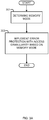
- an example virtual memory manager (VMM) 132 (shown within an operating system (OS) 134) manages memory pages having different access granularities and ECC schemes.
- the virtual memory manager 132 of the illustrated example manages memory mode information for each physical memory page (e.g., memory pages stored in the memory 112) and propagates the memory mode information to the memory controllers 114.
- the virtual memory manager 132 may specify a type of memory mode (e.g., a fine-grained mode or a coarse-grained mode) to be implemented at the memory 112 and a type of ECC (e.g., chipkill, SECDED, etc.) to be implemented at the memory 112 in that particular memory mode.
- a type of memory mode e.g., a fine-grained mode or a coarse-grained mode
- ECC e.g., chipkill, SECDED, etc.
- the virtual memory manager 132 may specify the memory mode to be implemented at the memory mode 112 based on requests from applications and/or based on a determination made by the operating system 134.
- the virtual memory manager 132 enables applications or software to specify particular memory modes to be implemented for particular memory pages stored in the memory 112 (e.g., a request received from an application specifies a particular memory mode).
- a page table entry (PTE) 148 associated with the memory page is augmented by the virtual memory manager 132 to include the particular memory mode.
- PTE page table entry
- the page table entry 148 and the memory mode information is stored in memory 112 and cached in a translation lookaside buffer (TLB) (not shown) to enable applications (e.g., the application 212 of FIG. 2 ) to relatively quickly access the page table entry 148.
- TLB translation lookaside buffer
- memory access requests may be handled using the TLB for memory pages with associated page table entries (e.g., the page table entry 148).
- a TLB miss e.g., requested data is not stored in the TLB
- memory access requests and the mode information are loaded or retrieved from the page tables (e.g., the page table 148) and stored in the TLB.
- the mode information is then propagated to the memory controller 114 to access memory 112.
- the page table entry 148 is propagated through the cache hierarchy (e.g., including the TLB and caches 106) to the memory controllers 114 so that the memory controllers 114 may implement the corresponding ECC logic and access granularity for the memory page stored at the memory 112.
- Selection of memory modes may be done statically (e.g., at the time of compiling the operating system 134 or an application) or dynamically (e.g., during execution of a runtime environment of the operating system 134 and/or an application).
- a programmer or an auto-tuner may specify a particular memory mode and/or provide memory mode information (e.g., a particular ECC and/or a particular access granularity) using annotations, hints, compiler pragmas, and/or default modes.
- a programmer may declare a particular access granularity when memory is allocated based on a memory access pattern.
- a programmer embeds directives into programs to declare the particular memory mode for particular data or memory allocations.
- a compiler generates tags for the particular data and/or memory allocations to denote the particular memory mode.
- the compiler may also generate the tags by analyzing source code of a program associated with the data during compilation.
- the operating system 134 assigns the memory mode to the memory pages with the data based on the tags.
- a programmer may specify stronger memory error protection associated with a large access granularity for use with memory pages storing critical data, and less strong, but more efficient, memory error protection associated with a small access granularity for memory pages storing less-critical data (e.g., temporary data that can be easily reconstructed from another source).
- the virtual memory manager 132 and/or the operating system 134 allocate memory pages using a particular memory mode based on the particular access granularity and/or particular ECC specified by a programmer, an application, and/or the operating system 134.
- the system 100 e.g., the operating system 134 and/or the virtual memory manager 132 selects strong memory error protection for large access granularities and selects less strong, but more efficient, memory error protection for smaller access granularities.
- profilers 146 may collect spatial locality information, memory channel and cache usage data, memory failure rates, row-buffer hit rates, etc. from the caches 106 and memory controllers 114.
- the profilers 146 may be implemented using hardware, software, or a combination of hardware and software.
- profilers 146 are shown outside of the processor 102 in the illustrated example, the profilers 146 may be implemented in the processor 102 or some portions of the profilers 146 may be implemented in the processor 102 and other portions of the profilers 146 may be implemented outside of the processor 102.
- data collected by the profilers 146 is stored in a cache or a cache-like structure.
- the operating system 134 may from time to time evaluate the collected data from the profilers 146 to determine that a different memory mode should be used. For example, the operating system 134 may evaluate the data usage of the application.
- the operating system 134 may determine that a fine-grained memory mode with a 64B cache line may be used. Alternatively, if most of the data usage has high spatial locality (e.g., associated data is stored continuously within a particular 64 byte portion of the memory 112), then a medium-grained memory mode with a 128B cache line may be used or a coarse-grained memory mode with a 256B cache line may be used. In some examples, the operating system 134 also analyzes the memory bandwidth and elects not to use a coarse-grained memory mode where memory bandwidth utilization is high (e.g., availability is low).
- a cache line (e.g., cache line 136a) may include a flag to indicate that the cache line has been accessed since the time that it was stored in cache. For example, a flag may be set to "1" when the cache line has been accessed and the flag may be set to "0" when the cache line has not been accessed.
- the flag information may be sent to the profilers 146 for analysis.
- a profiler 146 may also use an address space identifier (ASID) included for each cache line to analyze spatial locality of a particular application.
- ASID address space identifier
- the operating system 134 evaluates different results (e.g., access granularity during a last time period, memory bandwidth used during the last time period, mode switching overhead, etc.) collected from the profilers 146 and assigns weights to the different results to determine whether a memory mode should be switched and/or what memory mode is to be implemented. For example, mode switching overhead may weigh more heavily in the determination of whether to switch the memory mode than memory bandwidth use.
- the operating system 134 does not analyze results collected from the profilers 146 when the results are associated with data that has been evicted.
- the operating system 134 may reserve a first in, first out (FIFO) in memory 112 so that evicted items may be written to the FIFO.
- the operating system 134 may scan the FIFO region to gather spilled over information in addition to spatial locality information stored in the cache-like structure.
- Switching between different memory modes is useful for applications for which memory pages change patterns and, thus, access granularity preferences, during execution.
- a specific memory page may be unavailable until the switch is complete (e.g., until the ECC is reconstructed according to the newly selected memory mode).
- the operating system 134 may also consider the cost of switching to a different memory mode, because switching the access granularity and ECC in the memory 112 requires ECC reconstruction, which requires a large amount of data to be moved or reorganized.
- the cost of switching to a different memory mode may be relatively low when, for example, the memory system 100 is idle and power consumption is less of a concern.
- switching to a different memory mode may occur during a memory event such as during a page migration or during system checkpointing.
- the operating system 134 may wait for such a memory event (e.g., a page migration or system checkpointing) to occur. If such a memory event does not occur within a threshold period of time (e.g., a time interval or epoch), the switching of the memory mode may be deferred, and a new determination of whether to switch the memory mode may be made based on newly collected data by the profilers 146. Switching the memory mode does not require processor core 104 intervention once the mode switch is started.
- a memory event e.g., a page migration or system checkpointing
- the caches 106 of the illustrated example implement a multi-granularity cache hierarchy to match the different access granularities for accessing the memory 112 based on the selected memory modes. For example, the caches 106 of the illustrated example enable 64B of data to be cached for the fine-grained mode, 128B of data to be cached for the medium-grained mode, and 256B of data to be cached for the coarse-grained mode.
- a detailed view of one of the caches 106 shows cache lines 136 (e.g., 64B of data) associated with corresponding valid and/or dirty bits 138 to indicate if the corresponding cache lines contain valid data or dirty data.
- a cache line 136 may be marked dirty if its data has been changed (e.g., the data is different from the data stored at the memory 112). Setting a dirty bit 138 means that corresponding data is to be written through to the memory 112 (e.g., when the cache line 136 is to be evicted).
- the internal bus width of the caches 106 is provisioned based on the smallest access granularity of the memory modes (e.g., 64B). The width remains the same for different access granularities associated with different memory modes.
- the caches 106 receive 128B-wide data or wider data (e.g., when medium or coarse-grained modes are implemented), the caches 106 allocate two or more cache lines 136 to a same set of cache lines and the co-allocated cache lines 136 are assigned a shared tag.
- cache line 136a, cache line 136b, cache line 136c, and cache line 136d are allocated together and a single tag value (e.g., "1") is shared across all cache lines 136a-136d.
- the assigned tag is stored as tag selection bits 140.
- the cache lines 136a-136d share a tag value, they are combined to form a cache sector.
- the assigned tag is also stored at a tag entry 142.
- a cache line vector 144 acts as a pointer and is associated with the tag entry 142 to point to the corresponding cache lines 136 assigned to the tag entry 142 (e.g., cache lines 136a-136d).
- the cache lines 136 pointed to by the cache line vector 144 are logical sub-cache lines (e.g., 64B of data) within a larger cache line (e.g., 256B of data).
- the cores 104 and/or the memory controllers 114 use the tag selection bits 140 to identify tags 142 of corresponding cache lines 136. Such identification is useful when, for example, a cache line (e.g., a larger cache lines such as 256B) is to be evicted.
- the cache line 136b may have a tag value of "1" at its corresponding tag selection bits 140.
- the tag value "1" is at a corresponding tag entry 142 to identify cache lines 136a, 136c, and 136d via a corresponding cache line vector 144.
- FIG. 2 depicts an example apparatus 116 that may be used in connection with the example memory controllers 114 of FIGS. 1A and 1B and the example system 100 of FIG. 1B to provide selective memory access granularity and selective memory error protection types.
- the example apparatus 116 of the illustrated example is implemented in a memory controller 114 of FIGS. 1A and 1B .
- the example apparatus 116 includes an example mode controller 202, example fine-grained mode logic 204, example medium-grained mode logic 206, example coarse-grained mode logic 208, and an example scheduler 210.
- the example fine-grained mode logic 204, example medium-grained mode logic 206, and example coarse-grained mode logic 208 of the illustrated example correspond to the memory mode logic 103 of FIG. 1A .
- the virtual memory manager 132 ( FIG. 1B ) of the operating system 134 ( FIG. 1B ) of the illustrated example receives operation requests.
- Operation requests include, for example, requests to read data from and/or write data to the cache 106 and/or the memory 112 of FIG. 1 .
- the virtual memory manager 132 receives operation requests from an application 212 and/or the operating system 134.
- operation requests specify a preferred or particular memory mode.
- the memory modes include a fine-grained mode (e.g., the fine-grained mode 120 of FIG. 1B ), a medium-grained mode (e.g., the medium-grained mode 122 of FIG.
- the fine-grained mode provides a smaller access granularity with less strong, but more efficient, ECC protection.
- the medium-grained mode provides a medium access granularity with stronger ECC protection relative to the protection provided by the fine-grained mode.
- the coarse-grained mode provides a larger access granularity with stronger ECC protection relative to the fine and medium-grained modes.
- the application 212 may select the particular memory mode based on the memory mode that will provide an acceptable balance between performance and access granularity and memory error protection.
- the application 212 may select the fine-grained mode because it provides a smaller access granularity, and specifies the selection of the fine-grained mode in the operation request (e.g., a request to write to a memory page). If, for example, the application has high spatial locality, the application 212 selects the coarse-grained mode because it provides a larger access granularity, and specifies the selection of the coarse-grained mode in the operation request.
- the virtual memory manager 132 of the illustrated example communicates the memory mode identified by the application 212 and/or the operating system 134 to the apparatus 116 of the memory controller 114 via the page table entry 148 ( FIG. 1B ).
- the page table entry 148 is augmented to include the particular selected memory mode for a particular memory page to propagate the particular memory mode to the mode controller 202 of the illustrated example so that the mode controller 202 may implement the corresponding ECC logic and access granularity for the memory page.
- the mode controller 202 of the illustrated example implements the particular ECC technique and particular access granularity associated with the memory mode identified in the page table entry 148 at the memory 112 ( FIG. 1B ) using the corresponding fine-grained mode logic 204, the medium-grained mode logic 206, or the coarse-grained mode logic 208. If the operation request received at the virtual memory manager 132 from the application 212 specifies a selection of the fine-grained mode, the mode controller 202 uses the fine-grained mode logic 204 to implement a corresponding ECC and access granularity (e.g., to read and/or write to memory 112 using an error protection type and access granularity corresponding to the fine-grained mode).
- a corresponding ECC and access granularity e.g., to read and/or write to memory 112 using an error protection type and access granularity corresponding to the fine-grained mode.
- the fine-grained mode logic 204 of the illustrated example is provided with logic circuits to use each memory channel as a separate 64-bit wide logical channel to enable a 64B memory access 126 ( FIG. 1B ).
- the fine-grained mode logic 204 of the illustrated example is also provided with logic to implement a chipkill-correct type of error protection for a x4 DRAM system and SECDED type of error protection for x8 and x 16 DRAM systems.
- the mode controller 202 uses the medium-grained mode logic 206 to implement a corresponding ECC and access granularity (e.g., to read and/or write to memory 112 using an error protection type and access granularity corresponding to the medium-grained mode).
- the medium-grained mode logic 206 of the illustrated example is provided with logic to use two memory channels in a lock-step mode to form a 128-bit wide memory channel to enable a 128B memory access.
- the medium-grained mode logic 206 of the illustrated example is also provided with logic to implement a double chipkill type of error protection for x4 DRAM systems, a chipkill type of error protection for x8 DRAM systems, and a DEC type of error protection for x16 DRAM systems.
- the mode controller 202 uses the coarse-grained mode logic 208 to implement a corresponding ECC and access granularity (e.g., to read and/or write to memory 112 using an error protection type and access granularity corresponding to the coarse-grained mode).
- the coarse-grained mode logic 208 of the illustrated example is provided with logic to use four memory channels 118 in a lock-step mode to form a 256-bit wide memory channel to enable a 256B memory access.
- the coarse-grained mode logic 208 of the illustrated example is also provided with logic to implement a quad chipkill type of error protection for x4 DRAM systems, a double chipkill type of error protection for x8 DRAM systems, and a chipkill type of error protection for x16 DRAM systems.
- the example mode controller 202 arranges data in the memory 112 using a data layout in the memory 112 that is compatible with all of the different memory modes to reduce or prevent overhead related to re-organizing the layout of data in the memory 112 each time a different memory mode is selected.
- a data layout in the memory 112 that is compatible with all of the different memory modes to reduce or prevent overhead related to re-organizing the layout of data in the memory 112 each time a different memory mode is selected.
- having three memory modes e.g., a 64B fine-grained mode, a 128B medium-grained mode, and a 256B coarse-grained mode
- data is interleaved at the 256B boundary across all memory controllers, then the 64B data blocks are interleaved across all four 64-bit physical channels corresponding to the same memory controller 114.
- the data layout is not changed when switching between the different memory modes. When the memory mode is changed, the data layout remains the same and the ECC bits are regenerated.
- the scheduler 210 of the illustrated example controls the scheduling of memory requests (e.g., requests to read and/or write to memory 112) having different access granularities.
- the scheduler 210 is configured to arbitrate between the different needs of the different memory modes. For example, data access requests for data stored using a coarse-grained mode (e.g., coarse-grained requests) use multiple memory channels in a lock-step manner to provide a larger access granularity such that none of the memory channels are available for other simultaneous access when the coarse-grained request is being serviced.
- coarse-grained requests are scheduled when multiple memory channels are available at the same time.
- a coarse-grained request is not serviceable if all of the memory channels needed for the access granularity of the coarse-grained mode are not available, for example, due to a memory channel being used to service a fine-grained request. Since a coarse-grained request uses multiple memory channels, the coarse-grained request may be continuously deferred when multiple fine-grained requests are received. In some instances, servicing coarse-grained requests only after all fine-grained requests are serviced degrades system performance. To service coarse-grained requests in a more timely fashion, the scheduler 210 prioritizes coarse-grained requests so that they are not deferred for unduly long durations due to servicing fine-grained requests.
- the scheduler 210 When the scheduler 210 detects that a coarse-grained request has been deferred too long (e.g., its duration of deferment exceeds a threshold), the scheduler 210 increases the priority of the coarse-grained request so that fine-grained requests with a normal priority are not scheduled ahead of the coarse-grained request with the raised priority.
- the mode controller 202 of the illustrated example may also enable switching between different memory modes (e.g., a fine-grained mode may be switched to a coarse-grained mode).
- profilers 146 collect spatial locality information, memory channel and cache usage data, memory failure rates, etc. from the caches 106 and memory controller 114.
- An analyzer 214 of the operating system 134 of the illustrated example evaluates the collected data from the profilers 146 from time to time to determine that a different memory mode should be implemented. For example, the analyzer 214 may evaluate the data usage of the application 212.
- the analyzer 214 may determine that a fine-grained mode with a 64B cache line should be implemented. Alternatively, if most of the data usage has a high spatial locality (e.g., associated data is within contiguous byte portions of the memory 112), then a medium-grained mode with a 128B cache line or a coarse-grained mode may be implemented. The analyzer 214 may also analyze the memory bandwidth usage and/or availability and avoid implementing a coarse-grained mode where memory bandwidth availability is low. In some examples, the analyzer 214 evaluates a variety of results collected from the profilers 146 and assigns weights to the variety of results to determine whether a different memory mode should be selected and/or what memory mode should be selected.
- the analyzer 214 may also analyze the cost of switching between the memory modes because switching the access granularity and ECC used in one or more memory pages in the memory 112 involves re-determining ECCs, which moves a large amount of data within the memory 112.
- the cost of switching between memory modes may be low when, for example, the memory controller 114 is idle and power consumption is less of a concern. Where the memory controller 114 is not idle and/or power consumption is more of a concern, switching between memory modes may occur during a memory event such as a page migration or a system checkpointing event.
- the analyzer 214 may wait for such a memory event to occur. If such a memory event does not occur within a threshold period of time, the switching of the memory mode may be deferred, and a new determination of whether to switch the memory mode may be made based on newly collected data by the profilers 146. To switch the memory mode, the virtual memory manager 132 may propagate the new memory mode to the mode controller 202 by updating the page table entry 148.
- the mode controller 202 uses the ECC technique and access granularity for the new memory mode using the fine-grained mode logic 204, the medium-grained mode logic 206, and/or the coarse-grained mode logic 208 and implements the corresponding ECC technique and the corresponding access granularity at the memory 112.
- the cache 106 of the illustrated example provides a multi-granularity cache hierarchy to implement memory modes specified or selected by the application 212.
- the cache 106 of the illustrated example enables a 64B cache line size for the fine-grained mode, a 128B cache line size for the medium-grained mode, and a 256B cache line size for the coarse-grained mode.
- the cache 106 receives 128B or wider of data and allocates two or more cache lines to a same set of associated cache lines.
- the cache 106 assigns a same tag (e.g., a tag 142) to all of the associated cache lines (e.g., two or more cache lines 136).
- the assigned tag 142 is stored at the cache 106, and a cache line vector 144 is associated with the assigned tag 142 to point to the cache lines 136 to which the tag 142 is assigned.
- the cache lines 136 pointed to by the cache line vector 144 are logical sub-cache lines (e.g., 64B of data) within a larger cache line (e.g., 256B of data).
- tag selection bits 140 are indicative of a tag 142 assigned to a cache line 136 or a set of associated cache lines 136. Such identifications provided by tag selection bits 140 are useful when, for example, a cache line (e.g., a larger cache line such as a 256B cache line) is to be evicted.
- the example apparatus 116 of FIG. 2 enable switching between different memory access granularities and different types of error protection techniques in a memory system. Selecting different memory error protection techniques (e.g., ECC techniques) and memory access granularities based on application behaviors and/or system memory utilization increases system performance, power efficiency, energy efficiency, and reliability.
- ECC techniques e.g., ECC techniques
- the example mode controller 202, the example fine-grained mode logic 204, the example medium-grained mode logic 206, the example coarse-grained logic 208, the example scheduler 210, and/or, more generally, the example apparatus 116 of FIG. 2 may be implemented by hardware, software, firmware and/or any combination of hardware, software and/or firmware.
- any of the example mode controller 202, the example fine-grained mode logic 204, the example medium-grained mode logic 206, the example coarse-grained logic 208, the example scheduler 210, and/or, more generally, the example apparatus 116 could be implemented by one or more circuit(s), programmable processor(s), application specific integrated circuit(s) (ASIC(s)), programmable logic device(s) (PLD(s)) and/or field programmable logic device(s) (FPLD(s)), etc.
- ASIC application specific integrated circuit
- PLD programmable logic device
- FPLD field programmable logic device
- At least one of the example mode controller 202, the example fine-grained mode logic 204, the example medium-grained mode logic 206, the example coarse-grained logic 208, and/or the example scheduler 210 is hereby expressly defined to include a tangible computer-readable storage medium such as a memory, DVD, CD, etc. storing the software and/or firmware.
- the example apparatus 116 illustrated in FIG. 2 may include one or more elements, processes and/or devices in addition to, or instead of, those illustrated in FIG. 2 , and/or may include more than one of any or all of the illustrated elements, processes and devices.
- FIGS. 3A , 3B , and 4 Flowcharts representative of example machine-readable instructions for implementing the example apparatus 116 of FIG. 2 are shown in FIGS. 3A , 3B , and 4 .
- the machine-readable instructions comprise one or more programs for execution by one or more processors similar or identical to the processor 102 of FIG. 1B .
- the program(s) may be embodied in software stored on a tangible computer-readable storage medium such as a memory associated with the processor 102, but the entire program(s) and/or parts thereof could alternatively be executed by one or more devices other than the processor 102 and/or embodied in firmware or dedicated hardware.
- the example program(s) is/are described with reference to the flowcharts illustrated in FIGS.
- FIGS. 3A , 3B , and/or 4 may be implemented using coded instructions (e.g., computer-readable instructions) stored on a tangible computer-readable storage medium (e.g., a storage device or storage disk) such as a hard disk drive, a flash memory, a read-only memory (“ROM”), a cache, a random-access memory (“RAM”) and/or any other physical storage in which information is stored for any duration (e.g., for extended time periods, permanently, brief instances, for temporarily buffering, and/or for caching of the information).
- a tangible computer-readable storage medium e.g., a storage device or storage disk
- a storage device or storage disk such as a hard disk drive, a flash memory, a read-only memory (“ROM”), a cache, a random-access memory (“RAM”) and/or any other physical storage in which information is stored for any duration (e.g., for extended time periods, permanently, brief instances, for temporarily buffering, and/or for caching of the information).
- FIGS. 3A , 3B , and/or 4 may be implemented using coded instructions (e.g., computer-readable instructions) stored on a non-transitory computer-readable medium (e.g., a storage device or storage disk) such as a hard disk drive, a flash memory, a read-only memory, a cache, a random-access memory and/or any other storage media in which information is stored for any duration (e.g., for extended time periods, permanently, brief instances, for temporarily buffering, and/or for caching of the information).
- a non-transitory computer-readable medium e.g., a storage device or storage disk
- a non-transitory computer-readable medium such as a hard disk drive, a flash memory, a read-only memory, a cache, a random-access memory and/or any other storage media in which information is stored for any duration (e.g., for extended time periods, permanently, brief instances, for temporarily buffering, and/or for caching of the information).
- FIG. 3A is a flow diagram representative of example machine-readable instructions that can be executed to implement the example memory controller 114 of FIG. 2 to determine and implement a selected memory mode.
- the memory controller 114 ( FIG. 2 ) determines a selected memory mode to be used based on a request to access data in memory (block 301).
- the memory mode indicates that a memory page is to store a corresponding type of error protection information and is to be accessed using a corresponding memory access granularity.
- the memory controller 114 implements the error protection with the corresponding access granularity based on the memory mode (block 303) determined at block 301. For example, the memory controller 114 writes the corresponding type of error protection information (e.g., corresponding ECCs) and data to the memory page using a channel data width corresponding to the corresponding access granularity.
- corresponding type of error protection information e.g., corresponding ECCs
- FIG. 3B is a flow diagram representative of machine-readable instructions to access memory using different memory modes.
- the virtual memory manager 132 receives an operation request (block 302).
- an operation request is a request to read data from and/or write data to the cache 106 ( FIG. 2 ) and/or the memory 112 ( FIG. 2 ).
- Operation requests include information specifying a particular memory mode such as a fine-grained mode, a medium-grained mode, or a coarse-grained mode.
- the application 212 selects the particular memory mode that provides a desirable performance based on access granularity and memory error protection.
- the virtual memory manager 132 identifies the memory mode based on the memory operation request received from the application 212 (block 304) and communicates the memory mode to the mode controller 202 ( FIG. 2 ) by updating the page table entry 148 ( FIG. 2 ). If the operation request received from the application 212 specifies the fine-grained mode, the mode controller 202 is to implement the fine-grained mode logic 204 to generate the ECC information and to configure the access granularity to be used for the requested memory access.
- the fine-grained mode logic 204 of the illustrated example configures each of the memory channels 118 ( FIG. 1B ) as a 64-bit wide logical channel to enable a 64B memory access 126 ( FIG. 1B ).
- the fine-grained mode logic 204 of the illustrated example also implements logic to implement a chipkill-correct type of error protection for a x4 DRAM system and an SECDED type of error protection for x8 and x 16 DRAM systems. If the operation request received from the application 212 specifies the medium-grained mode, the mode controller 202 is to implement the medium-grained mode logic 206 to generate the ECC information and to configure the access granularity to be used for the requested memory access. The medium-grained mode logic 206 of the illustrated example configures two of the memory channels 18 to operate in a lock-step mode to construct a 128-bit wide memory channel to enable a 128B memory access 128 ( FIG. 1B ).
- the medium-grained mode logic 206 of the illustrated example also implements a double chipkill type of error protection for x4 DRAM systems, a chipkill type of error protection for x8 DRAM systems, and/or a DEC type of error protection for x16 DRAM systems.
- the mode controller 202 is to implement the coarse-grained mode logic 208 to generate the error protection information (e.g., ECC) and to configure the access granularity to be used for the requested memory access.
- the coarse-grained mode logic 208 of the illustrated example configures four of the memory channels 118 to operate in a lock-step mode to construct a 256-bit wide memory channel to enable a 256B memory access 130 ( FIG.
- the coarse-grained mode logic 208 of the illustrated example also implements a quad chipkill type of error protection for x4 DRAM systems, a double chipkill type of error protection for x8 DRAM systems, and/or a chipkill type of error protection for x16 DRAM systems.
- the scheduler 210 determines if the memory mode specified in the operation request is a fine-grained mode (block 306). If the specified memory mode is not a fine-grained mode (block 306), the scheduler 210 determines if a sufficient number of memory channels are available (block 308) to operate in a lock-step manner to implement a medium-grained mode or a coarse-grained mode. For example, a coarse-grained request may require four memory channels to operate in a lock-step manner and such memory channels may not be available when another memory operation is being implemented (e.g., a fine-grained request requiring a single memory channel).
- the mode controller 202 services the requested memory operation (block 310) using the selected error protection technique and access granularity.
- the scheduler 210 increases the priority for the requested memory operation based on a scheduling policy (block 312).
- a scheduling policy may specify a duration of pendency threshold related to an amount of time for which requests are pending. For example, the scheduler 210 may increase the priority for the requested memory operation if the requested memory operation is not serviced within a threshold period of time (e.g., a timeout) defined by a scheduling policy.
- durations of pendency for scheduling policies may be predetermined based on, for example, performance criteria, bandwidth criteria, power-consumption criteria, and/or any other suitable criteria.
- the increased priority of the request is used to cause the scheduler 210 to defer servicing fine-grained requests until the medium-grained or coarse-grained request is serviced, and to schedule the requested operation as soon as there are sufficient channels available to service the requested operation.
- control then returns to block 302.
- the scheduler 210 also continues to monitor the high-priority request (shown in FIG. 3B by a dashed line) until sufficient memory channels are available to service the high-priority request.
- the scheduler 210 determines if there is a high-priority request pending (block 314).
- a high-priority request may be pending if a medium or coarse-grained request was unable to be serviced due to the unavailability of a sufficient number of memory channels to operate in lock-step mode. If a high-priority request is pending (block 314), the mode controller 202 determines if a sufficient number of memory channels are available to execute the pending high-priority request (block 316).
- the current request is put on hold (block 318) and control returns to block 316 to allow memory channels to become available to service the pending high-priority request.
- the mode controller 202 executes the pending high-priority request (block 320) using the corresponding error protection technique and access granularity.
- the current operation request (e.g., a fine-grained request) is then serviced (block 310) by the mode controller 202 according to the corresponding error protection technique and access granularity.
- the mode controller 202 services the current operation request using the corresponding error protection technique and access granularity (block 310). After the pending priority request is serviced (block 320) and/or the current request is serviced (block 310), control returns to block 302.
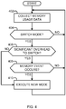
- FIG. 4 is a flow diagram representative of example machine-readable instructions that can be executed to implement the example system 200 of FIG. 2 to switch between different memory modes.
- Profilers 146 FIG. 2
- the analyzer 214 of the operating system 134 FIG. 2
- the analyzer 214 periodically evaluates the collected data from the profilers 146 to determine if a different memory mode should be implemented (block 404). In determining whether to switch the memory mode, the analyzer 214 evaluates the data usage of the application 212 ( FIG. 2 ).
- the analyzer 214 determines that a fine-grained mode with a 64B cache line is to be implemented. Alternatively, if most of the data usage has a high spatial locality (e.g., associated data is stored in contiguous 64 byte portions of the memory 112), a medium-grained mode with a 128B cache line or a coarse-grained mode with a 256B cache line is to be implemented. In some examples, the analyzer 214 also considers the memory bandwidth, and avoids implementing a coarse-grained mode where memory bandwidth (e.g., availability) is low. In some examples, the analyzer 214 evaluates a variety of results collected from the profilers 146 and assigns weights to the variety of results to determine whether to switch memory modes and/or what memory mode is to be implemented.
- the analyzer 214 determines that the memory mode should not be switched (block 404)
- control returns to block 402, at which the profilers 146 continue to collect memory usage data.
- the analyzer 214 determines if there is significant overhead (e.g., cost) to switch the memory mode. Switching a memory mode may be costly because switching the access granularity and the error protection information in the memory 112 ( FIG. 2 ) requires redetermining ECCs or other error protection codes, which requires a large amount of data to be accessed. The cost of switching the memory mode may be low when, for example, the memory controller 114 is idle and power consumption is less of a concern.
- the analyzer 214 determines if a memory event (e.g., a page migration or a system checkpointing event) is to occur (block 408). Switching between memory modes may occur during a memory event as reading and/or writing of data in the memory 112 occurs during such events and, thus, switching the memory mode during these events incurs less overhead for reconstructing the ECC. If a memory event is to occur within a threshold time period (block 408), to execute the new memory mode, the virtual memory manager 132 ( FIG. 2 ) communicates the new memory mode to the mode controller 202 using the page table entry 148 ( FIG.
- a memory event e.g., a page migration or a system checkpointing event
- control returns to block 402 and the determination of whether to switch the memory mode is made based on newly collected data. If the analyzer 214 determines that there is not a significant overhead to switch the memory mode (block 406), the virtual memory manager 132 communicates the new memory mode to the mode controller 202 using the page table entry 148 and the mode controller 202 implements the new memory mode by servicing memory requests using a corresponding error protection technique and access granularity (block 410). Control then returns to block 402.
Claims (13)
- Einrichtung zum Bereitstellen eines selektiven Speicherfehlerschutzes und einer Speicherzugriffsgranularität, Folgendes umfassend:
einen Speicher-Controller (114) zum:Bestimmen eines ersten Speichermodus auf Grundlage einer ersten Anfrage (101) zum Zugreifen auf Daten in einem Speicher (112), wobei der erste Speichermodus eine erste Speicherschutztechnik und eine erste Speicherzugriffsgranularität angibt, die zum Speichern von Daten auf einer ersten Speicherseite zum Abrufen unter Verwendung der ersten Speicherzugriffsgranularität zu verwenden sind;Speichern der Daten und einer ersten Art von Fehlerschutzinformationen, die der ersten Speicherschutztechnik auf der ersten Speicherseite zum Abrufen unter Verwendung der Zugriffsgranularität entsprechen; und dadurch gekennzeichnet ist, dass der Speicher-Controller (114) ferner für Folgendes vorliegt:Identifizieren eines zweiten Speichermodus auf Grundlage einer zweiten Anfrage zum Zugreifen auf Daten in einem Speicher, wobei der zweite Speichermodus eine zweite Speicherschutztechnik und eine zweite Speicherzugriffsgranularität angibt, die zu verwenden sind, um Daten auf einer zweiten Speicherseite zu speichern;Speichern von Daten und einer zweiten Art von Fehlerschutzinformationen, die der zweiten Speicherschutztechnik zum Abrufen unter Verwendung der zweiten Zugriffsgranularität entsprechen; undwobei die zweite Art von Fehlerschutzinformationen eine stärkere Fehlerstabilität bereitstellt als die erste Art von Fehlerschutzinformationen und die zweite Zugriffsgranularität einem breiteren Datenkanal entspricht, als die erste Zugriffsgranularität. - Einrichtung nach Anspruch 1, wobei die Anfrage (101) eine Anfrage zum Lesen von der Speicherseite und/oder eine Anfrage zum Schreiben auf die Speicherseite ist, wobei die Anfrage von einer Anwendung (212) empfangen wird.
- Einrichtung nach Anspruch 1, wobei der Speicher-Controller (114) mehrere Speicherkanäle konfiguriert, um in Lockstep betrieben zu werden, um die zweite Zugriffsgranularität zu implementieren.
- Einrichtung nach Anspruch 1, wobei der Speichermodus auf Grundlage von Betriebsbedingungen des Speicher-Controllers (114) ausgewählt wird.
- System zum Bereitstellen eines selektiven Speicherfehlerschutzes und einer Speicherzugriffsgranularität, umfassend die Einrichtung nach einem der Ansprüche 1 bis 4, wobei das System ferner Folgendes umfasst:einen Speicherverwalter, um den ersten Speichermodus in der ersten Anfrage von einem Betriebssystem oder einer Anwendung (212), die auf dem Betriebssystem ausgeführt wird, zu empfangen; undeinen Cache (106) einschließlich mehrerer Cacheleitungen, um Abschnitte der Daten der ersten Speicherseite auf Grundlage der ersten Speicherzugriffsgranularität zu speichern.
- System nach Anspruch 5, wobei der Cache (106) dazu dient, den mehreren Cacheleitungen, die die Abschnitte der Daten speichern, einen Tag zuzuordnen.
- System nach Anspruch 6, wobei der Tag mit einem Vektor verknüpft ist, um zu den mehreren Cacheleitungen, die die Abschnitte der Daten speichern, zu zeigen.
- System nach Anspruch 5, wobei die mehreren Cacheleitungen kombiniert sind, um einen Cachesektor auszubilden.
- System nach Anspruch 5, wobei der Speicher-Controller (114) dazu dient, die Fehlerschutzinformationen zu erzeugen, die dem Speichermodus entsprechen.
- System nach Anspruch 5, wobei die Anfrage (101) eine Anfrage zum Zuteilen einer Speicherseite, eine Anfrage zum Lesen von der Speicherseite und/oder eine Anfrage zum Schreiben auf die Speicherseite ist.
- Verfahren zum Bereitstellen eines selektiven Speicherfehlerschutzes und einer Speicherzugriffsgranularität, Folgendes umfassend:Bestimmen (301) eines ersten Speichermodus auf Grundlage einer ersten Anfrage (101) zum Zugreifen auf Daten in einem Speicher (112), wobei der erste Speichermodus eine erste Speicherschutztechnik und eine erste Speicherzugriffsgranularität angibt, die zum Speichern von Daten auf einer ersten Speicherseite zum Abrufen unter Verwendung der ersten Speicherzugriffsgranularität zu verwenden sind;Schreiben einer ersten Art von Fehlerschutzinformationen, die der ersten Speicherschutztechnik entsprechen, und von Daten an die erste Speicherseite, unter Verwendung einer ersten Kanaldatenbreite, die der ersten Speicherzugriffsgranularität entspricht; und gekennzeichnet durch:Bestimmen eines zweiten Speichermodus auf Grundlage einer zweiten Anfrage zum Zugreifen auf Daten in dem Speicher, wobei der zweite Speichermodus eine zweite Speicherschutztechnik und eine zweite Speicherzugriffsgranularität angibt, die zu verwenden sind, um Daten auf einer zweiten Speicherseite zum Abrufen unter Verwendung der zweiten Speicherzugriffsgranularität zu speichern; undSchreiben einer zweiten Art von Fehlerschutzinformationen, die der zweiten Speicherschutztechnik entsprechen, und von Daten an die zweite Speicherseite unter Verwendung einer zweiten Kanaldatenbreite, die der zweiten Speicherzugriffsgranularität entspricht; undwobei die zweite Art von Fehlerschutzinformationen eine stärkere Fehlerstabilität bereitstellt als die erste Art von Fehlerschutzinformationen und die zweite Kanaldatenbreite einem breiteren Datenkanal entspricht, als die erste Kanaldatenbreite.
- Verfahren nach Anspruch 11, wobei der Speichermodus durch ein Betriebssystem oder eine Anwendung (212), die auf dem Betriebssystem ausgeführt wird, ausgewählt wird.
- Verfahren nach Anspruch 11, wobei die Fehlerschutzinformationen ein Fehlerkorrekturcode sind; und wobei die zweite Kanaldatenbreite zweimal die Kanaldatenbreite ist.
Applications Claiming Priority (1)
| Application Number | Priority Date | Filing Date | Title |
|---|---|---|---|
| PCT/US2012/063421 WO2014070200A1 (en) | 2012-11-02 | 2012-11-02 | Selective error correcting code and memory access granularity switching |
Publications (3)
| Publication Number | Publication Date |
|---|---|
| EP2915045A1 EP2915045A1 (de) | 2015-09-09 |
| EP2915045A4 EP2915045A4 (de) | 2017-06-14 |
| EP2915045B1 true EP2915045B1 (de) | 2019-01-02 |
Family
ID=50627886
Family Applications (1)
| Application Number | Title | Priority Date | Filing Date |
|---|---|---|---|
| EP12887804.8A Active EP2915045B1 (de) | 2012-11-02 | 2012-11-02 | Selektiver fehlerkorrekturcode und speicherzugangsgranularitätswechsel |
Country Status (5)
| Country | Link |
|---|---|
| US (1) | US10318365B2 (de) |
| EP (1) | EP2915045B1 (de) |
| CN (1) | CN104903864B (de) |
| TW (1) | TWI514406B (de) |
| WO (1) | WO2014070200A1 (de) |
Families Citing this family (22)
| Publication number | Priority date | Publication date | Assignee | Title |
|---|---|---|---|---|
| KR20150132099A (ko) | 2013-03-20 | 2015-11-25 | 휴렛-팩커드 디벨롭먼트 컴퍼니, 엘.피. | 서로 다른 계층 레벨의 메모리 노드를 가진 메모리 시스템에서의 데이터 캐싱 |
| US9537745B1 (en) * | 2014-03-07 | 2017-01-03 | Google Inc. | Distributed virtual machine disk image deployment |
| US9697094B2 (en) | 2015-02-06 | 2017-07-04 | Intel Corporation | Dynamically changing lockstep configuration |
| US10410738B2 (en) * | 2016-03-15 | 2019-09-10 | Toshiba Memory Corporation | Memory system and control method |
| CN107239224B (zh) * | 2016-03-29 | 2020-05-12 | 群联电子股份有限公司 | 数据保护方法、存储器控制电路单元与存储器存储装置 |
| US10169126B2 (en) * | 2016-10-12 | 2019-01-01 | Samsung Electronics Co., Ltd. | Memory module, memory controller and systems responsive to memory chip read fail information and related methods of operation |
| US10606690B2 (en) * | 2017-09-29 | 2020-03-31 | Intel Corporation | Memory controller error checking process using internal memory device codes |
| US10346346B1 (en) | 2017-12-21 | 2019-07-09 | Xilinx, Inc. | Inline ECC function for system-on-chip |
| US11086526B2 (en) * | 2018-06-07 | 2021-08-10 | Micron Technology, Inc. | Adaptive line width cache systems and methods |
| US10649922B2 (en) * | 2018-08-06 | 2020-05-12 | Apple Inc. | Systems and methods for scheduling different types of memory requests with varying data sizes |
| US11360544B2 (en) * | 2018-10-03 | 2022-06-14 | Google Llc | Power management systems and methods for a wearable computing device |
| US11010057B2 (en) | 2019-05-29 | 2021-05-18 | Western Digital Technologies, Inc. | Storage system and method for storage system calibration |
| US10997081B2 (en) | 2019-05-29 | 2021-05-04 | Western Digital Technologies, Inc. | Host and method for storage system calibration |
| CN110442345B (zh) * | 2019-06-21 | 2021-01-29 | 华为技术有限公司 | 一种编译方法、运行方法及设备 |
| KR20210012641A (ko) * | 2019-07-26 | 2021-02-03 | 에스케이하이닉스 주식회사 | 메모리 시스템, 데이터 시스템 및 그 동작방법 |
| CN110729018B (zh) * | 2019-09-06 | 2021-06-01 | 天津大学 | 基于识别动态故障模式的存储器诊断数据压缩方法 |
| US11656995B2 (en) * | 2019-11-26 | 2023-05-23 | Micron Technology, Inc. | Dynamic access granularity in a cache media |
| KR20210147131A (ko) | 2020-05-27 | 2021-12-07 | 삼성전자주식회사 | 반도체 메모리 모듈을 액세스하는 방법 |
| KR20210147132A (ko) | 2020-05-27 | 2021-12-07 | 삼성전자주식회사 | 메모리 장치 및 메모리 장치를 포함하는 메모리 모듈 |
| US20210151120A1 (en) * | 2020-12-24 | 2021-05-20 | Intel Corporation | Modular error correction code circuitry |
| US11934270B2 (en) * | 2022-06-02 | 2024-03-19 | Micron Technology, Inc. | Write command execution for data protection and recovery schemes |
| CN115168087B (zh) * | 2022-07-08 | 2024-03-19 | 超聚变数字技术有限公司 | 一种确定内存故障的修复资源粒度的方法及装置 |
Family Cites Families (23)
| Publication number | Priority date | Publication date | Assignee | Title |
|---|---|---|---|---|
| US6938133B2 (en) * | 2001-09-28 | 2005-08-30 | Hewlett-Packard Development Company, L.P. | Memory latency and bandwidth optimizations |
| US7143264B2 (en) * | 2002-10-10 | 2006-11-28 | Intel Corporation | Apparatus and method for performing data access in accordance with memory access patterns |
| US8032688B2 (en) * | 2005-06-30 | 2011-10-04 | Intel Corporation | Micro-tile memory interfaces |
| US20070260841A1 (en) * | 2006-05-02 | 2007-11-08 | Hampel Craig E | Memory module with reduced access granularity |
| US7539842B2 (en) * | 2006-08-15 | 2009-05-26 | International Business Machines Corporation | Computer memory system for selecting memory buses according to physical memory organization information stored in virtual address translation tables |
| US8321637B2 (en) | 2007-05-14 | 2012-11-27 | International Business Machines Corporation | Computing system with optimized support for transactional memory |
| US20100005218A1 (en) * | 2008-07-01 | 2010-01-07 | International Business Machines Corporation | Enhanced cascade interconnected memory system |
| US8266498B2 (en) | 2009-03-31 | 2012-09-11 | Freescale Semiconductor, Inc. | Implementation of multiple error detection schemes for a cache |
| KR101575248B1 (ko) * | 2009-04-30 | 2015-12-07 | 삼성전자주식회사 | 메모리 컨트롤러 및 그것을 포함하는 메모리 시스템 |
| US8190974B2 (en) * | 2009-09-28 | 2012-05-29 | Nvidia Corporation | Error detection and correction for external DRAM |
| US8650446B2 (en) | 2010-03-24 | 2014-02-11 | Apple Inc. | Management of a non-volatile memory based on test quality |
| KR101662827B1 (ko) * | 2010-07-02 | 2016-10-06 | 삼성전자주식회사 | 쓰기 패턴에 따라 데이터 블록의 쓰기 모드를 선택하는 메모리 시스템 및 그것의 데이터 쓰기 방법 |
| EP2418648B1 (de) * | 2010-07-29 | 2013-03-06 | STMicroelectronics (Grenoble 2) SAS | RAM-Speichergerät, das selektiv mit ECC geschützt werden kann |
| US8990660B2 (en) | 2010-09-13 | 2015-03-24 | Freescale Semiconductor, Inc. | Data processing system having end-to-end error correction and method therefor |
| CN103329103B (zh) | 2010-10-27 | 2017-04-05 | 希捷科技有限公司 | 使用用于基于闪存的数据存储的自适应ecc技术的方法和设备 |
| KR20120082218A (ko) * | 2011-01-13 | 2012-07-23 | (주)인디링스 | 파티션 정보를 기초로 호스트의 요청에 대한 처리 기법을 적응적으로 결정하는 스토리지 장치 및 상기 스토리지 장치의 동작 방법 |
| JP5605238B2 (ja) | 2011-01-25 | 2014-10-15 | ソニー株式会社 | メモリシステムおよびその動作方法 |
| US9615326B2 (en) * | 2011-06-30 | 2017-04-04 | Intel Corporation | System and method of improving power efficiency in wireless communication system |
| US9268719B2 (en) * | 2011-08-05 | 2016-02-23 | Rambus Inc. | Memory signal buffers and modules supporting variable access granularity |
| BR112014013390A2 (pt) * | 2011-12-20 | 2017-06-13 | Intel Corp | redução de potência parcial dinâmica de cache de lado de memória em hierarquia de memória de 2 níveis |
| CN102609378B (zh) * | 2012-01-18 | 2016-03-30 | 中国科学院计算技术研究所 | 一种消息式内存访问装置及其访问方法 |
| US9600359B2 (en) * | 2012-05-31 | 2017-03-21 | Hewlett Packard Enterprise Development Lp | Local error detection and global error correction |
| US20140047452A1 (en) * | 2012-08-08 | 2014-02-13 | Battelle Memorial Institute | Methods and Systems for Scalable Computing on Commodity Hardware for Irregular Applications |
-
2012
- 2012-11-02 EP EP12887804.8A patent/EP2915045B1/de active Active
- 2012-11-02 US US14/437,684 patent/US10318365B2/en active Active
- 2012-11-02 CN CN201280078087.3A patent/CN104903864B/zh active Active
- 2012-11-02 WO PCT/US2012/063421 patent/WO2014070200A1/en active Application Filing
-
2013
- 2013-10-16 TW TW102137300A patent/TWI514406B/zh active
Non-Patent Citations (1)
| Title |
|---|
| None * |
Also Published As
| Publication number | Publication date |
|---|---|
| TWI514406B (zh) | 2015-12-21 |
| WO2014070200A1 (en) | 2014-05-08 |
| US10318365B2 (en) | 2019-06-11 |
| US20150278004A1 (en) | 2015-10-01 |
| EP2915045A4 (de) | 2017-06-14 |
| EP2915045A1 (de) | 2015-09-09 |
| CN104903864B (zh) | 2018-09-04 |
| CN104903864A (zh) | 2015-09-09 |
| TW201432704A (zh) | 2014-08-16 |
Similar Documents
| Publication | Publication Date | Title |
|---|---|---|
| EP2915045B1 (de) | Selektiver fehlerkorrekturcode und speicherzugangsgranularitätswechsel | |
| RU2666241C2 (ru) | Перераспределение сегментов памяти для решения проблемы фрагментации | |
| US9575889B2 (en) | Memory server | |
| KR101449524B1 (ko) | 스토리지 장치 및 컴퓨팅 시스템 | |
| US7802057B2 (en) | Priority aware selective cache allocation | |
| Lin et al. | SECRET: Selective error correction for refresh energy reduction in DRAMs | |
| WO2018174982A1 (en) | Dynamic memory remapping to reduce row-buffer conflicts | |
| KR101581859B1 (ko) | 메모리 시스템 및 그것의 플래시 변환 계층의 데이터 관리 방법 | |
| CN106469126B (zh) | 处理io请求的方法及其存储控制器 | |
| US8645612B2 (en) | Information processing device and information processing method | |
| US9355035B2 (en) | Dynamic write priority based on virtual write queue high water mark for set associative cache using cache cleaner when modified sets exceed threshold | |
| US20150248316A1 (en) | System and method for dynamically selecting between memory error detection and error correction | |
| US20210056030A1 (en) | Multi-level system memory with near memory capable of storing compressed cache lines | |
| WO2020176523A1 (en) | Double threshold controlled scheduling of memory access commands | |
| CN114902198A (zh) | 用于异构存储器系统的信令 | |
| Luo et al. | Using ECC DRAM to adaptively increase memory capacity | |
| CN111459400B (zh) | 在存储服务器中进行基于管线的存取管理的方法及设备 | |
| US11175859B1 (en) | Managing memory commands in a memory subsystem by adjusting a maximum number of low priority commands in a DRAM controller | |
| EP4120087B1 (de) | Systeme, verfahren und vorrichtungen für nutzungsbewusste speicherzuweisung | |
| US20240061589A1 (en) | Code rate as function of logical saturation | |
| Xu et al. | Asymmetric Redundancy: An Enhanced Redundancy Strategy for MLC NAND Flash Memory Storage Systems | |
| US8719502B2 (en) | Adaptive self-repairing cache |
Legal Events
| Date | Code | Title | Description |
|---|---|---|---|
| PUAI | Public reference made under article 153(3) epc to a published international application that has entered the european phase |
Free format text: ORIGINAL CODE: 0009012 |
|
| 17P | Request for examination filed |
Effective date: 20150423 |
|
| AK | Designated contracting states |
Kind code of ref document: A1 Designated state(s): AL AT BE BG CH CY CZ DE DK EE ES FI FR GB GR HR HU IE IS IT LI LT LU LV MC MK MT NL NO PL PT RO RS SE SI SK SM TR |
|
| AX | Request for extension of the european patent |
Extension state: BA ME |
|
| DAX | Request for extension of the european patent (deleted) | ||
| RAP1 | Party data changed (applicant data changed or rights of an application transferred) |
Owner name: HEWLETT PACKARD ENTERPRISE DEVELOPMENT L.P. |
|
| RIC1 | Information provided on ipc code assigned before grant |
Ipc: G06F 11/07 20060101ALI20170120BHEP Ipc: G11C 29/02 20060101AFI20170120BHEP Ipc: G11C 7/20 20060101ALI20170120BHEP Ipc: G06F 11/10 20060101ALI20170120BHEP Ipc: G06F 12/0875 20160101ALI20170120BHEP Ipc: G11C 29/42 20060101ALI20170120BHEP Ipc: G11C 29/52 20060101ALI20170120BHEP |
|
| REG | Reference to a national code |
Ref country code: DE Ref legal event code: R079 Ref document number: 602012055576 Country of ref document: DE Free format text: PREVIOUS MAIN CLASS: G06F0011080000 Ipc: G11C0029020000 |
|
| RA4 | Supplementary search report drawn up and despatched (corrected) |
Effective date: 20170512 |
|
| RIC1 | Information provided on ipc code assigned before grant |
Ipc: G11C 29/42 20060101ALI20170508BHEP Ipc: G06F 11/07 20060101ALI20170508BHEP Ipc: G06F 11/10 20060101ALI20170508BHEP Ipc: G11C 29/52 20060101ALI20170508BHEP Ipc: G06F 12/0875 20160101ALI20170508BHEP Ipc: G11C 29/02 20060101AFI20170508BHEP Ipc: G11C 7/20 20060101ALI20170508BHEP |
|
| GRAP | Despatch of communication of intention to grant a patent |
Free format text: ORIGINAL CODE: EPIDOSNIGR1 |
|
| STAA | Information on the status of an ep patent application or granted ep patent |
Free format text: STATUS: GRANT OF PATENT IS INTENDED |
|
| INTG | Intention to grant announced |
Effective date: 20180719 |
|
| GRAS | Grant fee paid |
Free format text: ORIGINAL CODE: EPIDOSNIGR3 |
|
| GRAA | (expected) grant |
Free format text: ORIGINAL CODE: 0009210 |
|
| STAA | Information on the status of an ep patent application or granted ep patent |
Free format text: STATUS: THE PATENT HAS BEEN GRANTED |
|
| AK | Designated contracting states |
Kind code of ref document: B1 Designated state(s): AL AT BE BG CH CY CZ DE DK EE ES FI FR GB GR HR HU IE IS IT LI LT LU LV MC MK MT NL NO PL PT RO RS SE SI SK SM TR |
|
| REG | Reference to a national code |
Ref country code: GB Ref legal event code: FG4D |
|
| REG | Reference to a national code |
Ref country code: CH Ref legal event code: EP Ref country code: AT Ref legal event code: REF Ref document number: 1085402 Country of ref document: AT Kind code of ref document: T Effective date: 20190115 |
|
| REG | Reference to a national code |
Ref country code: IE Ref legal event code: FG4D |
|
| REG | Reference to a national code |
Ref country code: DE Ref legal event code: R096 Ref document number: 602012055576 Country of ref document: DE |
|
| REG | Reference to a national code |
Ref country code: NL Ref legal event code: FP |
|
| REG | Reference to a national code |
Ref country code: LT Ref legal event code: MG4D |
|
| REG | Reference to a national code |
Ref country code: AT Ref legal event code: MK05 Ref document number: 1085402 Country of ref document: AT Kind code of ref document: T Effective date: 20190102 |
|
| PG25 | Lapsed in a contracting state [announced via postgrant information from national office to epo] |
Ref country code: NO Free format text: LAPSE BECAUSE OF FAILURE TO SUBMIT A TRANSLATION OF THE DESCRIPTION OR TO PAY THE FEE WITHIN THE PRESCRIBED TIME-LIMIT Effective date: 20190402 Ref country code: PL Free format text: LAPSE BECAUSE OF FAILURE TO SUBMIT A TRANSLATION OF THE DESCRIPTION OR TO PAY THE FEE WITHIN THE PRESCRIBED TIME-LIMIT Effective date: 20190102 Ref country code: ES Free format text: LAPSE BECAUSE OF FAILURE TO SUBMIT A TRANSLATION OF THE DESCRIPTION OR TO PAY THE FEE WITHIN THE PRESCRIBED TIME-LIMIT Effective date: 20190102 Ref country code: LT Free format text: LAPSE BECAUSE OF FAILURE TO SUBMIT A TRANSLATION OF THE DESCRIPTION OR TO PAY THE FEE WITHIN THE PRESCRIBED TIME-LIMIT Effective date: 20190102 Ref country code: SE Free format text: LAPSE BECAUSE OF FAILURE TO SUBMIT A TRANSLATION OF THE DESCRIPTION OR TO PAY THE FEE WITHIN THE PRESCRIBED TIME-LIMIT Effective date: 20190102 Ref country code: PT Free format text: LAPSE BECAUSE OF FAILURE TO SUBMIT A TRANSLATION OF THE DESCRIPTION OR TO PAY THE FEE WITHIN THE PRESCRIBED TIME-LIMIT Effective date: 20190502 Ref country code: FI Free format text: LAPSE BECAUSE OF FAILURE TO SUBMIT A TRANSLATION OF THE DESCRIPTION OR TO PAY THE FEE WITHIN THE PRESCRIBED TIME-LIMIT Effective date: 20190102 |
|
| PG25 | Lapsed in a contracting state [announced via postgrant information from national office to epo] |
Ref country code: HR Free format text: LAPSE BECAUSE OF FAILURE TO SUBMIT A TRANSLATION OF THE DESCRIPTION OR TO PAY THE FEE WITHIN THE PRESCRIBED TIME-LIMIT Effective date: 20190102 Ref country code: LV Free format text: LAPSE BECAUSE OF FAILURE TO SUBMIT A TRANSLATION OF THE DESCRIPTION OR TO PAY THE FEE WITHIN THE PRESCRIBED TIME-LIMIT Effective date: 20190102 Ref country code: RS Free format text: LAPSE BECAUSE OF FAILURE TO SUBMIT A TRANSLATION OF THE DESCRIPTION OR TO PAY THE FEE WITHIN THE PRESCRIBED TIME-LIMIT Effective date: 20190102 Ref country code: BG Free format text: LAPSE BECAUSE OF FAILURE TO SUBMIT A TRANSLATION OF THE DESCRIPTION OR TO PAY THE FEE WITHIN THE PRESCRIBED TIME-LIMIT Effective date: 20190402 Ref country code: IS Free format text: LAPSE BECAUSE OF FAILURE TO SUBMIT A TRANSLATION OF THE DESCRIPTION OR TO PAY THE FEE WITHIN THE PRESCRIBED TIME-LIMIT Effective date: 20190502 Ref country code: GR Free format text: LAPSE BECAUSE OF FAILURE TO SUBMIT A TRANSLATION OF THE DESCRIPTION OR TO PAY THE FEE WITHIN THE PRESCRIBED TIME-LIMIT Effective date: 20190403 |
|
| REG | Reference to a national code |
Ref country code: DE Ref legal event code: R097 Ref document number: 602012055576 Country of ref document: DE |
|
| PG25 | Lapsed in a contracting state [announced via postgrant information from national office to epo] |
Ref country code: EE Free format text: LAPSE BECAUSE OF FAILURE TO SUBMIT A TRANSLATION OF THE DESCRIPTION OR TO PAY THE FEE WITHIN THE PRESCRIBED TIME-LIMIT Effective date: 20190102 Ref country code: DK Free format text: LAPSE BECAUSE OF FAILURE TO SUBMIT A TRANSLATION OF THE DESCRIPTION OR TO PAY THE FEE WITHIN THE PRESCRIBED TIME-LIMIT Effective date: 20190102 Ref country code: SK Free format text: LAPSE BECAUSE OF FAILURE TO SUBMIT A TRANSLATION OF THE DESCRIPTION OR TO PAY THE FEE WITHIN THE PRESCRIBED TIME-LIMIT Effective date: 20190102 Ref country code: AL Free format text: LAPSE BECAUSE OF FAILURE TO SUBMIT A TRANSLATION OF THE DESCRIPTION OR TO PAY THE FEE WITHIN THE PRESCRIBED TIME-LIMIT Effective date: 20190102 Ref country code: CZ Free format text: LAPSE BECAUSE OF FAILURE TO SUBMIT A TRANSLATION OF THE DESCRIPTION OR TO PAY THE FEE WITHIN THE PRESCRIBED TIME-LIMIT Effective date: 20190102 Ref country code: IT Free format text: LAPSE BECAUSE OF FAILURE TO SUBMIT A TRANSLATION OF THE DESCRIPTION OR TO PAY THE FEE WITHIN THE PRESCRIBED TIME-LIMIT Effective date: 20190102 Ref country code: AT Free format text: LAPSE BECAUSE OF FAILURE TO SUBMIT A TRANSLATION OF THE DESCRIPTION OR TO PAY THE FEE WITHIN THE PRESCRIBED TIME-LIMIT Effective date: 20190102 Ref country code: RO Free format text: LAPSE BECAUSE OF FAILURE TO SUBMIT A TRANSLATION OF THE DESCRIPTION OR TO PAY THE FEE WITHIN THE PRESCRIBED TIME-LIMIT Effective date: 20190102 |
|
| PLBE | No opposition filed within time limit |
Free format text: ORIGINAL CODE: 0009261 |
|
| STAA | Information on the status of an ep patent application or granted ep patent |
Free format text: STATUS: NO OPPOSITION FILED WITHIN TIME LIMIT |
|
| PG25 | Lapsed in a contracting state [announced via postgrant information from national office to epo] |
Ref country code: SM Free format text: LAPSE BECAUSE OF FAILURE TO SUBMIT A TRANSLATION OF THE DESCRIPTION OR TO PAY THE FEE WITHIN THE PRESCRIBED TIME-LIMIT Effective date: 20190102 |
|
| 26N | No opposition filed |
Effective date: 20191003 |
|
| PGFP | Annual fee paid to national office [announced via postgrant information from national office to epo] |
Ref country code: NL Payment date: 20191025 Year of fee payment: 8 |
|
| PG25 | Lapsed in a contracting state [announced via postgrant information from national office to epo] |
Ref country code: SI Free format text: LAPSE BECAUSE OF FAILURE TO SUBMIT A TRANSLATION OF THE DESCRIPTION OR TO PAY THE FEE WITHIN THE PRESCRIBED TIME-LIMIT Effective date: 20190102 |
|
| PG25 | Lapsed in a contracting state [announced via postgrant information from national office to epo] |
Ref country code: TR Free format text: LAPSE BECAUSE OF FAILURE TO SUBMIT A TRANSLATION OF THE DESCRIPTION OR TO PAY THE FEE WITHIN THE PRESCRIBED TIME-LIMIT Effective date: 20190102 |
|
| REG | Reference to a national code |
Ref country code: CH Ref legal event code: PL |
|
| PG25 | Lapsed in a contracting state [announced via postgrant information from national office to epo] |
Ref country code: LU Free format text: LAPSE BECAUSE OF NON-PAYMENT OF DUE FEES Effective date: 20191102 Ref country code: LI Free format text: LAPSE BECAUSE OF NON-PAYMENT OF DUE FEES Effective date: 20191130 Ref country code: MC Free format text: LAPSE BECAUSE OF FAILURE TO SUBMIT A TRANSLATION OF THE DESCRIPTION OR TO PAY THE FEE WITHIN THE PRESCRIBED TIME-LIMIT Effective date: 20190102 Ref country code: CH Free format text: LAPSE BECAUSE OF NON-PAYMENT OF DUE FEES Effective date: 20191130 |
|
| REG | Reference to a national code |
Ref country code: BE Ref legal event code: MM Effective date: 20191130 |
|
| PG25 | Lapsed in a contracting state [announced via postgrant information from national office to epo] |
Ref country code: IE Free format text: LAPSE BECAUSE OF NON-PAYMENT OF DUE FEES Effective date: 20191102 |
|
| PG25 | Lapsed in a contracting state [announced via postgrant information from national office to epo] |
Ref country code: BE Free format text: LAPSE BECAUSE OF NON-PAYMENT OF DUE FEES Effective date: 20191130 |
|
| PG25 | Lapsed in a contracting state [announced via postgrant information from national office to epo] |
Ref country code: CY Free format text: LAPSE BECAUSE OF FAILURE TO SUBMIT A TRANSLATION OF THE DESCRIPTION OR TO PAY THE FEE WITHIN THE PRESCRIBED TIME-LIMIT Effective date: 20190102 |
|
| REG | Reference to a national code |
Ref country code: NL Ref legal event code: MM Effective date: 20201201 |
|
| PG25 | Lapsed in a contracting state [announced via postgrant information from national office to epo] |
Ref country code: MT Free format text: LAPSE BECAUSE OF FAILURE TO SUBMIT A TRANSLATION OF THE DESCRIPTION OR TO PAY THE FEE WITHIN THE PRESCRIBED TIME-LIMIT Effective date: 20190102 Ref country code: HU Free format text: LAPSE BECAUSE OF FAILURE TO SUBMIT A TRANSLATION OF THE DESCRIPTION OR TO PAY THE FEE WITHIN THE PRESCRIBED TIME-LIMIT; INVALID AB INITIO Effective date: 20121102 |
|
| PG25 | Lapsed in a contracting state [announced via postgrant information from national office to epo] |
Ref country code: NL Free format text: LAPSE BECAUSE OF NON-PAYMENT OF DUE FEES Effective date: 20201201 |
|
| PGFP | Annual fee paid to national office [announced via postgrant information from national office to epo] |
Ref country code: FR Payment date: 20211020 Year of fee payment: 10 |
|
| PG25 | Lapsed in a contracting state [announced via postgrant information from national office to epo] |
Ref country code: MK Free format text: LAPSE BECAUSE OF FAILURE TO SUBMIT A TRANSLATION OF THE DESCRIPTION OR TO PAY THE FEE WITHIN THE PRESCRIBED TIME-LIMIT Effective date: 20190102 |
|
| REG | Reference to a national code |
Ref country code: DE Ref legal event code: R081 Ref document number: 602012055576 Country of ref document: DE Owner name: HEWLETT PACKARD ENTERPRISE DEVELOPMENT LP, SPR, US Free format text: FORMER OWNER: HEWLETT PACKARD ENTERPRISE DEVELOPMENT LP, HOUSTON, TEX., US Ref country code: DE Ref legal event code: R082 Ref document number: 602012055576 Country of ref document: DE Representative=s name: MARKS & CLERK (LUXEMBOURG) LLP, LU |
|
| PG25 | Lapsed in a contracting state [announced via postgrant information from national office to epo] |
Ref country code: FR Free format text: LAPSE BECAUSE OF NON-PAYMENT OF DUE FEES Effective date: 20221130 |
|
| PGFP | Annual fee paid to national office [announced via postgrant information from national office to epo] |
Ref country code: GB Payment date: 20231121 Year of fee payment: 12 |
|
| PGFP | Annual fee paid to national office [announced via postgrant information from national office to epo] |
Ref country code: DE Payment date: 20231127 Year of fee payment: 12 |