EP2913923A1 - Filter device - Google Patents
Filter device Download PDFInfo
- Publication number
- EP2913923A1 EP2913923A1 EP13848772.3A EP13848772A EP2913923A1 EP 2913923 A1 EP2913923 A1 EP 2913923A1 EP 13848772 A EP13848772 A EP 13848772A EP 2913923 A1 EP2913923 A1 EP 2913923A1
- Authority
- EP
- European Patent Office
- Prior art keywords
- inductance
- parallel resonance
- elastic wave
- resonance circuit
- circuit
- Prior art date
- Legal status (The legal status is an assumption and is not a legal conclusion. Google has not performed a legal analysis and makes no representation as to the accuracy of the status listed.)
- Pending
Links
Images


Classifications
-
- H—ELECTRICITY
- H03—ELECTRONIC CIRCUITRY
- H03H—IMPEDANCE NETWORKS, e.g. RESONANT CIRCUITS; RESONATORS
- H03H9/00—Networks comprising electromechanical or electro-acoustic elements; Electromechanical resonators
- H03H9/46—Filters
- H03H9/54—Filters comprising resonators of piezoelectric or electrostrictive material
- H03H9/542—Filters comprising resonators of piezoelectric or electrostrictive material including passive elements
-
- H—ELECTRICITY
- H03—ELECTRONIC CIRCUITRY
- H03H—IMPEDANCE NETWORKS, e.g. RESONANT CIRCUITS; RESONATORS
- H03H9/00—Networks comprising electromechanical or electro-acoustic elements; Electromechanical resonators
- H03H9/46—Filters
- H03H9/64—Filters using surface acoustic waves
-
- H—ELECTRICITY
- H03—ELECTRONIC CIRCUITRY
- H03H—IMPEDANCE NETWORKS, e.g. RESONANT CIRCUITS; RESONATORS
- H03H9/00—Networks comprising electromechanical or electro-acoustic elements; Electromechanical resonators
- H03H9/46—Filters
- H03H9/64—Filters using surface acoustic waves
- H03H9/6423—Means for obtaining a particular transfer characteristic
-
- H—ELECTRICITY
- H03—ELECTRONIC CIRCUITRY
- H03H—IMPEDANCE NETWORKS, e.g. RESONANT CIRCUITS; RESONATORS
- H03H9/00—Networks comprising electromechanical or electro-acoustic elements; Electromechanical resonators
- H03H9/46—Filters
- H03H9/64—Filters using surface acoustic waves
- H03H9/6423—Means for obtaining a particular transfer characteristic
- H03H9/6433—Coupled resonator filters
- H03H9/6483—Ladder SAW filters
-
- H—ELECTRICITY
- H03—ELECTRONIC CIRCUITRY
- H03H—IMPEDANCE NETWORKS, e.g. RESONANT CIRCUITS; RESONATORS
- H03H7/00—Multiple-port networks comprising only passive electrical elements as network components
- H03H7/01—Frequency selective two-port networks
- H03H7/09—Filters comprising mutual inductance
-
- H—ELECTRICITY
- H03—ELECTRONIC CIRCUITRY
- H03H—IMPEDANCE NETWORKS, e.g. RESONANT CIRCUITS; RESONATORS
- H03H7/00—Multiple-port networks comprising only passive electrical elements as network components
- H03H7/01—Frequency selective two-port networks
- H03H7/17—Structural details of sub-circuits of frequency selective networks
- H03H7/1741—Comprising typical LC combinations, irrespective of presence and location of additional resistors
- H03H7/1775—Parallel LC in shunt or branch path
Definitions
- the present invention relates to a band pass filter device, more specifically, relates to a filter device using an LC parallel resonance circuit and an elastic wave resonator.
- Patent Document 1 discloses a band pass filter device capable of widening a pass band.
- a high pass filter circuit and a low pass filter circuit are connected in series.
- the high pass filter circuit includes a high pass surface acoustic wave resonator and a high pass inductance element that is connected in parallel with the high pass surface acoustic wave resonator.
- the low pass filter circuit includes a first surface acoustic wave resonator that is arranged on a serial arm and one end of which is connected to an end portion of the high-pass filter circuit.
- a second surface acoustic wave resonator is connected between the one end of the first surface acoustic wave resonator and a ground potential and a low pass inductance element is connected in parallel with the second elastic wave resonator. Further, the second surface acoustic wave resonator is also connected between the other end of the above-mentioned first surface acoustic wave resonator and the ground potential. A low pass inductance element is also connected in parallel with the second surface acoustic wave resonator.
- Patent Document 2 discloses a surface acoustic wave (SAW) filter having a wide pass band in a digital terrestrial television (TV) radio wave band.
- SAW surface acoustic wave
- two serial arm resonators are provided on a serial arm connecting an input terminal and an output terminal.
- Inductance for shifting resonant frequency/anti-resonant frequency is connected between the two serial arm resonators in series to the two serial arm resonators.
- a parallel arm resonator is arranged on a parallel arm connecting the input terminal and a ground potential.
- An inductance element is connected in parallel with the parallel arm resonator.
- a parallel arm resonator is also provided on a parallel arm connecting the output terminal and the ground potential.
- An inductance element is also connected in parallel with the parallel arm resonator.
- the inductance element connected to each of the above-mentioned parallel arm resonators is provided for shifting a resonant frequency and an anti-resonant frequency by the parallel arm resonator.
- Patent Document 1 and Patent Document 2 as described above, the resonant frequency or the anti-resonant frequency of the surface acoustic wave resonator arranged on a line connecting the input terminal and the output terminal, in other words, the serial arm, or of the surface acoustic wave resonator arranged on the parallel arm connecting the line and the ground potential can be adjusted. This adjustment widens the band, improves attenuation characteristics, and so on.
- the resonant frequency of the parallel arm resonator and the anti-resonant frequency of the serial arm resonator form attenuation poles at the low-frequency region side and the high-frequency region side. Accordingly, it is sufficient that they are distanced from each other in order to widen the band.
- a difference in frequency between the attenuation pole at the low-frequency region side and the attenuation pole at the high-frequency region side is made larger, there arises a problem that attenuation at the center of the pass band is increased. Accordingly, widening of the band has been limiting.
- the ladder filter device also has a problem that attenuation in an attenuation band separated from the attenuation pole is not sufficiently large.
- An object of the present invention is to provide a filter device capable of further widening a band and sufficiently increasing attenuation in an attenuation region separated from a pass band.
- a filter device that includes an input terminal, an output terminal, a line connecting the input terminal and the output terminal, a first LC parallel resonance circuit connected between the line and a ground potential and including a first inductance, a second LC parallel resonance circuit connected between the line and the ground potential and including a second inductance, and at least one elastic wave resonator connected between an end portion of the first LC parallel resonance circuit at the line side and an end portion of the second LC parallel resonance circuit at the line side.
- the first and second LC parallel resonance circuits are electrically coupled by a capacitive property of the at least one elastic wave resonator, and attenuation-frequency characteristics of an LC filter formed by the first and second LC parallel resonance circuits and the capacitive property of the at least one elastic wave resonator and attenuation-frequency characteristics formed by an anti-resonance point of the elastic wave resonator are combined.
- a filter device that includes an input terminal, an output terminal, a line connected to the input terminal and the output terminal, a first LC parallel resonance circuit connected between the line and a ground potential, including a first inductance, and having a first parallel resonant frequency, a second LC parallel resonance circuit connected between the line and the ground potential, including a second inductance, and having a second parallel resonant frequency, and a filter circuit including at least one elastic wave resonator connected to an end portion of the first LC parallel resonance circuit at the line side and an end portion of the second LC parallel resonance circuit at the line side.
- first resonance characteristics of the first LC parallel resonance circuit, second resonance characteristics of the second LC parallel resonance circuit, and a capacitive property of the at least one elastic wave resonator cause the first and second resonance characteristics to be electrically coupled so as to form pass band characteristics of an LC filter.
- a pass band of the LC filter is arranged in a frequency region that is lower than an anti-resonant frequency of the at least one elastic wave resonator or higher than a resonant frequency thereof, the first parallel resonant frequency and the second parallel resonant frequency are arranged in the pass band of the LC filter, and an attenuation pole of the filter circuit including the at least one elastic wave resonator is arranged in an attenuation region at an outside of the pass band of the LC filter.
- the first inductance in the first LC parallel resonance circuit and the second inductance in the second LC parallel resonance circuit are magnetically coupled.
- the at least one elastic wave resonator connected between the first LC parallel resonance circuit and the second LC parallel resonance circuit is formed with a plurality of elastic wave resonators and the plurality of elastic wave resonators configure a ladder filter circuit.
- the first and second LC parallel resonance circuits are respectively formed by the first and second inductances and second and third elastic wave resonators connected in parallel with the first and second inductances, and capacitive properties of the second and third elastic wave resonators configure capacitors of the first and second LC parallel resonance circuits, respectively.
- a circuit portion in which the first inductance in the first LC parallel resonance circuit and the second inductance in the second LC parallel resonance circuit are magnetically coupled is configured by a circuit formed in a delta-shaped manner including the first inductance, the second inductance, and a third inductance connecting one end of the first inductance and one end of the second inductance.
- a circuit portion in which the first inductance in the first LC parallel resonance circuit and the second inductance in the second LC parallel resonance circuit are magnetically coupled is configured by a three-element Y type circuit including a common inductance serving as the first inductance and the second inductance, a fourth inductance connected to a connection point between an end portion of the common inductance at a side opposite to a ground potential and the input terminal, and a fifth inductance connected between the connection point and the output terminal.
- each of the first inductance and the second inductance in the first and second LC parallel resonance circuits is divided in series into a plurality of inductances.
- each of the first and second capacitors in the first LC parallel resonance circuit and the second LC parallel resonance circuit is formed by a plurality of elastic wave resonators connected in series.
- a sixth inductance is connected between an ground potential and an end portion of at least one LC parallel resonance circuit of the first and second LC parallel resonance circuits at the ground potential side.
- a surface acoustic wave resonator can be preferably used as the above-mentioned elastic wave resonator. It is needless to say that the elastic wave resonator may be a resonator using bulk acoustic waves. Further, a boundary acoustic wave resonator using boundary acoustic waves may be used.
- a wide pass band can be obtained and attenuation in an attenuation band separated from the pass band can be sufficiently increased. Further, attenuation in the vicinity of the pass band can be sufficiently increased.
- Fig. 1(a) is a circuit diagram of a filter device according to a first embodiment of the invention.
- a filter device 1 includes an input terminal 2 and an output terminal 3.
- a first LC parallel resonance circuit 7 is connected between a connection point 5 between the input terminal 2 and an elastic wave resonator 21 and a ground potential.
- the first LC parallel resonance circuit 7 includes an inductance L1 and a capacitor C1 connected in parallel with the inductance L1.
- a second LC parallel resonance circuit 9 is connected between a connection point 6 between the output terminal 3 and the elastic wave resonator 21 and the ground potential.
- the second LC parallel resonance circuit 9 includes an inductance L2 and a capacitor C2 connected in parallel with the inductance L2.
- the elastic wave resonator 21 is connected between an end portion of the first LC parallel resonance circuit 7 at the input terminal 2 side and an end portion of the second LC parallel resonance circuit 9 at the output terminal 3 side so as to form a filter circuit.
- one elastic wave resonator 21 is connected.
- Resonance points of the first and second LC parallel resonance circuits are set to be close to the center frequency of a pass band of the filter device 1.
- connection mode of the plurality of elastic wave resonators is not particularly limited.
- the elastic wave resonator 21 is formed by a surface acoustic wave resonator.
- Fig. 1(b) schematically illustrates an electrode configuration of the elastic wave resonator 21 formed by the surface acoustic wave resonator.
- the elastic wave resonator 21 includes an interdigital transducer (IDT) electrode 22 and reflectors 23 and 24 arranged at both sides of the IDT electrode 22 in a propagation direction of the surface acoustic waves.
- IDT interdigital transducer
- the electrode configuration of the elastic wave resonator 21 is not particularly limited, a normal one-port surface acoustic wave resonator like this one can be preferably used therefor.
- the reflectors 23 and 24 can be omitted in accordance with a characteristic request for the one-port surface acoustic wave resonator.
- the above-mentioned inductance L1 and inductance L2 are magnetically coupled as indicated by a dashed line M in Fig. 1(a) .
- the magnetic coupling makes the circuit equivalent to a circuit in which the magnetically coupled inductance is connected to the line connected to the input terminal 2 and the output terminal 3. That is to say, the circuit becomes equivalent to a circuit in which the inductance equivalent in the circuit as described above is connected in parallel with the elastic wave resonator 21. Accordingly, the magnetic coupling makes the circuit equivalent to a circuit in which an LC parallel resonance circuit is configured in frequency regions where the elastic wave resonator 21 mainly operates to exhibit a capacitive property.
- the frequency regions where the elastic wave resonator 21 mainly operates to exhibit the capacitive property are frequency regions other than the resonant frequency and the anti-resonant frequency of the elastic wave resonator and a frequency region between the resonant frequency and the anti-resonant frequency of the elastic wave resonator.
- the above-mentioned LC parallel resonance circuit is configured, so that as indicated by a dashed line A1 in Fig. 5(c) or a dashed line A2 in Fig.
- an attenuation pole by the resonant frequency by the LC parallel resonance circuit can be formed in an attenuation region part separated from the pass band. Accordingly, the attenuation in the attenuation region separated from the pass band can be further increased.
- Fig. 2(a) is a schematic block diagram of the filter device according to the first embodiment as illustrated in Figs. 1 .
- the first LC parallel resonance circuit 7 is connected between the line connecting the input terminal 2 and the output terminal 3 and the ground potential.
- the second LC parallel resonance circuit 9 is connected between the ground potential and the line connecting the input terminal 2 and the output terminal 3 at the output terminal 3 side relative to the first LC parallel resonance circuit 7.
- the elastic wave resonator 21 is connected between the connection points at which the first LC parallel resonance circuit 7 and the second LC parallel resonance circuit 9 are respectively connected to the line.
- the elastic wave resonator 21 mainly exhibits an inductive property in the frequency region between the resonant frequency and the anti-resonant frequency and mainly exhibits a capacitive property in a frequency region lower than the resonant frequency and in a frequency region higher than the anti-resonant frequency.
- the block diagram of the filter device 1 corresponds to Fig. 2(b) . That is to say, in the frequency regions where the elastic wave resonator 21 mainly exhibits the capacitive property, an LC filter in which the first and second LC parallel resonance circuits 7 and 9 and a capacitor C are connected as illustrated in Fig.
- a solid line in Fig. 2A(a) indicates attenuation-frequency characteristics of the above-mentioned LC filter.
- a pass band wider than that of a ladder filter using a plurality of surface acoustic wave resonators can be obtained. That is to say, even when the pass band is widened by adjusting values of the inductances and the capacitor, it is difficult to increase the attenuation at the center of the pass band.
- the above-mentioned elastic wave resonator 21 is provided.
- the resonant frequency of the elastic wave resonator 21 is within the pass band of the filter device 1 as described above.
- the anti-resonant frequency thereof is located at a portion on which the attenuation is desired to be increased, to be more specific, in the vicinity of the pass band and within the attenuation region at the high-frequency region side relative to the pass band.
- the above-mentioned elastic wave resonator 21 mainly exhibits the inductive property between the resonant frequency and the anti-resonant frequency.
- the attenuation-frequency characteristics as indicated by a dashed line in Fig. 2A(a) are characteristics in a frequency region including therein the resonant frequency and the anti-resonant frequency of the elastic wave resonator 21.
- the filter device 1 in the embodiment in which the LC filter and the elastic resonator 21 are combined using the above-mentioned frequency characteristics has attenuation-frequency characteristics including the attenuation-frequency characteristics as indicated by the solid line in Fig. 2A(a) and the attenuation-frequency characteristics as indicated by the dashed line in Fig.
- the attenuation-frequency characteristics of the filter device 1 in the embodiment as illustrated in Fig. 2A(b) are obtained. That is to say, the attenuation-frequency characteristics of the above-mentioned elastic wave resonator 21 connected between the input terminal 2 and the output terminal 3 are used, which serves as a filter circuit as illustrated in Fig. 2(c) , which is configured such that it has the anti-resonant frequency as indicated by the dashed line in Fig. 2A(a) and the attenuation frequency changes in accordance with a predetermined frequency as illustrated in Fig. 2A(b) .
- the attenuation characteristics of the LC filter in which the LC parallel resonance circuits are configured can be made steeper than the attenuation characteristics of the LC filter as indicated by the solid line in Fig. 2A(a) by the filter characteristics of the elastic wave resonator 21, which makes use of resonance by elastic waves, that change including the anti-resonance point in accordance with the predetermined frequency. Accordingly, in the filter device 1, the attenuation characteristics at the high-frequency side of the pass band can be made steep as illustrated in Fig. 2A(b) . Further, the attenuation in the attenuation region in the vicinity of the pass band can be increased due to impedance characteristics at the anti-resonant frequency of the elastic wave resonator 21.
- the attenuation of the elastic wave resonator 21 is decreased. This raises a problem that the attenuation in the attenuation region separated from the pass band is not sufficiently decreased in the ladder filter and the like including the elastic wave resonator.
- the filter characteristics of the above-mentioned LC filter are used in the embodiment, the attenuation in the attenuation region separated from the pass band can be increased. With the filter characteristics of the LC filter, the attenuation is large in the attenuation region separated from the pass band. Accordingly, in the embodiment, the attenuation in the attenuation band separated from the pass band can be also increased.
- a relationship between a minimum signal intensity A in a predetermined frequency band of the filter device and a signal intensity B continuous to the signal intensity A is set as follows. That is, a frequency region in which a calculation result of 10Log 10 B/A is higher than -3 [dB] is taken as the pass band and a frequency region in which the calculation result of 10Log 10 B/A is equal to or lower than -3 [dB] is taken as the attenuation band.
- the signal intensity can be calculated from a voltage value of the filter device.
- the filter device 1 in the embodiment has a configuration capable of widening the pass band and enlarging the attenuation band separated from the pass band by the LC filter, and increasing the attenuation in the vicinity of the pass band using the elastic wave resonator 21. That is to say, the filter device 1 in the embodiment has a configuration capable of utilizing both the advantages of the characteristics of the LC filter and the elastic wave resonator while they are not obstructed by each other.
- an anti-resonant frequency fa of the elastic wave resonator 21 is located at the high-frequency side relative to an end portion of the pass band formed by the LC filter at the high-frequency region side.
- the attenuation characteristics at the high-frequency region side of the pass band is drastically steepened.
- the anti-resonant frequency fa is set to a position at which the attenuation pole is desired to be formed for providing the attenuation pole in the vicinity of the end portion of the pass band at the high-frequency region side.
- the anti-resonant frequency fa of the elastic wave resonator 21 is located in the attenuation band in the vicinity of the end portion of the pass band at the low-frequency region side. With this, the attenuation characteristics in the attenuation region in the vicinity of the pass band at the low-frequency region side can be drastically steepened. In this case, it is sufficient that the anti-resonant frequency fa is lower than fl (frequency of the end portion of the pass band at the low-frequency region side).
- the filter characteristics with the magnetic coupling that is formed in the filter device 1 can be replaced by the filter characteristics of a circuit in which an equivalent inductor is connected in parallel with the filter circuit. It is considered that the attenuation pole generated by LC parallel resonance by the equivalent inductor and the capacitive property of the elastic wave resonator can increase the attenuation at the outside of the pass band at the high-frequency region side as illustrated in Fig. 2A(c) .
- Fig. 3 is a circuit diagram of a filter device according to a second embodiment of the invention.
- a filter device 51 includes the first LC parallel resonance circuit 7, the second LC parallel resonance circuit 9, and the elastic wave resonator 21.
- second and third elastic wave resonators P1 and P2 are used instead of the capacitors C1 and C2 in the first embodiment, respectively.
- the resonant frequencies of the elastic wave resonators P1 and P2 are at the low-frequency region side of the pass band and the anti-resonant frequencies thereof are within the pass band.
- the elastic wave resonators P1 and P2 and the elastic wave resonator 21 mainly operate to exhibit a capacitive property in a frequency band at the low-frequency region side relative to the resonant frequency and a frequency band at the high-frequency region side relative to the anti-resonant frequency.
- the filter characteristics of the LC filter by the first and second LC parallel resonance circuits 7 and 9 are obtained in the frequency bands other than those between the resonant frequencies and the anti-resonant frequencies of the elastic wave resonators P1 and P2.
- the filter characteristics by the elastic wave resonators P1, P2, and 21 are obtained at the same time. Therefore, as in the first embodiment, 1) widening of the band, 2) increase of the attenuation in the vicinity of the pass band, and 3) increase of the attenuation in the attenuation band separated from the pass band can be achieved.
- the inductance L1 and the inductance L2 be magnetically coupled as indicated by an arrow M.
- Fig. 4 is a circuit diagram of a filter device according to a third embodiment of the invention.
- the first and second LC parallel resonance circuits 7 and 9 have the same configurations as those in the second embodiment. Accordingly, the same reference numerals denote the same constituent elements and description thereof is omitted.
- the third embodiment is different from the second embodiment in a point that a ladder filter circuit 62 is connected instead of the elastic wave resonator 21.
- the ladder filter circuit 62 includes a plurality of serial arm resonators S11 to S1n (note that n is a positive integer) arranged on a serial arm connecting the input terminal 2 and the output terminal 3 and parallel arm resonators P11 to P1m (note that m is a positive integer).
- the plurality of elastic wave resonators may be connected between the first LC parallel resonance circuit 7 and the second LC parallel resonance circuit 9, and it is desirable that the plurality of elastic wave resonators configure the ladder filter circuit 62 as in the embodiment.
- the filter characteristics of the LC filter by the first and second LC parallel resonance circuits 7 and 9 are used.
- the solid line in Fig. 2A(a) indicates attenuation-frequency characteristics of an existing LC filter in which the elastic wave resonator 21 illustrated in the schematic block diagram of Fig. 2(a) is a capacitor, and a dashed line in Fig. 5(a) indicates filter characteristics of the ladder filter circuit 62.
- Fig. 5(b) illustrates the attenuation-frequency characteristics of the filter device in the embodiment, which includes the ladder filter circuit 62 configured by the plurality of elastic wave resonators. As the attenuation-frequency characteristics are compared using Fig. 5(b) and Fig. 5(a) , it is found that 1) widening of the band and 3) increase of the attenuation in the attenuation band separated from the pass band can be achieved in the embodiment.
- the ladder filter circuit 62 is provided so as to increase the attenuation in the vicinity of the pass band.
- the resonant frequencies of the parallel arm resonators P11 to P1m of the ladder filter circuit 62 are made to match the attenuation pole located at an outside of the pass band of the filter device 61 at the low-frequency region side, and the anti-resonant frequencies thereof are located in the pass band of the filter device 61.
- the resonant frequencies of the serial arm resonators S11 to S1n are located in the pass band of the filter device 61 at the high-frequency region side, and the anti-resonant frequencies thereof are set to the attenuation pole located at an outside of the pass band at the high-frequency region side.
- the ladder filter circuit 62 having the attenuation poles in the frequency bands in the vicinity of the end portions of the pass band of the filter device 61 at the low-frequency region side and the high-frequency region side as the attenuation-frequency characteristics of the ladder filter circuit 62 as indicated by the solid line in Fig. 5(a) can be obtained.
- the filter device 61 having low attenuation at the center and a wide pass band can be obtained using the filter characteristics as the LC filter obtained by the configuration of the capacitive properties of the parallel arm and serial arm resonators of the ladder filter circuit 62 and the first and second LC parallel resonance circuits 7 and 9.
- the attenuation-frequency characteristics as illustrated in Fig. 5(b) in which the center frequency of the pass band is approximately 2.6 GHz, the band width of the pass band is approximately 200 MHz, the attenuation is approximately 30 dB at the frequency of approximately 2.4 GHZ in the vicinity of the pass band at the low-frequency region side, and the attenuation is approximately 50 dB at the frequency of approximately 2.8 GHZ in the vicinity of the pass band at the high-frequency region side are obtained by combining the filter characteristics of the first and second LC parallel resonance circuits 7 and 9 and the filter characteristics of the ladder filter circuit 62 having the attenuation poles in predetermined frequency bands. That is to say, as illustrated in Fig. 5(b) , in the embodiment, 1) widening of the band, 2) increase of the attenuation in the vicinity of the pass band, and 3) increase of the attenuation in the attenuation band separated from the pass band can be achieved.
- the attenuation pole by the magnetic coupling can be arranged at an outside of the pass band of the filter device at the low-frequency region side.
- the attenuation pole by the magnetic coupling can be arranged in the pass band of the filter device at the high-frequency region side.
- the attenuation pole by the magnetic coupling which is arranged at the outside of the pass band at the low-frequency region side or the high-frequency region side, can further increase the attenuation at the outside of the pass band in comparison with the case where the magnetic coupling is not formed.
- an electric current I1 of an angular frequency ⁇ flows through the inductance L1
- an electric current I2 of the angular frequency ⁇ is generated in the inductance L2 arranged in the vicinity of the inductance L1 by mutual inductance.
- Fig. 6 is a circuit diagram of a filter device according to a fourth embodiment of the invention.
- a filter device 71 includes the first LC parallel resonance circuit 7 connected to the input terminal 2 and the second LC parallel resonance circuit 9 connected to the output terminal 3.
- a ladder filter circuit 72 is connected between the first LC parallel resonance circuit 7 and the second LC parallel resonance circuit 9.
- the ladder filter circuit 72 includes a plurality of serial arm resonators S21 to S2n (note that n is a positive integer) and a plurality of parallel arm resonators P21 to P2m (note that m a positive integer).
- the first LC parallel resonance circuit 7 and the second LC parallel resonance circuit 9 have the same configurations as those in the third embodiment.
- the ladder filter circuit 72 also has the same configuration as that of the ladder filter circuit 62.
- a third LC parallel resonance circuit 73 is connected between a connection point n1 between the serial arm resonator S22 and the serial arm resonator S23 and the ground potential.
- the third LC parallel resonance circuit 73 includes an inductance Lx and an elastic wave resonator P3 connected in parallel with the inductance Lx.
- the filter characteristics of the LC filter are obtained using not only the first and second LC parallel resonance circuits 7 and 9 but also the third LC parallel resonance circuit 73.
- equal to or more than one third LC parallel resonance circuit(s) 73 connected to the ground may be connected between the first and second LC parallel resonance circuits 7 and 9.
- the attenuation pole at the low-frequency region side is formed by the resonant frequencies of the parallel arm resonators P21 to P2m of the ladder filter circuit 72. Further, the attenuation pole at the high-frequency region side is formed by the anti-resonant frequencies of the serial arm resonators S21 to S2n.
- the attenuation pole at the high-frequency region side may be formed by the resonant frequencies of the parallel arm resonators P21 to P2m of the ladder filter circuit 72, and the attenuation pole at the low-frequency region side may be formed by the anti-resonant frequencies of the serial arm resonators S21 to S2n.
- the inductance L1 and the inductance Lx are magnetically coupled and the inductance Lx and the inductance L2 to be magnetically coupled.
- the attenuation poles as indicated by the dashed line A1 in Fig. 5(c) and the dashed line A2 in Fig. 5(d) can be formed at positions separated from the pass band, so that the attenuation at the positions separated from the pass band can be further increased in comparison with the case where they are not magnetically coupled.
- Fig. 7 is a circuit diagram according to a variation of the above-mentioned third embodiment.
- a ladder filter circuit 62A includes the serial arm resonators S11 to S13 and the parallel arm resonators P11 and P12.
- An elastic wave resonator 63 is connected between the input terminal 2 and the first LC parallel resonance circuit 7.
- An elastic wave resonator 64 is also connected between the output terminal 3 and the second LC parallel resonance circuit 9.
- the elastic wave resonators 63 and 64 have anti-resonant frequencies at the high-frequency region side relative to the pass band. This can increase the attenuation at the high-frequency region side of the pass band.
- a function for adjusting impedance of the filter device 61A is also included.
- an inductance L3 is connected between the first LC parallel resonance circuit 7 and the second LC parallel resonance circuit 9. Further, the inductance L1 and the inductance L2 are magnetically coupled.
- Fig. 8 is a graph illustrating the attenuation-frequency characteristics of the filter device 61A in the variation.
- filter characteristics used for a filter satisfying the BAND41 standard of the universal mobile telecommunications system (UMTS) are obtained.
- the pass band is from 2496 to 2690 MHz, and the bands in which large attenuation is desired to be ensured are a band of 2400 to 2473 MHz in the IMS band of 2.4 GHz and a band of 800 to 2170 MHz in the UMTS band.
- Fig. 8 widening of the band and increase of the attenuation in the vicinity of the pass band can be achieved.
- the attenuation pole appears at a position as indicated by an arrow W in Fig. 8 . With this, the attenuation at the position separated from the pass band is increased and the impedance of the filter circuit can be adjusted.
- Fig. 9 is a circuit diagram of a filter device according to a fifth embodiment of the invention.
- a filter device 81 in the fifth embodiment corresponds to the variation of the filter device 61 in the third embodiment.
- the filter device 81 is different from the filter device 61 in the third embodiment in a point that the first inductance L1 and the second inductance L2 are connected to the third inductance L3 connected between the first and second LC parallel resonance circuits 7 and 9. That is to say, one end of the third inductance L3 is connected to one end of the inductance L1 and the other end of the inductance L3 is connected to one end of the inductance L2. With this, a circuit formed in a delta-shaped manner is configured.
- the third inductance L3 may be connected instead of the magnetic coupling between the inductance L1 and the inductance L2. That is to say, a circuit formed in a delta-shaped manner that is equivalent to the circuit in which the first and second inductances L1 and L2 are magnetically coupled may be used.
- Fig. 10 is a circuit diagram illustrating a filter device according to a sixth embodiment of the invention.
- a filter device 91 in the embodiment also corresponds to the variation of the filter device 61 in the third embodiment.
- the first inductance L1 and the second inductance L2 are made common and a common inductance L0 is used. That is to say, the elastic wave resonator P1 and the inductance L0 configure the first LC parallel resonance circuit 7 and the inductance L0 and the elastic wave resonator P2 configure the second LC parallel resonance circuit 9.
- a fourth inductance L4 is connected between the inductance L0 and the input terminal.
- a fifth inductance L5 is connected between one end of the inductance L0 and the output terminal.
- the inductances L0, L4, and L5 configure a three-element Y type circuit.
- the Y type circuit of this kind is equivalent to a circuit in which the inductances L1 and L2 are magnetically coupled. That is, the Y type circuit configured by the inductances L0, L4, and L5 may be used instead of the circuit formed in a delta-shaped manner as illustrated in Fig. 9 .
- the filter devices 81 and 91 as illustrated in Fig. 9 and Fig. 10 in the same manner as the filter device 61 in the third embodiment, 1) widening of the band, 2) increase of the attenuation in the vicinity of the pass band, and 3) increase of the attenuation in the attenuation band separated from the pass band can be achieved.
- the same effect as the magnetic coupling effect is achieved, so that the attenuation in the vicinity of the pass band can be further increased in comparison with the case where the circuit formed in a delta-shaped manner or the three-element Y type circuit is not formed.
- Fig. 11 to Fig. 14 are circuit diagrams of filter devices according to seventh to tenth embodiments of the invention, respectively. These filter devices also correspond to variations of the filter device 61 in the third embodiment as illustrated in Fig. 4 . Accordingly, only different portions are described hereinafter.
- the inductance L1 and the inductance L2 are respectively divided in series in the first LC parallel resonance circuit 7 and the second LC parallel resonance circuit 9.
- the inductance L1 is divided in series so that an inductance L1a and an inductance L1b are connected in series.
- inductances L2a and L2b are connected in series also in the second LC parallel resonance circuit 9.
- the input terminal 2 is connected to a connection point n2 between the inductance L1a and the inductance L1b.
- the output terminal 3 is connected to a connection point n3 between the inductance L2a and the inductance L2b.
- the first and second inductances L1 and L2 may be divided in series.
- the elastic wave resonators in the first and second LC parallel resonance circuits 7 and 9 may be divided in series.
- an elastic wave resonator P1a and an elastic wave resonator P1b are connected in series in the first LC parallel resonance circuit 7.
- a connection point n4 between the elastic wave resonators P1a and P1b and the input terminal 2 are connected.
- the elastic wave resonator is also divided in series in the second LC parallel resonance circuit 9. That is to say, an elastic wave resonator P2a and an elastic wave resonator P2b are connected in series.
- a connection point n5 between the elastic wave resonators P2a and P2b and the output terminal 3 are electrically connected.
- an inductance L21 as a sixth inductance L6 is connected between a ground potential and end portions of the elastic wave resonator P1 and the inductance L1 at the ground potential side.
- an inductance L22 as the inductance L6 is connected between the ground potential and end portions of the elastic wave resonator P2 and the inductance L2 at the ground potential side.
- the inductances L21 and L22 may be further connected between the ground potential and the end portions of the parallel circuit portions at the ground potential side. This can further increase the attenuation in the vicinity of the pass band.
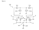
- a filter device 131 as illustrated in Fig. 14 end portions of the first LC parallel resonance circuit 7 and the second LC parallel resonance circuit 9 at the ground potential side are commonly connected.
- An inductance L23 as the sixth inductance L6 is connected between a common connection point n6 thereof and the ground potential. The connection of the inductance L23 can further increase the attenuation in the vicinity of the pass band.
- the inductance of the first LC parallel resonance circuit 7 and the inductance of the second LC parallel resonance circuit 9 are magnetically coupled, they may not be necessarily magnetically coupled.
- the elastic wave resonators used for the first and second LC parallel resonance circuits 7 and 9 are not limited to surface acoustic wave resonators; and boundary acoustic wave resonators, resonators using bulk acoustic waves, or the like may be used.
- capacitors C may be used like in the first embodiment instead of the elastic wave resonators in the first and second LC parallel resonance circuits 7 and 9. Also in this case, the attenuation in the vicinity of the pass band can be increased by the filter characteristics of the LC filter and at least one elastic wave resonator that is connected between the first and second LC parallel resonance circuits.
Landscapes
- Physics & Mathematics (AREA)
- Acoustics & Sound (AREA)
- Surface Acoustic Wave Elements And Circuit Networks Thereof (AREA)
- Filters And Equalizers (AREA)
- Piezo-Electric Or Mechanical Vibrators, Or Delay Or Filter Circuits (AREA)
Abstract
Description
- The present invention relates to a band pass filter device, more specifically, relates to a filter device using an LC parallel resonance circuit and an elastic wave resonator.
- Various existing filter devices have been proposed as band pass filters for mobile communication devices and the like. A pass band of the filter device of this type is required to be wide in many cases.
- The following
Patent Document 1 discloses a band pass filter device capable of widening a pass band. In the band pass filter device as disclosed inPatent Document 1, a high pass filter circuit and a low pass filter circuit are connected in series. The high pass filter circuit includes a high pass surface acoustic wave resonator and a high pass inductance element that is connected in parallel with the high pass surface acoustic wave resonator. On the other hand, the low pass filter circuit includes a first surface acoustic wave resonator that is arranged on a serial arm and one end of which is connected to an end portion of the high-pass filter circuit. - A second surface acoustic wave resonator is connected between the one end of the first surface acoustic wave resonator and a ground potential and a low pass inductance element is connected in parallel with the second elastic wave resonator. Further, the second surface acoustic wave resonator is also connected between the other end of the above-mentioned first surface acoustic wave resonator and the ground potential. A low pass inductance element is also connected in parallel with the second surface acoustic wave resonator.
- The following
Patent Document 2 discloses a surface acoustic wave (SAW) filter having a wide pass band in a digital terrestrial television (TV) radio wave band. In the SAW filter as disclosed inPatent Document 2, two serial arm resonators are provided on a serial arm connecting an input terminal and an output terminal. Inductance for shifting resonant frequency/anti-resonant frequency is connected between the two serial arm resonators in series to the two serial arm resonators. - Further, a parallel arm resonator is arranged on a parallel arm connecting the input terminal and a ground potential. An inductance element is connected in parallel with the parallel arm resonator. In the same manner, a parallel arm resonator is also provided on a parallel arm connecting the output terminal and the ground potential. An inductance element is also connected in parallel with the parallel arm resonator.
- The inductance element connected to each of the above-mentioned parallel arm resonators is provided for shifting a resonant frequency and an anti-resonant frequency by the parallel arm resonator.
-
- Patent Document 1: Japanese Unexamined Patent Application Publication No.
2011-234191 - Patent Document 2: Japanese Unexamined Patent Application Publication No.
2007-202136 - In
Patent Document 1 andPatent Document 2, as described above, the resonant frequency or the anti-resonant frequency of the surface acoustic wave resonator arranged on a line connecting the input terminal and the output terminal, in other words, the serial arm, or of the surface acoustic wave resonator arranged on the parallel arm connecting the line and the ground potential can be adjusted. This adjustment widens the band, improves attenuation characteristics, and so on. - It has been, however, difficult to further widen the pass band with the band pass filter using the surface acoustic wave resonator. For example, in a ladder circuit, the resonant frequency of the parallel arm resonator and the anti-resonant frequency of the serial arm resonator form attenuation poles at the low-frequency region side and the high-frequency region side. Accordingly, it is sufficient that they are distanced from each other in order to widen the band. However, when a difference in frequency between the attenuation pole at the low-frequency region side and the attenuation pole at the high-frequency region side is made larger, there arises a problem that attenuation at the center of the pass band is increased. Accordingly, widening of the band has been limiting.
- In addition, the ladder filter device also has a problem that attenuation in an attenuation band separated from the attenuation pole is not sufficiently large.
- An object of the present invention is to provide a filter device capable of further widening a band and sufficiently increasing attenuation in an attenuation region separated from a pass band.
- According to an aspect of the present invention, there is provided a filter device that includes an input terminal, an output terminal, a line connecting the input terminal and the output terminal, a first LC parallel resonance circuit connected between the line and a ground potential and including a first inductance, a second LC parallel resonance circuit connected between the line and the ground potential and including a second inductance, and at least one elastic wave resonator connected between an end portion of the first LC parallel resonance circuit at the line side and an end portion of the second LC parallel resonance circuit at the line side. In the filter device, the first and second LC parallel resonance circuits are electrically coupled by a capacitive property of the at least one elastic wave resonator, and attenuation-frequency characteristics of an LC filter formed by the first and second LC parallel resonance circuits and the capacitive property of the at least one elastic wave resonator and attenuation-frequency characteristics formed by an anti-resonance point of the elastic wave resonator are combined.
- According to another broad aspect of the invention, there is provided a filter device that includes an input terminal, an output terminal, a line connected to the input terminal and the output terminal, a first LC parallel resonance circuit connected between the line and a ground potential, including a first inductance, and having a first parallel resonant frequency, a second LC parallel resonance circuit connected between the line and the ground potential, including a second inductance, and having a second parallel resonant frequency, and a filter circuit including at least one elastic wave resonator connected to an end portion of the first LC parallel resonance circuit at the line side and an end portion of the second LC parallel resonance circuit at the line side. In the filter device, first resonance characteristics of the first LC parallel resonance circuit, second resonance characteristics of the second LC parallel resonance circuit, and a capacitive property of the at least one elastic wave resonator cause the first and second resonance characteristics to be electrically coupled so as to form pass band characteristics of an LC filter. Further, a pass band of the LC filter is arranged in a frequency region that is lower than an anti-resonant frequency of the at least one elastic wave resonator or higher than a resonant frequency thereof, the first parallel resonant frequency and the second parallel resonant frequency are arranged in the pass band of the LC filter, and an attenuation pole of the filter circuit including the at least one elastic wave resonator is arranged in an attenuation region at an outside of the pass band of the LC filter.
- In a specific aspect of the filter device according to the invention, the first inductance in the first LC parallel resonance circuit and the second inductance in the second LC parallel resonance circuit are magnetically coupled.
- In another specific aspect of the filter device according to the invention, the at least one elastic wave resonator connected between the first LC parallel resonance circuit and the second LC parallel resonance circuit is formed with a plurality of elastic wave resonators and the plurality of elastic wave resonators configure a ladder filter circuit.
- In still another specific aspect of the filter device according to the invention, the first and second LC parallel resonance circuits are respectively formed by the first and second inductances and second and third elastic wave resonators connected in parallel with the first and second inductances, and capacitive properties of the second and third elastic wave resonators configure capacitors of the first and second LC parallel resonance circuits, respectively.
- In another specific aspect of the filter device according to the invention, a circuit portion in which the first inductance in the first LC parallel resonance circuit and the second inductance in the second LC parallel resonance circuit are magnetically coupled is configured by a circuit formed in a delta-shaped manner including the first inductance, the second inductance, and a third inductance connecting one end of the first inductance and one end of the second inductance.
- In still another specific aspect of the filter device according to the invention, a circuit portion in which the first inductance in the first LC parallel resonance circuit and the second inductance in the second LC parallel resonance circuit are magnetically coupled is configured by a three-element Y type circuit including a common inductance serving as the first inductance and the second inductance, a fourth inductance connected to a connection point between an end portion of the common inductance at a side opposite to a ground potential and the input terminal, and a fifth inductance connected between the connection point and the output terminal.
- In still another specific aspect of the filter device according to the invention, each of the first inductance and the second inductance in the first and second LC parallel resonance circuits is divided in series into a plurality of inductances.
- In still another specific aspect of the filter device according to the invention, each of the first and second capacitors in the first LC parallel resonance circuit and the second LC parallel resonance circuit is formed by a plurality of elastic wave resonators connected in series.
- In still another specific aspect of the filter device according to the invention, a sixth inductance is connected between an ground potential and an end portion of at least one LC parallel resonance circuit of the first and second LC parallel resonance circuits at the ground potential side.
- In the filter device according to the invention, a surface acoustic wave resonator can be preferably used as the above-mentioned elastic wave resonator. It is needless to say that the elastic wave resonator may be a resonator using bulk acoustic waves. Further, a boundary acoustic wave resonator using boundary acoustic waves may be used.
- With the filter device according to the invention, a wide pass band can be obtained and attenuation in an attenuation band separated from the pass band can be sufficiently increased. Further, attenuation in the vicinity of the pass band can be sufficiently increased.
-
- [
Fig. 1] Fig. 1(a) and Fig. 1(b) are a circuit diagram of a filter device according to a first embodiment of the invention and a schematic plan view of an electrode configuration of a surface acoustic wave resonator, respectively. - [
Fig. 2 ]Fig. 2(a) is a schematic block diagram of the filter device in the first embodiment,Fig. 2(b) is a schematic block diagram when the filter device in the embodiment operates as an LC filter, andFig. 2(c) is a schematic block diagram when an elastic wave resonator arranged on a line connecting an input terminal and an output terminal of the filter device in the embodiment operates. - [
Fig. 2A] Fig. 2A(a) is a graph illustrating attenuation-frequency characteristics of an existing LC filter when anelastic wave resonator 21 is taken as a capacitor, and attenuation-frequency characteristics of the elastic wave resonator,Fig. 2A(b) is a graph illustrating attenuation-frequency characteristics of the filter device in the first embodiment, andFig. 2A(c) is a graph illustrating attenuation-frequency characteristics when negative magnetic coupling is formed in the filter device in the first embodiment. - [
Fig. 3] Fig. 3 is a circuit diagram of a filter device according to a second embodiment of the invention. - [
Fig. 4] Fig. 4 is a circuit diagram of a filter device according to a third embodiment of the invention. - [
Fig. 5] Fig. 5(a) is a graph for explaining attenuation-frequency characteristics of a ladder circuit portion and an LC filter portion,Fig. 5(b) is a graph illustrating attenuation-frequency characteristics of the filter device in the third embodiment,Fig. 5(c) is a graph illustrating attenuation-frequency characteristics of the filter device when positive magnetic coupling is formed in the third embodiment, andFig. 5(d) is a graph illustrating attenuation-frequency characteristics of the filter device when negative magnetic coupling is formed in the third embodiment. - [
Fig. 6] Fig. 6 is a circuit diagram of a filter device according to a fourth embodiment of the invention. - [
Fig. 7] Fig. 7 is a circuit diagram of a filter device according to a variation of the third embodiment of the invention. - [
Fig. 8] Fig. 8 is a graph illustrating attenuation-frequency characteristics in the variation as illustrated inFig. 7 . - [
Fig. 9] Fig. 9 is a circuit diagram of a filter device according to a fifth embodiment of the invention. - [
Fig. 10] Fig. 10 is a circuit diagram of a filter device according to a sixth embodiment of the invention. - [
Fig. 11] Fig. 11 is a circuit diagram of a filter device according to a seventh embodiment of the invention. - [
Fig. 12] Fig. 12 is a circuit diagram of a filter device according to an eighth embodiment of the invention. - [
Fig. 13] Fig. 13 is a circuit diagram of a filter device according to a ninth embodiment of the invention. - [
Fig. 14] Fig. 14 is a circuit diagram of a filter device according to a tenth embodiment of the invention. - Hereinafter, the present invention is made clear by describing specific embodiments of the invention with reference to the drawings
-
Fig. 1(a) is a circuit diagram of a filter device according to a first embodiment of the invention. - A
filter device 1 includes aninput terminal 2 and anoutput terminal 3. A first LCparallel resonance circuit 7 is connected between aconnection point 5 between theinput terminal 2 and anelastic wave resonator 21 and a ground potential. The first LCparallel resonance circuit 7 includes an inductance L1 and a capacitor C1 connected in parallel with the inductance L1. - A second LC
parallel resonance circuit 9 is connected between aconnection point 6 between theoutput terminal 3 and theelastic wave resonator 21 and the ground potential. The second LCparallel resonance circuit 9 includes an inductance L2 and a capacitor C2 connected in parallel with the inductance L2. - The
elastic wave resonator 21 is connected between an end portion of the first LCparallel resonance circuit 7 at theinput terminal 2 side and an end portion of the second LCparallel resonance circuit 9 at theoutput terminal 3 side so as to form a filter circuit. In the embodiment, oneelastic wave resonator 21 is connected. Resonance points of the first and second LC parallel resonance circuits are set to be close to the center frequency of a pass band of thefilter device 1. - Not one but a plurality of elastic wave resonators may be connected. In this case, a connection mode of the plurality of elastic wave resonators is not particularly limited.
- In the embodiment, the
elastic wave resonator 21 is formed by a surface acoustic wave resonator.Fig. 1(b) schematically illustrates an electrode configuration of theelastic wave resonator 21 formed by the surface acoustic wave resonator. Theelastic wave resonator 21 includes an interdigital transducer (IDT)electrode 22 andreflectors IDT electrode 22 in a propagation direction of the surface acoustic waves. Although the electrode configuration of theelastic wave resonator 21 is not particularly limited, a normal one-port surface acoustic wave resonator like this one can be preferably used therefor. It should be noted that thereflectors - Preferably, it is desired that the above-mentioned inductance L1 and inductance L2 are magnetically coupled as indicated by a dashed line M in
Fig. 1(a) . The magnetic coupling makes the circuit equivalent to a circuit in which the magnetically coupled inductance is connected to the line connected to theinput terminal 2 and theoutput terminal 3. That is to say, the circuit becomes equivalent to a circuit in which the inductance equivalent in the circuit as described above is connected in parallel with theelastic wave resonator 21. Accordingly, the magnetic coupling makes the circuit equivalent to a circuit in which an LC parallel resonance circuit is configured in frequency regions where theelastic wave resonator 21 mainly operates to exhibit a capacitive property. The frequency regions where theelastic wave resonator 21 mainly operates to exhibit the capacitive property are frequency regions other than the resonant frequency and the anti-resonant frequency of the elastic wave resonator and a frequency region between the resonant frequency and the anti-resonant frequency of the elastic wave resonator. In the frequency regions where theelastic wave resonator 21 mainly operates to exhibit the capacitive property, the above-mentioned LC parallel resonance circuit is configured, so that as indicated by a dashed line A1 inFig. 5(c) or a dashed line A2 inFig. 5(d) , an attenuation pole by the resonant frequency by the LC parallel resonance circuit can be formed in an attenuation region part separated from the pass band. Accordingly, the attenuation in the attenuation region separated from the pass band can be further increased. - Widening of the band, increase of the attenuation in the vicinity of the pass band, and increase of the attenuation in the attenuation region separated from the pass band that can be achieved by the
filter device 1 in the invention, are described with reference toFigs. 2 andFigs. 2A . -
Fig. 2(a) is a schematic block diagram of the filter device according to the first embodiment as illustrated inFigs. 1 . As illustrated in the schematic block diagram, the first LCparallel resonance circuit 7 is connected between the line connecting theinput terminal 2 and theoutput terminal 3 and the ground potential. The second LCparallel resonance circuit 9 is connected between the ground potential and the line connecting theinput terminal 2 and theoutput terminal 3 at theoutput terminal 3 side relative to the first LCparallel resonance circuit 7. Theelastic wave resonator 21 is connected between the connection points at which the first LCparallel resonance circuit 7 and the second LCparallel resonance circuit 9 are respectively connected to the line. - As the frequency characteristics of the
elastic wave resonator 21, theelastic wave resonator 21 mainly exhibits an inductive property in the frequency region between the resonant frequency and the anti-resonant frequency and mainly exhibits a capacitive property in a frequency region lower than the resonant frequency and in a frequency region higher than the anti-resonant frequency. Accordingly, in the frequency regions where theelastic wave resonator 21 exhibits the capacitive property, the block diagram of thefilter device 1 corresponds toFig. 2(b) . That is to say, in the frequency regions where theelastic wave resonator 21 mainly exhibits the capacitive property, an LC filter in which the first and second LCparallel resonance circuits Fig. 2(b) is configured. A solid line inFig. 2A(a) indicates attenuation-frequency characteristics of the above-mentioned LC filter. In the LC filter, a pass band wider than that of a ladder filter using a plurality of surface acoustic wave resonators can be obtained. That is to say, even when the pass band is widened by adjusting values of the inductances and the capacitor, it is difficult to increase the attenuation at the center of the pass band. - As indicated by the solid line in
Fig. 2A(a) , inclinations of the attenuation characteristics from the pass band toward the outsides of the pass band are moderate in the LC filter. - In the embodiment, the above-mentioned
elastic wave resonator 21 is provided. The resonant frequency of theelastic wave resonator 21 is within the pass band of thefilter device 1 as described above. The anti-resonant frequency thereof is located at a portion on which the attenuation is desired to be increased, to be more specific, in the vicinity of the pass band and within the attenuation region at the high-frequency region side relative to the pass band. - On the other hand, the above-mentioned
elastic wave resonator 21 mainly exhibits the inductive property between the resonant frequency and the anti-resonant frequency. The attenuation-frequency characteristics as indicated by a dashed line inFig. 2A(a) are characteristics in a frequency region including therein the resonant frequency and the anti-resonant frequency of theelastic wave resonator 21. Thefilter device 1 in the embodiment in which the LC filter and theelastic resonator 21 are combined using the above-mentioned frequency characteristics has attenuation-frequency characteristics including the attenuation-frequency characteristics as indicated by the solid line inFig. 2A(a) and the attenuation-frequency characteristics as indicated by the dashed line inFig. 2A(a) in combination. Accordingly, the attenuation-frequency characteristics of thefilter device 1 in the embodiment as illustrated inFig. 2A(b) are obtained. That is to say, the attenuation-frequency characteristics of the above-mentionedelastic wave resonator 21 connected between theinput terminal 2 and theoutput terminal 3 are used, which serves as a filter circuit as illustrated inFig. 2(c) , which is configured such that it has the anti-resonant frequency as indicated by the dashed line inFig. 2A(a) and the attenuation frequency changes in accordance with a predetermined frequency as illustrated inFig. 2A(b) . - In the embodiment, the attenuation characteristics of the LC filter in which the LC parallel resonance circuits are configured can be made steeper than the attenuation characteristics of the LC filter as indicated by the solid line in
Fig. 2A(a) by the filter characteristics of theelastic wave resonator 21, which makes use of resonance by elastic waves, that change including the anti-resonance point in accordance with the predetermined frequency. Accordingly, in thefilter device 1, the attenuation characteristics at the high-frequency side of the pass band can be made steep as illustrated inFig. 2A(b) . Further, the attenuation in the attenuation region in the vicinity of the pass band can be increased due to impedance characteristics at the anti-resonant frequency of theelastic wave resonator 21. - In addition, as is obvious from a portion indicated by the dashed line in
Fig. 2A(a) , if the frequency of theelastic wave resonator 21 is further shifted toward the high-frequency region side relative to the anti-resonant frequency at which the attenuation pole is formed, the attenuation of theelastic wave resonator 21 is decreased. This raises a problem that the attenuation in the attenuation region separated from the pass band is not sufficiently decreased in the ladder filter and the like including the elastic wave resonator. In contrast, because the filter characteristics of the above-mentioned LC filter are used in the embodiment, the attenuation in the attenuation region separated from the pass band can be increased. With the filter characteristics of the LC filter, the attenuation is large in the attenuation region separated from the pass band. Accordingly, in the embodiment, the attenuation in the attenuation band separated from the pass band can be also increased. - It is sufficient that a relationship between a minimum signal intensity A in a predetermined frequency band of the filter device and a signal intensity B continuous to the signal intensity A is set as follows. That is, a frequency region in which a calculation result of 10Log10 B/A is higher than -3 [dB] is taken as the pass band and a frequency region in which the calculation result of 10Log10 B/A is equal to or lower than -3 [dB] is taken as the attenuation band. The signal intensity can be calculated from a voltage value of the filter device.
- As described above, the
filter device 1 in the embodiment has a configuration capable of widening the pass band and enlarging the attenuation band separated from the pass band by the LC filter, and increasing the attenuation in the vicinity of the pass band using theelastic wave resonator 21. That is to say, thefilter device 1 in the embodiment has a configuration capable of utilizing both the advantages of the characteristics of the LC filter and the elastic wave resonator while they are not obstructed by each other. - In the above-mentioned embodiment, an anti-resonant frequency fa of the
elastic wave resonator 21 is located at the high-frequency side relative to an end portion of the pass band formed by the LC filter at the high-frequency region side. With this, the attenuation characteristics at the high-frequency region side of the pass band is drastically steepened. Thus, in order to drastically steepen the attenuation characteristics at the high-frequency region side of the pass band, it is sufficient that the anti-resonant frequency fa is set to a position at which the attenuation pole is desired to be formed for providing the attenuation pole in the vicinity of the end portion of the pass band at the high-frequency region side. In other words, when fa > fh > f0 is satisfied (note that fh is a frequency at the end portion of the pass band at the high-frequency region side and f0 is the center frequency of the pass band formed by the LC filter), the characteristics at the high-frequency region side of the pass band can be drastically steepened. - When the center frequencies of the pass bands of the LC resonance circuits, which correspond to the first LC resonant frequency of the first LC
parallel resonance circuit 7 and the second LC resonant frequency of the second LCparallel resonance circuit 9, are set to f1 and f2, respectively, it is preferable for f0, f1, and f2 to be close to one another, and it is also preferable to be f0=f1=f2. It is needless to say that the center frequency f1 and the center frequency f2 are not necessarily equal to each other. - Unlike the above-mentioned case, in order to drastically steepen the attenuation characteristics at the low-frequency region side of the pass band, it is sufficient that the anti-resonant frequency fa of the
elastic wave resonator 21 is located in the attenuation band in the vicinity of the end portion of the pass band at the low-frequency region side. With this, the attenuation characteristics in the attenuation region in the vicinity of the pass band at the low-frequency region side can be drastically steepened. In this case, it is sufficient that the anti-resonant frequency fa is lower than fl (frequency of the end portion of the pass band at the low-frequency region side). - In the LC parallel resonance circuit as illustrated in
Fig. 1(a) , when predetermined magnetic coupling is formed by the first inductor L1 and the second inductor L2, an attenuation pole is generated at an outside of the pass band at the high-frequency region side as illustrated inFig. 2A(c) and the attenuation is increased. The filter characteristics with the magnetic coupling that is formed in thefilter device 1 can be replaced by the filter characteristics of a circuit in which an equivalent inductor is connected in parallel with the filter circuit. It is considered that the attenuation pole generated by LC parallel resonance by the equivalent inductor and the capacitive property of the elastic wave resonator can increase the attenuation at the outside of the pass band at the high-frequency region side as illustrated inFig. 2A(c) . -
Fig. 3 is a circuit diagram of a filter device according to a second embodiment of the invention. As in thefilter device 1 in the first embodiment, afilter device 51 includes the first LCparallel resonance circuit 7, the second LCparallel resonance circuit 9, and theelastic wave resonator 21. - A different point is that second and third elastic wave resonators P1 and P2 are used instead of the capacitors C1 and C2 in the first embodiment, respectively. The resonant frequencies of the elastic wave resonators P1 and P2 are at the low-frequency region side of the pass band and the anti-resonant frequencies thereof are within the pass band. The elastic wave resonators P1 and P2 and the
elastic wave resonator 21 mainly operate to exhibit a capacitive property in a frequency band at the low-frequency region side relative to the resonant frequency and a frequency band at the high-frequency region side relative to the anti-resonant frequency. Accordingly, also in the embodiment, the filter characteristics of the LC filter by the first and second LCparallel resonance circuits -
Fig. 4 is a circuit diagram of a filter device according to a third embodiment of the invention. In afilter device 61, the first and second LCparallel resonance circuits - The third embodiment is different from the second embodiment in a point that a
ladder filter circuit 62 is connected instead of theelastic wave resonator 21. Theladder filter circuit 62 includes a plurality of serial arm resonators S11 to S1n (note that n is a positive integer) arranged on a serial arm connecting theinput terminal 2 and theoutput terminal 3 and parallel arm resonators P11 to P1m (note that m is a positive integer). - Thus, the plurality of elastic wave resonators may be connected between the first LC
parallel resonance circuit 7 and the second LCparallel resonance circuit 9, and it is desirable that the plurality of elastic wave resonators configure theladder filter circuit 62 as in the embodiment. - In the embodiment, the filter characteristics of the LC filter by the first and second LC
parallel resonance circuits Fig. 2A(a) indicates attenuation-frequency characteristics of an existing LC filter in which theelastic wave resonator 21 illustrated in the schematic block diagram ofFig. 2(a) is a capacitor, and a dashed line inFig. 5(a) indicates filter characteristics of theladder filter circuit 62.Fig. 5(b) illustrates the attenuation-frequency characteristics of the filter device in the embodiment, which includes theladder filter circuit 62 configured by the plurality of elastic wave resonators. As the attenuation-frequency characteristics are compared usingFig. 5(b) and Fig. 5(a) , it is found that 1) widening of the band and 3) increase of the attenuation in the attenuation band separated from the pass band can be achieved in the embodiment. - In addition, the
ladder filter circuit 62 is provided so as to increase the attenuation in the vicinity of the pass band. To be more specific, the resonant frequencies of the parallel arm resonators P11 to P1m of theladder filter circuit 62 are made to match the attenuation pole located at an outside of the pass band of thefilter device 61 at the low-frequency region side, and the anti-resonant frequencies thereof are located in the pass band of thefilter device 61. The resonant frequencies of the serial arm resonators S11 to S1n are located in the pass band of thefilter device 61 at the high-frequency region side, and the anti-resonant frequencies thereof are set to the attenuation pole located at an outside of the pass band at the high-frequency region side. With this, theladder filter circuit 62 having the attenuation poles in the frequency bands in the vicinity of the end portions of the pass band of thefilter device 61 at the low-frequency region side and the high-frequency region side as the attenuation-frequency characteristics of theladder filter circuit 62 as indicated by the solid line inFig. 5(a) can be obtained. In the frequency band lower than the anti-resonant frequencies of the parallel arm resonators and higher than the resonant frequencies of the serial arm resonators, thefilter device 61 having low attenuation at the center and a wide pass band can be obtained using the filter characteristics as the LC filter obtained by the configuration of the capacitive properties of the parallel arm and serial arm resonators of theladder filter circuit 62 and the first and second LCparallel resonance circuits - Accordingly, with the configuration of the
filter device 61, the attenuation-frequency characteristics as illustrated inFig. 5(b) in which the center frequency of the pass band is approximately 2.6 GHz, the band width of the pass band is approximately 200 MHz, the attenuation is approximately 30 dB at the frequency of approximately 2.4 GHZ in the vicinity of the pass band at the low-frequency region side, and the attenuation is approximately 50 dB at the frequency of approximately 2.8 GHZ in the vicinity of the pass band at the high-frequency region side are obtained by combining the filter characteristics of the first and second LCparallel resonance circuits ladder filter circuit 62 having the attenuation poles in predetermined frequency bands. That is to say, as illustrated inFig. 5(b) , in the embodiment, 1) widening of the band, 2) increase of the attenuation in the vicinity of the pass band, and 3) increase of the attenuation in the attenuation band separated from the pass band can be achieved. - Further, in a variation of the third embodiment of the invention, when the inductance L1 and the inductance L2 form positive magnetic coupling, as indicated by a dashed line A1 in
Fig. 5(c) , the attenuation pole by the magnetic coupling can be arranged at an outside of the pass band of the filter device at the low-frequency region side. On the other hand, when the inductance L1 and the inductance L2 form negative magnetic coupling, as indicated by a dashed line A2 inFig. 5(d) , the attenuation pole by the magnetic coupling can be arranged in the pass band of the filter device at the high-frequency region side. The attenuation pole by the magnetic coupling, which is arranged at the outside of the pass band at the low-frequency region side or the high-frequency region side, can further increase the attenuation at the outside of the pass band in comparison with the case where the magnetic coupling is not formed. When an electric current I1 of an angular frequency ω flows through the inductance L1, an electric current I2 of the angular frequency ω is generated in the inductance L2 arranged in the vicinity of the inductance L1 by mutual inductance. When a mutual relationship such that the generated magnetic flux strengthens each other is established between the inductance L1 and the inductance L2, that is, when a value of M is positive in thefollowing equation 1 and thefollowing equation 2 under an assumption that a voltage of the inductance L1 is taken as V1 and a voltage of the inductance L2 is taken as V2, it is considered that positive magnetic coupling is formed. In contrast, when a mutual relationship such that the generated magnetic flux weakens each other is established between the inductance L1 and the inductance L2, that is, when the value of M is negative in thefollowing equation 1 and thefollowing equation 2, it is considered that negative magnetic coupling is formed.

-
Fig. 6 is a circuit diagram of a filter device according to a fourth embodiment of the invention. Afilter device 71 includes the first LCparallel resonance circuit 7 connected to theinput terminal 2 and the second LCparallel resonance circuit 9 connected to theoutput terminal 3. In addition, aladder filter circuit 72 is connected between the first LCparallel resonance circuit 7 and the second LCparallel resonance circuit 9. Theladder filter circuit 72 includes a plurality of serial arm resonators S21 to S2n (note that n is a positive integer) and a plurality of parallel arm resonators P21 to P2m (note that m a positive integer). Also in the embodiment, the first LCparallel resonance circuit 7 and the second LCparallel resonance circuit 9 have the same configurations as those in the third embodiment. Theladder filter circuit 72 also has the same configuration as that of theladder filter circuit 62. - Moreover, in the embodiment, a third LC
parallel resonance circuit 73 is connected between a connection point n1 between the serial arm resonator S22 and the serial arm resonator S23 and the ground potential. The third LCparallel resonance circuit 73 includes an inductance Lx and an elastic wave resonator P3 connected in parallel with the inductance Lx. - In the embodiment, the filter characteristics of the LC filter are obtained using not only the first and second LC
parallel resonance circuits parallel resonance circuit 73. Thus, in addition to the first and second LCparallel resonance circuits parallel resonance circuits - In the embodiment, the attenuation pole at the low-frequency region side is formed by the resonant frequencies of the parallel arm resonators P21 to P2m of the
ladder filter circuit 72. Further, the attenuation pole at the high-frequency region side is formed by the anti-resonant frequencies of the serial arm resonators S21 to S2n. - Accordingly, also in the embodiment, 1) widening of the band, 2) increase of the attenuation in the vicinity of the pass band, and 3) increase of the attenuation in the attenuation band separated from the pass band can be achieved.
- It should be noted that in contrast to the above-mentioned case, the attenuation pole at the high-frequency region side may be formed by the resonant frequencies of the parallel arm resonators P21 to P2m of the
ladder filter circuit 72, and the attenuation pole at the low-frequency region side may be formed by the anti-resonant frequencies of the serial arm resonators S21 to S2n. - Also in the embodiment, preferably as indicated by arrows M, it is desirable for the inductance L1 and the inductance Lx to be magnetically coupled and the inductance Lx and the inductance L2 to be magnetically coupled. With this, the attenuation poles as indicated by the dashed line A1 in
Fig. 5(c) and the dashed line A2 inFig. 5(d) can be formed at positions separated from the pass band, so that the attenuation at the positions separated from the pass band can be further increased in comparison with the case where they are not magnetically coupled. -
Fig. 7 is a circuit diagram according to a variation of the above-mentioned third embodiment. In afilter device 61A in the variation, the same reference numerals as those inFig. 4 denote the same constituent elements thereof and description thereof is omitted. In thefilter device 61A in the variation, aladder filter circuit 62A includes the serial arm resonators S11 to S13 and the parallel arm resonators P11 and P12. Anelastic wave resonator 63 is connected between theinput terminal 2 and the first LCparallel resonance circuit 7. Anelastic wave resonator 64 is also connected between theoutput terminal 3 and the second LCparallel resonance circuit 9. Theelastic wave resonators filter device 61A is also included. - Moreover, an inductance L3 is connected between the first LC
parallel resonance circuit 7 and the second LCparallel resonance circuit 9. Further, the inductance L1 and the inductance L2 are magnetically coupled. -
Fig. 8 is a graph illustrating the attenuation-frequency characteristics of thefilter device 61A in the variation. In the variation, filter characteristics used for a filter satisfying the BAND41 standard of the universal mobile telecommunications system (UMTS) are obtained. In this case, the pass band is from 2496 to 2690 MHz, and the bands in which large attenuation is desired to be ensured are a band of 2400 to 2473 MHz in the IMS band of 2.4 GHz and a band of 800 to 2170 MHz in the UMTS band. As is obvious fromFig. 8 , widening of the band and increase of the attenuation in the vicinity of the pass band can be achieved. - Further, because the above-mentioned
elastic wave resonators Fig. 8 . With this, the attenuation at the position separated from the pass band is increased and the impedance of the filter circuit can be adjusted. - A resonant frequency Fx that is generated by resonance among the equivalent inductance due to the magnetic coupling between the inductance L1 and the inductance L2, the inductance L3, and a capacitive component of the ladder circuit, appears at a position indicated by an arrow X at the low-frequency region side relative to the pass band. Accordingly, the attenuation is increased at the position indicated by the arrow X.
-
Fig. 9 is a circuit diagram of a filter device according to a fifth embodiment of the invention. Afilter device 81 in the fifth embodiment corresponds to the variation of thefilter device 61 in the third embodiment. Thefilter device 81 is different from thefilter device 61 in the third embodiment in a point that the first inductance L1 and the second inductance L2 are connected to the third inductance L3 connected between the first and second LCparallel resonance circuits - Thus, the third inductance L3 may be connected instead of the magnetic coupling between the inductance L1 and the inductance L2. That is to say, a circuit formed in a delta-shaped manner that is equivalent to the circuit in which the first and second inductances L1 and L2 are magnetically coupled may be used.
-
Fig. 10 is a circuit diagram illustrating a filter device according to a sixth embodiment of the invention. Afilter device 91 in the embodiment also corresponds to the variation of thefilter device 61 in the third embodiment. In thefilter device 91, the first inductance L1 and the second inductance L2 are made common and a common inductance L0 is used. That is to say, the elastic wave resonator P1 and the inductance L0 configure the first LCparallel resonance circuit 7 and the inductance L0 and the elastic wave resonator P2 configure the second LCparallel resonance circuit 9. A fourth inductance L4 is connected between the inductance L0 and the input terminal. A fifth inductance L5 is connected between one end of the inductance L0 and the output terminal. The inductances L0, L4, and L5 configure a three-element Y type circuit. The Y type circuit of this kind is equivalent to a circuit in which the inductances L1 and L2 are magnetically coupled. That is, the Y type circuit configured by the inductances L0, L4, and L5 may be used instead of the circuit formed in a delta-shaped manner as illustrated inFig. 9 . - Also with the
filter devices Fig. 9 andFig. 10 , in the same manner as thefilter device 61 in the third embodiment, 1) widening of the band, 2) increase of the attenuation in the vicinity of the pass band, and 3) increase of the attenuation in the attenuation band separated from the pass band can be achieved. In addition, the same effect as the magnetic coupling effect is achieved, so that the attenuation in the vicinity of the pass band can be further increased in comparison with the case where the circuit formed in a delta-shaped manner or the three-element Y type circuit is not formed. -
Fig. 11 to Fig. 14 are circuit diagrams of filter devices according to seventh to tenth embodiments of the invention, respectively. These filter devices also correspond to variations of thefilter device 61 in the third embodiment as illustrated inFig. 4 . Accordingly, only different portions are described hereinafter. - In a
filter device 101 as illustrated inFig. 11 , the inductance L1 and the inductance L2 are respectively divided in series in the first LCparallel resonance circuit 7 and the second LCparallel resonance circuit 9. To be specific, the inductance L1 is divided in series so that an inductance L1a and an inductance L1b are connected in series. In the same manner, inductances L2a and L2b are connected in series also in the second LCparallel resonance circuit 9. - The
input terminal 2 is connected to a connection point n2 between the inductance L1a and the inductance L1b. In the same manner, theoutput terminal 3 is connected to a connection point n3 between the inductance L2a and the inductance L2b. Thus, in the invention, the first and second inductances L1 and L2 may be divided in series. - In the same manner, like a
filter device 111 as illustrated inFig. 12 , the elastic wave resonators in the first and second LCparallel resonance circuits Fig. 12 , an elastic wave resonator P1a and an elastic wave resonator P1b are connected in series in the first LCparallel resonance circuit 7. A connection point n4 between the elastic wave resonators P1a and P1b and theinput terminal 2 are connected. In the same manner, the elastic wave resonator is also divided in series in the second LCparallel resonance circuit 9. That is to say, an elastic wave resonator P2a and an elastic wave resonator P2b are connected in series. A connection point n5 between the elastic wave resonators P2a and P2b and theoutput terminal 3 are electrically connected. - In a
filter device 121 as illustrated inFig. 13 , in the first LCparallel resonance circuit 7, an inductance L21 as a sixth inductance L6 is connected between a ground potential and end portions of the elastic wave resonator P1 and the inductance L1 at the ground potential side. In the same manner, also in the second LCparallel resonance circuit 9, an inductance L22 as the inductance L6 is connected between the ground potential and end portions of the elastic wave resonator P2 and the inductance L2 at the ground potential side. In this manner, in the first and second LCparallel resonance circuits - In a
filter device 131 as illustrated inFig. 14 , end portions of the first LCparallel resonance circuit 7 and the second LCparallel resonance circuit 9 at the ground potential side are commonly connected. An inductance L23 as the sixth inductance L6 is connected between a common connection point n6 thereof and the ground potential. The connection of the inductance L23 can further increase the attenuation in the vicinity of the pass band. - Although in the first to tenth embodiments, the inductance of the first LC
parallel resonance circuit 7 and the inductance of the second LCparallel resonance circuit 9 are magnetically coupled, they may not be necessarily magnetically coupled. - The elastic wave resonators used for the first and second LC
parallel resonance circuits - In the second to tenth embodiments, as in the first embodiment, capacitors C may be used like in the first embodiment instead of the elastic wave resonators in the first and second LC
parallel resonance circuits -
- 1 FILTER DEVICE
- 2 INPUT TERMINAL
- 3 OUTPUT TERMINAL
- 5, 6 CONNECTION POINT
- 7 FIRST LC PARALLEL RESONANCE CIRCUIT
- 9 SECOND LC PARALLEL RESONANCE CIRCUIT
- 21 ELASTIC WAVE RESONATOR
- 22 IDT ELECTRODE
- 23, 24 REFLECTOR
- 51, 61, 61A, 71, 81, 91, 101, 111, 121, 131 FILTER DEVICE
- 62, 62A, 72 LADDER FILTER CIRCUIT
- 63, 64 ELASTIC WAVE RESONATOR
- 73 THIRD LC PARALLEL RESONANCE CIRCUIT
- C1, C2 CAPACITOR
- L1, L1a, L1b FIRST INDUCTANCE
- L2, L2a, L2b SECOND INDUCTANCE
- L3 to L6 THIRD TO SIXTH INDUCTANCE
- L21 to L23 INDUCTANCE
- P1, P1a, P1b, P2, P2a, P2b, P3 ELASTIC WAVE RESONATOR
- P11 to P1m, P21 to P2m PARALLEL ARM RESONATOR
- S11 to S1n, S21 to S2n SERIAL ARM RESONATOR
Claims (12)
- A filter device comprising:an input terminal;an output terminal;a line connecting the input terminal and the output terminal;a first LC parallel resonance circuit connected between the line and a ground potential and including a first inductance;a second LC parallel resonance circuit connected between the line and the ground potential and including a second inductance; andat least one elastic wave resonator connected between an end portion of the first LC parallel resonance circuit at the line side and an end portion of the second LC parallel resonance circuit at the line side,wherein the first and second LC parallel resonance circuits are electrically coupled by a capacitive property of the at least one elastic wave resonator, andattenuation-frequency characteristics of an LC filter formed by the first and second LC parallel resonance circuits and the capacitive property of the at least one elastic wave resonator and attenuation-frequency characteristics formed by an anti-resonance point of the elastic wave resonator are combined.
- A filter device comprising:an input terminal;an output terminal;a line connected to the input terminal and the output terminal;a first LC parallel resonance circuit connected between the line and a ground potential, including a first inductance, and having a first parallel resonant frequency;a second LC parallel resonance circuit connected between the line and the ground potential, including a second inductance, and having a second parallel resonant frequency; anda filter circuit including at least one elastic wave resonator connected to an end portion of the first LC parallel resonance circuit at the line side and an end portion of the second LC parallel resonance circuit at the line side,wherein first resonance characteristics of the first LC parallel resonance circuit, second resonance characteristics of the second LC parallel resonance circuit, and a capacitive property of the at least one elastic wave resonator cause the first and second resonance characteristics to be electrically coupled so as to form pass band characteristics of an LC filter,a pass band of the LC filter is arranged in a frequency region that is lower than an anti-resonant frequency of the at least one elastic wave resonator or higher than a resonant frequency of the at least one elastic wave resonator, and the first parallel resonant frequency and the second parallel resonant frequency are arranged in the pass band of the LC filter, andan attenuation pole of the filter circuit including the at least one elastic wave resonator is arranged in an attenuation region at an outside of the pass band of the LC filter.
- The filter device according to claim 1 or 2,
wherein the first inductance included in the first LC parallel resonance circuit and the second inductance included in the second LC parallel resonance circuit are magnetically coupled. - The filter device according to any one of claims 1 to 3,
wherein the at least one elastic wave resonator connected between the first LC parallel resonance circuit and the second LC parallel resonance circuit is formed with a plurality of elastic wave resonators and the plurality of elastic wave resonators configure a ladder filter circuit. - The filter device according to any one of claims 1 to 4,
wherein the first and second LC parallel resonance circuits are respectively formed by the first and second inductances and second and third elastic wave resonators connected in parallel with the first and second inductances, and
capacitive properties of the second and third elastic wave resonators configure capacitors of the first and second LC parallel resonance circuits, respectively. - The filter device according to claim 3,
wherein a circuit portion in which the first inductance in the first LC parallel resonance circuit and the second inductance in the second LC parallel resonance circuit are magnetically coupled is configured by a circuit formed in a delta-shaped manner including the first inductance, the second inductance, and a third inductance connecting one end of the first inductance and one end of the second inductance. - The filter device according to claim 3,
wherein a circuit portion in which the first inductance in the first LC parallel resonance circuit and the second inductance in the second LC parallel resonance circuit are magnetically coupled is configured by a three-element Y type circuit including a common induction serving as the first inductance and the second inductance, a fourth inductance connected to a connection point between an end portion of the common inductance at a side opposite to a ground potential and the input terminal, and a fifth inductance connected between the connection point and the output terminal. - The filter device according to any one of claims 1 to 7,
wherein each of the first inductance and the second inductance in the first and second LC parallel resonance circuits is divided in series into a plurality of inductances. - The filter device according to any one of claims 1 to 8,
wherein each of the first and second capacitors in the first LC parallel resonance circuit and the second LC parallel resonance circuit is formed by a plurality of elastic wave resonators connected in series. - The filter device according to any one of claims 1 to 9,
wherein a sixth inductance is connected between a ground potential and an end portion of at least one LC parallel resonance circuit of the first and second LC parallel resonance circuits at the ground potential side. - The filter device according to any one of claims 1 to 10,
wherein the elastic wave resonator is a surface acoustic wave resonator. - The filter device according to any one of claims 1 to 10,
wherein the elastic wave resonator is a resonator using bulk acoustic waves.
Applications Claiming Priority (2)
| Application Number | Priority Date | Filing Date | Title |
|---|---|---|---|
| JP2012234960 | 2012-10-24 | ||
| PCT/JP2013/071551 WO2014064987A1 (en) | 2012-10-24 | 2013-08-08 | Filter device |
Publications (2)
| Publication Number | Publication Date |
|---|---|
| EP2913923A1 true EP2913923A1 (en) | 2015-09-02 |
| EP2913923A4 EP2913923A4 (en) | 2016-06-01 |
Family
ID=50544368
Family Applications (1)
| Application Number | Title | Priority Date | Filing Date |
|---|---|---|---|
| EP13848772.3A Pending EP2913923A4 (en) | 2012-10-24 | 2013-08-08 | FILTER DEVICE |
Country Status (6)
| Country | Link |
|---|---|
| US (1) | US9509279B2 (en) |
| EP (1) | EP2913923A4 (en) |
| JP (1) | JP5896039B2 (en) |
| KR (2) | KR101989458B1 (en) |
| CN (1) | CN104737447B (en) |
| WO (1) | WO2014064987A1 (en) |
Cited By (4)
| Publication number | Priority date | Publication date | Assignee | Title |
|---|---|---|---|---|
| CN108809269A (en) * | 2017-04-26 | 2018-11-13 | Tdk株式会社 | low-pass filter |
| WO2018228771A1 (en) * | 2017-06-14 | 2018-12-20 | RF360 Europe GmbH | Electro-acoustic rf filter with increased flank steepness, multiplexer and method of designing an electro-acoustic rf filter |
| WO2019115072A1 (en) * | 2017-12-11 | 2019-06-20 | RF360 Europe GmbH | Wideband rf filter, multiband rf filter and rf filter component |
| WO2021071463A1 (en) | 2019-10-07 | 2021-04-15 | Intel Corporation | Hybrid resonators |
Families Citing this family (55)
| Publication number | Priority date | Publication date | Assignee | Title |
|---|---|---|---|---|
| DE102012112571B3 (en) * | 2012-12-18 | 2014-06-05 | Epcos Ag | circuitry |
| DE112015003080B4 (en) | 2014-06-30 | 2018-06-21 | Snaptrack, Inc. | RF FILTER CIRCUIT, RF FILTER WITH IMPROVED DAMPING AND DUPLEXER WITH IMPROVED INSULATION |
| US10333494B2 (en) | 2014-12-24 | 2019-06-25 | Qorvo Us, Inc. | Simplified acoustic RF resonator parallel capacitance compensation |
| US9837984B2 (en) | 2014-12-24 | 2017-12-05 | Qorvo Us, Inc. | RF ladder filter with simplified acoustic RF resonator parallel capacitance compensation |
| JP6531824B2 (en) * | 2015-04-17 | 2019-06-19 | 株式会社村田製作所 | Resonant circuit, band rejection filter and band pass filter |
| US9847769B2 (en) | 2015-09-25 | 2017-12-19 | Qorvo Us, Inc. | Tunable compensation circuit for filter circuitry using acoustic resonators |
| US10097161B2 (en) | 2015-09-25 | 2018-10-09 | Qorvo Us, Inc. | Compensation circuit for acoustic resonators |
| US9762208B2 (en) | 2015-09-30 | 2017-09-12 | Avago Technologies General Ip (Singapore) Pte. Ltd. | Very wide bandwidth composite bandpass filter with steep roll-off |
| US9893713B2 (en) | 2015-09-30 | 2018-02-13 | Avago Technologies General Ip (Singapore) Pte. Ltd. | Wide bandwidth muliplexer based on LC and acoustic resonator circuits for performing carrier aggregation |
| US10263599B2 (en) * | 2015-12-21 | 2019-04-16 | Qorvo Us, Inc. | Bulk acoustic wave (BAW) filter with coupled inductors |
| US10243537B2 (en) | 2016-01-12 | 2019-03-26 | Qorvo Us, Inc. | Compensation circuit for use with acoustic resonators to provide a bandstop |
| JP6743396B2 (en) * | 2016-01-25 | 2020-08-19 | Tdk株式会社 | Bandpass filters and duplexers |
| CN109075771B (en) * | 2016-04-08 | 2022-08-16 | 谐振公司 | Radio frequency filter, high selectivity triplexer and communication apparatus |
| US10141644B2 (en) | 2016-04-18 | 2018-11-27 | Qorvo Us, Inc. | Acoustic filter for antennas |
| US10581156B2 (en) | 2016-05-04 | 2020-03-03 | Qorvo Us, Inc. | Compensation circuit to mitigate antenna-to-antenna coupling |
| US10581403B2 (en) | 2016-07-11 | 2020-03-03 | Qorvo Us, Inc. | Device having a titanium-alloyed surface |
| CN109690944B (en) * | 2016-09-07 | 2023-02-28 | 株式会社村田制作所 | Elastic wave filter device and composite filter device |
| US11050412B2 (en) | 2016-09-09 | 2021-06-29 | Qorvo Us, Inc. | Acoustic filter using acoustic coupling |
| US10284174B2 (en) | 2016-09-15 | 2019-05-07 | Qorvo Us, Inc. | Acoustic filter employing inductive coupling |
| US10367470B2 (en) | 2016-10-19 | 2019-07-30 | Qorvo Us, Inc. | Wafer-level-packaged BAW devices with surface mount connection structures |
| WO2018096799A1 (en) * | 2016-11-22 | 2018-05-31 | 株式会社村田製作所 | Filter device and multiplexer |
| US11165412B2 (en) | 2017-01-30 | 2021-11-02 | Qorvo Us, Inc. | Zero-output coupled resonator filter and related radio frequency filter circuit |
| US11165413B2 (en) | 2017-01-30 | 2021-11-02 | Qorvo Us, Inc. | Coupled resonator structure |
| WO2018159205A1 (en) * | 2017-02-28 | 2018-09-07 | 株式会社村田製作所 | Filter device, multiplexer, high-frequency front end circuit, and communication apparatus |
| US10873318B2 (en) | 2017-06-08 | 2020-12-22 | Qorvo Us, Inc. | Filter circuits having acoustic wave resonators in a transversal configuration |
| JP6708177B2 (en) * | 2017-07-21 | 2020-06-10 | 株式会社村田製作所 | High frequency filter, multiplexer, high frequency front end circuit and communication device |
| WO2019021983A1 (en) * | 2017-07-25 | 2019-01-31 | 株式会社村田製作所 | High frequency filter, multiplexer, high frequency front-end circuit, and communication device |
| US10931263B2 (en) * | 2017-08-03 | 2021-02-23 | Qorvo Us, Inc. | Filter circuits having a resonator-based filter and a magnetically-coupled filter |
| US10141907B1 (en) * | 2017-08-25 | 2018-11-27 | Psemi Corporation | Integrated BPF and LNA input match |
| US10361676B2 (en) | 2017-09-29 | 2019-07-23 | Qorvo Us, Inc. | Baw filter structure with internal electrostatic shielding |
| JP6959819B2 (en) | 2017-10-02 | 2021-11-05 | 株式会社村田製作所 | Multiplexer |
| US11152913B2 (en) | 2018-03-28 | 2021-10-19 | Qorvo Us, Inc. | Bulk acoustic wave (BAW) resonator |
| KR20190122493A (en) * | 2018-04-20 | 2019-10-30 | 삼성전기주식회사 | High pass filter |
| DE102019210496A1 (en) | 2018-07-18 | 2020-01-23 | Skyworks Solutions, Inc. | HYBRID ACOUSTIC LC FILTER WITH HARMONIC SUPPRESSION |
| JP2020108066A (en) | 2018-12-28 | 2020-07-09 | 株式会社村田製作所 | Filter circuit and filter device |
| CN110071702B (en) * | 2019-02-19 | 2023-04-07 | 天津大学 | Band-pass filter and duplexer |
| CN109672422B (en) * | 2019-02-22 | 2023-08-25 | 安徽安努奇科技有限公司 | filter circuit and multiplexer |
| JP7232083B2 (en) * | 2019-03-05 | 2023-03-02 | 太陽誘電株式会社 | filter |
| US11146247B2 (en) | 2019-07-25 | 2021-10-12 | Qorvo Us, Inc. | Stacked crystal filter structures |
| CN111600574B (en) * | 2019-08-30 | 2023-10-03 | 天津大学 | Bulk acoustic wave filter and out-of-band suppression improvement method thereof |
| US11757430B2 (en) | 2020-01-07 | 2023-09-12 | Qorvo Us, Inc. | Acoustic filter circuit for noise suppression outside resonance frequency |
| US11146245B2 (en) | 2020-01-13 | 2021-10-12 | Qorvo Us, Inc. | Mode suppression in acoustic resonators |
| US11146246B2 (en) | 2020-01-13 | 2021-10-12 | Qorvo Us, Inc. | Phase shift structures for acoustic resonators |
| CN111200418B (en) * | 2020-01-15 | 2021-01-08 | 诺思(天津)微系统有限责任公司 | Bulk acoustic wave filters and signal processing equipment |
| CN111200419B (en) * | 2020-01-16 | 2021-08-10 | 诺思(天津)微系统有限责任公司 | Filter, duplexer, high-frequency front-end circuit and communication device |
| US11632097B2 (en) | 2020-11-04 | 2023-04-18 | Qorvo Us, Inc. | Coupled resonator filter device |
| US11575363B2 (en) | 2021-01-19 | 2023-02-07 | Qorvo Us, Inc. | Hybrid bulk acoustic wave filter |
| CN112953434B (en) * | 2021-03-19 | 2025-10-28 | 浙江星曜半导体有限公司 | Wide-passband filter based on thin film bulk acoustic resonator |
| US12323169B2 (en) | 2021-08-25 | 2025-06-03 | Skyworks Solutions, Inc. | Out-of-band rejection for acoustic-wave filters |
| US12170515B2 (en) | 2022-01-31 | 2024-12-17 | Qorvo Us, Inc. | Reversed semilattice filter |
| WO2024106269A1 (en) * | 2022-11-15 | 2024-05-23 | 京セラ株式会社 | Filter, module, and communication device |
| KR102764306B1 (en) | 2022-12-08 | 2025-02-05 | 삼성전기주식회사 | Acoustic wave filter |
| CN115833777B (en) * | 2022-12-28 | 2024-11-05 | 苏州声芯电子科技有限公司 | Ultra-wideband band-pass surface acoustic wave filter |
| US12587172B2 (en) | 2023-03-15 | 2026-03-24 | Qorvo Us, Inc. | Pin reconfigurable baw filters |
| WO2025173359A1 (en) * | 2024-02-14 | 2025-08-21 | 株式会社村田製作所 | Filter device, multiplexer, and communication device and high-frequency front-end circuit equipped with filter device and multiplexer |
Family Cites Families (18)
| Publication number | Priority date | Publication date | Assignee | Title |
|---|---|---|---|---|
| JPS55156414A (en) * | 1979-05-25 | 1980-12-05 | Matsushita Electric Ind Co Ltd | Band pass filter |
| JPS62216515A (en) * | 1986-03-18 | 1987-09-24 | Toshiba Corp | Band pass filter |
| JPS6318709A (en) * | 1986-07-09 | 1988-01-26 | Matsushita Electric Ind Co Ltd | Lc band pass filter |
| JPH04284606A (en) * | 1991-03-13 | 1992-10-09 | Tdk Corp | Filter element |
| JPH06350374A (en) * | 1993-06-10 | 1994-12-22 | Uniden Corp | Bandpass filter |
| JP3887037B2 (en) * | 1996-05-27 | 2007-02-28 | 株式会社東芝 | Surface acoustic wave filter device |
| WO2003052930A1 (en) * | 2001-12-14 | 2003-06-26 | Mitsubishi Denki Kabushiki Kaisha | Filter circuit |
| JP2003243966A (en) * | 2001-12-14 | 2003-08-29 | Mitsubishi Electric Corp | Filter circuit |
| JP3981590B2 (en) * | 2002-05-31 | 2007-09-26 | Tdk株式会社 | Surface acoustic wave device including surface acoustic wave filter element, base substrate for surface acoustic wave filter element, and surface acoustic wave filter element |
| US7262674B2 (en) * | 2005-06-15 | 2007-08-28 | Intel Corporation | Bandpass filter having first and second serially coupled collection of filter components for providing upper and lower rejection notches |
| JP2007074698A (en) | 2005-08-08 | 2007-03-22 | Fujitsu Media Device Kk | Duplexer and ladder filter |
| JP2007202136A (en) | 2005-12-26 | 2007-08-09 | Nippon Dempa Kogyo Co Ltd | SAW filter and portable terminal |
| JP2008312146A (en) | 2007-06-18 | 2008-12-25 | Sharp Corp | Band stop filter and reception tuner including the same |
| JP2009218756A (en) * | 2008-03-07 | 2009-09-24 | Ngk Spark Plug Co Ltd | Laminated type band-pass filter |
| CN101771394A (en) * | 2010-02-05 | 2010-07-07 | 无锡市好达电子有限公司 | Superlattice crystal resonator and application as superlattice crystal filter |
| JP5901101B2 (en) | 2010-02-25 | 2016-04-06 | 太陽誘電株式会社 | Filter, duplexer, communication module, communication device |
| JP2011234191A (en) * | 2010-04-28 | 2011-11-17 | Kyocera Kinseki Corp | Bandpass filter apparatus |
| JP5588838B2 (en) * | 2010-11-17 | 2014-09-10 | 太陽誘電株式会社 | Filter circuit, duplexer and RF module |
-
2013
- 2013-08-08 WO PCT/JP2013/071551 patent/WO2014064987A1/en not_active Ceased
- 2013-08-08 JP JP2014543169A patent/JP5896039B2/en active Active
- 2013-08-08 CN CN201380055258.5A patent/CN104737447B/en active Active
- 2013-08-08 EP EP13848772.3A patent/EP2913923A4/en active Pending
- 2013-08-08 KR KR1020177009678A patent/KR101989458B1/en active Active
- 2013-08-08 KR KR1020157010557A patent/KR20150060881A/en not_active Ceased
-
2015
- 2015-04-09 US US14/682,184 patent/US9509279B2/en active Active
Cited By (7)
| Publication number | Priority date | Publication date | Assignee | Title |
|---|---|---|---|---|
| CN108809269A (en) * | 2017-04-26 | 2018-11-13 | Tdk株式会社 | low-pass filter |
| CN108809269B (en) * | 2017-04-26 | 2022-05-27 | Tdk株式会社 | Low-pass filter |
| WO2018228771A1 (en) * | 2017-06-14 | 2018-12-20 | RF360 Europe GmbH | Electro-acoustic rf filter with increased flank steepness, multiplexer and method of designing an electro-acoustic rf filter |
| WO2019115072A1 (en) * | 2017-12-11 | 2019-06-20 | RF360 Europe GmbH | Wideband rf filter, multiband rf filter and rf filter component |
| WO2021071463A1 (en) | 2019-10-07 | 2021-04-15 | Intel Corporation | Hybrid resonators |
| EP4042567A4 (en) * | 2019-10-07 | 2023-07-05 | Intel Corporation | HYBRID RESONATORS |
| US12255627B2 (en) | 2019-10-07 | 2025-03-18 | Intel Corporation | Hybrid resonators |
Also Published As
| Publication number | Publication date |
|---|---|
| KR101989458B1 (en) | 2019-09-30 |
| WO2014064987A1 (en) | 2014-05-01 |
| EP2913923A4 (en) | 2016-06-01 |
| KR20150060881A (en) | 2015-06-03 |
| US20150222246A1 (en) | 2015-08-06 |
| CN104737447B (en) | 2017-08-11 |
| JP5896039B2 (en) | 2016-03-30 |
| US9509279B2 (en) | 2016-11-29 |
| KR20170043666A (en) | 2017-04-21 |
| JPWO2014064987A1 (en) | 2016-09-08 |
| CN104737447A (en) | 2015-06-24 |
Similar Documents
| Publication | Publication Date | Title |
|---|---|---|
| EP2913923A1 (en) | Filter device | |
| US10211799B2 (en) | High-frequency filter | |
| EP2911296A1 (en) | Common mode filter | |
| CN107210731A (en) | Ladder type filter and duplexer | |
| JP2018166340A (en) | High frequency filter | |
| US10715108B2 (en) | Filter device and multiplexer | |
| CN105247786A (en) | Tunable filter | |
| JPWO2008072439A1 (en) | Elastic wave filter device | |
| JP4697229B2 (en) | Elastic wave filter device | |
| JP4042860B2 (en) | Balun | |
| KR101905320B1 (en) | Elastic wave filter device | |
| CN107005215A (en) | Variable filter circuit | |
| US11929736B2 (en) | Multiplexer | |
| CN107306122B (en) | Elastic wave filter device | |
| US20150130558A1 (en) | Filter device and duplexer | |
| JPWO2007023643A1 (en) | Elastic wave filter | |
| KR102711164B1 (en) | Composite filter device and band pass filter | |
| CN212163294U (en) | Extraction device | |
| JPWO2015098240A1 (en) | Duplexer | |
| JP2013243570A (en) | Elastic wave device | |
| JP2017163235A (en) | Notch filter | |
| WO2017115562A1 (en) | Acoustic wave filter and duplexer | |
| JP2005269387A (en) | Diplexer | |
| JP2007194897A (en) | Surface acoustic wave filter and electronic device using the same |
Legal Events
| Date | Code | Title | Description |
|---|---|---|---|
| PUAI | Public reference made under article 153(3) epc to a published international application that has entered the european phase |
Free format text: ORIGINAL CODE: 0009012 |
|
| 17P | Request for examination filed |
Effective date: 20150422 |
|
| AK | Designated contracting states |
Kind code of ref document: A1 Designated state(s): AL AT BE BG CH CY CZ DE DK EE ES FI FR GB GR HR HU IE IS IT LI LT LU LV MC MK MT NL NO PL PT RO RS SE SI SK SM TR |
|
| AX | Request for extension of the european patent |
Extension state: BA ME |
|
| DAX | Request for extension of the european patent (deleted) | ||
| RA4 | Supplementary search report drawn up and despatched (corrected) |
Effective date: 20160503 |
|
| RIC1 | Information provided on ipc code assigned before grant |
Ipc: H03H 9/64 20060101AFI20160427BHEP Ipc: H03H 7/09 20060101ALN20160427BHEP |
|
| STAA | Information on the status of an ep patent application or granted ep patent |
Free format text: STATUS: EXAMINATION IS IN PROGRESS |
|
| 17Q | First examination report despatched |
Effective date: 20191023 |
|
| REG | Reference to a national code |
Ref country code: DE Ref legal event code: R079 Free format text: PREVIOUS MAIN CLASS: H03H0007075000 Ipc: H03H0009640000 |
|
| RIC1 | Information provided on ipc code assigned before grant |
Ipc: H03H 9/64 20060101AFI20251105BHEP Ipc: H03H 7/09 20060101ALN20251105BHEP Ipc: H03H 7/01 20060101ALN20251105BHEP |