EP2909860B1 - Semiconductor device and method of preventing latch-up in a charge pump circuit - Google Patents
Semiconductor device and method of preventing latch-up in a charge pump circuit Download PDFInfo
- Publication number
- EP2909860B1 EP2909860B1 EP13848087.6A EP13848087A EP2909860B1 EP 2909860 B1 EP2909860 B1 EP 2909860B1 EP 13848087 A EP13848087 A EP 13848087A EP 2909860 B1 EP2909860 B1 EP 2909860B1
- Authority
- EP
- European Patent Office
- Prior art keywords
- transistor
- charge pump
- coupled
- well region
- well
- Prior art date
- Legal status (The legal status is an assumption and is not a legal conclusion. Google has not performed a legal analysis and makes no representation as to the accuracy of the status listed.)
- Active
Links
Images


Classifications
-
- H—ELECTRICITY
- H10—SEMICONDUCTOR DEVICES; ELECTRIC SOLID-STATE DEVICES NOT OTHERWISE PROVIDED FOR
- H10D—INORGANIC ELECTRIC SEMICONDUCTOR DEVICES
- H10D84/00—Integrated devices formed in or on semiconductor substrates that comprise only semiconducting layers, e.g. on Si wafers or on GaAs-on-Si wafers
- H10D84/80—Integrated devices formed in or on semiconductor substrates that comprise only semiconducting layers, e.g. on Si wafers or on GaAs-on-Si wafers characterised by the integration of at least one component covered by groups H10D12/00 or H10D30/00, e.g. integration of IGFETs
- H10D84/811—Combinations of field-effect devices and one or more diodes, capacitors or resistors
-
- H—ELECTRICITY
- H02—GENERATION; CONVERSION OR DISTRIBUTION OF ELECTRIC POWER
- H02M—APPARATUS FOR CONVERSION BETWEEN AC AND AC, BETWEEN AC AND DC, OR BETWEEN DC AND DC, AND FOR USE WITH MAINS OR SIMILAR POWER SUPPLY SYSTEMS; CONVERSION OF DC OR AC INPUT POWER INTO SURGE OUTPUT POWER; CONTROL OR REGULATION THEREOF
- H02M3/00—Conversion of DC power input into DC power output
- H02M3/02—Conversion of DC power input into DC power output without intermediate conversion into AC
- H02M3/04—Conversion of DC power input into DC power output without intermediate conversion into AC by static converters
- H02M3/06—Conversion of DC power input into DC power output without intermediate conversion into AC by static converters using resistors or capacitors, e.g. potential divider
- H02M3/07—Conversion of DC power input into DC power output without intermediate conversion into AC by static converters using resistors or capacitors, e.g. potential divider using capacitors charged and discharged alternately by semiconductor devices with control electrode, e.g. charge pumps
- H02M3/073—Charge pumps of the Schenkel-type
-
- H—ELECTRICITY
- H10—SEMICONDUCTOR DEVICES; ELECTRIC SOLID-STATE DEVICES NOT OTHERWISE PROVIDED FOR
- H10D—INORGANIC ELECTRIC SEMICONDUCTOR DEVICES
- H10D84/00—Integrated devices formed in or on semiconductor substrates that comprise only semiconducting layers, e.g. on Si wafers or on GaAs-on-Si wafers
- H10D84/01—Manufacture or treatment
- H10D84/0123—Integrating together multiple components covered by H10D12/00 or H10D30/00, e.g. integrating multiple IGBTs
- H10D84/0126—Integrating together multiple components covered by H10D12/00 or H10D30/00, e.g. integrating multiple IGBTs the components including insulated gates, e.g. IGFETs
- H10D84/0165—Integrating together multiple components covered by H10D12/00 or H10D30/00, e.g. integrating multiple IGBTs the components including insulated gates, e.g. IGFETs the components including complementary IGFETs, e.g. CMOS devices
- H10D84/0191—Manufacturing their doped wells
-
- H—ELECTRICITY
- H10—SEMICONDUCTOR DEVICES; ELECTRIC SOLID-STATE DEVICES NOT OTHERWISE PROVIDED FOR
- H10D—INORGANIC ELECTRIC SEMICONDUCTOR DEVICES
- H10D84/00—Integrated devices formed in or on semiconductor substrates that comprise only semiconducting layers, e.g. on Si wafers or on GaAs-on-Si wafers
- H10D84/01—Manufacture or treatment
- H10D84/02—Manufacture or treatment characterised by using material-based technologies
- H10D84/03—Manufacture or treatment characterised by using material-based technologies using Group IV technology, e.g. silicon technology or silicon-carbide [SiC] technology
- H10D84/038—Manufacture or treatment characterised by using material-based technologies using Group IV technology, e.g. silicon technology or silicon-carbide [SiC] technology using silicon technology, e.g. SiGe
-
- H—ELECTRICITY
- H10—SEMICONDUCTOR DEVICES; ELECTRIC SOLID-STATE DEVICES NOT OTHERWISE PROVIDED FOR
- H10D—INORGANIC ELECTRIC SEMICONDUCTOR DEVICES
- H10D84/00—Integrated devices formed in or on semiconductor substrates that comprise only semiconducting layers, e.g. on Si wafers or on GaAs-on-Si wafers
- H10D84/80—Integrated devices formed in or on semiconductor substrates that comprise only semiconducting layers, e.g. on Si wafers or on GaAs-on-Si wafers characterised by the integration of at least one component covered by groups H10D12/00 or H10D30/00, e.g. integration of IGFETs
- H10D84/811—Combinations of field-effect devices and one or more diodes, capacitors or resistors
- H10D84/813—Combinations of field-effect devices and capacitor only
-
- H—ELECTRICITY
- H10—SEMICONDUCTOR DEVICES; ELECTRIC SOLID-STATE DEVICES NOT OTHERWISE PROVIDED FOR
- H10D—INORGANIC ELECTRIC SEMICONDUCTOR DEVICES
- H10D84/00—Integrated devices formed in or on semiconductor substrates that comprise only semiconducting layers, e.g. on Si wafers or on GaAs-on-Si wafers
- H10D84/80—Integrated devices formed in or on semiconductor substrates that comprise only semiconducting layers, e.g. on Si wafers or on GaAs-on-Si wafers characterised by the integration of at least one component covered by groups H10D12/00 or H10D30/00, e.g. integration of IGFETs
- H10D84/82—Integrated devices formed in or on semiconductor substrates that comprise only semiconducting layers, e.g. on Si wafers or on GaAs-on-Si wafers characterised by the integration of at least one component covered by groups H10D12/00 or H10D30/00, e.g. integration of IGFETs of only field-effect components
- H10D84/83—Integrated devices formed in or on semiconductor substrates that comprise only semiconducting layers, e.g. on Si wafers or on GaAs-on-Si wafers characterised by the integration of at least one component covered by groups H10D12/00 or H10D30/00, e.g. integration of IGFETs of only field-effect components of only insulated-gate FETs [IGFET]
- H10D84/85—Complementary IGFETs, e.g. CMOS
- H10D84/854—Complementary IGFETs, e.g. CMOS comprising arrangements for preventing bipolar actions between the different IGFET regions, e.g. arrangements for latchup prevention
-
- H—ELECTRICITY
- H02—GENERATION; CONVERSION OR DISTRIBUTION OF ELECTRIC POWER
- H02M—APPARATUS FOR CONVERSION BETWEEN AC AND AC, BETWEEN AC AND DC, OR BETWEEN DC AND DC, AND FOR USE WITH MAINS OR SIMILAR POWER SUPPLY SYSTEMS; CONVERSION OF DC OR AC INPUT POWER INTO SURGE OUTPUT POWER; CONTROL OR REGULATION THEREOF
- H02M3/00—Conversion of DC power input into DC power output
- H02M3/02—Conversion of DC power input into DC power output without intermediate conversion into AC
- H02M3/04—Conversion of DC power input into DC power output without intermediate conversion into AC by static converters
- H02M3/06—Conversion of DC power input into DC power output without intermediate conversion into AC by static converters using resistors or capacitors, e.g. potential divider
- H02M3/07—Conversion of DC power input into DC power output without intermediate conversion into AC by static converters using resistors or capacitors, e.g. potential divider using capacitors charged and discharged alternately by semiconductor devices with control electrode, e.g. charge pumps
- H02M3/073—Charge pumps of the Schenkel-type
- H02M3/078—Charge pumps of the Schenkel-type with means for reducing the back bias effect, i.e. the effect which causes the threshold voltage of transistors to increase as more stages are added to the converters
Definitions
- the present invention relates in general to semiconductor devices and, more particularly, to a semiconductor device comprising cascaded charge pump cells and to a method of making such a semiconductor device.
- Semiconductor devices are commonly found in modern electronic products. Semiconductor devices vary in the number and density of electrical components. Discrete semiconductor devices generally contain one type of electrical component, e.g., light emitting diode (LED), small signal transistor, resistor, capacitor, inductor, and power metal oxide semiconductor field effect transistor (MOSFET). Integrated semiconductor devices typically contain hundreds to millions of electrical components. Examples of integrated semiconductor devices include microcontrollers, microprocessors, application specific integrated circuits (ASICs), and other specific functional circuits.
- LED light emitting diode
- MOSFET power metal oxide semiconductor field effect transistor
- Semiconductor devices perform a wide range of functions such as signal processing, high-speed calculations, transmitting and receiving electromagnetic signals, controlling electronic devices, transforming sunlight to electricity, creating visual projections for television displays, and changing voltage levels.
- Semiconductor devices are found in the fields of entertainment, communications, power conversion, mechanical control, networks, computers, and consumer products. Semiconductor devices are also found in military applications, aviation, automotive, industrial controllers, and office equipment.
- a charge pump circuit is an example of a specific functional circuit that can be implemented on a substrate in a semiconductor die.
- the charge pump circuit receives an input voltage and then provides a different output voltage, either higher or lower than the input voltage.
- a charge pump circuit may contain a number of cells cascaded together with a voltage level shift per cell. The overall level shift of the output voltage is determined by the number of cells in the charge pump circuit, each providing a voltage level shift.
- FIG. 1 illustrates a conventional dual bucket charge pump cell 10 including dual cross-coupled metal oxide semiconductor (MOS) inverters receiving capacitive-coupled complementary clock signals.
- the input terminal 12 of charge pump cell 10 receives voltage V LOW while terminal 14 provides cell output voltage V HIGH .
- MOS metal oxide semiconductor
- Terminal 12 is coupled to a charge pump input voltage or terminal 14 of the preceding cell.
- Terminal 14 is coupled to terminal 12 of the next cell or provides the charge pump output voltage.
- Terminals 16 and 18 of charge pump cell 10 receive complementary clock signals CLK and nCLK of opposite phase.
- the clock signal CLK is coupled through capacitor 20 to the common gates of p-channel metal oxide semiconductor (PMOS) transistor 22 and n-channel metal oxide semiconductor (NMOS) transistor 24 at node 26.
- the clock signal nCLK is coupled through capacitor 28 to the common gates of PMOS transistor 30 and NMOS transistor 32 at node 34.
- the sources of transistors 22 and 30 are coupled to terminal 14.
- the drains of transistors 22 and 24 are coupled to node 34, and the drains of transistors 30 and 32 are coupled to node 26.
- the sources of transistors 24 and 32 are coupled to terminal 12 and V LOW .
- a "high or higher voltage” generally refers to a positive voltage less than or equal to the maximum positive operating potential and greater than a “low or lower voltage”
- the “low or lower voltage” generally refers to a positive voltage greater than or equal to the minimum operating potential (ground) and less than the "high or higher voltage.”
- An n-type substrate would have opposite voltages.
- a voltage V LOW e.g., zero volts or other power supply potential, is applied to terminal 12.
- V HIGH from a previous cell is applied to terminal 12 as V LOW .
- CLK is a high voltage, say +3 to +5 VDC
- nCLK is a low voltage, e.g., zero volts.
- V LOW When charge pump cell 10 is starting up, V LOW may be higher than V HIGH , which in turn is higher than or equal to Vsubstrate.
- the high CLK switches NMOS transistor 24 to a conductive state (V GS24 greater than threshold V TH of the transistor) and renders PMOS transistor 22 non-conductive (V GS22 not less than V TH ).
- Capacitor 20 stores charge from the high CLK to increase the voltage at node 26.
- the low nCLK switches PMOS transistor 30 to a conductive state (V GS30 less than V TH ) and renders NMOS transistor 32 non-conductive (V GS32 not greater than V TH ).
- the conductive state of transistor 24 discharges node 34 and capacitor 28 toward voltage V LOW .
- a high nCLK renders PMOS transistor 30 non-conductive (V GS3O not less than V TH ) and switches NMOS transistor 32 to a conductive state (V GS32 greater than threshold V TH ).
- Capacitor 28 stores charge from the high nCLK to increase the voltage at node 34.
- the low CLK switches PMOS transistor 22 to a conductive state (V GS22 less than V TH ) and renders NMOS transistor 24 non-conductive (V GS24 not greater than V TH ).
- the conductive state of transistor 22 transfers the higher voltage at node 34 directly through the source-drain conduction path of transistor 22 to terminal 14 and causes V HIGH to increase toward the level of the clock signal, e.g., +3 VDC.
- the conductive state of transistor 32 discharges node 26 and capacitor 20 toward voltage V LOW .
- the process repeats each clock cycle as the cross-coupled inverter pairs 22-24 and 30-32 alternatingly charge and discharge capacitors 20 and 28 to transfer the voltage level of the clock signal either from node 26 or from node 34 to terminal 14.
- the discharge of capacitors 20 and 28 through transistors 24 and 32 resets nodes 26 and 34, respectively, each clock cycle to accurately track the voltage level of the clock signal.
- V LOW2 V HIGH1
- Charge pump cell 10 is subject to internal latch-up, particularly during initial cycles of the clock signal. Latch-up inhibits normal operation of the charge pump circuit. In some cases, the internal latch-up can be traced to an activation of various vertical and lateral parasitic pnpn or npnp structures in transistors 24 and 32.
- FIG. 2 shows a cross sectional view of transistors 22 and 24 from FIG. 1 .
- Substrate 40 includes p-type semiconductor material, e.g., base silicon substrate doped with boron or gallium.
- a deep n-well 42 is formed in surface 44 of substrate 40 by doping with n-type material, e.g., ion implantation of phosphorus or arsenic.
- P-region 46 is formed in n-well 42 as the drain of transistor 22 coupled to node 34.
- P-region 48 is formed in n-well 42 as the source of transistor 22 coupled to terminal 14.
- Gate structure 50 overlies the p-channel between p-region 46 and p-region 48 and is coupled to node 26.
- a vertical parasitic pnp is formed between p-region 46, n-well 42, and p-substrate 40.
- N-region 52 is formed in n-well 42 for good ohmic contact to terminal 14 and V HIGH in order for transistor 22 to sustain high voltages and exhibit low drain-source resistance in the conductive state (RDSON).
- n-well 56 is formed in surface 44 of substrate 40 by doping with n-type material.
- N-region 58 is formed in n-well 56 for good ohmic contact to terminal 60 operating at V SS , e.g., ground potential.
- N-well 56 coupled to V SS represents other devices in the vicinity of charge pump cell 10.
- a lateral parasitic npn is formed between n-well 42, p-substrate 40, and n-well 56.
- a deep n-well 64 is formed in surface 44 of substrate 40 by doping with n-type material, e.g., ion implantation of phosphorus or arsenic. N-well 64 is typically floating. A local p-well 66 is formed within n-well 64 by doping with p-type material, e.g., ion implantation of boron or gallium. N-region 68 is formed in p-well 66 as the drain of transistor 24 coupled to node 34. N-region 70 is formed in p-well 66 as the source of transistor 24 coupled to terminal 12 and V LOW . Gate structure 72 overlies the n-channel between n-region 68 and n-region 70 and is coupled to node 26.
- n-type material e.g., ion implantation of phosphorus or arsenic.
- N-well 64 is typically floating.
- a local p-well 66 is formed within n-well 64 by doping with p-type material, e.
- P-region 74 is formed in p-well 66 for good ohmic contact to terminal 12 and V LOW in order for transistor 24 to sustain high voltages and exhibit a low impedance RDSON.
- a lateral parasitic npn is formed between n-well 56, p-substrate 40, and n-well 64.
- a vertical parasitic npn 76 is formed between n-region 68, p-well 66, and n-well 64.
- a vertical parasitic pnp 78 is formed between p-well 66, n-well 64, and p-substrate 40.
- One of the potential causes of internal latch-up is the combination of parasitic pnp and npn structures and floating regions within the device, e.g., parasitic npn 76, parasitic pnp 78, and floating n-well 64.
- V LOW may be higher than V HIGH
- V HIGH is higher or equal to Vsubstrate, which is a factor that increases the occurrence of latch-up.
- n-well 42 is coupled to local V HIGH and p-well 66 is coupled to local V LOW with respect to charge pump cell 10 with n-well 64 floating.
- V HIGH creates a possibility for internal latch-up of the charge pump cell by forward biasing of one or more parasitic pnp and npn structures.
- Charge pump cell 10 receives voltages from CLK and nCLK through capacitors 20 and 28. CLK and nCLK cause charges to be injected into p-well 66, n-well 64, and substrate 40, which can forward bias and activate parasitic npn 76 and parasitic pnp 78, or other parasitic npn and pnp structures.
- latch-up can be triggered by the parasitic pnp or npn structures and resistivity of substrate 40.
- the injection of carriers from the clock signal coupling through capacitors 20 and 28, substrate bounce, or other spurious voltages activates two or more parasitic pnp or npn structures in a positive feedback loop to latch a parasitic pnpn or npnp combination.
- US 2010/283533 A1 discloses a charge pump circuit. Each n-channel device is fabricated in a deep n-well formed in a p-substrate. A p-well is formed within the deep n-well. The drain regions are connected to the potential received by the first stage or to the output of another stage.
- EP 0 836 268 A1 discloses a charge pump with a plurality of stages connected in series and discloses that for an efficient biasing of a bulk electrodes of the MOSFETs of the charge pump stages, two conflicting requirements must be taken into account. Firstly, the bias voltage of the bulk electrode should be sufficiently high to limit the body effect. Secondly, the voltage of the bulk electrode must always be lower or at most equal to the voltage of the source electrodes to prevent forward biasing of the source/bulk junction.
- FIG. 3 illustrates a dual bucket charge pump cell 100 that can be implemented on a substrate in a semiconductor die.
- the charge pump circuit receives an input voltage and then provides a different output voltage, either higher or lower than the input voltage.
- Charge pump cell 100 includes dual cross-coupled MOS inverters receiving capacitive-coupled complementary clock signals of opposite phase.
- the input terminal 102 of charge pump cell 100 receives voltage V LOW while terminal 104 provides cell output voltage V HIGH .
- Terminals 106 and 108 of charge pump cell 100 receive complementary clock signals CLK and nCLK.
- the clock signal CLK is coupled through capacitor 110 to the common gates of PMOS transistor 112 and NMOS transistor 114 at node 116.
- the clock signal nCLK is coupled through capacitor 118 to the common gates of PMOS transistor 120 and NMOS transistor 122 at node 124.
- the sources of transistors 112 and 120 are coupled to terminal 104.
- the drains of transistors 112 and 114 are coupled to node 124, and the drains of transistors 120 and 122 are coupled to node 116.
- the sources of transistors 114 and 122 are coupled to terminal 102 and V LOW .
- a "high or higher voltage” generally refers to a positive voltage less than or equal to the maximum positive operating potential and greater than a “low or lower voltage”
- the “low or lower voltage” generally refers to a positive voltage greater than or equal to the minimum operating potential (ground) and less than the "high or higher voltage.”
- a voltage V LOW e.g., zero volts or other power supply potential, is applied to terminal 102.
- V HIGH from a previous cell is applied to terminal 102 as V LOW .
- CLK is a high voltage, say +3 to +5 VDC
- nCLK is a low voltage, e.g., zero volts.
- the high CLK switches NMOS transistor 114 to a conductive state (V GS114 greater than threshold V TH of the transistor) and renders PMOS transistor 112 non-conductive (V GS112 not less than V TH ).
- Capacitor 110 stores charge from the high CLK to increase the voltage at node 116.
- the low nCLK switches PMOS transistor 120 to a conductive state (V GS120 less than V TH ) and renders NMOS transistor 122 non-conductive (V GS122 not greater than V TH ).
- the conductive state of transistor 114 discharges node 124 and capacitor 118 toward voltage V LOW .
- a high nCLK renders PMOS transistor 120 non-conductive (V GS120 not less than V TH ) and switches NMOS transistor 122 to a conductive state (V GS122 greater than threshold V TH ).
- Capacitor 118 stores charge from the high nCLK to increase the voltage at node 124.
- the low CLK switches PMOS transistor 112 to a conductive state (V GS112 less than V TH ) and renders NMOS transistor 114 non-conductive (V GS114 not greater than V TH ).
- the conductive state of transistor 112 transfers the higher voltage at node 124 directly through the source-drain conduction path of transistor 112 to terminal 104 and causes V HIGH to increase toward the level of the clock signal, e.g., +3 VDC.
- the conductive state of transistor 122 discharges node 116 and capacitor 110 toward voltage V LOW .
- the process repeats each clock cycle as the cross-coupled inverter pairs 112-114 and 120-122 alternatingly charge and discharge capacitors 110 and 118 to transfer the voltage level of the clock signal either from node 116 or from node 124 to terminal 104.
- the discharge of capacitors 110 and 118 through transistors 114 and 122 resets nodes 116 and 124, respectively, each clock cycle to accurately track the voltage level of the clock signal.
- the charge pump circuit contains a number of cells, at least two according to the claimed invention, cascaded together with a voltage level shift per cell, as shown in FIG. 4 .
- the V HIGH of one cell is coupled to V LOW of the next cell.
- Terminal 104 of charge pump cell 100a is coupled to terminal 102 of charge pump cell 100b.
- Terminal 104 of charge pump cell 100b is coupled to terminal 102 of charge pump cell 100c, or the next cell in the chain.
- Terminal 104 of charge pump cell 100c provides the charge pump output voltage V OUT .
- a primary clock signal at terminal 128 is buffered by amplifier 130 and inverter 132 to provide complementary CLK and nCLK to charge pump cells 100a-100c.
- the CLK and nCLK are coupled through capacitors 110a and 118a to charge pump cell 110a.
- the CLK and nCLK are coupled through capacitors 110b and 118b to charge pump cell 110b.
- the CLK and nCLK are coupled through capacitors 110c and 118c to charge pump cell 110c.
- Capacitor 134 is coupled between terminal 104 of charge pump cell 100c and terminal 136 operating at ground potential to provide filtering of the charge pump output voltage V OUT .
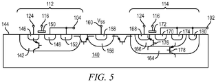
- FIG. 5 shows a cross sectional view of transistors 112 and 114 from FIG. 3 .
- Substrate 140 includes p-type semiconductor material, e.g., base silicon substrate doped with boron or gallium. Although the semiconductor structure is described for a p-type substrate, an n-type substrate, in a device or method which does not form part of the claimed invention, would have a similar structure with opposite type of semiconductor material for the substrate and semiconductor regions and opposite voltages.
- a deep n-well 142 is formed in surface 144 of substrate 140 by doping with n-type material, e.g., ion implantation of phosphorus or arsenic.
- P-region 146 is formed in n-well 142 as the drain of transistor 112 coupled to node 124.
- P-region 148 is formed in n-well 142 as the source of transistor 112 coupled to terminal 104.
- Gate structure 150 overlies the p-channel between p-region 146 and p-region 148 and is coupled to node 116.
- a vertical parasitic pnp is formed between p-region 146, n-well 142, and p-substrate 140.
- N-region 152 is formed in n-well 142 for good ohmic contact to terminal 104 and local potential V HIGH in order for transistor 112 to sustain high voltages and exhibit a low impedance RDSON.
- n-well 156 is formed in surface 144 of substrate 140 by doping with n-type material.
- N-region 158 is formed in n-well 156 for good ohmic contact to terminal 160 operating at V SS , e.g., ground potential.
- N-well 156 coupled to V SS represents other devices in the vicinity of charge pump cell 100.
- a lateral parasitic npn is formed between n-well 142, p-substrate 140, and n-well 156.
- a deep n-well 164 is formed in surface 144 of substrate 140 by doping with n-type material, e.g., ion implantation of phosphorus or arsenic.
- a local p-well 166 is formed within n-well 164 by doping with p-type material, e.g., ion implantation of boron or gallium.
- N-region 168 is formed in p-well 166 as the drain of transistor 114 coupled to node 124.
- N-region 170 is formed in p-well 166 as the source of transistor 114 coupled to terminal 102 and V LOW .
- Gate structure 172 overlies the n-channel between n-region 168 and n-region 170 and is coupled to node 116.
- P-region 174 is formed in p-well 166 for good ohmic contact to terminal 102 and V LOW in order for transistor 114 to sustain high voltages and exhibit a low impedance RDSON.
- a lateral parasitic npn is formed between n-well 156, p-substrate 140, and n-well 164.
- a vertical parasitic npn 176 is formed between n-region 168, p-well 166, and n-well 164.
- a vertical parasitic pnp 178 is formed between p-well 166, n-well 164, and p-substrate 140.
- n-well 164 is coupled to a local potential for the cell, i.e., terminal 102 and V LOW , as shown in FIGs. 3 and 5 . More specifically, n-region 180 is formed in n-well 164 for good ohmic contact, and terminal 102 and V LOW is coupled to n-region 180 and n-well 164. Note that p-well 166 is also coupled to terminal 102 and V LOW . Accordingly, the p-n (base and emitter) of vertical parasitic transistor 178 are shorted together by the common coupling to terminal 102 and V LOW , which disables operation of the parasitic transistor.
- the parasitic pnp structure 178 cannot become forward biased by charges injected from CLK and nCLK into p-well 166, n-well 164, and substrate 140 because n-well 164 and p-well 166 are both coupled to common terminal 102 and V LOW , which imposes a common local minimum potential to n-well 164 and p-well 166 (base-emitter junction potential of parasitic pnp structure 178 maintained at zero).
- parasitic pnp 178 or other parasitic pnp or npn structures in n-well 164 do not turn on due to common local potential at n-well 164 and p-well 166, internal latch-up is not triggered by the injection of carriers from the clock signal coupling through capacitors 110 and 118, substrate bounce, or other spurious voltages.
- Transistors 120 and 122 have a similar construction and arrangement as transistors 112 and 114 with the n-well and p-well of transistor 122 commonly coupled to terminal 102 and V LOW .
- a key feature is that n-well 164 and p-well 166 (regions of opposite conductivity type) are shorted to V LOW to prevent latch-up of charge pump cell 100. Accordingly, the p-n (base and emitter) of vertical parasitic transistor like 178 for transistor 122 are shorted together by the common coupling to terminal 102 and V LOW , which disables operation of the parasitic transistor.
- the parasitic pnp structure cannot become forward biased by charges injected from CLK and nCLK into the p-well, n-well, and substrate because the n-well and p-well for transistor 122 are both coupled to terminal 102 and V LOW , which imposes a common local potential to the n-well and p-well. Since the parasitic pnp or npn structures in the n-well do not turn on due to common local potential at the n-well and p-well of transistor 122, internal latch-up is not triggered by the injection of carriers from the clock signal coupling through capacitors 110 and 118, substrate bounce, or other spurious voltages.
- the well associated with V HIGH in one cell operates at the same potential as the well associated with V LOW of the next cell.
- Transistors are merged into a well region having a common potential. That is, transistors 112 and 120 are merged into the same physical n-well 142 within a cell, and transistors 114 and 122 are merged into the same physical n-well 164/p-well 166 within the same cell. Furthermore, transistors 112 and 120 associated with one cell are merged into the same physical well as transistors 114 and 122 associated with an adjacent cell due to the common potential, i.e., V HIGH of the one cell connected to V LOW of the adjacent cell. That is, n-well 142 of cell 100a are the same physical region as n-well 164 of cell 100b.
- the merging of wells within a cell and between cells provides for a higher density layout.
- the semiconductor structure described above including a substrate and first well region (n-well) formed in a substrate and second well region (p-well) formed in the first well region with the first and second well regions coupled to a common terminal to receive a local potential, is applicable to other types of electronic circuits.
- a key feature known from documents US 2010/0283533 A1 and EP 0 836 268 A1 is to maintain the p-n (base and emitter) of one or more parasitic transistors shorted together by common coupling to a local minimum potential to disable operation of the parasitic transistors. That is, n-well 164 and p-well 166 (regions of opposite conductivity type) are shorted to V LOW to prevent latch-up of charge pump cell 100.
- the parasitic pnp structure cannot become forward biased due to charges injected into the p-well, n-well, and substrate. Since the parasitic pnp or npn structures in the n-well do not turn on, latch-up is not triggered by the injection of carriers from charge injection, substrate bounce, or other spurious voltages.
Landscapes
- Engineering & Computer Science (AREA)
- Power Engineering (AREA)
- Semiconductor Integrated Circuits (AREA)
- Metal-Oxide And Bipolar Metal-Oxide Semiconductor Integrated Circuits (AREA)
- Dc-Dc Converters (AREA)
Description
- The present invention relates in general to semiconductor devices and, more particularly, to a semiconductor device comprising cascaded charge pump cells and to a method of making such a semiconductor device.
- Semiconductor devices are commonly found in modern electronic products. Semiconductor devices vary in the number and density of electrical components. Discrete semiconductor devices generally contain one type of electrical component, e.g., light emitting diode (LED), small signal transistor, resistor, capacitor, inductor, and power metal oxide semiconductor field effect transistor (MOSFET). Integrated semiconductor devices typically contain hundreds to millions of electrical components. Examples of integrated semiconductor devices include microcontrollers, microprocessors, application specific integrated circuits (ASICs), and other specific functional circuits.
- Semiconductor devices perform a wide range of functions such as signal processing, high-speed calculations, transmitting and receiving electromagnetic signals, controlling electronic devices, transforming sunlight to electricity, creating visual projections for television displays, and changing voltage levels. Semiconductor devices are found in the fields of entertainment, communications, power conversion, mechanical control, networks, computers, and consumer products. Semiconductor devices are also found in military applications, aviation, automotive, industrial controllers, and office equipment.
- A charge pump circuit is an example of a specific functional circuit that can be implemented on a substrate in a semiconductor die. The charge pump circuit receives an input voltage and then provides a different output voltage, either higher or lower than the input voltage. A charge pump circuit may contain a number of cells cascaded together with a voltage level shift per cell. The overall level shift of the output voltage is determined by the number of cells in the charge pump circuit, each providing a voltage level shift.
FIG. 1 illustrates a conventional dual bucketcharge pump cell 10 including dual cross-coupled metal oxide semiconductor (MOS) inverters receiving capacitive-coupled complementary clock signals. Theinput terminal 12 ofcharge pump cell 10 receives voltage VLOW whileterminal 14 provides cell output voltage VHIGH. Terminal 12 is coupled to a charge pump input voltage orterminal 14 of the preceding cell.Terminal 14 is coupled toterminal 12 of the next cell or provides the charge pump output voltage.Terminals charge pump cell 10 receive complementary clock signals CLK and nCLK of opposite phase. The clock signal CLK is coupled throughcapacitor 20 to the common gates of p-channel metal oxide semiconductor (PMOS)transistor 22 and n-channel metal oxide semiconductor (NMOS)transistor 24 atnode 26. The clock signal nCLK is coupled throughcapacitor 28 to the common gates ofPMOS transistor 30 andNMOS transistor 32 atnode 34. The sources oftransistors terminal 14. The drains oftransistors node 34, and the drains oftransistors node 26. The sources oftransistors terminal 12 and VLOW. - For a p-type substrate, a "high or higher voltage" generally refers to a positive voltage less than or equal to the maximum positive operating potential and greater than a "low or lower voltage", and the "low or lower voltage" generally refers to a positive voltage greater than or equal to the minimum operating potential (ground) and less than the "high or higher voltage." An n-type substrate would have opposite voltages. A voltage VLOW, e.g., zero volts or other power supply potential, is applied to
terminal 12. In cascaded charge pump cells, VHIGH from a previous cell is applied toterminal 12 as VLOW. Assume CLK is a high voltage, say +3 to +5 VDC, and nCLK is a low voltage, e.g., zero volts. Whencharge pump cell 10 is starting up, VLOW may be higher than VHIGH, which in turn is higher than or equal to Vsubstrate. The high CLK switchesNMOS transistor 24 to a conductive state (VGS24 greater than threshold VTH of the transistor) and rendersPMOS transistor 22 non-conductive (VGS22 not less than VTH).Capacitor 20 stores charge from the high CLK to increase the voltage atnode 26. The low nCLK switchesPMOS transistor 30 to a conductive state (VGS30 less than VTH) and rendersNMOS transistor 32 non-conductive (VGS32 not greater than VTH). The conductive state oftransistor 30 transfers the higher voltage atnode 26 directly through the source-drain conduction path oftransistor 30 toterminal 14 and causes VHIGH to increase toward the level of the clock signal, e.g., abs(CLK - nCLK) = 3 VDC. The conductive state oftransistor 24 dischargesnode 34 andcapacitor 28 toward voltage VLOW. - In the opposite phase of the clock signal, a high nCLK
renders PMOS transistor 30 non-conductive (VGS3O not less than VTH) and switchesNMOS transistor 32 to a conductive state (VGS32 greater than threshold VTH).Capacitor 28 stores charge from the high nCLK to increase the voltage atnode 34. The low CLK switchesPMOS transistor 22 to a conductive state (VGS22 less than VTH) and rendersNMOS transistor 24 non-conductive (VGS24 not greater than VTH). The conductive state oftransistor 22 transfers the higher voltage atnode 34 directly through the source-drain conduction path oftransistor 22 toterminal 14 and causes VHIGH to increase toward the level of the clock signal, e.g., +3 VDC. The conductive state oftransistor 32 dischargesnode 26 andcapacitor 20 toward voltage VLOW. The process repeats each clock cycle as the cross-coupled inverter pairs 22-24 and 30-32 alternatingly charge anddischarge capacitors node 26 or fromnode 34 toterminal 14. The discharge ofcapacitors transistors resets nodes - In steady state, VHIGH has a value of the clock signal, e.g., abs(CLK - nCLK) = 3 VDC. Accordingly,
charge pump cell 10 has increased the voltage from VLOW = 0 VDC to VHIGH = +3 VDC. Note thatcharge pump cell 10 is floating so for even higher voltages, multiple stages ofcharge pump cell 10 can be cascaded together withterminal 14 of the previous cell coupled toterminal 12 of the next cell. For example, the first cell increases VHIGH1 = VLOW1 + voltage level of the clock signal, i.e., VHIGH1 = 0 + 3. In the second cell, VLOW2 = VHIGH1, and VHIGH2 = VLOW2 + voltage level of the clock signal, i.e., VHIGH2 = 3 + 3 = +6 VDC. Additional cells can be added to the charge pump circuit to achieve practically any voltage necessary for the application, e.g., VHIGH of 10th cell = +30 VDC. -
Charge pump cell 10 is subject to internal latch-up, particularly during initial cycles of the clock signal. Latch-up inhibits normal operation of the charge pump circuit. In some cases, the internal latch-up can be traced to an activation of various vertical and lateral parasitic pnpn or npnp structures intransistors -
FIG. 2 shows a cross sectional view oftransistors FIG. 1 .Substrate 40 includes p-type semiconductor material, e.g., base silicon substrate doped with boron or gallium. A deep n-well 42 is formed insurface 44 ofsubstrate 40 by doping with n-type material, e.g., ion implantation of phosphorus or arsenic. P-region 46 is formed in n-well 42 as the drain oftransistor 22 coupled tonode 34. P-region 48 is formed in n-well 42 as the source oftransistor 22 coupled toterminal 14.Gate structure 50 overlies the p-channel between p-region 46 and p-region 48 and is coupled tonode 26. A vertical parasitic pnp is formed between p-region 46, n-well 42, and p-substrate 40. N-region 52 is formed in n-well 42 for good ohmic contact toterminal 14 and VHIGH in order fortransistor 22 to sustain high voltages and exhibit low drain-source resistance in the conductive state (RDSON). In a similar manner, n-well 56 is formed insurface 44 ofsubstrate 40 by doping with n-type material. N-region 58 is formed in n-well 56 for good ohmic contact toterminal 60 operating at VSS, e.g., ground potential. N-well 56 coupled to VSS represents other devices in the vicinity ofcharge pump cell 10. A lateral parasitic npn is formed between n-well 42, p-substrate 40, and n-well 56. - A deep n-
well 64 is formed insurface 44 ofsubstrate 40 by doping with n-type material, e.g., ion implantation of phosphorus or arsenic. N-well 64 is typically floating. A local p-well 66 is formed within n-well 64 by doping with p-type material, e.g., ion implantation of boron or gallium. N-region 68 is formed in p-well 66 as the drain oftransistor 24 coupled tonode 34. N-region 70 is formed in p-well 66 as the source oftransistor 24 coupled toterminal 12 and VLOW. Gate structure 72 overlies the n-channel between n-region 68 and n-region 70 and is coupled tonode 26. P-region 74 is formed in p-well 66 for good ohmic contact toterminal 12 and VLOW in order fortransistor 24 to sustain high voltages and exhibit a low impedance RDSON. A lateral parasitic npn is formed between n-well 56, p-substrate 40, and n-well 64. A verticalparasitic npn 76 is formed between n-region 68, p-well 66, and n-well 64. A verticalparasitic pnp 78 is formed between p-well 66, n-well 64, and p-substrate 40. - One of the potential causes of internal latch-up is the combination of parasitic pnp and npn structures and floating regions within the device, e.g.,
parasitic npn 76,parasitic pnp 78, and floating n-well 64. At start-up, there are no high voltages withincharge pump cell 10, although VLOW may be higher than VHIGH, and VHIGH is higher or equal to Vsubstrate, which is a factor that increases the occurrence of latch-up. Recall that n-well 42 is coupled to local VHIGH and p-well 66 is coupled to local VLOW with respect to chargepump cell 10 with n-well 64 floating. The initial low value of VHIGH creates a possibility for internal latch-up of the charge pump cell by forward biasing of one or more parasitic pnp and npn structures.Charge pump cell 10 receives voltages from CLK and nCLK throughcapacitors substrate 40, which can forward bias and activateparasitic npn 76 andparasitic pnp 78, or other parasitic npn and pnp structures. The combination of two or more parasitic pnp or npn structures activated by accumulation of the injected charges latches the conductive state of the parasitic pnp and npn structures like 76-78 and shorts n-region 68 to n-well 64 or p-well 66 tosubstrate 40. Alternatively, latch-up can be triggered by the parasitic pnp or npn structures and resistivity ofsubstrate 40. The injection of carriers from the clock signal coupling throughcapacitors charge pump cell 10 inhibits normal operation and can increase power consumption. The power drain is problematic in portable battery applications and can potentially damage the circuit by excessive power dissipation.US 2010/283533 A1 discloses a charge pump circuit. Each n-channel device is fabricated in a deep n-well formed in a p-substrate. A p-well is formed within the deep n-well. The drain regions are connected to the potential received by the first stage or to the output of another stage. An n-well is continually being switched to a node being discharged so that the n-well is boosted.
EP 0 836 268 A1 discloses a charge pump with a plurality of stages connected in series and discloses that for an efficient biasing of a bulk electrodes of the MOSFETs of the charge pump stages, two conflicting requirements must be taken into account. Firstly, the bias voltage of the bulk electrode should be sufficiently high to limit the body effect. Secondly, the voltage of the bulk electrode must always be lower or at most equal to the voltage of the source electrodes to prevent forward biasing of the source/bulk junction. - It is therefore the object of the present invention to provide an improved semiconductor device comprising two charge pump cells and a corresponding method of making a semiconductor device.
- This object is solved by the subject matter of the claims.
-
-
FIG. 1 illustrates a conventional charge pump cell with dual cross-coupled MOS inverters receiving capacitive-coupled complementary clock signals; -
FIG. 2 illustrates a cross-sectional view of a PMOS transistor and NMOS transistor in the charge pump cell ofFIG. 1 disposed in part in a floating n-well; -
FIG. 3 illustrates a charge pump cell with dual cross-coupled MOS inverters with the n-well containing the NMOS transistors coupled to a local potential; -
FIG. 4 illustrates a plurality of cascaded charge pump cells; and -
FIG. 5 illustrates a cross-sectional view of a PMOS transistor and NMOS transistor in the charge pump cell with the n-well coupled to a local potential. - The present invention is described in one or more embodiments in the following description with reference to the figures, in which like numerals represent the same or similar elements. While the invention is described in terms of the best mode for achieving the invention's objectives, it will be appreciated by those skilled in the art that it is intended to cover alternatives, modifications, and equivalents as may be included within the scope of the invention as defined by the appended claims and their equivalents as supported by the following disclosure and drawings.
-
FIG. 3 illustrates a dual bucketcharge pump cell 100 that can be implemented on a substrate in a semiconductor die. The charge pump circuit receives an input voltage and then provides a different output voltage, either higher or lower than the input voltage.Charge pump cell 100 includes dual cross-coupled MOS inverters receiving capacitive-coupled complementary clock signals of opposite phase. Theinput terminal 102 ofcharge pump cell 100 receives voltage VLOW whileterminal 104 provides cell output voltage VHIGH. Terminals 106 and 108 ofcharge pump cell 100 receive complementary clock signals CLK and nCLK. The clock signal CLK is coupled throughcapacitor 110 to the common gates ofPMOS transistor 112 andNMOS transistor 114 atnode 116. The clock signal nCLK is coupled throughcapacitor 118 to the common gates ofPMOS transistor 120 andNMOS transistor 122 atnode 124. The sources oftransistors terminal 104. The drains oftransistors node 124, and the drains oftransistors node 116. The sources oftransistors terminal 102 and VLOW. - For a p-type substrate as claimed, a "high or higher voltage" generally refers to a positive voltage less than or equal to the maximum positive operating potential and greater than a "low or lower voltage", and the "low or lower voltage" generally refers to a positive voltage greater than or equal to the minimum operating potential (ground) and less than the "high or higher voltage." A voltage VLOW, e.g., zero volts or other power supply potential, is applied to
terminal 102. In cascaded charge pump cells, VHIGH from a previous cell is applied toterminal 102 as VLOW. Assume CLK is a high voltage, say +3 to +5 VDC, and nCLK is a low voltage, e.g., zero volts. The high CLKswitches NMOS transistor 114 to a conductive state (VGS114 greater than threshold VTH of the transistor) and rendersPMOS transistor 112 non-conductive (VGS112 not less than VTH).Capacitor 110 stores charge from the high CLK to increase the voltage atnode 116. The low nCLK switchesPMOS transistor 120 to a conductive state (VGS120 less than VTH) and rendersNMOS transistor 122 non-conductive (VGS122 not greater than VTH). The conductive state oftransistor 120 transfers the higher voltage atnode 116 directly through the source-drain conduction path oftransistor 120 toterminal 104 and causes VHIGH to increase toward the level of the clock signal, e.g., abs(CLK - nCLK) = 3 VDC. The conductive state oftransistor 114discharges node 124 andcapacitor 118 toward voltage VLOW. - In the opposite phase of the clock signal, a high nCLK renders
PMOS transistor 120 non-conductive (VGS120 not less than VTH) and switchesNMOS transistor 122 to a conductive state (VGS122 greater than threshold VTH).Capacitor 118 stores charge from the high nCLK to increase the voltage atnode 124. The low CLK switchesPMOS transistor 112 to a conductive state (VGS112 less than VTH) and rendersNMOS transistor 114 non-conductive (VGS114 not greater than VTH). The conductive state oftransistor 112 transfers the higher voltage atnode 124 directly through the source-drain conduction path oftransistor 112 toterminal 104 and causes VHIGH to increase toward the level of the clock signal, e.g., +3 VDC. The conductive state oftransistor 122discharges node 116 andcapacitor 110 toward voltage VLOW. The process repeats each clock cycle as the cross-coupled inverter pairs 112-114 and 120-122 alternatingly charge and dischargecapacitors node 116 or fromnode 124 toterminal 104. The discharge ofcapacitors transistors resets nodes - In steady state, the local potential VHIGH has a value of the clock signal, e.g., abs(CLK - nCLK) = 3 VDC. Accordingly,
charge pump cell 100 has increased the voltage from VLOW = 0 VDC to VHIGH = +3 VDC. The charge pump circuit contains a number of cells, at least two according to the claimed invention, cascaded together with a voltage level shift per cell, as shown inFIG. 4 . The VHIGH of one cell is coupled to VLOW of the next cell. For example,terminal 102 ofcharge pump cell 100a receives a charge pump input voltage VIN = 0 VDC.Terminal 104 ofcharge pump cell 100a is coupled toterminal 102 ofcharge pump cell 100b.Terminal 104 ofcharge pump cell 100b is coupled toterminal 102 ofcharge pump cell 100c, or the next cell in the chain.Terminal 104 ofcharge pump cell 100c provides the charge pump output voltage VOUT. A primary clock signal atterminal 128 is buffered byamplifier 130 andinverter 132 to provide complementary CLK and nCLK to chargepump cells 100a-100c. The CLK and nCLK are coupled throughcapacitors pump cell 110a. The CLK and nCLK are coupled throughcapacitors pump cell 110b. The CLK and nCLK are coupled throughcapacitors pump cell 110c.Capacitor 134 is coupled betweenterminal 104 ofcharge pump cell 100c and terminal 136 operating at ground potential to provide filtering of the charge pump output voltage VOUT. -
Charge pump cell 100a increases VHIGH100a = VIN + voltage level of the clock signal, i.e., VHIGH100a = 0 + 3. With VHIGH of one cell coupled to VLOW of the next cell, VLOW100b = VHIGH100a, and UHIGH100b = VLOW100b + voltage level of the clock signal, i.e., VHIGH100b = 3 + 3 = +6 VDC incharge pump cell 100b. Additional cells, e.g.,charge pump cell 100c, can be added to the charge pump circuit to achieve practically any voltage necessary for the application. The overall level shift of the output voltage is determined by the number of cells in the charge pump circuit, each providing a voltage level shift. In one embodiment, VOUT can reach +90 VDC for control of mechanical devices. -
FIG. 5 shows a cross sectional view oftransistors FIG. 3 .Substrate 140 includes p-type semiconductor material, e.g., base silicon substrate doped with boron or gallium. Although the semiconductor structure is described for a p-type substrate, an n-type substrate, in a device or method which does not form part of the claimed invention, would have a similar structure with opposite type of semiconductor material for the substrate and semiconductor regions and opposite voltages. A deep n-well 142 is formed insurface 144 ofsubstrate 140 by doping with n-type material, e.g., ion implantation of phosphorus or arsenic. P-region 146 is formed in n-well 142 as the drain oftransistor 112 coupled tonode 124. P-region 148 is formed in n-well 142 as the source oftransistor 112 coupled toterminal 104.Gate structure 150 overlies the p-channel between p-region 146 and p-region 148 and is coupled tonode 116. A vertical parasitic pnp is formed between p-region 146, n-well 142, and p-substrate 140. N-region 152 is formed in n-well 142 for good ohmic contact toterminal 104 and local potential VHIGH in order fortransistor 112 to sustain high voltages and exhibit a low impedance RDSON. In a similar manner, n-well 156 is formed insurface 144 ofsubstrate 140 by doping with n-type material. N-region 158 is formed in n-well 156 for good ohmic contact to terminal 160 operating at VSS, e.g., ground potential. N-well 156 coupled to VSS represents other devices in the vicinity ofcharge pump cell 100. A lateral parasitic npn is formed between n-well 142, p-substrate 140, and n-well 156. - A deep n-well 164 is formed in
surface 144 ofsubstrate 140 by doping with n-type material, e.g., ion implantation of phosphorus or arsenic. A local p-well 166 is formed within n-well 164 by doping with p-type material, e.g., ion implantation of boron or gallium. N-region 168 is formed in p-well 166 as the drain oftransistor 114 coupled tonode 124. N-region 170 is formed in p-well 166 as the source oftransistor 114 coupled toterminal 102 and VLOW. Gate structure 172 overlies the n-channel between n-region 168 and n-region 170 and is coupled tonode 116. P-region 174 is formed in p-well 166 for good ohmic contact toterminal 102 and VLOW in order fortransistor 114 to sustain high voltages and exhibit a low impedance RDSON. A lateral parasitic npn is formed between n-well 156, p-substrate 140, and n-well 164. A verticalparasitic npn 176 is formed between n-region 168, p-well 166, and n-well 164. A verticalparasitic pnp 178 is formed between p-well 166, n-well 164, and p-substrate 140. - To resolve internal latch-up of
charge pump cell 100, particularly during initial cycles of the clock signal, n-well 164 is coupled to a local potential for the cell, i.e., terminal 102 and VLOW, as shown inFIGs. 3 and5 . More specifically, n-region 180 is formed in n-well 164 for good ohmic contact, andterminal 102 and VLOW is coupled to n-region 180 and n-well 164. Note that p-well 166 is also coupled toterminal 102 and VLOW. Accordingly, the p-n (base and emitter) of verticalparasitic transistor 178 are shorted together by the common coupling toterminal 102 and VLOW, which disables operation of the parasitic transistor. Theparasitic pnp structure 178 cannot become forward biased by charges injected from CLK and nCLK into p-well 166, n-well 164, andsubstrate 140 because n-well 164 and p-well 166 are both coupled tocommon terminal 102 and VLOW, which imposes a common local minimum potential to n-well 164 and p-well 166 (base-emitter junction potential ofparasitic pnp structure 178 maintained at zero). Sinceparasitic pnp 178 or other parasitic pnp or npn structures in n-well 164 do not turn on due to common local potential at n-well 164 and p-well 166, internal latch-up is not triggered by the injection of carriers from the clock signal coupling throughcapacitors -
Transistors transistors transistor 122 commonly coupled toterminal 102 and VLOW. A key feature is that n-well 164 and p-well 166 (regions of opposite conductivity type) are shorted to VLOW to prevent latch-up ofcharge pump cell 100. Accordingly, the p-n (base and emitter) of vertical parasitic transistor like 178 fortransistor 122 are shorted together by the common coupling toterminal 102 and VLOW, which disables operation of the parasitic transistor. The parasitic pnp structure cannot become forward biased by charges injected from CLK and nCLK into the p-well, n-well, and substrate because the n-well and p-well fortransistor 122 are both coupled toterminal 102 and VLOW, which imposes a common local potential to the n-well and p-well. Since the parasitic pnp or npn structures in the n-well do not turn on due to common local potential at the n-well and p-well oftransistor 122, internal latch-up is not triggered by the injection of carriers from the clock signal coupling throughcapacitors - In cascaded charge pump cells, as shown in
FIG. 4 , the well associated with VHIGH in one cell operates at the same potential as the well associated with VLOW of the next cell. Transistors are merged into a well region having a common potential. That is,transistors transistors transistors transistors cell 100a are the same physical region as n-well 164 ofcell 100b. The merging of wells within a cell and between cells provides for a higher density layout. - The semiconductor structure described above, including a substrate and first well region (n-well) formed in a substrate and second well region (p-well) formed in the first well region with the first and second well regions coupled to a common terminal to receive a local potential, is applicable to other types of electronic circuits. A key feature known from documents
US 2010/0283533 A1 andEP 0 836 268 A1 is to maintain the p-n (base and emitter) of one or more parasitic transistors shorted together by common coupling to a local minimum potential to disable operation of the parasitic transistors. That is, n-well 164 and p-well 166 (regions of opposite conductivity type) are shorted to VLOW to prevent latch-up ofcharge pump cell 100. The parasitic pnp structure cannot become forward biased due to charges injected into the p-well, n-well, and substrate. Since the parasitic pnp or npn structures in the n-well do not turn on, latch-up is not triggered by the injection of carriers from charge injection, substrate bounce, or other spurious voltages. - While one or more embodiments of the present invention have been illustrated in detail, the skilled artisan will appreciate that modifications and adaptations to those embodiments may be made without departing from the scope of the present invention as set forth in the following claims.
Claims (2)
- A semiconductor device comprising a first charge pump cell (100a) and a second charge pump cell (100b) cascaded together with an output of the first charge pump cell (100a) being coupled to an input of the second charge pump cell (100b), the semiconductor device comprising:a p-type substrate (140);each of the first (100a) and second (100b) charge pump cell comprising:a voltage input terminal (102);
a first well region (164) formed in the substrate and coupled to the voltage input terminal, wherein the first well region is doped with n-type material;
a second well region (166) formed within the first well region and coupled to the first well region and the voltage input terminal, wherein the second well region is doped with p-type material;
a first transistor (114) formed in the second well region (166), wherein the first transistor is an n-channel metal-oxide-semiconductor, NMOS, transistor, wherein a conduction region (170) of the first transistor is formed in the second well region as a source of the first transistor, and wherein the conduction region (170) of the first transistor is doped with n-type material and coupled to the voltage input terminal (102), the first well region and the second well region;
a second transistor (122) formed in the second well region (166), wherein the second transistor is an NMOS transistor, wherein a conduction region of the second transistor is formed in the second well region as a source of the second transistor, and wherein the conduction region of the second transistor is doped with n-type material and coupled to the voltage input terminal (102);
a third well region (142) formed in the substrate, wherein the third well region is doped with n-type material;
a third transistor (112) formed in the third well region (142), wherein the third transistor is a p-channel metal-oxide-semiconductor, PMOS, transistor, wherein a conduction region (148) of the third transistor is formed in the third well region as a source of the third transistor, and wherein the conduction region (148) of the third transistor is doped with p-type material;
a fourth transistor (120) formed in the third well region (142), wherein the fourth transistor is a PMOS transistor, wherein a conduction region of the fourth transistor is formed in the third well region as a source of the fourth transistor, and wherein the conduction region of the fourth transistor is doped with p-type material;
a voltage output terminal (104) coupled to the conduction region (148) of the third transistor (112) and to the conduction region of the fourth transistor (120);
a first clock terminal (106) coupled through a first capacitor (110) to a first node (116), the first node being coupled to the gate of the first transistor (114), to the gate of the third transistor (112), to the drain of the second transistor (122) and to the drain of the fourth transistor (120); and
a second clock terminal (108) coupled through a second capacitor (118) to a second node (124), the second node being coupled to the gate of the second transistor (122), to the gate of the fourth transistor (120), to the drain of the first transistor (114) and to the drain of the third transistor (112);
characterised in that:
in each of the first (100a) and second (100b) charge pump cells, the third well region (142) is coupled to the voltage output terminal (104), and the third well region (142) of the first charge pump cell (100a) is the same physical region as the first well region (164) of the second charge pump cell (100b). - A method of making a semiconductor device comprising a first charge pump cell (100a) and a second charge pump cell (100b) cascaded together with an output of the first charge pump cell (100a) being coupled to an input of the second charge pump cell (100b), the method comprising:providing a p-type substrate (140); and, for each of the first (100a) and second (100b) charge pump cells:forming a first well region (164) in the substrate, wherein the first well region is doped with n-type material;forming a second well region (166) within the first well region, wherein the second well region is doped with p-type material;forming a first transistor (114) in the second well region (166), wherein the first transistor is an n-channel metal-oxide-semiconductor, NMOS, transistor, wherein a conduction region (170) of the first transistor is formed in the second well region as a source of the first transistor, and wherein the conduction region (170) of the first transistor is doped with n-type material and coupled to a voltage input terminal (102), the first well region and the second well region;forming a second transistor (122) in the second well region (166), wherein the second transistor is an NMOS transistor, wherein a conduction region of the second transistor is formed in the second well region as a source of the second transistor, and wherein the conduction region of the second transistor is doped with n-type material and coupled to the voltage input terminal (102);forming a third well region (142) in the substrate, wherein the third well region is doped with n-type material;forming a third transistor (112) in the third well region (142), wherein the third transistor is a p-channel metal-oxide-semiconductor, PMOS, transistor, wherein a conduction region (148) of the third transistor is formed in the third well region as a source of the third transistor, wherein the conduction region (148) of the third transistor is doped with p-type material, and wherein the conduction region (148) of the third transistor (112) is coupled to a voltage output terminal (104); andforming a fourth transistor (120) in the third well region (142), wherein the fourth transistor is a PMOS transistor, wherein a conduction region of the fourth transistor is formed in the third well region as a source of the fourth transistor, and wherein the conduction region of the fourth transistor is doped with p-type material, and wherein the conduction region of the fourth transistor is coupled to the voltage output terminal (104);wherein, in each of the first (100a) and second (100b) charge pump cells, a first node (116) is coupled to the gate of the first transistor (114), to the gate of the third transistor (112), to the drain of the second transistor (122) and to the drain of the fourth transistor (120), the first node (116) being coupled to a first clock terminal (106) through a first capacitor (110), andwherein, in each of the first (100a) and second (100b) charge pump cells, a second node (124) is coupled to the gate of the second transistor (122), to the gate of the fourth transistor (120), to the drain of the first transistor (114) and to the drain of the third transistor (112), the second node (124) being coupled to a second clock terminal (108) through a second capacitor (118);characterised in that:
in each of the first (100a) and second (100b) charge pump cells, the third well region (142) is coupled to the voltage output terminal (104), and the third well region (142) of the first charge pump cell (100a) is the same physical region as the first well region (164) of the second charge pump cell (100b).
Applications Claiming Priority (3)
| Application Number | Priority Date | Filing Date | Title |
|---|---|---|---|
| US201261715185P | 2012-10-17 | 2012-10-17 | |
| US14/027,043 US9379103B2 (en) | 2012-10-17 | 2013-09-13 | Semiconductor device and method of preventing latch-up in a charge pump circuit |
| PCT/US2013/063026 WO2014062381A2 (en) | 2012-10-17 | 2013-10-02 | Semiconductor device and method of preventing latch-up in a charge pump circuit |
Publications (3)
| Publication Number | Publication Date |
|---|---|
| EP2909860A2 EP2909860A2 (en) | 2015-08-26 |
| EP2909860A4 EP2909860A4 (en) | 2015-10-14 |
| EP2909860B1 true EP2909860B1 (en) | 2018-07-18 |
Family
ID=50474614
Family Applications (1)
| Application Number | Title | Priority Date | Filing Date |
|---|---|---|---|
| EP13848087.6A Active EP2909860B1 (en) | 2012-10-17 | 2013-10-02 | Semiconductor device and method of preventing latch-up in a charge pump circuit |
Country Status (5)
| Country | Link |
|---|---|
| US (1) | US9379103B2 (en) |
| EP (1) | EP2909860B1 (en) |
| KR (1) | KR101815742B1 (en) |
| CN (1) | CN104769717B (en) |
| WO (1) | WO2014062381A2 (en) |
Families Citing this family (13)
| Publication number | Priority date | Publication date | Assignee | Title |
|---|---|---|---|---|
| DE102012202927B4 (en) * | 2012-02-27 | 2021-06-10 | Osram Gmbh | LIGHT SOURCE WITH LED CHIP AND LUMINOUS LAYER |
| JP6031954B2 (en) * | 2012-11-14 | 2016-11-24 | ソニー株式会社 | LIGHT EMITTING ELEMENT, DISPLAY DEVICE, AND ELECTRONIC DEVICE |
| KR102143520B1 (en) | 2014-09-17 | 2020-08-11 | 삼성전자 주식회사 | Pumping capacitor |
| US9491151B2 (en) * | 2015-01-07 | 2016-11-08 | Ememory Technology Inc. | Memory apparatus, charge pump circuit and voltage pumping method thereof |
| US20170162557A1 (en) * | 2015-12-03 | 2017-06-08 | Globalfoundries Inc. | Trench based charge pump device |
| EP3570422B1 (en) * | 2018-05-17 | 2021-01-13 | ams AG | Charge pump circuit arrangement |
| CN108550573B (en) * | 2018-05-29 | 2021-02-02 | 南京矽力微电子技术有限公司 | Electrostatic protection device and manufacturing method thereof |
| CN109037336A (en) * | 2018-06-19 | 2018-12-18 | 上海艾为电子技术股份有限公司 | Nmos device and chip including nmos device |
| US10892652B2 (en) | 2018-12-12 | 2021-01-12 | Semtech Corporation | Adaptive ping method for wireless charging system with wide charge distance |
| US10826389B1 (en) * | 2019-05-28 | 2020-11-03 | Samsung Electronics Co., Ltd. | Charge pump device and image sensor including the same |
| CN110676323B (en) * | 2019-09-17 | 2023-04-28 | 长江存储科技有限责任公司 | NMOS transistor and its forming method, charge pump circuit |
| TWI747790B (en) * | 2021-05-12 | 2021-11-21 | 友達光電股份有限公司 | Level shifter |
| US20250373234A1 (en) * | 2024-05-31 | 2025-12-04 | Nexperia B.V. | Cross-coupled latch charge pump as well as a method of operating such a cross-coupled latch charge pump |
Family Cites Families (12)
| Publication number | Priority date | Publication date | Assignee | Title |
|---|---|---|---|---|
| JP2771729B2 (en) | 1992-04-16 | 1998-07-02 | 三菱電機株式会社 | Charge pump circuit |
| US5475335A (en) | 1994-04-01 | 1995-12-12 | National Semiconductor Corporation | High voltage cascaded charge pump |
| US5734290A (en) | 1996-03-15 | 1998-03-31 | National Science Council Of R.O.C. | Charge pumping circuit having cascaded stages receiving two clock signals |
| US5828095A (en) | 1996-08-08 | 1998-10-27 | Micron Technology, Inc. | Charge pump |
| EP0836268B1 (en) | 1996-10-11 | 2002-02-06 | STMicroelectronics S.r.l. | Improved positive charge pump |
| TW486869B (en) * | 1999-12-27 | 2002-05-11 | Sanyo Electric Co | Voltage producing circuit and a display device provided with such voltage producing circuit |
| DE60207190D1 (en) | 2002-03-29 | 2005-12-15 | St Microelectronics Srl | Basic stage for charge pump circuit |
| TWI261406B (en) * | 2004-07-08 | 2006-09-01 | Analog Integrations Corp | Charge pump DC/DC converter with constant-frequency operation |
| FR2886783B1 (en) | 2005-06-03 | 2008-02-01 | Atmel Corp | HIGH PERFORMANCE BI-DIRECTIONAL LOAD PUMP |
| US7760010B2 (en) | 2007-10-30 | 2010-07-20 | International Business Machines Corporation | Switched-capacitor charge pumps |
| CN101662208B (en) * | 2008-08-26 | 2013-10-30 | 天利半导体(深圳)有限公司 | Charge pump circuit for realizing positive and negative high voltage |
| US20100283533A1 (en) | 2009-05-05 | 2010-11-11 | Numonyx Bv | Charge pump circuit and method |
-
2013
- 2013-09-13 US US14/027,043 patent/US9379103B2/en active Active
- 2013-10-02 EP EP13848087.6A patent/EP2909860B1/en active Active
- 2013-10-02 CN CN201380054122.2A patent/CN104769717B/en active Active
- 2013-10-02 WO PCT/US2013/063026 patent/WO2014062381A2/en not_active Ceased
- 2013-10-02 KR KR1020157009927A patent/KR101815742B1/en active Active
Non-Patent Citations (1)
| Title |
|---|
| None * |
Also Published As
| Publication number | Publication date |
|---|---|
| EP2909860A4 (en) | 2015-10-14 |
| WO2014062381A2 (en) | 2014-04-24 |
| US9379103B2 (en) | 2016-06-28 |
| US20140103415A1 (en) | 2014-04-17 |
| CN104769717A (en) | 2015-07-08 |
| CN104769717B (en) | 2019-01-04 |
| WO2014062381A3 (en) | 2014-06-19 |
| KR20150066539A (en) | 2015-06-16 |
| EP2909860A2 (en) | 2015-08-26 |
| KR101815742B1 (en) | 2018-01-05 |
Similar Documents
| Publication | Publication Date | Title |
|---|---|---|
| US9379103B2 (en) | Semiconductor device and method of preventing latch-up in a charge pump circuit | |
| US6429723B1 (en) | Integrated circuit with charge pump and method | |
| US9245888B2 (en) | Reverse polarity protection for n-substrate high-side switches | |
| US7345340B2 (en) | Semiconductor integrated circuit and a semiconductor device | |
| US7746147B2 (en) | Semiconductor device | |
| KR20100015887A (en) | Over-voltage tolerant pass-gate | |
| US5635745A (en) | Analog multiplexer cell for mixed digital and analog signal inputs | |
| US10453840B2 (en) | Semiconductor integrated circuit | |
| EP1155456A1 (en) | Improved esd diode structure | |
| US5714796A (en) | Integrated circuit device fabricated on semiconductor substrate blocking power supply lines from noise | |
| US9147695B2 (en) | Device with FD-SOI cell and insulated semiconductor contact region and related methods | |
| US20110260784A1 (en) | Decoupling circuit and semiconductor integrated circuit | |
| US20230238946A1 (en) | Level shifter | |
| US6570435B1 (en) | Integrated circuit with current limited charge pump and method | |
| US9154122B2 (en) | Latch up detection | |
| US5467048A (en) | Semiconductor device with two series-connected complementary misfets of same conduction type | |
| CN116504778B (en) | A high voltage ESD electrostatic layout structure | |
| US20200144814A1 (en) | Electrostatic discharge protection structure | |
| JP2978346B2 (en) | Input circuit of semiconductor integrated circuit device | |
| US7679427B2 (en) | Semiconductor device including a bias voltage generator | |
| CN117810945B (en) | Power supply reverse protection circuit, chip and electronic equipment | |
| JP2556684B2 (en) | Logic circuit | |
| US12633823B2 (en) | Multi-charge pump structure with related method | |
| CN116259624B (en) | A low-capacitance silicon-controlled rectifier | |
| CN112951820A (en) | Electrostatic protection structure and electrostatic protection circuit |
Legal Events
| Date | Code | Title | Description |
|---|---|---|---|
| PUAI | Public reference made under article 153(3) epc to a published international application that has entered the european phase |
Free format text: ORIGINAL CODE: 0009012 |
|
| 17P | Request for examination filed |
Effective date: 20150318 |
|
| AK | Designated contracting states |
Kind code of ref document: A2 Designated state(s): AL AT BE BG CH CY CZ DE DK EE ES FI FR GB GR HR HU IE IS IT LI LT LU LV MC MK MT NL NO PL PT RO RS SE SI SK SM TR |
|
| AX | Request for extension of the european patent |
Extension state: BA ME |
|
| RAP1 | Party data changed (applicant data changed or rights of an application transferred) |
Owner name: SEMTECH CORPORATION |
|
| REG | Reference to a national code |
Ref country code: DE Ref legal event code: R079 Ref document number: 602013040607 Country of ref document: DE Free format text: PREVIOUS MAIN CLASS: H01L0027060000 Ipc: H01L0027092000 |
|
| A4 | Supplementary search report drawn up and despatched |
Effective date: 20150915 |
|
| RIC1 | Information provided on ipc code assigned before grant |
Ipc: H01L 21/8238 20060101ALI20150909BHEP Ipc: H02M 3/07 20060101ALI20150909BHEP Ipc: H01L 27/092 20060101AFI20150909BHEP |
|
| DAX | Request for extension of the european patent (deleted) | ||
| 17Q | First examination report despatched |
Effective date: 20160704 |
|
| GRAP | Despatch of communication of intention to grant a patent |
Free format text: ORIGINAL CODE: EPIDOSNIGR1 |
|
| INTG | Intention to grant announced |
Effective date: 20180212 |
|
| RIN1 | Information on inventor provided before grant (corrected) |
Inventor name: CHEVROULET, MICHEL Inventor name: AEBISCHER, DANIEL |
|
| GRAS | Grant fee paid |
Free format text: ORIGINAL CODE: EPIDOSNIGR3 |
|
| GRAA | (expected) grant |
Free format text: ORIGINAL CODE: 0009210 |
|
| AK | Designated contracting states |
Kind code of ref document: B1 Designated state(s): AL AT BE BG CH CY CZ DE DK EE ES FI FR GB GR HR HU IE IS IT LI LT LU LV MC MK MT NL NO PL PT RO RS SE SI SK SM TR |
|
| REG | Reference to a national code |
Ref country code: GB Ref legal event code: FG4D |
|
| REG | Reference to a national code |
Ref country code: CH Ref legal event code: EP |
|
| REG | Reference to a national code |
Ref country code: IE Ref legal event code: FG4D |
|
| REG | Reference to a national code |
Ref country code: AT Ref legal event code: REF Ref document number: 1020266 Country of ref document: AT Kind code of ref document: T Effective date: 20180815 |
|
| REG | Reference to a national code |
Ref country code: DE Ref legal event code: R096 Ref document number: 602013040607 Country of ref document: DE |
|
| REG | Reference to a national code |
Ref country code: FR Ref legal event code: PLFP Year of fee payment: 6 |
|
| REG | Reference to a national code |
Ref country code: NL Ref legal event code: MP Effective date: 20180718 |
|
| REG | Reference to a national code |
Ref country code: LT Ref legal event code: MG4D |
|
| REG | Reference to a national code |
Ref country code: AT Ref legal event code: MK05 Ref document number: 1020266 Country of ref document: AT Kind code of ref document: T Effective date: 20180718 |
|
| PG25 | Lapsed in a contracting state [announced via postgrant information from national office to epo] |
Ref country code: NL Free format text: LAPSE BECAUSE OF FAILURE TO SUBMIT A TRANSLATION OF THE DESCRIPTION OR TO PAY THE FEE WITHIN THE PRESCRIBED TIME-LIMIT Effective date: 20180718 |
|
| PG25 | Lapsed in a contracting state [announced via postgrant information from national office to epo] |
Ref country code: FI Free format text: LAPSE BECAUSE OF FAILURE TO SUBMIT A TRANSLATION OF THE DESCRIPTION OR TO PAY THE FEE WITHIN THE PRESCRIBED TIME-LIMIT Effective date: 20180718 Ref country code: NO Free format text: LAPSE BECAUSE OF FAILURE TO SUBMIT A TRANSLATION OF THE DESCRIPTION OR TO PAY THE FEE WITHIN THE PRESCRIBED TIME-LIMIT Effective date: 20181018 Ref country code: GR Free format text: LAPSE BECAUSE OF FAILURE TO SUBMIT A TRANSLATION OF THE DESCRIPTION OR TO PAY THE FEE WITHIN THE PRESCRIBED TIME-LIMIT Effective date: 20181019 Ref country code: SE Free format text: LAPSE BECAUSE OF FAILURE TO SUBMIT A TRANSLATION OF THE DESCRIPTION OR TO PAY THE FEE WITHIN THE PRESCRIBED TIME-LIMIT Effective date: 20180718 Ref country code: RS Free format text: LAPSE BECAUSE OF FAILURE TO SUBMIT A TRANSLATION OF THE DESCRIPTION OR TO PAY THE FEE WITHIN THE PRESCRIBED TIME-LIMIT Effective date: 20180718 Ref country code: IS Free format text: LAPSE BECAUSE OF FAILURE TO SUBMIT A TRANSLATION OF THE DESCRIPTION OR TO PAY THE FEE WITHIN THE PRESCRIBED TIME-LIMIT Effective date: 20181118 Ref country code: LT Free format text: LAPSE BECAUSE OF FAILURE TO SUBMIT A TRANSLATION OF THE DESCRIPTION OR TO PAY THE FEE WITHIN THE PRESCRIBED TIME-LIMIT Effective date: 20180718 Ref country code: PL Free format text: LAPSE BECAUSE OF FAILURE TO SUBMIT A TRANSLATION OF THE DESCRIPTION OR TO PAY THE FEE WITHIN THE PRESCRIBED TIME-LIMIT Effective date: 20180718 Ref country code: AT Free format text: LAPSE BECAUSE OF FAILURE TO SUBMIT A TRANSLATION OF THE DESCRIPTION OR TO PAY THE FEE WITHIN THE PRESCRIBED TIME-LIMIT Effective date: 20180718 Ref country code: BG Free format text: LAPSE BECAUSE OF FAILURE TO SUBMIT A TRANSLATION OF THE DESCRIPTION OR TO PAY THE FEE WITHIN THE PRESCRIBED TIME-LIMIT Effective date: 20181018 |
|
| PG25 | Lapsed in a contracting state [announced via postgrant information from national office to epo] |
Ref country code: AL Free format text: LAPSE BECAUSE OF FAILURE TO SUBMIT A TRANSLATION OF THE DESCRIPTION OR TO PAY THE FEE WITHIN THE PRESCRIBED TIME-LIMIT Effective date: 20180718 Ref country code: LV Free format text: LAPSE BECAUSE OF FAILURE TO SUBMIT A TRANSLATION OF THE DESCRIPTION OR TO PAY THE FEE WITHIN THE PRESCRIBED TIME-LIMIT Effective date: 20180718 Ref country code: HR Free format text: LAPSE BECAUSE OF FAILURE TO SUBMIT A TRANSLATION OF THE DESCRIPTION OR TO PAY THE FEE WITHIN THE PRESCRIBED TIME-LIMIT Effective date: 20180718 |
|
| REG | Reference to a national code |
Ref country code: DE Ref legal event code: R097 Ref document number: 602013040607 Country of ref document: DE |
|
| PG25 | Lapsed in a contracting state [announced via postgrant information from national office to epo] |
Ref country code: EE Free format text: LAPSE BECAUSE OF FAILURE TO SUBMIT A TRANSLATION OF THE DESCRIPTION OR TO PAY THE FEE WITHIN THE PRESCRIBED TIME-LIMIT Effective date: 20180718 Ref country code: ES Free format text: LAPSE BECAUSE OF FAILURE TO SUBMIT A TRANSLATION OF THE DESCRIPTION OR TO PAY THE FEE WITHIN THE PRESCRIBED TIME-LIMIT Effective date: 20180718 Ref country code: CZ Free format text: LAPSE BECAUSE OF FAILURE TO SUBMIT A TRANSLATION OF THE DESCRIPTION OR TO PAY THE FEE WITHIN THE PRESCRIBED TIME-LIMIT Effective date: 20180718 Ref country code: IT Free format text: LAPSE BECAUSE OF FAILURE TO SUBMIT A TRANSLATION OF THE DESCRIPTION OR TO PAY THE FEE WITHIN THE PRESCRIBED TIME-LIMIT Effective date: 20180718 Ref country code: RO Free format text: LAPSE BECAUSE OF FAILURE TO SUBMIT A TRANSLATION OF THE DESCRIPTION OR TO PAY THE FEE WITHIN THE PRESCRIBED TIME-LIMIT Effective date: 20180718 |
|
| PLBE | No opposition filed within time limit |
Free format text: ORIGINAL CODE: 0009261 |
|
| STAA | Information on the status of an ep patent application or granted ep patent |
Free format text: STATUS: NO OPPOSITION FILED WITHIN TIME LIMIT |
|
| PG25 | Lapsed in a contracting state [announced via postgrant information from national office to epo] |
Ref country code: SM Free format text: LAPSE BECAUSE OF FAILURE TO SUBMIT A TRANSLATION OF THE DESCRIPTION OR TO PAY THE FEE WITHIN THE PRESCRIBED TIME-LIMIT Effective date: 20180718 Ref country code: DK Free format text: LAPSE BECAUSE OF FAILURE TO SUBMIT A TRANSLATION OF THE DESCRIPTION OR TO PAY THE FEE WITHIN THE PRESCRIBED TIME-LIMIT Effective date: 20180718 Ref country code: SK Free format text: LAPSE BECAUSE OF FAILURE TO SUBMIT A TRANSLATION OF THE DESCRIPTION OR TO PAY THE FEE WITHIN THE PRESCRIBED TIME-LIMIT Effective date: 20180718 |
|
| REG | Reference to a national code |
Ref country code: CH Ref legal event code: PL |
|
| 26N | No opposition filed |
Effective date: 20190423 |
|
| REG | Reference to a national code |
Ref country code: BE Ref legal event code: MM Effective date: 20181031 |
|
| PG25 | Lapsed in a contracting state [announced via postgrant information from national office to epo] |
Ref country code: LU Free format text: LAPSE BECAUSE OF NON-PAYMENT OF DUE FEES Effective date: 20181002 Ref country code: MC Free format text: LAPSE BECAUSE OF FAILURE TO SUBMIT A TRANSLATION OF THE DESCRIPTION OR TO PAY THE FEE WITHIN THE PRESCRIBED TIME-LIMIT Effective date: 20180718 |
|
| REG | Reference to a national code |
Ref country code: IE Ref legal event code: MM4A |
|
| PG25 | Lapsed in a contracting state [announced via postgrant information from national office to epo] |
Ref country code: SI Free format text: LAPSE BECAUSE OF FAILURE TO SUBMIT A TRANSLATION OF THE DESCRIPTION OR TO PAY THE FEE WITHIN THE PRESCRIBED TIME-LIMIT Effective date: 20180718 Ref country code: BE Free format text: LAPSE BECAUSE OF NON-PAYMENT OF DUE FEES Effective date: 20181031 Ref country code: LI Free format text: LAPSE BECAUSE OF NON-PAYMENT OF DUE FEES Effective date: 20181031 Ref country code: CH Free format text: LAPSE BECAUSE OF NON-PAYMENT OF DUE FEES Effective date: 20181031 |
|
| PG25 | Lapsed in a contracting state [announced via postgrant information from national office to epo] |
Ref country code: IE Free format text: LAPSE BECAUSE OF NON-PAYMENT OF DUE FEES Effective date: 20181002 |
|
| PG25 | Lapsed in a contracting state [announced via postgrant information from national office to epo] |
Ref country code: MT Free format text: LAPSE BECAUSE OF NON-PAYMENT OF DUE FEES Effective date: 20181002 |
|
| PG25 | Lapsed in a contracting state [announced via postgrant information from national office to epo] |
Ref country code: TR Free format text: LAPSE BECAUSE OF FAILURE TO SUBMIT A TRANSLATION OF THE DESCRIPTION OR TO PAY THE FEE WITHIN THE PRESCRIBED TIME-LIMIT Effective date: 20180718 |
|
| PG25 | Lapsed in a contracting state [announced via postgrant information from national office to epo] |
Ref country code: PT Free format text: LAPSE BECAUSE OF FAILURE TO SUBMIT A TRANSLATION OF THE DESCRIPTION OR TO PAY THE FEE WITHIN THE PRESCRIBED TIME-LIMIT Effective date: 20180718 |
|
| PG25 | Lapsed in a contracting state [announced via postgrant information from national office to epo] |
Ref country code: CY Free format text: LAPSE BECAUSE OF FAILURE TO SUBMIT A TRANSLATION OF THE DESCRIPTION OR TO PAY THE FEE WITHIN THE PRESCRIBED TIME-LIMIT Effective date: 20180718 Ref country code: MK Free format text: LAPSE BECAUSE OF NON-PAYMENT OF DUE FEES Effective date: 20180718 Ref country code: HU Free format text: LAPSE BECAUSE OF FAILURE TO SUBMIT A TRANSLATION OF THE DESCRIPTION OR TO PAY THE FEE WITHIN THE PRESCRIBED TIME-LIMIT; INVALID AB INITIO Effective date: 20131002 |
|
| P01 | Opt-out of the competence of the unified patent court (upc) registered |
Effective date: 20230607 |
|
| REG | Reference to a national code |
Ref country code: DE Ref legal event code: R079 Ref document number: 602013040607 Country of ref document: DE Free format text: PREVIOUS MAIN CLASS: H01L0027092000 Ipc: H10D0084850000 |
|
| PGFP | Annual fee paid to national office [announced via postgrant information from national office to epo] |
Ref country code: DE Payment date: 20251029 Year of fee payment: 13 |
|
| PGFP | Annual fee paid to national office [announced via postgrant information from national office to epo] |
Ref country code: GB Payment date: 20251027 Year of fee payment: 13 |
|
| PGFP | Annual fee paid to national office [announced via postgrant information from national office to epo] |
Ref country code: FR Payment date: 20251027 Year of fee payment: 13 |