EP2909601B1 - Method of increasing the debye length on a sensor surface within a sample solution and corresponding computer readable strorage medium - Google Patents
Method of increasing the debye length on a sensor surface within a sample solution and corresponding computer readable strorage medium Download PDFInfo
- Publication number
- EP2909601B1 EP2909601B1 EP13783780.3A EP13783780A EP2909601B1 EP 2909601 B1 EP2909601 B1 EP 2909601B1 EP 13783780 A EP13783780 A EP 13783780A EP 2909601 B1 EP2909601 B1 EP 2909601B1
- Authority
- EP
- European Patent Office
- Prior art keywords
- sensor
- electrode
- electrodes
- desalting
- sample
- Prior art date
- Legal status (The legal status is an assumption and is not a legal conclusion. Google has not performed a legal analysis and makes no representation as to the accuracy of the status listed.)
- Not-in-force
Links
Images


Classifications
-
- B—PERFORMING OPERATIONS; TRANSPORTING
- B03—SEPARATION OF SOLID MATERIALS USING LIQUIDS OR USING PNEUMATIC TABLES OR JIGS; MAGNETIC OR ELECTROSTATIC SEPARATION OF SOLID MATERIALS FROM SOLID MATERIALS OR FLUIDS; SEPARATION BY HIGH-VOLTAGE ELECTRIC FIELDS
- B03C—MAGNETIC OR ELECTROSTATIC SEPARATION OF SOLID MATERIALS FROM SOLID MATERIALS OR FLUIDS; SEPARATION BY HIGH-VOLTAGE ELECTRIC FIELDS
- B03C5/00—Separating dispersed particles from liquids by electrostatic effect
- B03C5/005—Dielectrophoresis, i.e. dielectric particles migrating towards the region of highest field strength
-
- G—PHYSICS
- G01—MEASURING; TESTING
- G01N—INVESTIGATING OR ANALYSING MATERIALS BY DETERMINING THEIR CHEMICAL OR PHYSICAL PROPERTIES
- G01N27/00—Investigating or analysing materials by the use of electric, electrochemical, or magnetic means
- G01N27/26—Investigating or analysing materials by the use of electric, electrochemical, or magnetic means by investigating electrochemical variables; by using electrolysis or electrophoresis
- G01N27/28—Electrolytic cell components
- G01N27/30—Electrodes, e.g. test electrodes; Half-cells
- G01N27/327—Biochemical electrodes, e.g. electrical or mechanical details for in vitro measurements
- G01N27/3275—Sensing specific biomolecules, e.g. nucleic acid strands, based on an electrode surface reaction
-
- G—PHYSICS
- G01—MEASURING; TESTING
- G01N—INVESTIGATING OR ANALYSING MATERIALS BY DETERMINING THEIR CHEMICAL OR PHYSICAL PROPERTIES
- G01N27/00—Investigating or analysing materials by the use of electric, electrochemical, or magnetic means
- G01N27/26—Investigating or analysing materials by the use of electric, electrochemical, or magnetic means by investigating electrochemical variables; by using electrolysis or electrophoresis
- G01N27/403—Cells and electrode assemblies
- G01N27/414—Ion-sensitive or chemical field-effect transistors, i.e. ISFETS or CHEMFETS
- G01N27/4145—Ion-sensitive or chemical field-effect transistors, i.e. ISFETS or CHEMFETS specially adapted for biomolecules, e.g. gate electrode with immobilised receptors
-
- G—PHYSICS
- G01—MEASURING; TESTING
- G01N—INVESTIGATING OR ANALYSING MATERIALS BY DETERMINING THEIR CHEMICAL OR PHYSICAL PROPERTIES
- G01N27/00—Investigating or analysing materials by the use of electric, electrochemical, or magnetic means
- G01N27/26—Investigating or analysing materials by the use of electric, electrochemical, or magnetic means by investigating electrochemical variables; by using electrolysis or electrophoresis
- G01N27/416—Systems
- G01N27/447—Systems using electrophoresis
- G01N27/44756—Apparatus specially adapted therefor
- G01N27/44791—Microapparatus
-
- G—PHYSICS
- G01—MEASURING; TESTING
- G01N—INVESTIGATING OR ANALYSING MATERIALS BY DETERMINING THEIR CHEMICAL OR PHYSICAL PROPERTIES
- G01N33/00—Investigating or analysing materials by specific methods not covered by groups G01N1/00 - G01N31/00
- G01N33/48—Biological material, e.g. blood, urine; Haemocytometers
- G01N33/50—Chemical analysis of biological material, e.g. blood, urine; Testing involving biospecific ligand binding methods; Immunological testing
- G01N33/53—Immunoassay; Biospecific binding assay; Materials therefor
- G01N33/543—Immunoassay; Biospecific binding assay; Materials therefor with an insoluble carrier for immobilising immunochemicals
- G01N33/54366—Apparatus specially adapted for solid-phase testing
- G01N33/54373—Apparatus specially adapted for solid-phase testing involving physiochemical end-point determination, e.g. wave-guides, FETS, gratings
- G01N33/5438—Electrodes
-
- B—PERFORMING OPERATIONS; TRANSPORTING
- B01—PHYSICAL OR CHEMICAL PROCESSES OR APPARATUS IN GENERAL
- B01L—CHEMICAL OR PHYSICAL LABORATORY APPARATUS FOR GENERAL USE
- B01L2200/00—Solutions for specific problems relating to chemical or physical laboratory apparatus
- B01L2200/06—Fluid handling related problems
- B01L2200/0631—Purification arrangements, e.g. solid phase extraction [SPE]
-
- B—PERFORMING OPERATIONS; TRANSPORTING
- B01—PHYSICAL OR CHEMICAL PROCESSES OR APPARATUS IN GENERAL
- B01L—CHEMICAL OR PHYSICAL LABORATORY APPARATUS FOR GENERAL USE
- B01L2200/00—Solutions for specific problems relating to chemical or physical laboratory apparatus
- B01L2200/06—Fluid handling related problems
- B01L2200/0694—Creating chemical gradients in a fluid
-
- B—PERFORMING OPERATIONS; TRANSPORTING
- B01—PHYSICAL OR CHEMICAL PROCESSES OR APPARATUS IN GENERAL
- B01L—CHEMICAL OR PHYSICAL LABORATORY APPARATUS FOR GENERAL USE
- B01L2200/00—Solutions for specific problems relating to chemical or physical laboratory apparatus
- B01L2200/10—Integrating sample preparation and analysis in single entity, e.g. lab-on-a-chip concept
-
- B—PERFORMING OPERATIONS; TRANSPORTING
- B01—PHYSICAL OR CHEMICAL PROCESSES OR APPARATUS IN GENERAL
- B01L—CHEMICAL OR PHYSICAL LABORATORY APPARATUS FOR GENERAL USE
- B01L2300/00—Additional constructional details
- B01L2300/06—Auxiliary integrated devices, integrated components
- B01L2300/0627—Sensor or part of a sensor is integrated
- B01L2300/0636—Integrated biosensor, microarrays
-
- B—PERFORMING OPERATIONS; TRANSPORTING
- B01—PHYSICAL OR CHEMICAL PROCESSES OR APPARATUS IN GENERAL
- B01L—CHEMICAL OR PHYSICAL LABORATORY APPARATUS FOR GENERAL USE
- B01L2400/00—Moving or stopping fluids
- B01L2400/04—Moving fluids with specific forces or mechanical means
- B01L2400/0403—Moving fluids with specific forces or mechanical means specific forces
- B01L2400/0415—Moving fluids with specific forces or mechanical means specific forces electrical forces, e.g. electrokinetic
-
- G—PHYSICS
- G01—MEASURING; TESTING
- G01N—INVESTIGATING OR ANALYSING MATERIALS BY DETERMINING THEIR CHEMICAL OR PHYSICAL PROPERTIES
- G01N27/00—Investigating or analysing materials by the use of electric, electrochemical, or magnetic means
- G01N27/26—Investigating or analysing materials by the use of electric, electrochemical, or magnetic means by investigating electrochemical variables; by using electrolysis or electrophoresis
- G01N27/403—Cells and electrode assemblies
- G01N27/414—Ion-sensitive or chemical field-effect transistors, i.e. ISFETS or CHEMFETS
- G01N27/4146—Ion-sensitive or chemical field-effect transistors, i.e. ISFETS or CHEMFETS involving nanosized elements, e.g. nanotubes, nanowires
Definitions
- the present disclosure relates to a method of increasing a Debye length and determining the presence of an analyte in a sample solution as defined by claim 1 as well as corresponding computer readable storage medium as defined in claim 16. Details of the method are specified in the dependent claims.
- Nanostructured sensors are widely used in the medical and chemical industries to measure the presence and/or concentration of a desired compound in a sample such as an analyte or other molecules. Nanostructured sensors typically require only a very small sample and are typically very sensitive. Common nanostructured sensors use electrical based detection such as, for example, field-effect transistors (FET). Typically, these sensors include semiconducting material located between two electrodes, whereby the semiconducting material is functionalized with a binding agent such as an antibody or aptamer. Binding a compound of interest or target molecule to the binding agent on the surface of the sensor induces electrical property changes through the semiconducting material and, thus, can be measured and correlated to the concentration of the compound within the sample.
- FET field-effect transistors
- Biosensors are commonly used to measure the concentration of an analyte such as an antibody, an antigen, etc. in a sample fluid such as serum, blood, or urine.
- Salt or ions build up at the biosensors and reduce sensitivity.
- Some example methods of desalting or deionizing samples utilize offline treatments with an ultrafiltration membrane. These methods suffer in that analytes that are present in low concentration may be lost during the filtration steps.
- Other example methods utilize desalting solutions such as dialysis, gel filtration columns, and on-chip membranes. These methods also suffer from drawbacks including potential loss of low-abundance proteins, increased cost, and increased complexity.
- the composite detection device comprises a membrane configured for desalting at least a portion of an analyte stream, and a nanostructure for detecting a bio-molecule or a bio-molecule interaction.
- the nanostructure and the membrane are arranged such that an analyte stream desalted at least in part by the membrane is detected by the nanostructure.
- a bio-sending detection system having the composite detection device and method of fabrication of the composite detection device are also provided.
- Document US 2011/198225 discloses a device and method of use thereof for desalting a solution.
- the method makes use of a device comprising microchannels, which are linked to conduits, whereby induction of an electric field in the conduit results in the formation of a space charge layer within the microchannel.
- the space charge layer provides an energy barrier for salt ions and generates an ion depletion zone proximal to the linkage region between the microchannel and the conduit.
- the method thus enables the removal of salt ions from the region proximal to the conduit and their accumulation in a region distant from the conduit, within the microchannel.
- Risveden et al disclose in "The region ion sensitive field effect transistor, a novel bioelectric nanosensor " a region ion sensitive field effect transistor (RISFET) nanosensor constructed on a sensor chip to measure glucose.
- the RISFET nanosensor includes two sensing electrodes that are spaced apart from each other and placed in a center of four outer metal plates. Ionic reaction products are selectively focused between the sensing electrodes using a region focusing electric field. In particular, a voltage drop is applied between a bottom capacitor plate and the four outer metal plates that causes a net positive charge on the bottom capacitor plate. The electric field created from the charged bottom capacitor plate is used to increase the number of ions within the sensing volume. Metal plates are so used to create an electric field that moves ions toward the center of the sensing electrodes.
- Ghallab Y H et al disclose in "A single CMOS chip for biocell trapping, levitation, detection and characterization " a chip that includes (1) an electric field generator, which is a quadrupole electrode configuration to produce a non-uniform electric field profile, and consequently a DEP force to levitate a cell that is desired to characterize, and (2) a sensing part, which is an array of differential electric field sensitive field effect transistors (DeFETs).
- the quadrupole configuration is used to trap and levitate a biocell at a central point where the array of DeFETs are located.
- the teaching is also focused on creating an electric field that concentrates or moves a biocell toward a sensor.
- US 2010/096268 discloses a device including a fluidic channel with electromotive electrodes, disposed at opposite ends of the channel for applying a potential along the fluid channel.
- a pair of sensing electrodes are disposed at two discrete locations along the length of the channel.
- the electromotive electrodes drive an analyte through the fluid channel and the analyte passes between the pair of sensing electrodes, which measures the changes in conductance of the electrolytic volume between them.
- WO 2012/138357 discloses a nanopore sensor including a membrane having a nanopore, which forms path between two fluidic reservoirs.
- the nanopore is used to measure electric potential for detection of species moving through the nanopore .
- Electrodes are provided to produce an electrophoretic force between the reservoirs for electrophoretically driving a fluidic solution (containing the species) through the nanopore from one reservoir to the other.
- nanostructured sensors e.g., biosensors
- electrical based detection such as, for example, field-effect transistors (FET)
- FET field-effect transistors
- Such nanostructured sensors operate by measuring a change in an electrical property that is modified upon binding or proximity of a molecule (e.g., a compound, an analyte, an antibody, an antigen, an aptamer and/or other substance).
- a molecule e.g., a compound, an analyte, an antibody, an antigen, an aptamer and/or other substance.
- a surface of the sensor is functionalized with a binding agent (e.g., a protein, a cell, a virus, a nucleic acid, an antigen, an antibody, a matrix protein, an enzyme, a coenzyme, a ligand, an aptamer, a receptor, etc.) to specifically bind with a particular molecule (e.g., analyte) known as an analyte of interest or target molecule. If an ionic concentration within the sample solution is low, the electrical properties of the surface of the sensor may change upon the binding of the analyte and, thus, the sensor can detect the analyte of interest.
- a binding agent e.g., a protein, a cell, a virus, a nucleic acid, an antigen, an antibody, a matrix protein, an enzyme, a coenzyme, a ligand, an aptamer, a receptor, etc.
- a particular molecule e.g., analy
- the analyte of interest has a net charge associated with it, and upon binding, the charge of the analyte modulates the charge density within a component of the sensor such as, for example, a semiconductive gate electrode of an FET.
- This modulation of charge density on the gate electrode of the FET is characterized by a change in one or more of a resistance, a current, a voltage, a capacitance, an impedance, etc.
- the gate electrode in the FET sensors includes a nanowire.
- a nanowire is a semiconductive structure that may include, for example, nanorod(s), nanotube(s), nanoribbon(s), etc. Furthermore, example nanowires have a large aspect ratio (e.g., length to width).
- nanowire sensors include semiconducting material located between the two electrodes (e.g., gate electrodes), whereby the semiconducting material is functionalized with a binding agent (e.g., antibody, aptamer, etc.).
- the gate electrodes are fabricated from materials including, for example, a semiconductive material such as, for example, silicon.
- the semiconductive material is doped to be an n-type semiconductor and, in some examples, the semiconductive material is doped to be a p-type semicondictor.
- nanowire sensors are able to advantageously measure concentrations of an analyte of interest in small samples.
- binding of an analyte of interest to the surface of the sensor induces electrical property changes through the semiconducting material, as described above.
- the electrical property is measured and correlated to the concentration of the analyte within the sample, and this detection can occur with very small sample sizes.
- nanowire sensors are sensitive and have low (atto-molar) detection limits in low ionic strength solutions.
- the sensitivity of nanowire sensors is limited by charge screening at high ionic strengths.
- these nanostructured sensors are affected by ionic charges (e.g., salt) in the sample fluid that can distort the detection operations.
- a Debye length is defined as the distance from a sensor surface at which ions (e.g., salt) in a solution effectively screen an electrical response induced by an analyte.
- Solutions with a high ionic strength have a small Debye length because the high number of ions negate charge influences at long distances.
- Samples are to be deionized (e.g., desalted) to maintain the low detection limits of analytes in physiological solutions. For example, an ionic strength of a physiological solution that is around 200 millimolar (mM) equates to a Debye length of around 1 nanometer (nm). Because a size of antibodies is about 5nm to about 10nm, the analyte binding events would be difficult to detect and may go undetected.
- mM millimolar
- An example apparatus which can be used for performing the method according to the invention, includes a substrate, a sensor coupled to the substrate where the sensor is to detect an analyte in a sample, and a first electrode to create an electric potential and reposition ions in the sample relative to a surface of the sensor.
- the sample is a raw sample and does not contain a buffer solution of low ionic concentration.
- the sensor comprises a field-effect transistor having a gate.
- the gate is functionalized with a binding agent to interact with the analyte.
- the gate comprises a nanostructure.
- the first electrode is to reposition ions in the sample closer to the gate of the field-effect transistor.
- the first electrode is substantially coplanar with the sensor on the substrate.
- the apparatus includes a second electrode disposed on the substrate.
- the sensor is located between the first electrode and the second electrode.
- the first electrode is to provide a positive electric voltage or a negative electric voltage and the second electrode is a ground electrode.
- the first electrode is to provide a positive electric voltage and the second electrode is to provide a negative electric voltage.
- both the first and second electrodes are to provide a positive electric voltage or both the first and second electrodes are to provide a negative electric voltage.
- the magnitude of the voltage differs between the first and second electrodes.
- the apparatus includes a third electrode and a fourth electrode disposed on the substrate.
- the first electrode, the second electrode, the third electrode and the fourth electrode are disposed on each of four sides around the sensor.
- the senor comprises a field-effect transistor having a source electrode, a drain electrode and a gate, and wherein the first electrode is disposed on at least one of the source electrode or the drain electrode.
- the method of increasing a Debye length and detecting the presence of an analyte in a sample solution includes introducing a sample into an apparatus comprising a sensor disposed on a substrate, the sensor configured to detect across the sensor a change in electrical property of a surface of the sensor that is changed upon binding of the analyte, and an electrode, separate from the sensor, disposed proximate to the sensor, applying an electric potential to the sample to redistribute ions in the sample relative to the sensor by moving the ions away from the sensor using the electric potential to increase a Debye length at the sensor surface and increase sensitivity of the sensor; and detecting, via the sensor, the presence of the analyte in the sample solution.
- detecting the presence of the analyte comprises measuring a change in at least one of a resistance, a current, a capacitance, an impedance or a voltage across the sensor. In some examples, the method further includes discontinuing the electric potential prior to detecting the presence of the analyte in the sample.
- FIG. 1 illustrates an example detection device or sensor 100 for measuring a concentration of a target molecule in a sample.
- the sensor 100 is a field effect transistor (FET) with a functionalized gate (e.g., semiconducting material).
- FET field effect transistor
- the sensor 100 may be, for example, a metal-oxide-semiconductor field effect transistor (MOSFET) or any other suitable sensor or biosensor for detecting and measuring the concentration of a target molecule.
- MOSFET metal-oxide-semiconductor field effect transistor
- the sensor 100 is disposed on a substrate 102 and includes a source electrode 104, a drain electrode 106 and a gate 108.
- the substrate 102 may comprise, for example, one or more of silicon oxide, titanium oxide, acryl resin, epoxy resin or polyimide.
- the gate 108 is functionalized (e.g., coated and/or doped) with a binding agent 110, which is adapted to react with a target molecule (e.g., an analyte of interest).
- a sample is placed in contact with the sensor.
- a drop of the sample may be placed on the sensor, the sensor may be disposed in a flow channel containing the sample and/or the sensor may otherwise be in fluid communication with a sample.
- the binding agent 110 As the target molecule in the sample interacts (e.g., binds, connects, reacts) with the binding agent 110, the charge density on the gate 108 is altered. As a result, one or more of a current, a voltage and/or a resistance across the gate 108 between the source electrode 104 and the drain electrode 106 may be measured. This change in electrical property across the gate 108 is correlated with the presence and/or concentration of the target molecule in the sample.
- the binding agent 110 has been enlarged to illustrate the concept of the gate 110. However, in practical applications, the binding agent 110 may be on the order of a few atoms or molecules and, thus, the ratio of the size of the binding agent 110 to other elements of the sensor 110 may differ.
- ions 112 (represented by "+” and "-") (e.g., salt ions) in the sample congregate near the surface (e.g., the gate 108) of the sensor 100.
- the ionic charges associated with the ions 112 decrease the sensitivity of the sensor 100 by interfering with the ability of the sensor 100 to detect the change in charge density caused by the binding of the target molecule and the binding agent 110. Separating the ions 112 from the surface of the sensor 100 a distance as little as on the order of nanometers may greatly increase the sensitivity of the sensor 100, thereby allowing the sensor 100 to obtain a more accurate reading of the target molecule.
- a Debye length is defined as the distance from a sensor surface at which ions in a solution screen (e.g., negate, interfere with) an electrical response induced by a target molecule.
- Example distances D1-D4 represent different Debye lengths associate various ion concentrations.
- ⁇ r represents the dielectric constant
- ⁇ 0 represents the permittivity of free space
- k B represents the Boltzmann constant
- T represents the temperature in Kelvin (K)
- N A represents Avogadro's constant
- e represents the elementary charge
- I represent ionic strength of the electrolyte.
- Debye length D1 may be 0.5 nanometers (nm), which occurs with very high ionic concentrations such as 100 millimolar (mM) solutions.
- the Debye length is 0.5nm, which is the distance at which the ions in the sample screen the electrical responses generated by a target molecule on the gate 108.
- the target molecule is about 5 nm, detection of the target molecule becomes extremely difficult.
- D2 represents a Debye length of 1.5nm occurring at an ionic concentration of 10mM
- D3 represents a Debye length of 4.6nm occurring at an ionic concentration of 1mM
- D4 represent a Debye length of 14.5nm occurring at an ionic concentration of 0.1mM.
- the ionic concentration of the sample at or near the sensor is decreased, thereby increasing the Debye length.
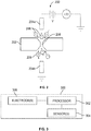
- FIG. 2 illustrates an example electrode device 200 used to move ions.
- the example device 200 may be used to deionize or desalt a sample to move ions away from a sensor surface.
- the device 200 of FIG. 2 may be used to manipulate the position of ions including, for example, moving ions through a membrane 202.
- a first electrode 204a and a second electrode 204b create an electric potential that drives ions 206 through a nanopore 208 in the membrane 202 toward the respective counter-electrode 204a, 204b.
- the first electrode 204a provides a positive charge (e.g., voltage) and the second electrode 204b provides a negative charge and, thus, the positively charged (+) ions 206 are attracted to the second electrode 204b and the negatively charged (-) ions 206 are attracted to the first electrode 204a.
- the first and second electrodes 204a, 204b are made of silver and silver chloride.
- other suitable material(s) may be used such as, for example, titanium, platinum, gold and/or any other suitable material.
- the example apparatus, systems and methods disclosed herein provide a fast, passive methodology of mitigating the desensitizing effects of salt ions in solution.
- the example apparatus, systems and methods disclosed utilize one or more localized electrodes (e.g., with DC potential) to attract salt ions away from the surface of a sensor for at least a period of time sufficient to ensure an accurate reading from the sensor.
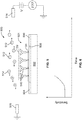
- FIG. 3 is a block diagram of an example desalting system 300.
- the example desalting system 300 includes a processor 302 communicatively coupled to one or more sensor(s) 304 and one or more electrode(s) 306.
- the sensors 304 may be, for example, nanowire sensors used to measure a concentration or a presence of an analyte of interest in a sample.
- the electrode(s) 306 are used to create an electric potential (e.g., an electrical field, a charge) near the sensor(s) 304 to attract or migrate disruptive salt ions away from the sensor(s) 304 and towards the electrode(s) 306.
- an electric potential e.g., an electrical field, a charge
- the type (e.g., DC, AC, DC+AC, etc.) and/or the strength (e.g., +1V, +2V, etc.) of the electric potential generated by the electrodes is varied.
- the frequency and/or timing of an AC electric field and/or super-imposed DC field is varied.
- FIGS. 4A and 4B show an example system or apparatus for desalting samples 400, which may be incorporated, for example, into the system 300 of FIG. 3 .
- a sensor 401 is used to measure the presence and/or concentration of an analyte of interest in a sample.
- the sensor 401 is a FET and is disposed on a substrate 402.
- the sensor 401 includes a source electrode 404, a drain electrode 406 and a gate 408, which is functionalized with a binding agent 410.
- sample is placed in contact with the surface of the sensor 401, and an analyte of interest in the sample interacts with the binding agent 410 to affect the charge density at the gate 408.
- a plurality of ions 412 are present in the sample and congregate around the surface of the sensor 401.
- a single electrode 414 e.g., a desalting electrode
- deionize e.g., desalt
- the desalting electrode 414 is disposed above or otherwise spaced apart from the sensor 401 and is to attract or repel the ions 412, depending on the charge created by the desalting electrode 414 and the charge of the ions 412.
- the desalting electrode 414 is disposed on the substrate 402 adjacent the sensor 401.
- the desalting electrode 414 is substantially coplanar with the source electrode 404, the drain electrode 406 and/or the gate 408.
- the desalting electrode 414 produces an electric potential
- the ions 412 are attracted and/or repelled to/by the desalting electrode 414, depending on the charge of the desalting electrode 414 and the charge of the ions 412.
- the Debye length is increased and, thus, the sensitivity of the sensor 401 is also increased.
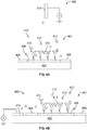
- FIG. 5 shows a side view of another example system or apparatus for desalting samples 500, which may be used by, for example, the system 300 of FIG. 3 .
- a sensor 501 is disposed on a substrate 502 and includes a source electrode 504, a drain electrode 506 and a gate 508, which is functionalized with a binding agent 510.
- a sample is placed in contact with the surface of the sensor 501, and an analyte of interest in the sample interacts with the binding agent 510 to affect the charge density at the gate 508.
- a plurality of ions 512 are present in the sample and congregate around the surface of the sensor 501.
- ions tend to screen or interfere with the electrical properties generated on the gate 508.
- a first desalting electrode 514 and a second desalting electrode 516 are provided to move the salt ions 512 away from the surface of the sensor 501.
- Application of an electric potential by, for example, a direct-current (DC) moves the ions away from the sensor 501 and towards the first and second desalting electrodes 514, 516. Moving the ions away from the sensor 500 increases the Debye length (e.g., from D1 to D2) and increases the sensitivity and detection capabilities of the sensor 501.
- DC direct-current
- the sample prior to desalting, may have a Debye length of D1, which may be smaller than the size of the binding agent 510 and/or target molecule.
- the ions screen electrical charges generated on the gate 508 and interfere with the sensitivity of the sensor 501.
- the negative (-) salt ions 512 are attracted to the first desalting electrode 514, and the positive (+) salt ions are attracted to the second desalting electrode 516 (or vice versa depending on the charges at the respective desalting electrodes 514, 516).
- the Debye length is increased to about D2 (e.g., about 20 nm), and the sensitivity of the sensor 501 is increased.
- the first and second desalting electrodes 514, 516 are silver and silver chloride electrodes.
- other suitable material(s) may be used such as, for example, titanium, platinum, gold and/or other suitable materials.
- the apparatus or system 500 includes specifically positioned electrodes 514, 516. Though two electrodes are shown in FIG. 5 , any other suitable number of electrodes may also be used such as, for example, one, three, four, ten, or more electrodes.
- the electrodes 514, 516 may be placed in particular locations and/or geometric configurations to optimize the movement of ions away from the sensor 501.
- the one or more of the electrodes are embedded on the same chip as the sensor 501 (i.e., coplanar).
- the electric potential is applied to the first and second desalting electrodes 514, 516 after the sample has been incubated. In such examples, if the analyte of interest were charged, the analyte of interest could be bound to the surface of the sensor 501 before being affected by the DC potential. Also, in some examples, the electric potential at the first and second desalting electrodes 514, 516 is turned or switched off prior to measuring the analyte of interest. In other examples, the electric potential is applied throughout the measuring the process.
- the electric potential causes the salt ions in solution to electrophoretically migrate towards the first and second counter-charged desalting electrodes 514, 516.
- ⁇ ep represents the electrophoretic mobility
- E represents the strength of the electric field.
- q is the elementary charge of a molecule (e.g., ionic charge)
- f is a frictional component (e.g., collisional component)
- ⁇ is the viscosity of solution
- r is the hydrodynamic radius of the ion (e.g., ionic radius).
- the viscosity for a sample may be about 1.27 megapascals (MPa) (assuming Stokes approximations), the electric field is about 100 V/m (1 volt (V) separated by about 1cm), the ionic charge of sodium is about 1.6x10 -19 , and the hydrodynamic radius of sodium is about 0.358nm.
- the resulting sodium ion velocity of this example is about 3.28 ⁇ m/s (which accounts for differences in the hydrodynamic radii of sodium ions).
- the viscosity is about 1.27MPa
- the electric field is about 500 V/m (5V separated by about 1cm)
- the ions include sodium ions having a radius of about 0.358nm and ionic charge of 1.6x10 -19 .
- the resulting ion velocity of this example is about 9.35 ⁇ m/s.
- the arrangement shown in FIG. 5 reduces non-specific binding to the surface of the sensor 501.
- q the elementary charge of the molecule
- E the strength of the electric field.
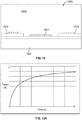
- FIG. 6 is a graph of the sensitivity of the sensor 501 over time. As shown, the sensitivity increases with time because as time lapses, more ions in the solution are moved away from the sensor 501 and toward the electric potentials generated at the first and second desalting electrodes 514, 516.
- FIG. 7 illustrates the example apparatus or system 500 of FIG. 5 after a period of time of operation when the salt ions 512 have been attracted to the first and second desalting electrodes 514, 516.
- the negative charged salt ions 512 have gathered around first desalting electrode 514 and the positively charged salt ions 512 have gathered around second electrode 516 and, thus, the negative (-) and positive (+) ions have been moved away from the surface of the sensor 501.
- FIG. 8 is another graph of the sensitivity of the sensor 501 over time. As shown, the sensitivity experiences a rate of decay over time, which may happen, for example, when the desalting electric potential is lost. The rate of decay depends on variable(s) such as, for example, a diffusion rate, and/or a concentration of ions driving the diffusion rate.
- D is a diffusion constant
- ⁇ ( r , t ) is the density of the diffusing material at location r and time t
- D ( ⁇ , r ) is the collective diffusion coefficient for density ⁇ at location r
- ⁇ represents the vector differential operator del.
- the diffusion equation describes the density dynamics in a material undergoing diffusion. The rate of diffusion is proportional to the concentration of ions in the solution and, therefore, an original concentration of ions may be estimated by measuring the rate of change of concentration.
- the examples disclosed herein also account for transport phenomena such as, for example, diffusion, which may occur when the electric potential is turned off prior or otherwise not continuous.
- a sodium ion, Na+ may have a diffusion rate in serum of about 11.5 ⁇ m 2 /s.
- One second of diffusion may move the ion about 7 ⁇ m.
- the example apparatus and systems disclosed herein can account for diffusion when determining the duration for which to operate or apply the electrical potential to sufficiently clear the surface of the sensor from ions to achieve the desired Debye length, the desired sensitivity of the sensor and the desired concentration reading.
- FIG. 9 illustrates another example system or apparatus for desalting samples 900, which may be used, for example, in the system 300 of FIG. 3 .
- a sensor 901 is an FET and is disposed on a substrate 902.
- the sensor 901 includes a source electrode 904, a drain electrode 906, and a gate 908, which has been functionalized with a binding agent 910.
- a sample is placed in contact with the surface of the sensor 901, and the analyte of interest interacts with the binding agent 910 on the gate 908.
- ions 912 congregate near the surface of the sensor 901 and may screen the electric response(s) generated at the gate 910.
- a first desalting electrode 914 and a second desalting electrode 916 are provided on the substrate 902 to move the ions 912 away from the surface of the gate 908.
- the first and second desalting electrodes 914, 916 are substantially coplanar with the source electrode 904, the drain electrode 906 and/or the gate 908.
- the first desalting electrode 914 is spaced from the source electrode 904 and the second desalting electrode 916 is spaced from the drain electrode 906.
- the first desalting electrode 914, the source electrode 904, the drain electrode 906 and the second desalting electrode 916 are in a linear arrangement with the gate 908.
- the electric potential created by the first and second desalting electrodes 914, 916 attracts the ions 912, moves the ions 912 in the sample away from the gate 908 and, thus, reduces the screening caused at the gate 908.
- FIGS. 10 and 11 show another example system or apparatus for desalting samples 1000, which may be incorporated, for example, into the system 300 of FIG. 3 .
- a sensor 1001 is disposed on a substrate 1002 and includes a source electrode 1004, a drain electrode 1006 and a gate 1008, which is functionalized with a binding agent.
- a first desalting electrode 1010 and a second desalting electrode 1012 are disposed on the substrate 1002 and are provided to move ions in a sample away from the surface of the gate 1008.
- the first and second desalting electrodes 1010, 1012 are substantially coplanar with the source electrode 1004, the drain electrode 1006 and/or the gate 1008.
- the source electrode 1004, the gate 1008 and the drain electrode 1006 are linearly aligned along an axis 1013.
- the first desalting electrode 1010 is disposed on a first side of the axis 1013
- the second desalting electrode 1012 is disposed on a second side of the axis 1013, opposite the first side.
- the first and second desalting electrodes 1010, 1012 are spaced apart from the axis 1013.
- the relative lengths of the first and second desalting electrodes 1010, 1012 and/or the respective distances of the first and second desalting electrodes 1010, 1012 from the gate 1008 affect the sensing behavior of the sensor 1001.
- smaller desalting electrodes placed further from the axis 1013 will increase the sensitivity of the sensor 1001 less than larger desalting electrodes placed closer to the axis 1013.
- positioning the desalting electrodes 1010, 1012 too close to the sensor 1001 may create an electric field that may cause dielectric breakdown of various materials in the sample. Therefore, the dimensions and parameters disclosed above may be adjusted to optimize the sensing behavior of the sensor 1001.
- the first desalting electrode 1010 has an electric potential represented by V 1
- the second desalting electrode 1012 has an electric potential represented by V 2
- the electric potential V 1 may be a positive or a negative voltage applied to the first desalting electrode 1010 (e.g., +1V, - IV, +0.25mV, -0.25mV, etc.).
- the second desalting electrode 1012 is grounded, and the electric potential V 2 of the second desalting electrode 1012 is substantially zero (0).
- V 1 is a positive voltage
- V 1 is a negative ions in the sample are attracted to the first desalting electrode 1010.
- V 1 is a negative voltage
- positively charged ions in the sample are attracted to the first desalting electrode 1010.
- V offset an offset voltage
- FIG. 12 shows the example apparatus or system 1000 shown in FIGS. 10 and 11 as used in a bulk sample supply system.
- a flow of sample 1014 is provided past or over the sensor 1001.
- the flow of sample 1014 may be provided in a flow channel (e.g., a microfluidic flow channel) having a sample that is to be tested.
- the first and second desalting electrodes 1010, 1012 are provided to move ions in the sample 1014 away from the surface of the sensor 1001.
- the first and second desalting electrodes 1010, 1012 are activated to move the ions away from the sensor 1001.
- the example sensor 1001 may be any sensor/electrode arrangement disclosed herein.
- any sensor/electrode arrangement described herein may be incorporated into a sample flow channel for testing a sample while the sample is flowing through the flow channel and in contact with the sensor and electrode arrangement.
- the sample is stationary on the sensor and electrode such as, for example, in a well.
- FIGS. 13A-E are graphs representing example relationships between different properties of the example sensor and electrode arrangements disclosed herein.
- FIG. 13A shows the current at the drain electrode (I drain ) (e.g., the drain electrode 1006) over time.
- the desalting electrodes are activated at time zero (0), and, as time increases, the current at the drain generally increases.
- the current at the drain is indicative of charge density cause by target molecules in the sample.
- the amount of current detected across the gate e.g., the gate 1008 also increases.
- the amount of current at the drain eventually levels or remains constant or near constant over time.
- the leveling of the drain current occurs because a potentially maximum amount of the ions in the sample have been removed from or moved away from the sensor.
- the desalting electrodes may attract a limited capacity of ions. Once the surfaces of the desalting electrodes are substantially covered by ions, additional ions in the sample remain dispensed in the sample.
- FIG. 13B is a graph showing the current generated at the desalting electrodes (I electrdoes ) versus time as averaged over different electrode voltages.
- the desalting electrodes are activated at time zero (0).
- the desalting electrodes When the desalting electrodes are initially activated, there is a high current at the desalting electrodes, which is the result of the ions rapidly moving toward the desalting electrodes.
- the current at the desalting electrodes decreases and generally levels (e.g., remains constant or near constant) over time. In some examples, the leveling occurs because movement of the ions has decreased and a potentially maximum amount of the ions have already been attracted to the desalting electrodes. In other examples, such as samples with high ionic concentrations, the desalting electrodes may attract a limited capacity of ions. Once the surfaces of the desalting electrodes are substantially covered by ions, additional ions in the sample remain dispensed in the sample.
- FIG. 13C is a graph showing the current generated at the desalting electrodes versus time as average over different ionic concentrations of the samples.
- the desalting electrodes are activated at time zero (0). As shown, when the electrodes are initially activated, there is a high current at the electrodes, which is the result of the ions rapidly moving toward the electrodes. Similar to the trend shown in FIG. 13B , as time passes, the current at the electrodes decreases and generally tapers off for the reasons noted above.
- FIG. 13D is a graph showing the current at the drain electrode (I drain ) relative to the voltage of the desalting electrode(s). As shown, as the voltage in the desalting electrodes is increased, the current at the drain (e.g., across the gate) also increases. As mentioned above, as the ions in the sample are moved away from the sensor, the change in charge density on the sensor is more easily detected and a current may flow from the source electrode to the drain electrode. Increasing the voltage of the desalting electrode(s), creates a higher electric field to more rapidly and effectively attract/repel ions in the sample.
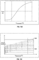
- FIG. 13E is a graph showing the amount of voltage needed to desalt different volumes of samples having different ionic concentrations to approximately 1% of their bulk concentration.
- the line 1300 represents a sample having a relatively high ionic concentration (e.g., 1000mM) and line 1302 represents a sample having a relatively low ionic concentration (e.g., .0001mM).
- the lines between line 1300 and 1302 represent sample with increasing ionic concentrations between that of 1300 and 1302.
- the samples having lower ionic concentrations e.g., line 1302
- the amount of samples that could be desalted is higher than the samples with higher ionic concentrations (e.g., line 1300).
- This example illustrates that samples with lower ionic concentrations can be desalted more readily and with lower electrode voltages than samples with higher ionic concentrations.
- FIG. 14 shows a side view of an example system or apparatus for desalting samples 1400, which may be incorporated, for example, into the system 300 of FIG. 3 .
- a sensor 1401 is disposed on a substrate 1402 between a first electrode 1404 and a second electrode 1406.
- the first and second electrodes 1404, 1406 provide an electric potential to move ions in a sample 1408 away from the surface of the sensor 1401.
- the height of the first and second electrodes 1404, 1406 relative to the height of the sensor 1401 has been increased.
- the first and second electrodes 1404, 1406 have more surface area to attract ions in the sample 1408. Thus, more ions can be attracted by the first and second electrodes 1404, 1406.
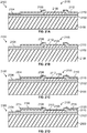
- FIG. 15A is an example top view of the apparatus or system shown in FIG. 14 .
- a well 1500 defined by the sensor 1401 and the first and second electrodes 1404, 1406 is substantially square shaped.
- the width W1 of the first and second electrodes 1404, 1406 is relatively narrower compared to the width W2 of the substrate 1402.
- FIG. 15B shows an alternative top view of apparatus or system of FIG. 14 , where the width W3 of the first and second electrodes 1404, 1406 is wider relative to W2 than the example shown in FIG. 15A .
- FIG. 15B shows an alternative top view of apparatus or system of FIG. 14 , where the width W3 of the first and second electrodes 1404, 1406 is wider relative to W2 than the example shown in FIG. 15A .
- a well 1502 defined by the sensor 1401 and the first and second electrodes 1404, 1406 is substantially rectangular.
- sample may travel between the first and second electrodes 1404, 1406 and over the surface of the sensor 1401.
- the relative surface area of the first and second electrodes 1404, 1406 is changed and, thus, may affect the sensing behavior of the sensor 1401. For example, wider and/or higher or deeper desalting electrodes may move a greater number of ions and increase the sensitivity of the sensor 1401.
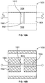
- FTG.16A is a side view of another example system or apparatus for desalting samples 1600 that may be incorporated, for example, into the system 300 of FIG. 3 .
- a sensor 1601 is disposed on a first substrate 1602 between a first electrode 1604 and a second electrode 1606.
- a second substrate 1608 is disposed on top of the first and second electrodes 1604, 1606 and, thus, a flow channel 1610 is formed by the second substrate 1608, the first and second electrodes 1604, 1606, the sensor 1601 and the first substrate 1602.
- the first and second electrodes 1604, 1606 provide an electric potential to move ions in a sample, flowing through the channel 1610, away from the surface of the sensor 1601.
- FIG. 1 similar to the example shown in FIG.
- the height of the first and second electrodes 1604, 1606 relative to the height of the sensor 1601 has been increased than shown in some prior examples.
- the first and second electrodes 1604, 1606 have more surface area to attract ions in the sample.
- FIG. 16B is a cross-sectional view of the sensor and electrode arrangement shown in FIG. 16A taken along the A-A line.
- the flow channel 1610 includes branches, and the sample fluid may enter through one or more of the sides and across the surface of the sensor 1601 between the first and second electrodes 1604, 1606.
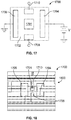
- FIG. 17 illustrates another system or apparatus for desalting samples 1700, which may be incorporated, for example, into the system 300 of FIG. 3 .
- a sensor 1701 is disposed on a substrate 1702 between a first electrode 1704, a second electrode 1706, a third electrode 1708 and a fourth electrode 1710.
- the first, second, third and fourth electrodes 1704-1710 are all desalting electrodes and provide electrical potential(s) to move ions away from the sensor 1701.
- the electrodes 1704-1710 may be paired together, such that one electrode provides a positive electric potential and the other electrode provides a negative electric potential.
- the first electrode 1704 and the third electrode 1708 may provide a positive electrical potential and the second electrode 1706 and the fourth electrode 1710 may provide a negative electrical potential.
- negative ions in the sample would migrate toward the positive electric potential created by the first electrode 1704 and the third electrode 1708.
- positively charged ions in the sample would migrate toward the negative electric potential created by the second electrode 1706 and the fourth electrode 1710.
- one of the pair of electrodes may provide a substantive potential (e.g., a positive or negative potential) and the other electrode may be a ground (e.g., provide substantially zero (0) potential).
- the first, second, third and fourth electrodes 1704-1710 are substantially coplanar with the sensor 1701 and arranged in a square pattern around the sensor 1701.
- the distance between each of the electrodes 1704-1710 and the sensor 1701 may be altered to change the sensing behavior of the sensor 1701, as disclosed herein.
- the first and second electrodes 1704, 1704 are relatively longer than the third and fourth electrodes 1708, 1710.
- more or fewer electrodes are provided on the substrate 1702 and may be configured in other arrangements.
- each electrode may have a unique dimension, all may have identical dimensions, and/or any combination of repeating and/or unique shape(s) and/or size(s).
- the first and second electrodes 1704, 1706 are desalting electrodes and the third and fourth electrodes 1708, 1710 are sensing electrodes for an additional device such as, for example, an impedance sensor.
- the third and fourth electrodes 1708, 1710 are used to measure the electrical resistance in the sample, which may be used to verify the desalting operation.
- FIG. 18 shows a portion of microchip sensor 1800 having the example system or apparatus 1700 shown in FIG. 17 , and which may be incorporated, for example, into the system 300 of FIG. 3 .
- the sensor 1701 and the electrodes 1704-1710 are disposed on the surface of the microchip 1800.
- a sample may be applied to the microchip 1800 and the sensor 1701 detects the concentration of a target molecule in the sample.
- one or more of the electrodes 1704-1710 function as desalting electrodes to move ions away from the sensor 1701.
- the electrodes 1704-1710 operate in pairs.
- FIG. 19 is an example system or apparatus for desalting samples 1900.
- the example arrangement 1900 may be incorporated, for example, into the system 300 of FIG. 3 .
- the example system or apparatus 1900 includes a chip 1902 on which sensors 1904a, 1904b, 1904c, 1904d (e.g., biosensor, nanowire sensors, FETs) and a plurality of electrodes 1906a, 1906b, 1906c, 1906d, 1906e, 1906f, 1906g, 1906h are disposed.
- the system or apparatus 1900 may include more or fewer electrodes.
- the example sensors 1904a-d detect biomolecules or biomolecular binding events.
- the example electrodes 1906a-h may be insulated such that a current does not flow through the solution.
- the sensors 1904a-d are substantially surrounded by the electrodes 1906a-h on the chip 1902.
- the electrodes 1906a-h are positioned away from and apart from the sensors 804a-d and create an electrical potential such that counter-charged ionic salt species in a sample migrate towards the electrodes 1906a-h and away from the sensors 1904a-d.
- the migration of the salt ions increases both the Debye length and the sensitivity of the sensors 1904a-d.
- the example system or apparatus 1900 shown allows the sample to be desalted (i.e., deionized) on the chip rather than an external process being needed.
- the electrodes 1906a-h also remove non-specifically bound proteins from the sensor surface.
- Many proteins in solutions maintain a net ionic charge and, therefore, the proteins may be attracted towards the electrodes 1906a-h. Because the specifically bound proteins are more strongly bound, the potential necessary to detach the proteins is higher than the potential necessary to detach non-specifically bound proteins. Thus, it is possible to minimize non-specific binding on a sensor surface.
- Other ions such as, for example, sodium, potassium, and chloride ions may also be directed towards the electrodes on the sensor surface, thereby locally desalting the sample and allowing for a low ionic content during sensor measurements.
- the number of electrodes may be varied.
- the shape and/or the geometry of one or more of the electrode(s) may be varied. Some examples may include electrodes in a ring shape, electrodes in an elliptical shape, two parallel lines of electrodes, intersecting lines of electrodes, an arc of electrodes, a single side of electrodes, and/or any other suitable pattern.
- one or more of the electrode(s) may be coplanar with the sensors and in other examples, the one or more of the electrode(s) may not be co-planar with one or more of the sensor(s).
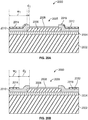
- FIGS. 20A and 20B show cross-sectional views of an example system or apparatus for desalting samples 2000 disposed on a substrate 2002, which may include, for example, a silicon chip, a microchip, etc.
- a substrate 2002 which may include, for example, a silicon chip, a microchip, etc.
- an insulator layer 2004 e.g., a layer of buried oxide, silicon dioxide
- a sensor 2005 such as, for example, an FET sensor, is disposed on the substrate 2002 and includes a gate 2006 (e.g., a TiN extended gate) that, in this example, includes an insulator layer 2008 (e.g., hafnium oxide (HfO 2 )).
- a gate 2006 e.g., a TiN extended gate
- an insulator layer 2008 e.g., hafnium oxide (HfO 2 )
- the gate 2006 is disposed between a first inter-layer dielectric insulator 2010 and a second inter-layer dielectric insulator 2012.
- a first electrode 2014 e.g., a desalting electrode
- a second electrode 2016 e.g., a desalting electrode
- the first and second electrodes 2014, 2016 may comprise any suitable electrode material(s) such as, for example, gold, platinum, silver, silver chloride, titanium and/or other suitable material(s).
- the first and second electrodes 2014, 2016 are layered onto the first and second inter-layer dielectric insulators 2010, 2012, respectively, and are separated a distance d 1 from the edge of the respective first and second inter-layer dielectric insulators 2010, 2012 and, thus, the edge of the gate 2006 of the sensor 2005.
- the first and second electrodes 2014, 2016 have a width or length of wi.
- the distances d 1 and w 1 may be varied to affect the sensing behavior of the sensor 2000. For example, as shown in FIG. 20B , the distance d 2 is greater than d 1 and the distance w 2 is smaller than the distance w 1 in FIG. 20A .
- FIGS. 21A-D show cross-sectional views of an example system or apparatus for desalting samples 2100, which may be, for example, an on-chip electrode sensor and electrode device.
- FIGS. 21A-D illustrate an example fabrication process of the example system or apparatus 2100.
- the example sensor 2100 includes a substrate 2101 which may be, for example, an FET sensing chip.
- the sensor 2100 also includes an insulator layer 2102, which may include, for example, a buried oxide.
- the example sensor 2100 includes a first electrode layer 2104, which may include, for example, gold.
- a sensor 2105 having a gate 2106 (e.g., a TiN extended gate) that is disposed on the first insulator layer 2102 is also included.
- a gate 2106 e.g., a TiN extended gate
- the gate 2106 is disposed between a first inter-layer dielectric insulator 2108 and a second inter-layer dielectric insulator 2110.
- an insulator layer 2112 is disposed over the gate 2106.
- the insulator layer 2112 may be, for example, HfO 2 .
- a portion of the insulator layer 2112 is removed by, for example, wet etching to expose the electrode layer 2104 as shown in FIG. 21B . Removal of a portion the insulator layer 2112 to expose at least a portion of the electrode layer 2104 assists in low temperature wire-bonding for coupling the desalting electrodes at the macroscopic level to, for example, a printed circuit board (PCB) and/or card reader.
- PCB printed circuit board
- FIG. 21C shows that a first electrode layer 2114 (e.g., a deionizing or desalting electrode) and a second electrode layer 2116 (e.g., a deionizing or desalting electrode) are deposited on the sensor 2105.
- the first and second inter-layer dielectric insulators 2108, 2110 insulate the desalting electrodes.
- the first and second electrode layers 2114, 2116 are platinum.
- the first and second electrode layers 2114, 2116 may comprise other suitable electrode material(s) such as, for example, gold, silver, silver chloride, titanium, etc.
- the desalting electrodes 2114, 2116 are included using a two-layer combination of a lift-off resist and a positive tone thin photoresist. In other examples, other methods of depositing the electrodes are used.
- the example system or apparatus, 2100 also includes a first oxide dielectric layer 2118 and a second oxide dielectric layer 2120, as shown in FIG. 21D .
- the dielectric layers 2118, 2120 include a layer of plasma-enhanced chemical vapor deposition (PECVD).
- PECVD plasma-enhanced chemical vapor deposition
- the first oxide dielectric layer 2118 is coupled to the first electrode 2114 and the second oxide dielectric layer 2120 is coupled to the second electrode 2116.
- portion(s) of the oxide dielectric layers 2118, 2120 may be removed and/or patterns formed therein via a subtractive processing such as, for example, photolithography, wet-etching, etc.
- portion(s) of the dielectric layers 2128, 2120 exposes the first and second desalting electrodes 2114, 2116 in the sensing region around the gate 2106.
- passivation occurs by use of the PECVD layers, which decreases the amount of surface area of the desalting electrodes 2114, 2116 in contact with the sample.
- FIGS. 22 and 23 are perspective views of an example system or apparatus for desalting samples 2200, which may be utilized, for example, by the system 300 of FIG. 3 .
- the examples shown in FIGS. 22 and 23 illustrate example passivated and exposed desalting electrode configurations.
- a sensor 2201 is disposed on a substrate 2202 between a first desalting electrode 2204, a second desalting electrode 2206, a first sensing electrode 2208 and a second sensing electrode 2210.
- the first and second sensing electrodes 2208, 2210 may be used to measure the voltage and/or impedance occurring in the sample.
- the first and second sending electrodes 2208, 2210 are desalting electrodes and are used to move ions away from the sensor 2201.
- the first and second desalting electrodes 2204, 2206 create an electric potential to move ions in the sample away from the surface of the sensor 2201.
- the length of the first and second desalting electrodes 2204, 2206 and the distance from the first and second desalting electrodes 2204, 2206 to the sensor 2200 affect the sensing behavior.
- a passivated configuration such as that shown in FIG. 22 , includes a first passivation layer 2212 that covers by, for example, coating, encapsulating, shielding, etc. the first desalting electrode 2204.
- the example also includes a second passivation layer 2214 that covers the second desalting electrode 2206.
- the first and second passivation layers 2212, 2214 shield specific areas, portions, or sections of the first and second desalting electrodes 2204, 2206 from exposure to electrochemical activity within the sample solution so that only a small region of the sensor 2201 is exposed.
- passivation is used to decrease the likelihood of a short circuit between the first and second desalting electrodes 2204, 2206.
- the first and second passivation layers 2212, 2214 are smaller and cover less of the first and second desalting electrodes 2204, 2206 than the example shown in FIG. 22 .
- the first and second desalting electrodes 2204, 2206 are substantially more exposed to the sample and, thus, more surface area of the first and second desalting electrodes 2204, 2206 is exposed to move ions away from the sensor 2201.
- one or more of the electrode(s) and/or the sensor(s) described herein may have a movable position that changes during and/or between application of electrical potentials.
- the strength and/or duration of electric fields may be varied.
- the type of electric field e.g., DC, AC, DC and AC, etc.
- the electrode material of one or more of the electrode(s) is varied.
- the frequency and/or timing of an AC field and/or super-imposed DC field is varied.
- one or more of the electrode(s) are embedded and/or coated with a dielectric to prevent (or accelerate) chemical reactions. The different multiple configurations and variants may be modified and/or combined in any suitable manner to optimize the electric fields.
- the sample solution of interest is a biological sample. In other examples, the solution of interest is a non-biological sample. In some examples, the sample solution includes blood, serum, plasma, and/or urine. In some examples, the biosensor detects proteins, antibodies, antigens, viruses, and/or nucleic acids. In other examples, the sensor detects a change in local pH, which, for example, is used in molecular (e.g., DNA) sensing.
- molecular e.g., DNA
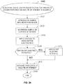
- Fig. 24 is a flowchart representative of example machine readable instructions for implementing the example desalting systems or apparatus 300, 400, 500, 900, 1000, 1400, 1600, 1700, 1900, 2000, 2100 and 2200 of FIGS. 3 , 4A , 4B , 5 , 7 , 9-12 and 14-23 .
- the machine readable instructions comprise a program for execution by a processor such as the processor 2512 shown in the example computer 2500 discussed below in connection with FIG. 25 .
- the program may be embodied in software stored on a tangible computer readable medium such as a CD-ROM, a floppy disk, a hard drive, a digital versatile disk (DVD), a Blu-ray disk, or a memory associated with the processor 2512, but the entire program and/or parts thereof could alternatively be executed by a device other than the processor 2512 and/or embodied in firmware or dedicated hardware.
- a tangible computer readable medium such as a CD-ROM, a floppy disk, a hard drive, a digital versatile disk (DVD), a Blu-ray disk, or a memory associated with the processor 2512, but the entire program and/or parts thereof could alternatively be executed by a device other than the processor 2512 and/or embodied in firmware or dedicated hardware.
- the example processes of FIG. 24 may be implemented using coded instructions (e.g., computer and/or machine readable instructions) stored on a tangible computer readable storage medium such as a hard disk drive, a flash memory, a read-only memory (ROM), a compact disk (CD), a digital versatile disk (DVD), a cache, a random-access memory (RAM) and/or any other storage device or storage disk in which information is stored for any duration (e.g., for extended time periods, permanently, for brief instances, for temporarily buffering, and/or for caching of the information).
- a tangible computer readable storage medium is expressly defined to include any type of computer readable storage device and/or storage disk and to exclude propagating signals and to exclude transmission media.
- tangible computer readable storage medium and “tangible machine readable storage medium” are used interchangeably. Additionally or alternatively, the example processes of FIG. 24 may be implemented using coded instructions (e.g., computer and/or machine readable instructions) stored on a non-transitory computer and/or machine readable medium such as a hard disk drive, a flash memory, a read-only memory, a compact disk, a digital versatile disk, a cache, a random-access memory and/or any other storage device or storage disk in which information is stored for any duration (e.g., for extended time periods, permanently, for brief instances, for temporarily buffering, and/or for caching of the information).
- a non-transitory computer readable medium is expressly defined to include any type of computer readable storage device and/or storage disk and to exclude propagating signals and to exclude transmission media.
- FIG. 24 An example method 2400 of increasing the Debye length and detecting the presence an analyte of interest in a sample is shown in FIG. 24 .
- the example method 2400 may be, for example, performed by the processor 302, the sensors 304 and/or the electrodes 306 shown in FIG. 3 .
- the processor 302 is communicatively coupled to the sensors 304 and the electrodes 306.
- the sensors 304 are used to measure the presence of an analyte of interest in a sample fluid.
- the processor 302 controls the electrodes 306 to create an electric potential and attract ions in the sample away from the sensors 304 and towards the electrodes 306.
- the example process 900 includes introducing a sample into a detection device (block 2402) that includes a sensor such as, for example, the example sensors 304, 401, 501, 901, 1001, 1401, 1601, 1701, 1904a-d, 2005, 2105 and/or 2201 disclosed above.
- the sample may be, for example, serum, blood, urine, etc.
- the sample may be manually loaded and/or, in some examples, automatically introduced to the detection device.
- the sample is introduced to the detection device via a flow channel such as, for example, the flow channel shown in FIGS. 12 , 16A and 16B .
- the sample is stationary on the sensor (e.g., in a well).
- the example process 2400 also includes incubating (block 2404). In some examples, the sample is incubated on a surface of a sensor (block 2404). In other examples, the example process 2400 continues without incubating the sample.
- the example process 2400 also includes applying an electric potential (block 2406) via desalting electrodes.
- the electric potential may be applied, for example, during incubation and/or after incubation.
- the electric potential is produced from the desalting electrodes 306, 414, 514, 516, 914, 916, 1010, 1012, 1404, 1406, 1604, 1606, 1704-1710, 1906a-h, 2014, 2016, 2114, 2116, 2204 and/or 2206 disclosed above.
- the application of an electric potential attracts ions in the sample to the counter-charged desalting electrodes and moves the ions away from the surface of the detection device or sensor.
- the example process 900 also includes determining whether to switch off or otherwise remove or discontinue the electric potential (block 2408).
- the electrical potential may continue and the detection device measures the presence of the analyte of interest (block 2410).
- the electric potential is stopped (block 2412) prior to measuring the presence of the analyte of interest (bock 2414).
- the analyte of interest is measured using a sensor such as, for example, the sensors 304, 401, 501, 901, 1001, 1401, 1601, 1701, 1904a-d, 2005, 2105 and/or 2201 disclosed above.
- the example process 2400 avoids eliminating the salt ions the bulk sample, unlike prior methods. Rather, with the example systems, apparatus and methods disclosed herein, the salt ions are repositioned. The Debye length at the sensor surface is increased due to the migration of the ions towards the electrodes.
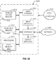
- FIG. 25 is a block diagram of an example processor platform 2500 capable of executing the instructions of FIG. 24 to implement the example desalting systems and apparatus 300, 400, 500, 900, 1000, 1400, 1600, 1700, 1900, 2000, 2100 and 2200 of FIGS. 3 , 4A , 4B , 5 , 7 , 9-12 and 14-23 .
- the processor platform 2500 can be, for example, a server, a personal computer, a mobile device (e.g., a cell phone, a smart phone, a tablet such as an iPadTM), a personal digital assistant (PDA), an Internet appliance, a DVD player, a CD player, a digital video recorder, a Blu-ray player or any other type of computing device.
- a mobile device e.g., a cell phone, a smart phone, a tablet such as an iPadTM
- PDA personal digital assistant
- an Internet appliance e.g., a DVD player, a CD player, a digital video recorder, a
- the processor platform 2500 of the illustrated example includes a processor 2512.
- the processor 2512 of the illustrated example is hardware.
- the processor 2512 can be implemented by one or more integrated circuits, logic circuits, microprocessors or controllers from any desired family or manufacturer.
- the processor 2512 of the illustrated example includes a local memory 2513 (e.g., a cache).
- the processor 2512 of the illustrated example is in communication with a main memory including a volatile memory 2514 and a non-volatile memory 2516 via a bus 2518.
- the volatile memory 2514 may be implemented by Synchronous Dynamic Random Access Memory (SDRAM), Dynamic Random Access Memory (DRAM), RAMBUS Dynamic Random Access Memory (RDRAM) and/or any other type of random access memory device.
- the non-volatile memory 2516 may be implemented by flash memory and/or any other desired type of memory device. Access to the main memory 2514, 2516 is controlled by a memory controller.
- the processor platform 2500 of the illustrated example also includes an interface circuit 2520.
- the interface circuit 2520 may be implemented by any type of interface standard, such as an Ethernet interface, a universal serial bus (USB), and/or a PCI express interface.
- one or more input devices 2522 are connected to the interface circuit 2520.
- the input device(s) 2522 permit(s) a user to enter data and commands into the processor 2512.
- the input device(s) can be implemented by, for example, an audio sensor, a microphone, a camera (still or video), a keyboard, a button, a mouse, a touchscreen, a track-pad, a trackball, isopoint and/or a voice recognition system.
- One or more output devices 2524 are also connected to the interface circuit 2520 of the illustrated example.
- the output devices 2524 can be implemented, for example, by display devices (e.g., a light emitting diode (LED), an organic light emitting diode (OLED), a liquid crystal display, a cathode ray tube display (CRT), a touchscreen, a tactile output device, a light emitting diode (LED), a printer and/or speakers).
- the interface circuit 2520 of the illustrated example thus, typically includes a graphics driver card, a graphics driver chip or a graphics driver processor.
- the interface circuit 2520 of the illustrated example also includes a communication device such as a transmitter, a receiver, a transceiver, a modem and/or network interface card to facilitate exchange of data with external machines (e.g., computing devices of any kind) via a network 2526 (e.g., an Ethernet connection, a digital subscriber line (DSL), a telephone line, coaxial cable, a cellular telephone system, etc.).
- a communication device such as a transmitter, a receiver, a transceiver, a modem and/or network interface card to facilitate exchange of data with external machines (e.g., computing devices of any kind) via a network 2526 (e.g., an Ethernet connection, a digital subscriber line (DSL), a telephone line, coaxial cable, a cellular telephone system, etc.).
- DSL digital subscriber line
- the processor platform 2500 of the illustrated example also includes one or more mass storage devices 2528 for storing software and/or data.
- mass storage devices 2528 include floppy disk drives, hard drive disks, compact disk drives, Blu-ray disk drives, RAID systems, and digital versatile disk (DVD) drives.
- the coded instructions 2532 of FIG. 24 may be stored in the mass storage device 2528, in the volatile memory 2514, in the non-volatile memory 2516, and/or on a removable tangible computer readable storage medium such as a CD or DVD.
Description
- The present disclosure relates to a method of increasing a Debye length and determining the presence of an analyte in a sample solution as defined by claim 1 as well as corresponding computer readable storage medium as defined in
claim 16. Details of the method are specified in the dependent claims. - Nanostructured sensors are widely used in the medical and chemical industries to measure the presence and/or concentration of a desired compound in a sample such as an analyte or other molecules. Nanostructured sensors typically require only a very small sample and are typically very sensitive. Common nanostructured sensors use electrical based detection such as, for example, field-effect transistors (FET). Typically, these sensors include semiconducting material located between two electrodes, whereby the semiconducting material is functionalized with a binding agent such as an antibody or aptamer. Binding a compound of interest or target molecule to the binding agent on the surface of the sensor induces electrical property changes through the semiconducting material and, thus, can be measured and correlated to the concentration of the compound within the sample. When seeking the concentration of a biological sample or biomolecule such as, for example, in medical and clinical analyzers, these nanostructured sensors are often referred to as biosensors. Biosensors are commonly used to measure the concentration of an analyte such as an antibody, an antigen, etc. in a sample fluid such as serum, blood, or urine.
- Salt or ions build up at the biosensors and reduce sensitivity. Some example methods of desalting or deionizing samples utilize offline treatments with an ultrafiltration membrane. These methods suffer in that analytes that are present in low concentration may be lost during the filtration steps. Other example methods utilize desalting solutions such as dialysis, gel filtration columns, and on-chip membranes. These methods also suffer from drawbacks including potential loss of low-abundance proteins, increased cost, and increased complexity.
- Document
US 2009/142825 disclsoes a composite detection device having in-line desalting. The composite detection device comprises a membrane configured for desalting at least a portion of an analyte stream, and a nanostructure for detecting a bio-molecule or a bio-molecule interaction. The nanostructure and the membrane are arranged such that an analyte stream desalted at least in part by the membrane is detected by the nanostructure. A bio-sending detection system having the composite detection device and method of fabrication of the composite detection device are also provided. - Document
US 2011/198225 discloses a device and method of use thereof for desalting a solution. The method makes use of a device comprising microchannels, which are linked to conduits, whereby induction of an electric field in the conduit results in the formation of a space charge layer within the microchannel. The space charge layer provides an energy barrier for salt ions and generates an ion depletion zone proximal to the linkage region between the microchannel and the conduit. The method thus enables the removal of salt ions from the region proximal to the conduit and their accumulation in a region distant from the conduit, within the microchannel. - Risveden et al disclose in "The region ion sensitive field effect transistor, a novel bioelectric nanosensor" a region ion sensitive field effect transistor (RISFET) nanosensor constructed on a sensor chip to measure glucose. The RISFET nanosensor includes two sensing electrodes that are spaced apart from each other and placed in a center of four outer metal plates. Ionic reaction products are selectively focused between the sensing electrodes using a region focusing electric field. In particular, a voltage drop is applied between a bottom capacitor plate and the four outer metal plates that causes a net positive charge on the bottom capacitor plate. The electric field created from the charged bottom capacitor plate is used to increase the number of ions within the sensing volume. Metal plates are so used to create an electric field that moves ions toward the center of the sensing electrodes.
- Ghallab Y H et al disclose in "A single CMOS chip for biocell trapping, levitation, detection and characterization" a chip that includes (1) an electric field generator, which is a quadrupole electrode configuration to produce a non-uniform electric field profile, and consequently a DEP force to levitate a cell that is desired to characterize, and (2) a sensing part, which is an array of differential electric field sensitive field effect transistors (DeFETs). The quadrupole configuration is used to trap and levitate a biocell at a central point where the array of DeFETs are located. The teaching is also focused on creating an electric field that concentrates or moves a biocell toward a sensor.
-
US 2010/096268 discloses a device including a fluidic channel with electromotive electrodes, disposed at opposite ends of the channel for applying a potential along the fluid channel. - A pair of sensing electrodes are disposed at two discrete locations along the length of the channel.
- The electromotive electrodes drive an analyte through the fluid channel and the analyte passes between the pair of sensing electrodes, which measures the changes in conductance of the electrolytic volume between them.
-
WO 2012/138357 discloses a nanopore sensor including a membrane having a nanopore, which forms path between two fluidic reservoirs. The nanopore is used to measure electric potential for detection of species moving through the nanopore . Electrodes are provided to produce an electrophoretic force between the reservoirs for electrophoretically driving a fluidic solution (containing the species) through the nanopore from one reservoir to the other. -
-
FIG. 1 shows a side view of an example nanostructured sensor for measuring and detecting a compound in a sample. -
FIG. 2 illustrates an example electrode arrangement for moving ions. -
FIG. 3 is a block diagram of an example system for desalting samples. -
FIG. 4A shows another example system or apparatus for desalting samples having an example electrode disposed above an example sensor. -
FIG. 4B shows an alternative example system or apparatus for desalting samples having an example electrode disposed on a substrate of an example sensor. -
FIG. 5 is an illustration of another example system or apparatus for desalting samples having two electrodes. -
FIG. 6 is a graph of sensitivity versus time for the example system ofFIG. 5 . -
FIG. 7 shows the example system or apparatus ofFIG. 5 after operation for a period of time. -
FIG. 8 is a graph of sensitivity versus time for the example system or apparatus ofFIGS. 5 and7 . -
FIG. 9 shows another example system or apparatus for desalting samples having two example electrodes disposed on a substrate of an example sensor. -
FIG. 10 is a perspective view of an example system or apparatus for desalting samples having two example electrodes disposed on a substrate of an example sensor where one electrode applies a potential. -
FIG. 11 is a perspective view of the example system or apparatus ofFIG. 10 where both electrodes apply a potential. -
FIG. 12 illustrates an example system or apparatus for desalting samples in use in a bulk sample supply system having a flow channel. -
FIG. 13A is a graph of an example plot of current at a drain electrode versus time. -
FIG. 13B is a graph of an example plot of current at an example desalting electrode versus time. -
FIG. 13C is a graph of an example plot of current at a desalting electrode versus time. -
FIG. 13D is a graph of an example plot of current at a drain electrode versus voltage at an example desalting electrode. -
FIG. 13E is a graph of example plots of volumes of sample desalted versus voltages of an example desalting electrode. -
FIG. 14 illustrates an example system or apparatus for desalting samples having example electrodes with increased height. -
FIG. 15A is a top view of the example system or apparatus ofFIG. 14 including electrodes having a first width. -
FIG. 15B is a top view of the example system or apparatus ofFIG. 14 including electrodes having a second width. -
FIG. 16A is a side view of an example system or apparatus for desalting samples with an example a flow channel. -
FIG. 16B is a cross-sectional view of the example system or apparatus ofFIG. 16A taken along the A-A line. -
FIG. 17 is a schematic of an example system or apparatus for desalting samples having multiple example electrodes disposed around an example sensor. -
FIG. 18 shows an example microchip implementing the system or apparatus ofFIG. 17 . -
FIG. 19 is a perspective view of another example system or apparatus for desalting samples with multiple electrodes and multiple sensors. -
FIG. 20A is a side view of an example system or apparatus for desalting samples. -
FIG. 20B is a side view of an alternative example system or apparatus for desalting samples. -
FIGS. 21A-D illustrate an example fabrication process for creating an example system or apparatus for desalting samples on a chip. -
FIG. 22 is a perspective view of an example system or apparatus for desalting samples having example electrodes that are passivated. -
FIG. 23 is a perspective of the system or apparatus ofFIG. 22 where the electrodes are substantially exposed. -
FIG. 24 is a flow chart representing an example method of desalting samples in accordance with the teachings of this disclosure. -
FIG. 25 illustrates an example processor platform that may be used to implement the example methods, systems and/or apparatus disclosed herein. - Some nanostructured sensors (e.g., biosensors) use electrical based detection such as, for example, field-effect transistors (FET), to detect a concentration of a desired compound in a sample. Such nanostructured sensors operate by measuring a change in an electrical property that is modified upon binding or proximity of a molecule (e.g., a compound, an analyte, an antibody, an antigen, an aptamer and/or other substance). A surface of the sensor is functionalized with a binding agent (e.g., a protein, a cell, a virus, a nucleic acid, an antigen, an antibody, a matrix protein, an enzyme, a coenzyme, a ligand, an aptamer, a receptor, etc.) to specifically bind with a particular molecule (e.g., analyte) known as an analyte of interest or target molecule. If an ionic concentration within the sample solution is low, the electrical properties of the surface of the sensor may change upon the binding of the analyte and, thus, the sensor can detect the analyte of interest. Specifically, the analyte of interest has a net charge associated with it, and upon binding, the charge of the analyte modulates the charge density within a component of the sensor such as, for example, a semiconductive gate electrode of an FET. This modulation of charge density on the gate electrode of the FET is characterized by a change in one or more of a resistance, a current, a voltage, a capacitance, an impedance, etc.
- In some examples, the gate electrode in the FET sensors includes a nanowire. A nanowire is a semiconductive structure that may include, for example, nanorod(s), nanotube(s), nanoribbon(s), etc. Furthermore, example nanowires have a large aspect ratio (e.g., length to width). In some examples, nanowire sensors include semiconducting material located between the two electrodes (e.g., gate electrodes), whereby the semiconducting material is functionalized with a binding agent (e.g., antibody, aptamer, etc.). Also, in some examples, the gate electrodes are fabricated from materials including, for example, a semiconductive material such as, for example, silicon. In some examples, the semiconductive material is doped to be an n-type semiconductor and, in some examples, the semiconductive material is doped to be a p-type semicondictor.
- Due to the level of sensitivity, nanowire sensors are able to advantageously measure concentrations of an analyte of interest in small samples. For example, when measuring biological material, binding of an analyte of interest to the surface of the sensor induces electrical property changes through the semiconducting material, as described above. The electrical property is measured and correlated to the concentration of the analyte within the sample, and this detection can occur with very small sample sizes.
- Furthermore, because of the scale, nanowire sensors are sensitive and have low (atto-molar) detection limits in low ionic strength solutions. However, the sensitivity of nanowire sensors is limited by charge screening at high ionic strengths. In other words, these nanostructured sensors are affected by ionic charges (e.g., salt) in the sample fluid that can distort the detection operations.
- A Debye length is defined as the distance from a sensor surface at which ions (e.g., salt) in a solution effectively screen an electrical response induced by an analyte. Solutions with a high ionic strength have a small Debye length because the high number of ions negate charge influences at long distances. Samples are to be deionized (e.g., desalted) to maintain the low detection limits of analytes in physiological solutions. For example, an ionic strength of a physiological solution that is around 200 millimolar (mM) equates to a Debye length of around 1 nanometer (nm). Because a size of antibodies is about 5nm to about 10nm, the analyte binding events would be difficult to detect and may go undetected.
- An example apparatus, which can be used for performing the method according to the invention, includes a substrate, a sensor coupled to the substrate where the sensor is to detect an analyte in a sample, and a first electrode to create an electric potential and reposition ions in the sample relative to a surface of the sensor.
- In some examples, the sample is a raw sample and does not contain a buffer solution of low ionic concentration. In some examples, the sensor comprises a field-effect transistor having a gate. In some examples, the gate is functionalized with a binding agent to interact with the analyte. In some such examples, the gate comprises a nanostructure. In other examples, the first electrode is to reposition ions in the sample closer to the gate of the field-effect transistor.
- In some examples, the first electrode is substantially coplanar with the sensor on the substrate.
- In some examples, the apparatus includes a second electrode disposed on the substrate. In some such examples, the sensor is located between the first electrode and the second electrode. In some examples, the first electrode is to provide a positive electric voltage or a negative electric voltage and the second electrode is a ground electrode. In other examples, the first electrode is to provide a positive electric voltage and the second electrode is to provide a negative electric voltage. In still other examples, both the first and second electrodes are to provide a positive electric voltage or both the first and second electrodes are to provide a negative electric voltage. In some examples, the magnitude of the voltage differs between the first and second electrodes.
- In some examples, the apparatus includes a third electrode and a fourth electrode disposed on the substrate. In some such examples, the first electrode, the second electrode, the third electrode and the fourth electrode are disposed on each of four sides around the sensor.
- In some examples, the sensor comprises a field-effect transistor having a source electrode, a drain electrode and a gate, and wherein the first electrode is disposed on at least one of the source electrode or the drain electrode.
- The method of increasing a Debye length and detecting the presence of an analyte in a sample solution according to the present invention includes introducing a sample into an apparatus comprising a sensor disposed on a substrate, the sensor configured to detect across the sensor a change in electrical property of a surface of the sensor that is changed upon binding of the analyte, and an electrode, separate from the sensor, disposed proximate to the sensor, applying an electric potential to the sample to redistribute ions in the sample relative to the sensor by moving the ions away from the sensor using the electric potential to increase a Debye length at the sensor surface and increase sensitivity of the sensor; and
detecting, via the sensor, the presence of the analyte in the sample solution. - In some such examples, detecting the presence of the analyte comprises measuring a change in at least one of a resistance, a current, a capacitance, an impedance or a voltage across the sensor. In some examples, the method further includes discontinuing the electric potential prior to detecting the presence of the analyte in the sample.
-
FIG. 1 illustrates an example detection device orsensor 100 for measuring a concentration of a target molecule in a sample. In this example, thesensor 100 is a field effect transistor (FET) with a functionalized gate (e.g., semiconducting material). However, in other examples, thesensor 100 may be, for example, a metal-oxide-semiconductor field effect transistor (MOSFET) or any other suitable sensor or biosensor for detecting and measuring the concentration of a target molecule. As shown in the illustrated example ofFIG. 1 , thesensor 100 is disposed on a substrate 102 and includes a source electrode 104, a drain electrode 106 and a gate 108. The substrate 102 may comprise, for example, one or more of silicon oxide, titanium oxide, acryl resin, epoxy resin or polyimide. The gate 108 is functionalized (e.g., coated and/or doped) with a binding agent 110, which is adapted to react with a target molecule (e.g., an analyte of interest). In operation, a sample is placed in contact with the sensor. For example, as described below, a drop of the sample may be placed on the sensor, the sensor may be disposed in a flow channel containing the sample and/or the sensor may otherwise be in fluid communication with a sample. As the target molecule in the sample interacts (e.g., binds, connects, reacts) with the binding agent 110, the charge density on the gate 108 is altered. As a result, one or more of a current, a voltage and/or a resistance across the gate 108 between the source electrode 104 and the drain electrode 106 may be measured. This change in electrical property across the gate 108 is correlated with the presence and/or concentration of the target molecule in the sample. In the example shown, the binding agent 110 has been enlarged to illustrate the concept of the gate 110. However, in practical applications, the binding agent 110 may be on the order of a few atoms or molecules and, thus, the ratio of the size of the binding agent 110 to other elements of the sensor 110 may differ. - As shown in
FIG. 1 , ions 112 (represented by "+" and "-") (e.g., salt ions) in the sample congregate near the surface (e.g., the gate 108) of thesensor 100. The ionic charges associated with the ions 112 decrease the sensitivity of thesensor 100 by interfering with the ability of thesensor 100 to detect the change in charge density caused by the binding of the target molecule and the binding agent 110. Separating the ions 112 from the surface of the sensor 100 a distance as little as on the order of nanometers may greatly increase the sensitivity of thesensor 100, thereby allowing thesensor 100 to obtain a more accurate reading of the target molecule. As mentioned above, a Debye length is defined as the distance from a sensor surface at which ions in a solution screen (e.g., negate, interfere with) an electrical response induced by a target molecule. Example distances D1-D4 represent different Debye lengths associate various ion concentrations. The Debye length λd is given by:
FIG. 1 , Debye length D1 may be 0.5 nanometers (nm), which occurs with very high ionic concentrations such as 100 millimolar (mM) solutions. In other words, in a sample having a relatively high ionic concentration such as 100mM, the Debye length is 0.5nm, which is the distance at which the ions in the sample screen the electrical responses generated by a target molecule on the gate 108. In some examples, when the target molecule is about 5 nm, detection of the target molecule becomes extremely difficult. In some examples, D2 represents a Debye length of 1.5nm occurring at an ionic concentration of 10mM, D3 represents a Debye length of 4.6nm occurring at an ionic concentration of 1mM and D4 represent a Debye length of 14.5nm occurring at an ionic concentration of 0.1mM. As the ionic concentration increases, the Debye length decreases. Thus, in some examples, to increase the ability to effectively detect target molecules, the ionic concentration of the sample at or near the sensor is decreased, thereby increasing the Debye length. -
FIG. 2 illustrates anexample electrode device 200 used to move ions. In theexample device 200 may be used to deionize or desalt a sample to move ions away from a sensor surface. As disclosed herein, thedevice 200 ofFIG. 2 may be used to manipulate the position of ions including, for example, moving ions through amembrane 202. As shown, afirst electrode 204a and asecond electrode 204b create an electric potential that drivesions 206 through ananopore 208 in themembrane 202 toward the respective counter-electrode 204a, 204b. In the example shown, thefirst electrode 204a provides a positive charge (e.g., voltage) and thesecond electrode 204b provides a negative charge and, thus, the positively charged (+)ions 206 are attracted to thesecond electrode 204b and the negatively charged (-)ions 206 are attracted to thefirst electrode 204a. In the example shown, the first andsecond electrodes - The example apparatus, systems and methods disclosed herein provide a fast, passive methodology of mitigating the desensitizing effects of salt ions in solution. The example apparatus, systems and methods disclosed utilize one or more localized electrodes (e.g., with DC potential) to attract salt ions away from the surface of a sensor for at least a period of time sufficient to ensure an accurate reading from the sensor.
-
FIG. 3 is a block diagram of anexample desalting system 300. Theexample desalting system 300 includes aprocessor 302 communicatively coupled to one or more sensor(s) 304 and one or more electrode(s) 306. Thesensors 304 may be, for example, nanowire sensors used to measure a concentration or a presence of an analyte of interest in a sample. The electrode(s) 306 are used to create an electric potential (e.g., an electrical field, a charge) near the sensor(s) 304 to attract or migrate disruptive salt ions away from the sensor(s) 304 and towards the electrode(s) 306. In some examples, the type (e.g., DC, AC, DC+AC, etc.) and/or the strength (e.g., +1V, +2V, etc.) of the electric potential generated by the electrodes is varied. In some examples, the frequency and/or timing of an AC electric field and/or super-imposed DC field is varied. -
FIGS. 4A and 4B show an example system or apparatus for desaltingsamples 400, which may be incorporated, for example, into thesystem 300 ofFIG. 3 . As shown inFIGS. 4A and 4B , asensor 401 is used to measure the presence and/or concentration of an analyte of interest in a sample. In the example shown, thesensor 401 is a FET and is disposed on asubstrate 402. Thesensor 401 includes asource electrode 404, adrain electrode 406 and agate 408, which is functionalized with abinding agent 410. In operation, sample is placed in contact with the surface of thesensor 401, and an analyte of interest in the sample interacts with thebinding agent 410 to affect the charge density at thegate 408. As shown, a plurality ofions 412 are present in the sample and congregate around the surface of thesensor 401. In examples shown inFIGS. 4A and 4B , a single electrode 414 (e.g., a desalting electrode) is provided to deionize (e.g., desalt) the sample to increase the sensitivity of thesensor 401. In the example shown inFIG. 4A , thedesalting electrode 414 is disposed above or otherwise spaced apart from thesensor 401 and is to attract or repel theions 412, depending on the charge created by thedesalting electrode 414 and the charge of theions 412. - In the example apparatus or
system 400 shown inFIG. 4B , thedesalting electrode 414 is disposed on thesubstrate 402 adjacent thesensor 401. In this example, thedesalting electrode 414 is substantially coplanar with thesource electrode 404, thedrain electrode 406 and/or thegate 408. When thedesalting electrode 414 produces an electric potential, theions 412 are attracted and/or repelled to/by thedesalting electrode 414, depending on the charge of thedesalting electrode 414 and the charge of theions 412. By moving theions 412 away from thegate 408, the Debye length is increased and, thus, the sensitivity of thesensor 401 is also increased. -
FIG. 5 shows a side view of another example system or apparatus for desaltingsamples 500, which may be used by, for example, thesystem 300 ofFIG. 3 . As shown in the illustrated example ofFIG. 5 , asensor 501 is disposed on asubstrate 502 and includes asource electrode 504, adrain electrode 506 and agate 508, which is functionalized with abinding agent 510. In operation, a sample is placed in contact with the surface of thesensor 501, and an analyte of interest in the sample interacts with thebinding agent 510 to affect the charge density at thegate 508. As shown, a plurality ofions 512 are present in the sample and congregate around the surface of thesensor 501. As mentioned above, ions tend to screen or interfere with the electrical properties generated on thegate 508. In the illustrated example, afirst desalting electrode 514 and asecond desalting electrode 516 are provided to move thesalt ions 512 away from the surface of thesensor 501. Application of an electric potential by, for example, a direct-current (DC) moves the ions away from thesensor 501 and towards the first andsecond desalting electrodes sensor 500 increases the Debye length (e.g., from D1 to D2) and increases the sensitivity and detection capabilities of thesensor 501. For example, prior to desalting, the sample may have a Debye length of D1, which may be smaller than the size of thebinding agent 510 and/or target molecule. In such a case, the ions screen electrical charges generated on thegate 508 and interfere with the sensitivity of thesensor 501. However, when the electrical potential is applied, the negative (-)salt ions 512 are attracted to thefirst desalting electrode 514, and the positive (+) salt ions are attracted to the second desalting electrode 516 (or vice versa depending on the charges at therespective desalting electrodes 514, 516). As shown, the Debye length is increased to about D2 (e.g., about 20 nm), and the sensitivity of thesensor 501 is increased. In the example shown, the first andsecond desalting electrodes - To achieve a low ionic concentration at the surface of the
sensor 501, the apparatus orsystem 500 includes specifically positionedelectrodes FIG. 5 , any other suitable number of electrodes may also be used such as, for example, one, three, four, ten, or more electrodes. Theelectrodes sensor 501. In addition, the one or more of the electrodes are embedded on the same chip as the sensor 501 (i.e., coplanar). - In addition, in some examples, the electric potential is applied to the first and
second desalting electrodes sensor 501 before being affected by the DC potential. Also, in some examples, the electric potential at the first andsecond desalting electrodes - Also, in the example apparatus or
system 500 shown inFIG. 5 , current does not flow through the sample, rather, a potential is created at the first andsecond desalting electrodes FIG. 5 does not desalt the whole sample and/or change the chemical properties of the sample, but moves the salt ions away from thesensor 501. - The electric potential causes the salt ions in solution to electrophoretically migrate towards the first and second
counter-charged desalting electrodes 

- In one example, the viscosity for a sample may be about 1.27 megapascals (MPa) (assuming Stokes approximations), the electric field is about 100 V/m (1 volt (V) separated by about 1cm), the ionic charge of sodium is about 1.6x10⁻¹⁹, and the hydrodynamic radius of sodium is about 0.358nm. The resulting sodium ion velocity of this example is about 3.28µm/s (which accounts for differences in the hydrodynamic radii of sodium ions).
- In another example, the viscosity is about 1.27MPa, and the electric field is about 500 V/m (5V separated by about 1cm), and the ions include sodium ions having a radius of about 0.358nm and ionic charge of 1.6x10⁻¹⁹. The resulting ion velocity of this example is about 9.35µm/s.
- In some examples, the arrangement shown in
FIG. 5 reduces non-specific binding to the surface of thesensor 501. In such examples, a force felt by a charged species may be determined by:
sensor 501. Directed application of an electric potential allows non-specifically bound species to be stripped from thesensor 501 surface while specifically bound material remain bound. -
FIG. 6 is a graph of the sensitivity of thesensor 501 over time. As shown, the sensitivity increases with time because as time lapses, more ions in the solution are moved away from thesensor 501 and toward the electric potentials generated at the first andsecond desalting electrodes -
FIG. 7 illustrates the example apparatus orsystem 500 ofFIG. 5 after a period of time of operation when thesalt ions 512 have been attracted to the first andsecond desalting electrodes salt ions 512 have gathered aroundfirst desalting electrode 514 and the positively chargedsalt ions 512 have gathered aroundsecond electrode 516 and, thus, the negative (-) and positive (+) ions have been moved away from the surface of thesensor 501. -
FIG. 8 is another graph of the sensitivity of thesensor 501 over time. As shown, the sensitivity experiences a rate of decay over time, which may happen, for example, when the desalting electric potential is lost. The rate of decay depends on variable(s) such as, for example, a diffusion rate, and/or a concentration of ions driving the diffusion rate. Diffusion may be determined by:
- The examples disclosed herein also account for transport phenomena such as, for example, diffusion, which may occur when the electric potential is turned off prior or otherwise not continuous. For example, a sodium ion, Na+, may have a diffusion rate in serum of about 11.5µm2/s. One second of diffusion may move the ion about 7 µm. The example apparatus and systems disclosed herein can account for diffusion when determining the duration for which to operate or apply the electrical potential to sufficiently clear the surface of the sensor from ions to achieve the desired Debye length, the desired sensitivity of the sensor and the desired concentration reading.
-
FIG. 9 illustrates another example system or apparatus for desaltingsamples 900, which may be used, for example, in thesystem 300 ofFIG. 3 . As shown aFIG. 9 , asensor 901 is an FET and is disposed on asubstrate 902. Thesensor 901 includes asource electrode 904, adrain electrode 906, and agate 908, which has been functionalized with abinding agent 910. In operation, a sample is placed in contact with the surface of thesensor 901, and the analyte of interest interacts with thebinding agent 910 on thegate 908. As shown,ions 912 congregate near the surface of thesensor 901 and may screen the electric response(s) generated at thegate 910. In this example, afirst desalting electrode 914 and asecond desalting electrode 916 are provided on thesubstrate 902 to move theions 912 away from the surface of thegate 908. The first andsecond desalting electrodes source electrode 904, thedrain electrode 906 and/or thegate 908. In the example arrangement shown inFIG. 9 , thefirst desalting electrode 914 is spaced from thesource electrode 904 and thesecond desalting electrode 916 is spaced from thedrain electrode 906. In this example, thefirst desalting electrode 914, thesource electrode 904, thedrain electrode 906 and thesecond desalting electrode 916 are in a linear arrangement with thegate 908. The electric potential created by the first andsecond desalting electrodes ions 912, moves theions 912 in the sample away from thegate 908 and, thus, reduces the screening caused at thegate 908. -
FIGS. 10 and 11 show another example system or apparatus fordesalting samples 1000, which may be incorporated, for example, into thesystem 300 ofFIG. 3 . In the example shown, asensor 1001 is disposed on asubstrate 1002 and includes asource electrode 1004, adrain electrode 1006 and agate 1008, which is functionalized with a binding agent. Afirst desalting electrode 1010 and asecond desalting electrode 1012 are disposed on thesubstrate 1002 and are provided to move ions in a sample away from the surface of thegate 1008. In the example shown, the first andsecond desalting electrodes source electrode 1004, thedrain electrode 1006 and/or thegate 1008. In the arrangement shown, thesource electrode 1004, thegate 1008 and thedrain electrode 1006 are linearly aligned along anaxis 1013. In addition, thefirst desalting electrode 1010 is disposed on a first side of theaxis 1013, and thesecond desalting electrode 1012 is disposed on a second side of theaxis 1013, opposite the first side. Also in this example, the first andsecond desalting electrodes axis 1013. The relative lengths of the first andsecond desalting electrodes second desalting electrodes gate 1008 affect the sensing behavior of thesensor 1001. In some examples, smaller desalting electrodes placed further from theaxis 1013 will increase the sensitivity of thesensor 1001 less than larger desalting electrodes placed closer to theaxis 1013. In some examples, positioning thedesalting electrodes sensor 1001 may create an electric field that may cause dielectric breakdown of various materials in the sample. Therefore, the dimensions and parameters disclosed above may be adjusted to optimize the sensing behavior of thesensor 1001. - In the illustrated examples of
FIGS. 10 and 11 , thefirst desalting electrode 1010 has an electric potential represented by V1, and thesecond desalting electrode 1012 has an electric potential represented by V2. The electric potential V1 may be a positive or a negative voltage applied to the first desalting electrode 1010 (e.g., +1V, - IV, +0.25mV, -0.25mV, etc.). In the illustrated example shown inFIG. 10 , thesecond desalting electrode 1012 is grounded, and the electric potential V2 of thesecond desalting electrode 1012 is substantially zero (0). In this example, if V1 is a positive voltage, negative ions in the sample are attracted to thefirst desalting electrode 1010. Conversely, if V1 is a negative voltage, positively charged ions in the sample are attracted to thefirst desalting electrode 1010. - In the illustrated example shown in
FIG. 11 , the electric charge V2 is V1 plus or minus (±) an offset voltage (Voffset) and, thus, thesecond desalting electrode 1012 also has a positive or negative potential (e.g., +1V, -IV, +0.25mV, -0.25mV). Therefore, in some examples, thefirst desalting electrode 1010 produces a positive potential and thesecond desalting electrode 1012 produces a negative potential (e.g., V1 = +1V and V2= -IV). In other examples, both thefirst desalting electrode 1010 and thesecond desalting electrode 1012 produce a positive or negative potential (e.g., V1=+0.5V and V2= +1.5V). Thus, in some examples, only one desalting electrode has a substantive potential while the other desalting electrode is a ground or neutral electrode, and in other examples, both of the desalting electrodes have substantive charges. -
FIG. 12 shows the example apparatus orsystem 1000 shown inFIGS. 10 and 11 as used in a bulk sample supply system. In the illustrated example, a flow ofsample 1014 is provided past or over thesensor 1001. The flow ofsample 1014 may be provided in a flow channel (e.g., a microfluidic flow channel) having a sample that is to be tested. As mentioned above, the first andsecond desalting electrodes sample 1014 away from the surface of thesensor 1001. As thesample 1014 flows over thesensor 1001, the first andsecond desalting electrodes sensor 1001. As shown, the negative ions (-) have been moved at or near thefirst desalting electrode 1010 and away from the surface of thesensor 1001, and the positive ions (+) have been moved at or near thesecond desalting electrode 1012 and away from the surface of thesensor 1001. Theexample sensor 1001 may be any sensor/electrode arrangement disclosed herein. Thus, any sensor/electrode arrangement described herein may be incorporated into a sample flow channel for testing a sample while the sample is flowing through the flow channel and in contact with the sensor and electrode arrangement. In other examples, the sample is stationary on the sensor and electrode such as, for example, in a well. -
FIGS. 13A-E are graphs representing example relationships between different properties of the example sensor and electrode arrangements disclosed herein. Specifically,FIG. 13A shows the current at the drain electrode (Idrain) (e.g., the drain electrode 1006) over time. The desalting electrodes are activated at time zero (0), and, as time increases, the current at the drain generally increases. The current at the drain is indicative of charge density cause by target molecules in the sample. Thus, as time increases and more ions are moved away from the sensor (e.g., the sensor 1000), the amount of current detected across the gate (e.g., the gate 1008) also increases. After a period of time, the amount of current at the drain eventually levels or remains constant or near constant over time. In some examples, the leveling of the drain current occurs because a potentially maximum amount of the ions in the sample have been removed from or moved away from the sensor. In other examples, such as samples with high ionic concentrations, the desalting electrodes may attract a limited capacity of ions. Once the surfaces of the desalting electrodes are substantially covered by ions, additional ions in the sample remain dispensed in the sample. -
FIG. 13B is a graph showing the current generated at the desalting electrodes (Ielectrdoes) versus time as averaged over different electrode voltages. The desalting electrodes are activated at time zero (0). When the desalting electrodes are initially activated, there is a high current at the desalting electrodes, which is the result of the ions rapidly moving toward the desalting electrodes. As time increases, the current at the desalting electrodes decreases and generally levels (e.g., remains constant or near constant) over time. In some examples, the leveling occurs because movement of the ions has decreased and a potentially maximum amount of the ions have already been attracted to the desalting electrodes. In other examples, such as samples with high ionic concentrations, the desalting electrodes may attract a limited capacity of ions. Once the surfaces of the desalting electrodes are substantially covered by ions, additional ions in the sample remain dispensed in the sample. -
FIG. 13C is a graph showing the current generated at the desalting electrodes versus time as average over different ionic concentrations of the samples. The desalting electrodes are activated at time zero (0). As shown, when the electrodes are initially activated, there is a high current at the electrodes, which is the result of the ions rapidly moving toward the electrodes. Similar to the trend shown inFIG. 13B , as time passes, the current at the electrodes decreases and generally tapers off for the reasons noted above. -
FIG. 13D is a graph showing the current at the drain electrode (Idrain) relative to the voltage of the desalting electrode(s). As shown, as the voltage in the desalting electrodes is increased, the current at the drain (e.g., across the gate) also increases. As mentioned above, as the ions in the sample are moved away from the sensor, the change in charge density on the sensor is more easily detected and a current may flow from the source electrode to the drain electrode. Increasing the voltage of the desalting electrode(s), creates a higher electric field to more rapidly and effectively attract/repel ions in the sample. -
FIG. 13E is a graph showing the amount of voltage needed to desalt different volumes of samples having different ionic concentrations to approximately 1% of their bulk concentration. Theline 1300 represents a sample having a relatively high ionic concentration (e.g., 1000mM) andline 1302 represents a sample having a relatively low ionic concentration (e.g., .0001mM). The lines betweenline -
FIG. 14 shows a side view of an example system or apparatus fordesalting samples 1400, which may be incorporated, for example, into thesystem 300 ofFIG. 3 . In the example shown, asensor 1401 is disposed on asubstrate 1402 between afirst electrode 1404 and asecond electrode 1406. The first andsecond electrodes sample 1408 away from the surface of thesensor 1401. In this example, the height of the first andsecond electrodes sensor 1401 has been increased. By increasing the height of the first andsecond electrodes second electrodes sample 1408. Thus, more ions can be attracted by the first andsecond electrodes - In some examples, the length of the first and
second electrodes FIG. 15A is an example top view of the apparatus or system shown inFIG. 14 . In the example shown inFIG. 15A , a well 1500 defined by thesensor 1401 and the first andsecond electrodes second electrodes substrate 1402.FIG. 15B shows an alternative top view of apparatus or system ofFIG. 14 , where the width W3 of the first andsecond electrodes FIG. 15A . As shown in the example inFIG. 15B , a well 1502 defined by thesensor 1401 and the first andsecond electrodes FIGS. 15A and 15B , sample may travel between the first andsecond electrodes sensor 1401. By changing the height and the width of the electrodes, the relative surface area of the first andsecond electrodes sensor 1401. For example, wider and/or higher or deeper desalting electrodes may move a greater number of ions and increase the sensitivity of thesensor 1401. - FTG.16A is a side view of another example system or apparatus for
desalting samples 1600 that may be incorporated, for example, into thesystem 300 ofFIG. 3 . In the example shown, asensor 1601 is disposed on afirst substrate 1602 between afirst electrode 1604 and asecond electrode 1606. Asecond substrate 1608 is disposed on top of the first andsecond electrodes flow channel 1610 is formed by thesecond substrate 1608, the first andsecond electrodes sensor 1601 and thefirst substrate 1602. The first andsecond electrodes channel 1610, away from the surface of thesensor 1601. In this example, similar to the example shown inFIG. 14 , the height of the first andsecond electrodes sensor 1601 has been increased than shown in some prior examples. By increasing the height of the first andsecond electrodes second electrodes -
FIG. 16B is a cross-sectional view of the sensor and electrode arrangement shown inFIG. 16A taken along the A-A line. As shown, theflow channel 1610 includes branches, and the sample fluid may enter through one or more of the sides and across the surface of thesensor 1601 between the first andsecond electrodes -
FIG. 17 illustrates another system or apparatus fordesalting samples 1700, which may be incorporated, for example, into thesystem 300 ofFIG. 3 . In the example shown, asensor 1701 is disposed on asubstrate 1702 between afirst electrode 1704, asecond electrode 1706, athird electrode 1708 and afourth electrode 1710. In some examples, the first, second, third and fourth electrodes 1704-1710 are all desalting electrodes and provide electrical potential(s) to move ions away from thesensor 1701. In some examples, the electrodes 1704-1710 may be paired together, such that one electrode provides a positive electric potential and the other electrode provides a negative electric potential. For example, thefirst electrode 1704 and thethird electrode 1708 may provide a positive electrical potential and thesecond electrode 1706 and thefourth electrode 1710 may provide a negative electrical potential. In such an example, negative ions in the sample would migrate toward the positive electric potential created by thefirst electrode 1704 and thethird electrode 1708. Likewise, positively charged ions in the sample would migrate toward the negative electric potential created by thesecond electrode 1706 and thefourth electrode 1710. In other examples, one of the pair of electrodes may provide a substantive potential (e.g., a positive or negative potential) and the other electrode may be a ground (e.g., provide substantially zero (0) potential). - In the example system or
apparatus 1700 shown, the first, second, third and fourth electrodes 1704-1710 are substantially coplanar with thesensor 1701 and arranged in a square pattern around thesensor 1701. The distance between each of the electrodes 1704-1710 and thesensor 1701 may be altered to change the sensing behavior of thesensor 1701, as disclosed herein. Also, in this example, the first andsecond electrodes fourth electrodes substrate 1702 and may be configured in other arrangements. Also, in some examples, each electrode may have a unique dimension, all may have identical dimensions, and/or any combination of repeating and/or unique shape(s) and/or size(s). - In some examples, the first and
second electrodes fourth electrodes fourth electrodes -
FIG. 18 shows a portion ofmicrochip sensor 1800 having the example system orapparatus 1700 shown inFIG. 17 , and which may be incorporated, for example, into thesystem 300 ofFIG. 3 . As shown, thesensor 1701 and the electrodes 1704-1710 are disposed on the surface of themicrochip 1800. A sample may be applied to themicrochip 1800 and thesensor 1701 detects the concentration of a target molecule in the sample. Similar to the example described inFIG. 17 , one or more of the electrodes 1704-1710 function as desalting electrodes to move ions away from thesensor 1701. In some examples, the electrodes 1704-1710 operate in pairs. -
FIG. 19 is an example system or apparatus fordesalting samples 1900. Theexample arrangement 1900 may be incorporated, for example, into thesystem 300 ofFIG. 3 . The example system orapparatus 1900 includes achip 1902 on whichsensors electrodes apparatus 1900 may include more or fewer electrodes. Theexample sensors 1904a-d detect biomolecules or biomolecular binding events. In addition, theexample electrodes 1906a-h may be insulated such that a current does not flow through the solution. - In the example shown, the
sensors 1904a-d are substantially surrounded by theelectrodes 1906a-h on thechip 1902. Theelectrodes 1906a-h are positioned away from and apart from the sensors 804a-d and create an electrical potential such that counter-charged ionic salt species in a sample migrate towards theelectrodes 1906a-h and away from thesensors 1904a-d. The migration of the salt ions increases both the Debye length and the sensitivity of thesensors 1904a-d. The example system orapparatus 1900 shown allows the sample to be desalted (i.e., deionized) on the chip rather than an external process being needed. - As shown in the example system or apparatus 1900 (and other examples disclosed herein), the
electrodes 1906a-h (and the electrodes of other examples disclosed herein) also remove non-specifically bound proteins from the sensor surface. Many proteins in solutions maintain a net ionic charge and, therefore, the proteins may be attracted towards theelectrodes 1906a-h. Because the specifically bound proteins are more strongly bound, the potential necessary to detach the proteins is higher than the potential necessary to detach non-specifically bound proteins. Thus, it is possible to minimize non-specific binding on a sensor surface. Other ions such as, for example, sodium, potassium, and chloride ions may also be directed towards the electrodes on the sensor surface, thereby locally desalting the sample and allowing for a low ionic content during sensor measurements. - In the example of
FIG. 19 , there are eightelectrodes 1906a-h forming a square-shaped perimeter around the plurality ofsensors 1904a-d. In particular, there are two electrodes per side of the square. In other examples, there are multiple other arrangements. For example, the number of electrodes may be varied. The shape and/or the geometry of one or more of the electrode(s) may be varied. Some examples may include electrodes in a ring shape, electrodes in an elliptical shape, two parallel lines of electrodes, intersecting lines of electrodes, an arc of electrodes, a single side of electrodes, and/or any other suitable pattern. Also, in some examples, one or more of the electrode(s) may be coplanar with the sensors and in other examples, the one or more of the electrode(s) may not be co-planar with one or more of the sensor(s). -
FIGS. 20A and 20B show cross-sectional views of an example system or apparatus fordesalting samples 2000 disposed on asubstrate 2002, which may include, for example, a silicon chip, a microchip, etc. In the example ofFIGS. 20A and 20B , an insulator layer 2004 (e.g., a layer of buried oxide, silicon dioxide) is disposed on thesubstrate 2002. Asensor 2005 such as, for example, an FET sensor, is disposed on thesubstrate 2002 and includes a gate 2006 (e.g., a TiN extended gate) that, in this example, includes an insulator layer 2008 (e.g., hafnium oxide (HfO2)). Thegate 2006 is disposed between a firstinter-layer dielectric insulator 2010 and a secondinter-layer dielectric insulator 2012. In the example shown, a first electrode 2014 (e.g., a desalting electrode) is layered on the firstinter-layer dielectric insulator 2010 and a second electrode 2016 (e.g., a desalting electrode) is layered on the secondinter-layer dielectric insulator 2012. The first andsecond electrodes - In the example shown in
FIG. 20A , the first andsecond electrodes dielectric insulators dielectric insulators gate 2006 of thesensor 2005. Additionally, in the example shown inFIG. 20A , the first andsecond electrodes sensor 2000. For example, as shown inFIG. 20B , the distance d2 is greater than d1 and the distance w2 is smaller than the distance w1 inFIG. 20A . -
FIGS. 21A-D show cross-sectional views of an example system or apparatus fordesalting samples 2100, which may be, for example, an on-chip electrode sensor and electrode device.FIGS. 21A-D illustrate an example fabrication process of the example system orapparatus 2100. Theexample sensor 2100 includes a substrate 2101 which may be, for example, an FET sensing chip. Thesensor 2100 also includes aninsulator layer 2102, which may include, for example, a buried oxide. In addition, theexample sensor 2100 includes afirst electrode layer 2104, which may include, for example, gold. Asensor 2105 having a gate 2106 (e.g., a TiN extended gate) that is disposed on thefirst insulator layer 2102 is also included. Thegate 2106 is disposed between a firstinter-layer dielectric insulator 2108 and a secondinter-layer dielectric insulator 2110. In addition, aninsulator layer 2112 is disposed over thegate 2106. Theinsulator layer 2112 may be, for example, HfO2. - A portion of the
insulator layer 2112 is removed by, for example, wet etching to expose theelectrode layer 2104 as shown inFIG. 21B . Removal of a portion theinsulator layer 2112 to expose at least a portion of theelectrode layer 2104 assists in low temperature wire-bonding for coupling the desalting electrodes at the macroscopic level to, for example, a printed circuit board (PCB) and/or card reader. -
FIG. 21C shows that a first electrode layer 2114 (e.g., a deionizing or desalting electrode) and a second electrode layer 2116 (e.g., a deionizing or desalting electrode) are deposited on thesensor 2105. The first and second inter-layerdielectric insulators second electrode layers second electrode layers desalting electrodes - The example system or apparatus, 2100 also includes a first
oxide dielectric layer 2118 and a secondoxide dielectric layer 2120, as shown inFIG. 21D . In some examples, thedielectric layers oxide dielectric layer 2118 is coupled to thefirst electrode 2114 and the secondoxide dielectric layer 2120 is coupled to thesecond electrode 2116. In addition, in some examples, portion(s) of theoxide dielectric layers dielectric layers 2128, 2120 exposes the first andsecond desalting electrodes gate 2106. In some examples, passivation occurs by use of the PECVD layers, which decreases the amount of surface area of thedesalting electrodes -
FIGS. 22 and 23 are perspective views of an example system or apparatus fordesalting samples 2200, which may be utilized, for example, by thesystem 300 ofFIG. 3 . The examples shown inFIGS. 22 and 23 illustrate example passivated and exposed desalting electrode configurations. In the example shown, asensor 2201 is disposed on asubstrate 2202 between afirst desalting electrode 2204, asecond desalting electrode 2206, afirst sensing electrode 2208 and asecond sensing electrode 2210. The first andsecond sensing electrodes electrodes sensor 2201. The first andsecond desalting electrodes sensor 2201. The length of the first andsecond desalting electrodes second desalting electrodes sensor 2200 affect the sensing behavior. - A passivated configuration, such as that shown in
FIG. 22 , includes afirst passivation layer 2212 that covers by, for example, coating, encapsulating, shielding, etc. thefirst desalting electrode 2204. The example also includes asecond passivation layer 2214 that covers thesecond desalting electrode 2206. The first andsecond passivation layers second desalting electrodes sensor 2201 is exposed. In some examples, passivation is used to decrease the likelihood of a short circuit between the first andsecond desalting electrodes - In the example shown in
FIG. 23 , the first andsecond passivation layers second desalting electrodes FIG. 22 . In this example, the first andsecond desalting electrodes second desalting electrodes sensor 2201. - In some examples, one or more of the electrode(s) and/or the sensor(s) described herein, may have a movable position that changes during and/or between application of electrical potentials. In some examples, the strength and/or duration of electric fields may be varied. In some examples, the type of electric field (e.g., DC, AC, DC and AC, etc.) may be varied. In some examples, the electrode material of one or more of the electrode(s) is varied. In some examples, the frequency and/or timing of an AC field and/or super-imposed DC field is varied. In some examples, one or more of the electrode(s) are embedded and/or coated with a dielectric to prevent (or accelerate) chemical reactions. The different multiple configurations and variants may be modified and/or combined in any suitable manner to optimize the electric fields.
- In some examples, the sample solution of interest is a biological sample. In other examples, the solution of interest is a non-biological sample. In some examples, the sample solution includes blood, serum, plasma, and/or urine. In some examples, the biosensor detects proteins, antibodies, antigens, viruses, and/or nucleic acids. In other examples, the sensor detects a change in local pH, which, for example, is used in molecular (e.g., DNA) sensing.
-
Fig. 24 is a flowchart representative of example machine readable instructions for implementing the example desalting systems orapparatus FIGS. 3 ,4A ,4B ,5 ,7 ,9-12 and14-23 . In this example, the machine readable instructions comprise a program for execution by a processor such as theprocessor 2512 shown in theexample computer 2500 discussed below in connection withFIG. 25 . The program may be embodied in software stored on a tangible computer readable medium such as a CD-ROM, a floppy disk, a hard drive, a digital versatile disk (DVD), a Blu-ray disk, or a memory associated with theprocessor 2512, but the entire program and/or parts thereof could alternatively be executed by a device other than theprocessor 2512 and/or embodied in firmware or dedicated hardware. - As mentioned above, the example processes of
FIG. 24 may be implemented using coded instructions (e.g., computer and/or machine readable instructions) stored on a tangible computer readable storage medium such as a hard disk drive, a flash memory, a read-only memory (ROM), a compact disk (CD), a digital versatile disk (DVD), a cache, a random-access memory (RAM) and/or any other storage device or storage disk in which information is stored for any duration (e.g., for extended time periods, permanently, for brief instances, for temporarily buffering, and/or for caching of the information). As used herein, the term tangible computer readable storage medium is expressly defined to include any type of computer readable storage device and/or storage disk and to exclude propagating signals and to exclude transmission media. As used herein, "tangible computer readable storage medium" and "tangible machine readable storage medium" are used interchangeably. Additionally or alternatively, the example processes ofFIG. 24 may be implemented using coded instructions (e.g., computer and/or machine readable instructions) stored on a non-transitory computer and/or machine readable medium such as a hard disk drive, a flash memory, a read-only memory, a compact disk, a digital versatile disk, a cache, a random-access memory and/or any other storage device or storage disk in which information is stored for any duration (e.g., for extended time periods, permanently, for brief instances, for temporarily buffering, and/or for caching of the information). As used herein, the term non-transitory computer readable medium is expressly defined to include any type of computer readable storage device and/or storage disk and to exclude propagating signals and to exclude transmission media. - An
example method 2400 of increasing the Debye length and detecting the presence an analyte of interest in a sample is shown inFIG. 24 . Theexample method 2400 may be, for example, performed by theprocessor 302, thesensors 304 and/or theelectrodes 306 shown inFIG. 3 . For example, as shown inFIG. 3 , theprocessor 302 is communicatively coupled to thesensors 304 and theelectrodes 306. Thesensors 304 are used to measure the presence of an analyte of interest in a sample fluid. Theprocessor 302 controls theelectrodes 306 to create an electric potential and attract ions in the sample away from thesensors 304 and towards theelectrodes 306. - The
example process 900 includes introducing a sample into a detection device (block 2402) that includes a sensor such as, for example, theexample sensors FIGS. 12 ,16A and 16B . In other examples, the sample is stationary on the sensor (e.g., in a well). - The
example process 2400 also includes incubating (block 2404). In some examples, the sample is incubated on a surface of a sensor (block 2404). In other examples, theexample process 2400 continues without incubating the sample. - The
example process 2400 also includes applying an electric potential (block 2406) via desalting electrodes. The electric potential may be applied, for example, during incubation and/or after incubation. The electric potential is produced from thedesalting electrodes - The
example process 900 also includes determining whether to switch off or otherwise remove or discontinue the electric potential (block 2408). In some examples, the electrical potential may continue and the detection device measures the presence of the analyte of interest (block 2410). In other examples, the electric potential is stopped (block 2412) prior to measuring the presence of the analyte of interest (bock 2414). The analyte of interest is measured using a sensor such as, for example, thesensors - The
example process 2400 avoids eliminating the salt ions the bulk sample, unlike prior methods. Rather, with the example systems, apparatus and methods disclosed herein, the salt ions are repositioned. The Debye length at the sensor surface is increased due to the migration of the ions towards the electrodes. -
FIG. 25 is a block diagram of anexample processor platform 2500 capable of executing the instructions ofFIG. 24 to implement the example desalting systems andapparatus FIGS. 3 ,4A ,4B ,5 ,7 ,9-12 and14-23 . Theprocessor platform 2500 can be, for example, a server, a personal computer, a mobile device (e.g., a cell phone, a smart phone, a tablet such as an iPad™), a personal digital assistant (PDA), an Internet appliance, a DVD player, a CD player, a digital video recorder, a Blu-ray player or any other type of computing device. - The
processor platform 2500 of the illustrated example includes aprocessor 2512. Theprocessor 2512 of the illustrated example is hardware. For example, theprocessor 2512 can be implemented by one or more integrated circuits, logic circuits, microprocessors or controllers from any desired family or manufacturer. - The
processor 2512 of the illustrated example includes a local memory 2513 (e.g., a cache). Theprocessor 2512 of the illustrated example is in communication with a main memory including avolatile memory 2514 and anon-volatile memory 2516 via abus 2518. Thevolatile memory 2514 may be implemented by Synchronous Dynamic Random Access Memory (SDRAM), Dynamic Random Access Memory (DRAM), RAMBUS Dynamic Random Access Memory (RDRAM) and/or any other type of random access memory device. Thenon-volatile memory 2516 may be implemented by flash memory and/or any other desired type of memory device. Access to themain memory - The
processor platform 2500 of the illustrated example also includes aninterface circuit 2520. Theinterface circuit 2520 may be implemented by any type of interface standard, such as an Ethernet interface, a universal serial bus (USB), and/or a PCI express interface. - In the illustrated example, one or
more input devices 2522 are connected to theinterface circuit 2520. The input device(s) 2522 permit(s) a user to enter data and commands into theprocessor 2512. The input device(s) can be implemented by, for example, an audio sensor, a microphone, a camera (still or video), a keyboard, a button, a mouse, a touchscreen, a track-pad, a trackball, isopoint and/or a voice recognition system. - One or
more output devices 2524 are also connected to theinterface circuit 2520 of the illustrated example. Theoutput devices 2524 can be implemented, for example, by display devices (e.g., a light emitting diode (LED), an organic light emitting diode (OLED), a liquid crystal display, a cathode ray tube display (CRT), a touchscreen, a tactile output device, a light emitting diode (LED), a printer and/or speakers). Theinterface circuit 2520 of the illustrated example, thus, typically includes a graphics driver card, a graphics driver chip or a graphics driver processor. - The
interface circuit 2520 of the illustrated example also includes a communication device such as a transmitter, a receiver, a transceiver, a modem and/or network interface card to facilitate exchange of data with external machines (e.g., computing devices of any kind) via a network 2526 (e.g., an Ethernet connection, a digital subscriber line (DSL), a telephone line, coaxial cable, a cellular telephone system, etc.). - The
processor platform 2500 of the illustrated example also includes one or moremass storage devices 2528 for storing software and/or data. Examples of suchmass storage devices 2528 include floppy disk drives, hard drive disks, compact disk drives, Blu-ray disk drives, RAID systems, and digital versatile disk (DVD) drives. - The coded
instructions 2532 ofFIG. 24 may be stored in themass storage device 2528, in thevolatile memory 2514, in thenon-volatile memory 2516, and/or on a removable tangible computer readable storage medium such as a CD or DVD. - From the foregoing, it will appreciate that the above disclosed methods, provide a fast, passive methodology of mitigating the desensitizing effects of ions in solution.
Claims (18)
- A method of increasing a Debye length and detecting the presence of an analyte in a sample solution the method comprising:introducing a sample solution into an apparatus, the apparatus including:a sensor (401, 501) disposed on a substrate (402, 502), the sensor (401, 501) configured to detect across the sensor (401, 501) a change in an electrical property of a surface of the sensor that is changed upon binding of the analyte; andan electrode (414, 514), separate from the sensor (401, 501), disposed proximate to the sensor (401, 501);applying an electric potential, via the electrode (414, 514), to the sample solution, thereby moving salt ions in the sample solution away from the surface of the sensor (401, 501) to increase the Debye length at the sensor surface and increase sensitivity of the sensor (401, 501) ; and detecting , via the sensor, the presence of the analyte in the sample solution.
- The method of claim 1, wherein detecting the presence of the analyte comprises measuring a change in at least one of a resistance, a current, a capacitance, an impedance, or a voltage across the sensor (401, 501).
- The method of claim 1 further comprising discontinuing the electric potential applied by the electrode (414, 514) prior to detecting the presence of the analyte in the sample solution with the sensor (401, 501).
- The method of claim 1, wherein the sample solution is a raw sample and does not contain a buffer solution of low ionic concentration.
- The method of claim 1, wherein the sensor (401, 501) includes a field-effect transistor having a gate (408, 508).
- The method of claim 5, wherein the gate (408, 508) is functionalized with a binding agent (410, 510) to interact with the analyte.
- The method of claim 5, wherein the gate (408, 408) includes a nanostructure.
- The method of claim 1, wherein the electrode (414, 514) is coplanar with the sensor (401, 501) on the substrate (402, 502).
- The method of claim 1, wherein the electrode (414, 514) is a first electrode, further including a second electrode (516) disposed on the substrate (502).
- The method of claim 9, wherein the sensor (501) is located between the first electrode (514) and the second electrode (516).
- The method of claim 10, wherein the second electrode (516) is electrically coupled to ground, and wherein applying the electric potential includes activating the first electrode (514) to provide an electric voltage.
- The method of claim 10, wherein applying the electric potential includes activating the first electrode (514) to provide a positive electric voltage and activating the second electrode (516) to provide a negative electric voltage.
- The method of claim 10, wherein applying the electric potential includes activating both the first and second electrodes (514, 516) to provide a positive electric voltage or activating both the first and second electrodes (514, 516) to provide a negative electric voltage.
- The method of claim 9 further including a third electrode and a fourth electrode (1906a-4906h) disposed on the substrate (1902).
- The method of claim 14, wherein the first electrode, the second electrode, the third electrode and the fourth electrode (1906a-1906h) are disposed on each of four sides around the sensor (1904a-1904d).
- A computer readable storage medium comprising instructions, that when executed by a processor, increase a Debye length and determine the presence of an analyte in a sample solution by causing the processor to at least:activate an electrode (414, 514), the electrode (414, 514) disposed proximate a sensor (401, 501) that is disposed on a substrate (402, 502), the sensor (401, 501) configured to detect across the sensor (401, 501) a change in an electrical property of a surface of the sensor that is changed upon binding of the analyte, wherein activating the electrode (414, 514) creates an electric potential in a sample solution disposed on the sensor (401, 501) and the electrode (414, 514), the electric potential being such to move salt ions in the sample solution away from the surface of the sensor (401, 501) to increase the Debye length at the sensor surface and increase sensitivity of the sensor (401, 501); anddetermine the presence of the analyte in the sample solution based on the change in electrical property across the sensor (401, 501).
- The computer readable storage medium of claim 16, wherein the instructions, when executed, cause the processor to deactivate the electrode (414, 514) prior to determining the presence of the analyte.
- The computer readable storage medium of claim 16, wherein the change in electrical property includes a change in at least one of a resistance, a current, an impedance, or a voltage across the sensor (401, 501).
Applications Claiming Priority (2)
| Application Number | Priority Date | Filing Date | Title |
|---|---|---|---|
| US201261714658P | 2012-10-16 | 2012-10-16 | |
| PCT/US2013/065233 WO2014062799A1 (en) | 2012-10-16 | 2013-10-16 | Biosensor apparatus and methods comprising localized desalting systems |
Publications (2)
| Publication Number | Publication Date |
|---|---|
| EP2909601A1 EP2909601A1 (en) | 2015-08-26 |
| EP2909601B1 true EP2909601B1 (en) | 2019-09-11 |
Family
ID=49510555
Family Applications (1)
| Application Number | Title | Priority Date | Filing Date |
|---|---|---|---|
| EP13783780.3A Not-in-force EP2909601B1 (en) | 2012-10-16 | 2013-10-16 | Method of increasing the debye length on a sensor surface within a sample solution and corresponding computer readable strorage medium |
Country Status (5)
| Country | Link |
|---|---|
| US (3) | US9488614B2 (en) |
| EP (1) | EP2909601B1 (en) |
| CN (1) | CN104838249B (en) |
| ES (1) | ES2750635T3 (en) |
| WO (1) | WO2014062799A1 (en) |
Families Citing this family (41)
| Publication number | Priority date | Publication date | Assignee | Title |
|---|---|---|---|---|
| JP6114694B2 (en) | 2010-10-04 | 2017-04-12 | ジナプシス インコーポレイテッド | Systems and methods for automated reusable parallel biological reactions |
| US9926596B2 (en) | 2011-05-27 | 2018-03-27 | Genapsys, Inc. | Systems and methods for genetic and biological analysis |
| CN104105797B (en) | 2011-12-01 | 2016-08-31 | 吉纳普赛斯股份有限公司 | System and method for efficent electronic order-checking with detection |
| US9835634B2 (en) * | 2012-05-17 | 2017-12-05 | The Board Of Trustees Of The University Of Illinois | Coupled heterogeneous devices for pH sensing |
| EP2909601B1 (en) | 2012-10-16 | 2019-09-11 | Abbott Laboratories | Method of increasing the debye length on a sensor surface within a sample solution and corresponding computer readable strorage medium |
| WO2014152625A1 (en) | 2013-03-15 | 2014-09-25 | Genapsys, Inc. | Systems and methods for biological analysis |
| US20150316502A1 (en) * | 2013-12-03 | 2015-11-05 | FemtoDx | Debye length modulation |
| US10746692B2 (en) * | 2013-12-03 | 2020-08-18 | FemtoDx | Debye length modulation |
| US10125393B2 (en) | 2013-12-11 | 2018-11-13 | Genapsys, Inc. | Systems and methods for biological analysis and computation |
| WO2015148981A1 (en) | 2014-03-28 | 2015-10-01 | The Board Of Trustees Of The University Of Illinois | Label free analyte detection by field effect transistors |
| EP3132060B1 (en) | 2014-04-18 | 2019-03-13 | Genapsys Inc. | Methods and systems for nucleic acid amplification |
| JP6794350B2 (en) | 2014-07-02 | 2020-12-02 | ライフ テクノロジーズ コーポレーション | Surface treatment of semiconductor sensor |
| US9702847B2 (en) * | 2014-12-30 | 2017-07-11 | Avails Medical, Inc. | Systems and methods for detecting a substance in bodily fluid |
| EP3112869A1 (en) * | 2015-06-30 | 2017-01-04 | IMEC vzw | Sensor device |
| WO2017132567A1 (en) | 2016-01-28 | 2017-08-03 | Roswell Biotechnologies, Inc. | Massively parallel dna sequencing apparatus |
| CN109071212A (en) | 2016-01-28 | 2018-12-21 | 罗斯韦尔生物技术股份有限公司 | Use the method and apparatus of large-scale molecular electronic sensor array measurement analyte |
| US10737263B2 (en) | 2016-02-09 | 2020-08-11 | Roswell Biotechnologies, Inc. | Electronic label-free DNA and genome sequencing |
| US10597767B2 (en) | 2016-02-22 | 2020-03-24 | Roswell Biotechnologies, Inc. | Nanoparticle fabrication |
| CN109790575A (en) | 2016-07-20 | 2019-05-21 | 吉纳普赛斯股份有限公司 | System and method for nucleic acid sequencing |
| US9829456B1 (en) | 2016-07-26 | 2017-11-28 | Roswell Biotechnologies, Inc. | Method of making a multi-electrode structure usable in molecular sensing devices |
| US11715772B1 (en) * | 2016-08-30 | 2023-08-01 | Femtodx, Inc. | Field-controlled sensor architecture and related methods |
| US10902939B2 (en) | 2017-01-10 | 2021-01-26 | Roswell Biotechnologies, Inc. | Methods and systems for DNA data storage |
| EP3571286A4 (en) | 2017-01-19 | 2020-10-28 | Roswell Biotechnologies, Inc | Solid state sequencing devices comprising two dimensional layer materials |
| JP6928103B2 (en) * | 2017-02-22 | 2021-09-01 | エフ.ホフマン−ラ ロシュ アーゲーF. Hoffmann−La Roche Aktiengesellschaft | Analyte detector that detects at least one analyte in at least one fluid sample |
| WO2018200687A1 (en) | 2017-04-25 | 2018-11-01 | Roswell Biotechnologies, Inc. | Enzymatic circuits for molecular sensors |
| US10508296B2 (en) | 2017-04-25 | 2019-12-17 | Roswell Biotechnologies, Inc. | Enzymatic circuits for molecular sensors |
| KR102606670B1 (en) * | 2017-05-09 | 2023-11-24 | 로스웰 바이오테크놀로지스 인코포레이티드 | Coupled probe circuits for molecular sensors |
| EP3676389A4 (en) | 2017-08-30 | 2021-06-02 | Roswell Biotechnologies, Inc | Processive enzyme molecular electronic sensors for dna data storage |
| CN111566224A (en) | 2017-09-21 | 2020-08-21 | 吉纳普赛斯股份有限公司 | Systems and methods for nucleic acid sequencing |
| KR20200067871A (en) | 2017-10-10 | 2020-06-12 | 로스웰 바이오테크놀로지스 인코포레이티드 | Methods, devices and systems for storing amplified DNA data |
| JP7130223B2 (en) * | 2017-10-18 | 2022-09-05 | 株式会社Provigate | Antigen-antibody reaction detector using charge transition difference |
| WO2019078922A1 (en) * | 2017-10-19 | 2019-04-25 | Analog Devices, Inc. | Impedance measurement in diagnostic testing |
| EP3531121A1 (en) * | 2018-02-27 | 2019-08-28 | Mobiosense Corp. | Biosensor device |
| CN108957007B (en) * | 2018-07-24 | 2021-08-17 | 无锡市人民医院 | Biosensor combining dialysis device and silicon nanowire field effect transistor |
| US11143584B2 (en) | 2018-10-02 | 2021-10-12 | International Business Machines Corporation | Selective functionalization of sensing surface |
| US10968098B2 (en) | 2018-10-02 | 2021-04-06 | International Business Machines Corporation | Selective functionalization of sensing surface with nanoscale spatial resolution |
| WO2020103012A1 (en) * | 2018-11-21 | 2020-05-28 | 深圳华大生命科学研究院 | Nucleic acid molecule detection method, detection device and detection system |
| WO2020163099A2 (en) * | 2019-01-31 | 2020-08-13 | FemtoDx | Measurement techniques for semiconductor nanowire-based sensors and related methods |
| US20200246793A1 (en) * | 2019-01-31 | 2020-08-06 | FemtoDx | Nanowire fet biomolecule sensors with integrated electroosmotic flow |
| WO2020186135A1 (en) * | 2019-03-13 | 2020-09-17 | FemtoDx | Biomolecular sensors with desalting module and related methods |
| WO2021028913A1 (en) | 2019-08-13 | 2021-02-18 | B.G. Negev Technologies And Applications Ltd., At Ben-Gurion University | Electronic sensor for use in solution content analysis and method for operating the same |
Citations (2)
| Publication number | Priority date | Publication date | Assignee | Title |
|---|---|---|---|---|
| US20100096268A1 (en) * | 2008-09-03 | 2010-04-22 | Nabsys, Inc. | Use of longitudinally displaced nanoscale electrodes for voltage sensing of biomolecules and other analytes in fluidic channels |
| WO2012138357A1 (en) * | 2011-04-04 | 2012-10-11 | President And Fellows Of Harvard College | Nanopore sensing by local electrical potential measurement |
Family Cites Families (46)
| Publication number | Priority date | Publication date | Assignee | Title |
|---|---|---|---|---|
| DE4236644A1 (en) | 1992-10-29 | 1994-05-05 | Fraunhofer Ges Forschung | Electronic component |
| US5568499A (en) | 1995-04-07 | 1996-10-22 | Sandia Corporation | Optical device with low electrical and thermal resistance bragg reflectors |
| US6284117B1 (en) | 1999-12-22 | 2001-09-04 | Nanogen, Inc. | Apparatus and method for removing small molecules and ions from low volume biological samples |
| US6558973B2 (en) | 2001-01-22 | 2003-05-06 | Honeywell International Inc. | Metamorphic long wavelength high-speed photodiode |
| DE60236161D1 (en) | 2001-07-20 | 2010-06-10 | Gracenote Inc | AUTOMATIC IDENTIFICATION OF SOUND RECORDS |
| AU2003254093A1 (en) * | 2002-07-19 | 2004-02-09 | Isis Pharmaceuticals, Inc. | Methods for mass spectrometry analysis utilizing an integrated microfluidics sample platform |
| WO2008039579A2 (en) | 2006-06-15 | 2008-04-03 | The Regents Of The University Of California | Inorganic nanotubes and devices fabricated therefrom |
| US7898005B2 (en) | 2002-12-09 | 2011-03-01 | The Regents Of The University Of California | Inorganic nanotubes and electro-fluidic devices fabricated therefrom |
| KR100881201B1 (en) | 2003-01-09 | 2009-02-05 | 삼성전자주식회사 | Memory device having side gate and method of manufacturing the same |
| US20050034990A1 (en) | 2003-08-12 | 2005-02-17 | Crooks Richard M. | System and method for electrokinetic trapping and concentration enrichment of analytes in a microfluidic channel |
| CA2537198A1 (en) | 2003-08-29 | 2005-03-17 | The Regents Of The University Of California | Vertical organic field effect transistor |
| GB0322010D0 (en) | 2003-09-19 | 2003-10-22 | Univ Cambridge Tech | Detection of molecular interactions using field effect transistors |
| EP1714143B1 (en) * | 2004-02-02 | 2008-07-02 | Agilent Technologies, Inc. | Charged particle reduction in analyte processing |
| KR20050087955A (en) | 2004-02-27 | 2005-09-01 | 삼성전자주식회사 | Biomolecule sensing method using field effect transistor with controllable debye length |
| EP1856741A4 (en) | 2005-03-08 | 2010-04-21 | Ca Nat Research Council | Electrostatically regulated atomic scale electroconductivity device |
| US7385234B2 (en) | 2005-04-27 | 2008-06-10 | International Business Machines Corporation | Memory and logic devices using electronically scannable multiplexing devices |
| US7385231B2 (en) | 2005-08-31 | 2008-06-10 | Fujifilmcorporation | Porous thin-film-deposition substrate, electron emitting element, methods of producing them, and switching element and display element |
| JP2009524045A (en) | 2006-01-20 | 2009-06-25 | エージェンシー フォー サイエンス,テクノロジー アンド リサーチ | Biosensor |
| US20070178507A1 (en) | 2006-01-31 | 2007-08-02 | Wei Wu | Method and apparatus for detection of molecules using nanopores |
| CA2646465C (en) | 2006-03-17 | 2015-06-16 | The Government Of The United States Of America As Represented By The Secretary, Department Of Health And Human Services | Apparatus for microarray binding sensors having biological probe materials using carbon nanotube transistors |
| EP2035584B1 (en) | 2006-06-12 | 2011-01-26 | President and Fellows of Harvard College | Nanosensors and related technologies |
| WO2008082696A2 (en) | 2006-07-17 | 2008-07-10 | Vecenergy Aegir, Llc | Microscale capacitive deionization apparatus |
| WO2008043040A2 (en) | 2006-10-05 | 2008-04-10 | Massachusetts Institute Of Technology | Integrated microfluidic device for preconcentration and detection of multiple biomarkers |
| US8575663B2 (en) | 2006-11-22 | 2013-11-05 | President And Fellows Of Harvard College | High-sensitivity nanoscale wire sensors |
| EP2097927A4 (en) | 2006-12-06 | 2014-11-05 | Univ Yale | Systems and methods for cmos-compatible silicon nano-wire sensors with biochemical and cellular interfaces |
| US8349167B2 (en) | 2006-12-14 | 2013-01-08 | Life Technologies Corporation | Methods and apparatus for detecting molecular interactions using FET arrays |
| US7772056B2 (en) | 2007-06-18 | 2010-08-10 | University Of Utah Research Foundation | Transistors for replacing metal-oxide semiconductor field-effect transistors in nanoelectronics |
| WO2009032756A2 (en) | 2007-08-28 | 2009-03-12 | University Of Florida Research Foundation, Inc. | Bio-sensor using gated electrokinetic transport |
| US8940521B2 (en) | 2007-11-29 | 2015-01-27 | General Electric Company | Composite detection devices having in-line desalting and methods of making the same |
| CN102150037B (en) | 2008-07-11 | 2014-06-04 | 康奈尔大学 | Nanofluidic channels with integrated charge sensors and methods based thereon |
| AU2009274015B2 (en) * | 2008-07-22 | 2013-04-11 | Massachusetts Institute Of Technology | Amplified electrokinetic fluid pumping switching and desalting |
| US8698226B2 (en) | 2008-07-31 | 2014-04-15 | University Of Connecticut | Semiconductor devices, methods of manufacture thereof and articles comprising the same |
| WO2010016807A1 (en) | 2008-08-07 | 2010-02-11 | Agency For Science, Technology And Research | Contactless conductivity detector |
| KR101026468B1 (en) | 2008-09-10 | 2011-04-01 | 한국전자통신연구원 | Apparatus for detecting biomolecules and detecting method the same |
| TWI383144B (en) | 2008-09-23 | 2013-01-21 | Univ Nat Chiao Tung | Sensing element, manufacturing method and detecting system thereof |
| US8945912B2 (en) | 2008-09-29 | 2015-02-03 | The Board Of Trustees Of The University Of Illinois | DNA sequencing and amplification systems using nanoscale field effect sensor arrays |
| KR20100064633A (en) | 2008-12-05 | 2010-06-15 | 삼성전자주식회사 | Electrode for capacitive deionization, and capacitive deionization device and electric double layer capacitor having same |
| US20100216256A1 (en) | 2009-02-17 | 2010-08-26 | Florida State University Research Foundation | Nanobelt-based sensors and detection methods |
| US20110291673A1 (en) * | 2009-04-27 | 2011-12-01 | Sharp Kabushiki Kaisha | Chemical sensor |
| US8864969B2 (en) | 2009-06-25 | 2014-10-21 | The Board Of Trustees Of The Leland Stanford Junior University | Electro-diffusion enhanced bio-molecule charge detection using electrostatic interaction |
| US9063136B2 (en) | 2009-08-02 | 2015-06-23 | Qvella Corporation | Cell concentration, capture and lysis devices and methods of use thereof |
| US9376713B2 (en) | 2009-09-23 | 2016-06-28 | The Board Of Trustees Of The University Of Illinois | Label free detection of nucleic acid amplification |
| WO2012078340A1 (en) | 2010-12-08 | 2012-06-14 | The Board Of Trustees Of The University Of Illinois | Reliable nanofet biosensor process with high-k dielectric |
| KR102023754B1 (en) | 2011-07-27 | 2019-09-20 | 더 보오드 오브 트러스티스 오브 더 유니버시티 오브 일리노이즈 | Nanopore sensors for biomolecular characterization |
| WO2013173754A1 (en) | 2012-05-17 | 2013-11-21 | The Board Of Trustees Of The University Of Illinois | Coupled heterogeneous devices for ph sensing |
| EP2909601B1 (en) | 2012-10-16 | 2019-09-11 | Abbott Laboratories | Method of increasing the debye length on a sensor surface within a sample solution and corresponding computer readable strorage medium |
-
2013
- 2013-10-16 EP EP13783780.3A patent/EP2909601B1/en not_active Not-in-force
- 2013-10-16 WO PCT/US2013/065233 patent/WO2014062799A1/en active Application Filing
- 2013-10-16 ES ES13783780T patent/ES2750635T3/en active Active
- 2013-10-16 CN CN201380065880.4A patent/CN104838249B/en not_active Expired - Fee Related
- 2013-10-16 US US14/055,588 patent/US9488614B2/en active Active
-
2016
- 2016-10-31 US US15/339,023 patent/US9821321B2/en not_active Expired - Fee Related
-
2017
- 2017-11-17 US US15/816,755 patent/US10052639B2/en not_active Expired - Fee Related
Patent Citations (2)
| Publication number | Priority date | Publication date | Assignee | Title |
|---|---|---|---|---|
| US20100096268A1 (en) * | 2008-09-03 | 2010-04-22 | Nabsys, Inc. | Use of longitudinally displaced nanoscale electrodes for voltage sensing of biomolecules and other analytes in fluidic channels |
| WO2012138357A1 (en) * | 2011-04-04 | 2012-10-11 | President And Fellows Of Harvard College | Nanopore sensing by local electrical potential measurement |
Non-Patent Citations (2)
| Title |
|---|
| GHALLAB Y H ET AL: "A single CMOS chip for biocell trapping, levitation, detection and characterization", 2006 IEEE INTERNATIONAL SYMPOSIUM ON CIRCUITS AND SYSTEMS 21-24 MAY 2006 ISLAND OF KOS, GREECE, IEEE - PISCATAWAY, NJ, USA, 21 May 2006 (2006-05-21), pages 4pp, XP032458466, ISBN: 978-0-7803-9389-9, DOI: 10.1109/ISCAS.2006.1693343 * |
| RISVEDEN ET AL: "The region ion sensitive field effect transistor, a novel bioelectronic nanosensor", BIOSENSORS AND BIOELECTRONICS, ELSEVIER BV, NL, vol. 22, no. 12, 16 May 2007 (2007-05-16), pages 3105 - 3112, XP022080450, ISSN: 0956-5663, DOI: 10.1016/J.BIOS.2007.01.019 * |
Also Published As
| Publication number | Publication date |
|---|---|
| EP2909601A1 (en) | 2015-08-26 |
| US9488614B2 (en) | 2016-11-08 |
| ES2750635T3 (en) | 2020-03-26 |
| US20180126390A1 (en) | 2018-05-10 |
| CN104838249A (en) | 2015-08-12 |
| US9821321B2 (en) | 2017-11-21 |
| US10052639B2 (en) | 2018-08-21 |
| WO2014062799A1 (en) | 2014-04-24 |
| US20170043355A1 (en) | 2017-02-16 |
| US20140106338A1 (en) | 2014-04-17 |
| CN104838249B (en) | 2018-06-22 |
Similar Documents
| Publication | Publication Date | Title |
|---|---|---|
| EP2909601B1 (en) | Method of increasing the debye length on a sensor surface within a sample solution and corresponding computer readable strorage medium | |
| Chu et al. | Beyond the Debye length in high ionic strength solution: direct protein detection with field-effect transistors (FETs) in human serum | |
| US9989516B2 (en) | Electro-diffusion enhanced bio-molecule charge detection using electrostatic interaction | |
| Ibarlucea et al. | Ultrasensitive detection of Ebola matrix protein in a memristor mode | |
| Rajan et al. | Performance limitations for nanowire/nanoribbon biosensors | |
| Li et al. | Sensitivity enhancement of Si nanowire field effect transistor biosensors using single trap phenomena | |
| Schütt et al. | Compact nanowire sensors probe microdroplets | |
| Schoch et al. | Electrical detection of fast reaction kinetics in nanochannels with an induced flow | |
| Kwon et al. | Nanoscale FET-based transduction toward sensitive extended-gate biosensors | |
| Bhattacharyya et al. | Electrostatically governed debye screening length at the solution-solid interface for biosensing applications | |
| Ghrera et al. | Quantum dot-based microfluidic biosensor for cancer detection | |
| Shin et al. | Sensitivity Enhancement of Bead-based Electrochemical Impedance Spectroscopy (BEIS) biosensor by electric field-focusing in microwells | |
| Coltro et al. | Microfluidic devices with integrated dual-capacitively coupled contactless conductivity detection to monitor binding events in real time | |
| EP2573554A1 (en) | Apparatus and method for bead detection | |
| Vaidyanathan et al. | A multiplexed device based on tunable nanoshearing for specific detection of multiple protein biomarkers in serum | |
| Mahmoodi et al. | Single-step label-free nanowell immunoassay accurately quantifies serum stress hormones within minutes | |
| Di Lauro et al. | The substrate is a pH-controlled second gate of electrolyte-gated organic field-effect transistor | |
| Rani et al. | Silicon Nanowire Field-Effect Biosensors | |
| Justin et al. | Hydrodynamic focusing for impedance-based detection of specifically bound microparticles and cells: Implications of fluid dynamics on tunable sensitivity | |
| Tzouvadaki et al. | Memristive biosensors for ultrasensitive diagnostics and therapeutics | |
| Choi et al. | Dielectric detection using biochemical assays | |
| Park et al. | Trench field-effect transistors integrated in a microfluidic channel and design considerations for charge detection | |
| US20220291211A1 (en) | Microfluidic microparticle-labeled impedance sensor array for enhancing bioassay sensitivity | |
| WO2024034315A1 (en) | Target substance detection device and target substance detection method | |
| Macchia et al. | 5 BIOCHEMICAL SENSING |
Legal Events
| Date | Code | Title | Description |
|---|---|---|---|
| PUAI | Public reference made under article 153(3) epc to a published international application that has entered the european phase |
Free format text: ORIGINAL CODE: 0009012 |
|
| 17P | Request for examination filed |
Effective date: 20150414 |
|
| AK | Designated contracting states |
Kind code of ref document: A1 Designated state(s): AL AT BE BG CH CY CZ DE DK EE ES FI FR GB GR HR HU IE IS IT LI LT LU LV MC MK MT NL NO PL PT RO RS SE SI SK SM TR |
|
| AX | Request for extension of the european patent |
Extension state: BA ME |
|
| DAX | Request for extension of the european patent (deleted) | ||
| STAA | Information on the status of an ep patent application or granted ep patent |
Free format text: STATUS: EXAMINATION IS IN PROGRESS |
|
| 17Q | First examination report despatched |
Effective date: 20180206 |
|
| GRAP | Despatch of communication of intention to grant a patent |
Free format text: ORIGINAL CODE: EPIDOSNIGR1 |
|
| STAA | Information on the status of an ep patent application or granted ep patent |
Free format text: STATUS: GRANT OF PATENT IS INTENDED |
|
| RIC1 | Information provided on ipc code assigned before grant |
Ipc: G01N 1/34 20060101AFI20190227BHEP Ipc: G01N 27/414 20060101ALI20190227BHEP Ipc: G01N 33/543 20060101ALI20190227BHEP |
|
| INTG | Intention to grant announced |
Effective date: 20190325 |
|
| GRAS | Grant fee paid |
Free format text: ORIGINAL CODE: EPIDOSNIGR3 |
|
| GRAA | (expected) grant |
Free format text: ORIGINAL CODE: 0009210 |
|
| STAA | Information on the status of an ep patent application or granted ep patent |
Free format text: STATUS: THE PATENT HAS BEEN GRANTED |
|
| AK | Designated contracting states |
Kind code of ref document: B1 Designated state(s): AL AT BE BG CH CY CZ DE DK EE ES FI FR GB GR HR HU IE IS IT LI LT LU LV MC MK MT NL NO PL PT RO RS SE SI SK SM TR |
|
| REG | Reference to a national code |
Ref country code: GB Ref legal event code: FG4D |
|
| REG | Reference to a national code |
Ref country code: CH Ref legal event code: EP |
|
| REG | Reference to a national code |
Ref country code: AT Ref legal event code: REF Ref document number: 1179062 Country of ref document: AT Kind code of ref document: T Effective date: 20190915 |
|
| REG | Reference to a national code |
Ref country code: DE Ref legal event code: R096 Ref document number: 602013060416 Country of ref document: DE |
|
| REG | Reference to a national code |
Ref country code: IE Ref legal event code: FG4D |
|
| REG | Reference to a national code |
Ref country code: NL Ref legal event code: MP Effective date: 20190911 |
|
| REG | Reference to a national code |
Ref country code: LT Ref legal event code: MG4D |
|
| PG25 | Lapsed in a contracting state [announced via postgrant information from national office to epo] |
Ref country code: FI Free format text: LAPSE BECAUSE OF FAILURE TO SUBMIT A TRANSLATION OF THE DESCRIPTION OR TO PAY THE FEE WITHIN THE PRESCRIBED TIME-LIMIT Effective date: 20190911 Ref country code: LT Free format text: LAPSE BECAUSE OF FAILURE TO SUBMIT A TRANSLATION OF THE DESCRIPTION OR TO PAY THE FEE WITHIN THE PRESCRIBED TIME-LIMIT Effective date: 20190911 Ref country code: NO Free format text: LAPSE BECAUSE OF FAILURE TO SUBMIT A TRANSLATION OF THE DESCRIPTION OR TO PAY THE FEE WITHIN THE PRESCRIBED TIME-LIMIT Effective date: 20191211 Ref country code: BG Free format text: LAPSE BECAUSE OF FAILURE TO SUBMIT A TRANSLATION OF THE DESCRIPTION OR TO PAY THE FEE WITHIN THE PRESCRIBED TIME-LIMIT Effective date: 20191211 Ref country code: SE Free format text: LAPSE BECAUSE OF FAILURE TO SUBMIT A TRANSLATION OF THE DESCRIPTION OR TO PAY THE FEE WITHIN THE PRESCRIBED TIME-LIMIT Effective date: 20190911 Ref country code: HR Free format text: LAPSE BECAUSE OF FAILURE TO SUBMIT A TRANSLATION OF THE DESCRIPTION OR TO PAY THE FEE WITHIN THE PRESCRIBED TIME-LIMIT Effective date: 20190911 |
|
| PGFP | Annual fee paid to national office [announced via postgrant information from national office to epo] |
Ref country code: DE Payment date: 20191028 Year of fee payment: 7 |
|
| PG25 | Lapsed in a contracting state [announced via postgrant information from national office to epo] |
Ref country code: RS Free format text: LAPSE BECAUSE OF FAILURE TO SUBMIT A TRANSLATION OF THE DESCRIPTION OR TO PAY THE FEE WITHIN THE PRESCRIBED TIME-LIMIT Effective date: 20190911 Ref country code: GR Free format text: LAPSE BECAUSE OF FAILURE TO SUBMIT A TRANSLATION OF THE DESCRIPTION OR TO PAY THE FEE WITHIN THE PRESCRIBED TIME-LIMIT Effective date: 20191212 Ref country code: AL Free format text: LAPSE BECAUSE OF FAILURE TO SUBMIT A TRANSLATION OF THE DESCRIPTION OR TO PAY THE FEE WITHIN THE PRESCRIBED TIME-LIMIT Effective date: 20190911 Ref country code: LV Free format text: LAPSE BECAUSE OF FAILURE TO SUBMIT A TRANSLATION OF THE DESCRIPTION OR TO PAY THE FEE WITHIN THE PRESCRIBED TIME-LIMIT Effective date: 20190911 |
|
| PGFP | Annual fee paid to national office [announced via postgrant information from national office to epo] |
Ref country code: ES Payment date: 20191104 Year of fee payment: 7 Ref country code: IT Payment date: 20191029 Year of fee payment: 7 Ref country code: FR Payment date: 20191017 Year of fee payment: 7 |
|
| REG | Reference to a national code |
Ref country code: ES Ref legal event code: FG2A Ref document number: 2750635 Country of ref document: ES Kind code of ref document: T3 Effective date: 20200326 |
|
| REG | Reference to a national code |
Ref country code: AT Ref legal event code: MK05 Ref document number: 1179062 Country of ref document: AT Kind code of ref document: T Effective date: 20190911 |
|
| PG25 | Lapsed in a contracting state [announced via postgrant information from national office to epo] |
Ref country code: EE Free format text: LAPSE BECAUSE OF FAILURE TO SUBMIT A TRANSLATION OF THE DESCRIPTION OR TO PAY THE FEE WITHIN THE PRESCRIBED TIME-LIMIT Effective date: 20190911 Ref country code: AT Free format text: LAPSE BECAUSE OF FAILURE TO SUBMIT A TRANSLATION OF THE DESCRIPTION OR TO PAY THE FEE WITHIN THE PRESCRIBED TIME-LIMIT Effective date: 20190911 Ref country code: PL Free format text: LAPSE BECAUSE OF FAILURE TO SUBMIT A TRANSLATION OF THE DESCRIPTION OR TO PAY THE FEE WITHIN THE PRESCRIBED TIME-LIMIT Effective date: 20190911 Ref country code: PT Free format text: LAPSE BECAUSE OF FAILURE TO SUBMIT A TRANSLATION OF THE DESCRIPTION OR TO PAY THE FEE WITHIN THE PRESCRIBED TIME-LIMIT Effective date: 20200113 Ref country code: RO Free format text: LAPSE BECAUSE OF FAILURE TO SUBMIT A TRANSLATION OF THE DESCRIPTION OR TO PAY THE FEE WITHIN THE PRESCRIBED TIME-LIMIT Effective date: 20190911 Ref country code: NL Free format text: LAPSE BECAUSE OF FAILURE TO SUBMIT A TRANSLATION OF THE DESCRIPTION OR TO PAY THE FEE WITHIN THE PRESCRIBED TIME-LIMIT Effective date: 20190911 |
|
| PGFP | Annual fee paid to national office [announced via postgrant information from national office to epo] |
Ref country code: GB Payment date: 20191029 Year of fee payment: 7 |
|
| PG25 | Lapsed in a contracting state [announced via postgrant information from national office to epo] |
Ref country code: SM Free format text: LAPSE BECAUSE OF FAILURE TO SUBMIT A TRANSLATION OF THE DESCRIPTION OR TO PAY THE FEE WITHIN THE PRESCRIBED TIME-LIMIT Effective date: 20190911 Ref country code: SK Free format text: LAPSE BECAUSE OF FAILURE TO SUBMIT A TRANSLATION OF THE DESCRIPTION OR TO PAY THE FEE WITHIN THE PRESCRIBED TIME-LIMIT Effective date: 20190911 Ref country code: CZ Free format text: LAPSE BECAUSE OF FAILURE TO SUBMIT A TRANSLATION OF THE DESCRIPTION OR TO PAY THE FEE WITHIN THE PRESCRIBED TIME-LIMIT Effective date: 20190911 Ref country code: IS Free format text: LAPSE BECAUSE OF FAILURE TO SUBMIT A TRANSLATION OF THE DESCRIPTION OR TO PAY THE FEE WITHIN THE PRESCRIBED TIME-LIMIT Effective date: 20200224 |
|
| REG | Reference to a national code |
Ref country code: CH Ref legal event code: PL |
|
| REG | Reference to a national code |
Ref country code: DE Ref legal event code: R097 Ref document number: 602013060416 Country of ref document: DE |
|
| PLBE | No opposition filed within time limit |
Free format text: ORIGINAL CODE: 0009261 |
|
| STAA | Information on the status of an ep patent application or granted ep patent |
Free format text: STATUS: NO OPPOSITION FILED WITHIN TIME LIMIT |
|
| PG2D | Information on lapse in contracting state deleted |
Ref country code: IS |
|
| PG25 | Lapsed in a contracting state [announced via postgrant information from national office to epo] |
Ref country code: CH Free format text: LAPSE BECAUSE OF NON-PAYMENT OF DUE FEES Effective date: 20191031 Ref country code: LI Free format text: LAPSE BECAUSE OF NON-PAYMENT OF DUE FEES Effective date: 20191031 Ref country code: DK Free format text: LAPSE BECAUSE OF FAILURE TO SUBMIT A TRANSLATION OF THE DESCRIPTION OR TO PAY THE FEE WITHIN THE PRESCRIBED TIME-LIMIT Effective date: 20190911 Ref country code: LU Free format text: LAPSE BECAUSE OF NON-PAYMENT OF DUE FEES Effective date: 20191016 Ref country code: IS Free format text: LAPSE BECAUSE OF FAILURE TO SUBMIT A TRANSLATION OF THE DESCRIPTION OR TO PAY THE FEE WITHIN THE PRESCRIBED TIME-LIMIT Effective date: 20200112 |
|
| REG | Reference to a national code |
Ref country code: BE Ref legal event code: MM Effective date: 20191031 |
|
| 26N | No opposition filed |
Effective date: 20200615 |
|
| PG25 | Lapsed in a contracting state [announced via postgrant information from national office to epo] |
Ref country code: SI Free format text: LAPSE BECAUSE OF FAILURE TO SUBMIT A TRANSLATION OF THE DESCRIPTION OR TO PAY THE FEE WITHIN THE PRESCRIBED TIME-LIMIT Effective date: 20190911 Ref country code: BE Free format text: LAPSE BECAUSE OF NON-PAYMENT OF DUE FEES Effective date: 20191031 Ref country code: MC Free format text: LAPSE BECAUSE OF FAILURE TO SUBMIT A TRANSLATION OF THE DESCRIPTION OR TO PAY THE FEE WITHIN THE PRESCRIBED TIME-LIMIT Effective date: 20190911 |
|
| PG25 | Lapsed in a contracting state [announced via postgrant information from national office to epo] |
Ref country code: IE Free format text: LAPSE BECAUSE OF NON-PAYMENT OF DUE FEES Effective date: 20191016 |
|
| REG | Reference to a national code |
Ref country code: DE Ref legal event code: R119 Ref document number: 602013060416 Country of ref document: DE |
|
| PG25 | Lapsed in a contracting state [announced via postgrant information from national office to epo] |
Ref country code: CY Free format text: LAPSE BECAUSE OF FAILURE TO SUBMIT A TRANSLATION OF THE DESCRIPTION OR TO PAY THE FEE WITHIN THE PRESCRIBED TIME-LIMIT Effective date: 20190911 |
|
| GBPC | Gb: european patent ceased through non-payment of renewal fee |
Effective date: 20201016 |
|
| PG25 | Lapsed in a contracting state [announced via postgrant information from national office to epo] |
Ref country code: HU Free format text: LAPSE BECAUSE OF FAILURE TO SUBMIT A TRANSLATION OF THE DESCRIPTION OR TO PAY THE FEE WITHIN THE PRESCRIBED TIME-LIMIT; INVALID AB INITIO Effective date: 20131016 Ref country code: MT Free format text: LAPSE BECAUSE OF FAILURE TO SUBMIT A TRANSLATION OF THE DESCRIPTION OR TO PAY THE FEE WITHIN THE PRESCRIBED TIME-LIMIT Effective date: 20190911 Ref country code: DE Free format text: LAPSE BECAUSE OF NON-PAYMENT OF DUE FEES Effective date: 20210501 Ref country code: FR Free format text: LAPSE BECAUSE OF NON-PAYMENT OF DUE FEES Effective date: 20201031 |
|
| PG25 | Lapsed in a contracting state [announced via postgrant information from national office to epo] |
Ref country code: GB Free format text: LAPSE BECAUSE OF NON-PAYMENT OF DUE FEES Effective date: 20201016 |
|
| PG25 | Lapsed in a contracting state [announced via postgrant information from national office to epo] |
Ref country code: IT Free format text: LAPSE BECAUSE OF NON-PAYMENT OF DUE FEES Effective date: 20201016 |
|
| REG | Reference to a national code |
Ref country code: ES Ref legal event code: FD2A Effective date: 20220127 |
|
| PG25 | Lapsed in a contracting state [announced via postgrant information from national office to epo] |
Ref country code: TR Free format text: LAPSE BECAUSE OF FAILURE TO SUBMIT A TRANSLATION OF THE DESCRIPTION OR TO PAY THE FEE WITHIN THE PRESCRIBED TIME-LIMIT Effective date: 20190911 Ref country code: ES Free format text: LAPSE BECAUSE OF NON-PAYMENT OF DUE FEES Effective date: 20201017 |
|
| PG25 | Lapsed in a contracting state [announced via postgrant information from national office to epo] |
Ref country code: MK Free format text: LAPSE BECAUSE OF FAILURE TO SUBMIT A TRANSLATION OF THE DESCRIPTION OR TO PAY THE FEE WITHIN THE PRESCRIBED TIME-LIMIT Effective date: 20190911 |
|
| P01 | Opt-out of the competence of the unified patent court (upc) registered |
Effective date: 20230530 |