EP2908612A1 - Soldering method for low-temperature solder paste - Google Patents
Soldering method for low-temperature solder paste Download PDFInfo
- Publication number
- EP2908612A1 EP2908612A1 EP12886725.6A EP12886725A EP2908612A1 EP 2908612 A1 EP2908612 A1 EP 2908612A1 EP 12886725 A EP12886725 A EP 12886725A EP 2908612 A1 EP2908612 A1 EP 2908612A1
- Authority
- EP
- European Patent Office
- Prior art keywords
- solder
- composition
- solder paste
- preform
- soldering
- Prior art date
- Legal status (The legal status is an assumption and is not a legal conclusion. Google has not performed a legal analysis and makes no representation as to the accuracy of the status listed.)
- Granted
Links
Images

Classifications
-
- H—ELECTRICITY
- H05—ELECTRIC TECHNIQUES NOT OTHERWISE PROVIDED FOR
- H05K—PRINTED CIRCUITS; CASINGS OR CONSTRUCTIONAL DETAILS OF ELECTRIC APPARATUS; MANUFACTURE OF ASSEMBLAGES OF ELECTRICAL COMPONENTS
- H05K3/00—Apparatus or processes for manufacturing printed circuits
- H05K3/30—Assembling printed circuits with electric components, e.g. with resistors
- H05K3/32—Assembling printed circuits with electric components, e.g. with resistors electrically connecting electric components or wires to printed circuits
- H05K3/34—Assembling printed circuits with electric components, e.g. with resistors electrically connecting electric components or wires to printed circuits by soldering
- H05K3/3465—Application of solder
- H05K3/3485—Application of solder paste, slurry or powder
-
- B—PERFORMING OPERATIONS; TRANSPORTING
- B23—MACHINE TOOLS; METAL-WORKING NOT OTHERWISE PROVIDED FOR
- B23K—SOLDERING OR UNSOLDERING; WELDING; CLADDING OR PLATING BY SOLDERING OR WELDING; CUTTING BY APPLYING HEAT LOCALLY, e.g. FLAME CUTTING; WORKING BY LASER BEAM
- B23K1/00—Soldering, e.g. brazing, or unsoldering
- B23K1/0008—Soldering, e.g. brazing, or unsoldering specially adapted for particular articles or work
- B23K1/0016—Soldering of electronic components
-
- B—PERFORMING OPERATIONS; TRANSPORTING
- B23—MACHINE TOOLS; METAL-WORKING NOT OTHERWISE PROVIDED FOR
- B23K—SOLDERING OR UNSOLDERING; WELDING; CLADDING OR PLATING BY SOLDERING OR WELDING; CUTTING BY APPLYING HEAT LOCALLY, e.g. FLAME CUTTING; WORKING BY LASER BEAM
- B23K35/00—Rods, electrodes, materials, or media, for use in soldering, welding, or cutting
- B23K35/02—Rods, electrodes, materials, or media, for use in soldering, welding, or cutting characterised by mechanical features, e.g. shape
- B23K35/0222—Rods, electrodes, materials, or media, for use in soldering, welding, or cutting characterised by mechanical features, e.g. shape for use in soldering or brazing
- B23K35/0244—Powders, particles or spheres; Preforms made therefrom
-
- B—PERFORMING OPERATIONS; TRANSPORTING
- B23—MACHINE TOOLS; METAL-WORKING NOT OTHERWISE PROVIDED FOR
- B23K—SOLDERING OR UNSOLDERING; WELDING; CLADDING OR PLATING BY SOLDERING OR WELDING; CUTTING BY APPLYING HEAT LOCALLY, e.g. FLAME CUTTING; WORKING BY LASER BEAM
- B23K35/00—Rods, electrodes, materials, or media, for use in soldering, welding, or cutting
- B23K35/02—Rods, electrodes, materials, or media, for use in soldering, welding, or cutting characterised by mechanical features, e.g. shape
- B23K35/0222—Rods, electrodes, materials, or media, for use in soldering, welding, or cutting characterised by mechanical features, e.g. shape for use in soldering or brazing
- B23K35/0244—Powders, particles or spheres; Preforms made therefrom
- B23K35/025—Pastes, creams or slurries
-
- B—PERFORMING OPERATIONS; TRANSPORTING
- B23—MACHINE TOOLS; METAL-WORKING NOT OTHERWISE PROVIDED FOR
- B23K—SOLDERING OR UNSOLDERING; WELDING; CLADDING OR PLATING BY SOLDERING OR WELDING; CUTTING BY APPLYING HEAT LOCALLY, e.g. FLAME CUTTING; WORKING BY LASER BEAM
- B23K35/00—Rods, electrodes, materials, or media, for use in soldering, welding, or cutting
- B23K35/22—Rods, electrodes, materials, or media, for use in soldering, welding, or cutting characterised by the composition or nature of the material
- B23K35/24—Selection of soldering or welding materials proper
-
- B—PERFORMING OPERATIONS; TRANSPORTING
- B23—MACHINE TOOLS; METAL-WORKING NOT OTHERWISE PROVIDED FOR
- B23K—SOLDERING OR UNSOLDERING; WELDING; CLADDING OR PLATING BY SOLDERING OR WELDING; CUTTING BY APPLYING HEAT LOCALLY, e.g. FLAME CUTTING; WORKING BY LASER BEAM
- B23K35/00—Rods, electrodes, materials, or media, for use in soldering, welding, or cutting
- B23K35/22—Rods, electrodes, materials, or media, for use in soldering, welding, or cutting characterised by the composition or nature of the material
- B23K35/24—Selection of soldering or welding materials proper
- B23K35/26—Selection of soldering or welding materials proper with the principal constituent melting at less than 400°C
-
- B—PERFORMING OPERATIONS; TRANSPORTING
- B23—MACHINE TOOLS; METAL-WORKING NOT OTHERWISE PROVIDED FOR
- B23K—SOLDERING OR UNSOLDERING; WELDING; CLADDING OR PLATING BY SOLDERING OR WELDING; CUTTING BY APPLYING HEAT LOCALLY, e.g. FLAME CUTTING; WORKING BY LASER BEAM
- B23K35/00—Rods, electrodes, materials, or media, for use in soldering, welding, or cutting
- B23K35/22—Rods, electrodes, materials, or media, for use in soldering, welding, or cutting characterised by the composition or nature of the material
- B23K35/24—Selection of soldering or welding materials proper
- B23K35/26—Selection of soldering or welding materials proper with the principal constituent melting at less than 400°C
- B23K35/262—Sn as the principal constituent
-
- B—PERFORMING OPERATIONS; TRANSPORTING
- B23—MACHINE TOOLS; METAL-WORKING NOT OTHERWISE PROVIDED FOR
- B23K—SOLDERING OR UNSOLDERING; WELDING; CLADDING OR PLATING BY SOLDERING OR WELDING; CUTTING BY APPLYING HEAT LOCALLY, e.g. FLAME CUTTING; WORKING BY LASER BEAM
- B23K35/00—Rods, electrodes, materials, or media, for use in soldering, welding, or cutting
- B23K35/22—Rods, electrodes, materials, or media, for use in soldering, welding, or cutting characterised by the composition or nature of the material
- B23K35/24—Selection of soldering or welding materials proper
- B23K35/26—Selection of soldering or welding materials proper with the principal constituent melting at less than 400°C
- B23K35/264—Bi as the principal constituent
-
- B—PERFORMING OPERATIONS; TRANSPORTING
- B23—MACHINE TOOLS; METAL-WORKING NOT OTHERWISE PROVIDED FOR
- B23K—SOLDERING OR UNSOLDERING; WELDING; CLADDING OR PLATING BY SOLDERING OR WELDING; CUTTING BY APPLYING HEAT LOCALLY, e.g. FLAME CUTTING; WORKING BY LASER BEAM
- B23K35/00—Rods, electrodes, materials, or media, for use in soldering, welding, or cutting
- B23K35/40—Making wire or rods for soldering or welding
-
- C—CHEMISTRY; METALLURGY
- C22—METALLURGY; FERROUS OR NON-FERROUS ALLOYS; TREATMENT OF ALLOYS OR NON-FERROUS METALS
- C22C—ALLOYS
- C22C12/00—Alloys based on antimony or bismuth
-
- C—CHEMISTRY; METALLURGY
- C22—METALLURGY; FERROUS OR NON-FERROUS ALLOYS; TREATMENT OF ALLOYS OR NON-FERROUS METALS
- C22C—ALLOYS
- C22C13/00—Alloys based on tin
- C22C13/02—Alloys based on tin with antimony or bismuth as the next major constituent
-
- H—ELECTRICITY
- H05—ELECTRIC TECHNIQUES NOT OTHERWISE PROVIDED FOR
- H05K—PRINTED CIRCUITS; CASINGS OR CONSTRUCTIONAL DETAILS OF ELECTRIC APPARATUS; MANUFACTURE OF ASSEMBLAGES OF ELECTRICAL COMPONENTS
- H05K3/00—Apparatus or processes for manufacturing printed circuits
- H05K3/30—Assembling printed circuits with electric components, e.g. with resistors
- H05K3/32—Assembling printed circuits with electric components, e.g. with resistors electrically connecting electric components or wires to printed circuits
- H05K3/34—Assembling printed circuits with electric components, e.g. with resistors electrically connecting electric components or wires to printed circuits by soldering
- H05K3/346—Solder materials or compositions specially adapted therefor
-
- H—ELECTRICITY
- H05—ELECTRIC TECHNIQUES NOT OTHERWISE PROVIDED FOR
- H05K—PRINTED CIRCUITS; CASINGS OR CONSTRUCTIONAL DETAILS OF ELECTRIC APPARATUS; MANUFACTURE OF ASSEMBLAGES OF ELECTRICAL COMPONENTS
- H05K2203/00—Indexing scheme relating to apparatus or processes for manufacturing printed circuits covered by H05K3/00
- H05K2203/04—Soldering or other types of metallurgic bonding
-
- H—ELECTRICITY
- H05—ELECTRIC TECHNIQUES NOT OTHERWISE PROVIDED FOR
- H05K—PRINTED CIRCUITS; CASINGS OR CONSTRUCTIONAL DETAILS OF ELECTRIC APPARATUS; MANUFACTURE OF ASSEMBLAGES OF ELECTRICAL COMPONENTS
- H05K2203/00—Indexing scheme relating to apparatus or processes for manufacturing printed circuits covered by H05K3/00
- H05K2203/12—Using specific substances
Definitions
- This invention relates to a soldering method for printed circuit boards using a low-temperature solder paste made of a Bi-containing solder and particularly a near-eutectic SnBi solder which is referred to as a low-temperature solder.
- the main circuits of electrical devices such as household electrical appliances, audio devices, and computers are printed circuit boards to which electronic parts are soldered.
- An age ago a Sn-Pb solder having a composition of Sn-37 mass% Pb (below,% indicates mass%) was used for soldering of printed circuit boards.
- discarded electrical devices were often buried underground, and Pb dissolved from the discarded printed circuit board and sometimes polluted underground water.
- Sn-Pb solder has a melting point of 183 °C, by which it has the advantage that soldering can be performed at a low operating temperature. If the operating temperature for soldering is low, it is not necessary to be concerned about the heat resistance of electronic parts used in soldering, and it is possible to use electronic parts having low heat resistance such as plastic connectors.
- solders currently used are Sn-Ag-Cu based lead-free solders such as Sn-3.0%Ag-0.5%Cu.
- Sn-Ag-Cu based lead-free solders have the good property that they have greater heat cycle resistance than conventional Sn-Pb solder.
- melting temperature is around 220 °C which is roughly 40 °C higher than that of a conventional Sn-Pb solder, electronic parts having low heat resistance could not be used.
- solder composition which is close to a Sn-57%Bi eutectic composition is primarily used as a solder for reflow.
- the present invention has been developed in order to deal with such problems.
- the problem to be solved by the present invention is to obtain a solder joint having the same resistance to drop impacts as with a SnAgCu solder which is currently used as a lead-free solder even when using a solder paste having a solder composition close to a SnBi eutectic solder composition for soldering printed circuit boards for small electronic devices in order to reduce electric power consumption and to use electronic parts having low heat resistance.
- the present inventors attempted to use a solder paste having a solder composition close to a SnBi eutectic solder composition for soldering by printing on the lands of a printed circuit board.
- a preform having a Sn-Ag, Sn-Cu, or Sn-Ag-Cu solder composition was placed atop the printed solder paste and reflow soldering was carried out, they found that soldering was possible under the same reflow conditions as when using a solder paste alone even though a preform having a Sn-Ag, Sn-Cu, or Sn-Ag-Cu composition was placed on the solder paste, and they completed the present invention.
- the present invention is a soldering method in which when soldering using a solder paste of a SnBi-based low-temperature solder, at least one type of preform selected from a Sn-Ag, Sn-Cu, and Sn-Ag-Cu solder composition is simultaneously supplied, thereby allowing at least one solder composition selected from a Sn-Ag, Sn-Cu, and Sn-Ag-Cu solder composition to diffuse into the SnBi-based low-temperature solder in the solder paste.
- a lead-free preform having the In-10%Ag composition disclosed in Patent Document 2 is used with a solder paste having a solder composition close to a Sn-Bi eutectic solder composition, a Sn-Bi-In eutectic solder composition having a low melting point of 64°C appears in a solder joint after soldering. Therefore, if a soldered electronic device is left outside or heated, the solder joint may remelt, resulting in malfunction of the electronic device.
- the present invention is a soldering method based on an entirely new viewpoint concerning this point.
- the present invention produces its effect by means of the solder composition of a solder paste, the solder composition of a preform, and the ratio of the solder paste to the preform.
- soldering method By using a soldering method according to the present invention, even when a solder paste having a solder composition close to a SnBi eutectic solder composition is used for soldering printed circuit boards of small electronic devices in order to reduce electric power consumption and use electronic parts having low heat resistance, it is possible to obtain a solder joint having the same resistance to drop impacts as with a SnAgCu solder, which is currently used as a lead-free solder.
- a SnBi-based solder paste which is used in the present invention is one formed by mixing a powder of a Sn-Bi solder having a near-eutectic composition or a Sn-Bi-Ag solder in which Ag is added to the Sn-Bi solder as a strengthening element with a flux.
- the solder of a solder paste used in a soldering method according to the present invention is a powder of a solder having the composition of at least 35% and at most 60% of Bi and a remainder of Sn, or a Sn-Bi-Ag solder powder in which at most 3% of Ag is added to the above composition. More preferably, it is a powder of a solder containing at least 40% and at most 58% of Bi and a remainder of Sn, and the added amount of Ag is preferably at most 1%.
- a preform which is added to a solder paste used in the soldering method of the present invention is a preform having a Sn-Ag, Sn-Cu, or Sn-Ag-Cu composition.
- a preform having a Sn-Ag composition is preferably one having a composition containing at least 0.3% and less than 4.0% of Ag and a remainder of Sn.
- a preform having a Sn-Cu composition is preferably one having a composition containing at least 0.3% and at most 1.2% of Cu and a remainder of Sn.
- a preform having a Sn-Ag-Cu composition is preferably one having a composition containing at least 0.3% and at most 4.0% of Ag, at least 0.3% and at most 1.2% of Cu, and a remainder of Sn. More preferably the preform has a composition containing at least 1.0% and at most 3.0% of Ag, at least 0.5% and at most 0.8% of Cu, and a remainder of Sn.
- the amounts of Sn, Ag, Cu, and the like which enter the SnBi solder composition vary with the amount of the preform added to the solder paste, as a result of which the resistance to drop impacts after reflow soldering varies. If the amount of a preform which is added in a soldering method according to the present invention is less than 0.7 mass% of the amount of solder paste, the amount of Sn, Ag, Cu, and the like which enter the SnBi solder composition becomes small, and the effect of adding a preform is not obtained.
- the amount of a preform which is added exceeds 75% of the amount of solder paste, the melting point of the blended solder becomes too high, it becomes impossible to perform reflow soldering under the same conditions as for a SnBi solder composition, and it becomes impossible to achieve the objects of the present invention, which are to decrease electric power consumption and use electronic parts having low heat resistance.
- the amount of a preform which is added to a solder paste according to the present invention is preferably at least 0.7 and at most 75 mass% of the amount of solder paste. More preferably it is at least 0.8 and at most 2.0 mass%.
- the test method for the drop test was as follows.
- the test board was a glass epoxy printed circuit board (FR-4) measuring 30 x 120 mm and having a thickness of 0.8 mm.
- both ends of the test board were secured to a special jig with the test board suspended 10 mm above a base.
- JEDEC Joint Electron Device Engineering Council
- a solder paste using a solder powder with a Sn-57Bi-1Ag composition was printed onto copper lands measuring 0.5 mm in diameter formed on a printed circuit board like that shown in Figure 5 .
- One or two preforms having a Sn-3.0Ag-0.5Cu composition and measuring 0.5 mm x 0.25 mm were placed atop each land which had been printed with the solder paste, and reflow soldering was carried out at 200°C, which is the usual heating condition for a solder paste with a Sn-57Bi-1Ag solder composition.
- This test ascertained the amount of a preform added to a solder paste of a Sn-Bi composition. With addition of one preform, the ratio of the weight of the solder paste to the weight of the preform was 1:1.6, and with addition of two preforms, it was 1:3.2.
- soldered state after reflow soldering was observed to ascertain whether it was possible to perform soldering under usual reflow conditions for a low-temperature solder.
Landscapes
- Engineering & Computer Science (AREA)
- Mechanical Engineering (AREA)
- Chemical & Material Sciences (AREA)
- Manufacturing & Machinery (AREA)
- Microelectronics & Electronic Packaging (AREA)
- Materials Engineering (AREA)
- Metallurgy (AREA)
- Organic Chemistry (AREA)
- Electric Connection Of Electric Components To Printed Circuits (AREA)
Abstract
Description
- This invention relates to a soldering method for printed circuit boards using a low-temperature solder paste made of a Bi-containing solder and particularly a near-eutectic SnBi solder which is referred to as a low-temperature solder.
- The main circuits of electrical devices such as household electrical appliances, audio devices, and computers are printed circuit boards to which electronic parts are soldered. An age ago, a Sn-Pb solder having a composition of Sn-37 mass% Pb (below,% indicates mass%) was used for soldering of printed circuit boards. However, discarded electrical devices were often buried underground, and Pb dissolved from the discarded printed circuit board and sometimes polluted underground water.
- In light of this environmental problem, the use of lead-free solders for printed circuit boards has been increasing for more than 10 years, and today, almost all electrical devices are made using lead-free solder.
- Conventionally used Sn-Pb solder has a melting point of 183 °C, by which it has the advantage that soldering can be performed at a low operating temperature. If the operating temperature for soldering is low, it is not necessary to be concerned about the heat resistance of electronic parts used in soldering, and it is possible to use electronic parts having low heat resistance such as plastic connectors.
- In contrast, the principal lead-free solders currently used are Sn-Ag-Cu based lead-free solders such as Sn-3.0%Ag-0.5%Cu. Sn-Ag-Cu based lead-free solders have the good property that they have greater heat cycle resistance than conventional Sn-Pb solder. However, as their melting temperature is around 220 °C which is roughly 40 °C higher than that of a conventional Sn-Pb solder, electronic parts having low heat resistance could not be used.
- When lead-free solders were first developed, because there were many electronic parts which did not have heat resistance, the solder alloys which were developed for use were low-temperature solders such as Sn-58%Bi solder (melting temperature of 139 °C), which had been conventionally used as low-temperature solder, and a solder alloy having increased strength and elongation by adding a small amount of Ag to Sn-58% Bi solder (
JP H08-252688 A - However, it was observed that if these Sn-Bi based solder alloys are used with small electronic devices such as mobile phones or notebook computers, when the small electronic devices are dropped, they have low resistance to drop impacts and fracture at the solder bonding interface. Therefore, these solder alloys were not used for such electronic devices.
- In order to obtain a solder connection structure having resistance to fatigue, a method which alleviates shear stresses by applying a Sn-Pb solder paste to the bonding surface of a printed circuit board, disposing an In-containing solder ball in contact with the solder paste, and heating the paste and the preform has been disclosed (
JP H08-116169 A - Patent Document 1:
JP H08-252688 A - Patent Document 2:
JP H08-116169 A - Recently, due to a demand for power saving due to stoppage of nuclear power plants and a demand for a reduction in the discharge of CO2, there is a desire to use less electric power in the operation of reflow furnaces. Many low-energy reflow furnaces are being used, but these require a reduction in electric power under the same heating conditions. Accordingly, there was a limit to the decreases in powder consumption that could be achieved.
- In addition, there continue to be electronic parts such as semiconductors having low heat resistance which cannot withstand reflow soldering with a lead-free solder. These electronic parts have been subsequently installed using a soldering iron or the like.
- In this manner, the use of lead-free solders having a low melting point and referred to as low-temperature solders is being studied as a method which can greatly reduce the electric power consumption of a reflow furnace by lowering the heating conditions of the reflow furnace and which can perform soldering of electronic parts having low heat resistance at the same time as other electronic parts without performing subsequent soldering. A solder composition which is close to a Sn-57%Bi eutectic composition is primarily used as a solder for reflow.
- However, even if the strength of a solder composition which is close to a SnBi eutectic solder composition is improved as proposed in
Patent Document 1, it is still brittle. Therefore, when it was used in small electronic devices such as mobile phones or notebook computers, the small electronic devices had poor resistance to drop impacts when dropped. As a result, interface peeling often took place between the soldering surface and the printed circuit board and failure took place. - The present invention has been developed in order to deal with such problems.
- The problem to be solved by the present invention is to obtain a solder joint having the same resistance to drop impacts as with a SnAgCu solder which is currently used as a lead-free solder even when using a solder paste having a solder composition close to a SnBi eutectic solder composition for soldering printed circuit boards for small electronic devices in order to reduce electric power consumption and to use electronic parts having low heat resistance.
- The present inventors attempted to use a solder paste having a solder composition close to a SnBi eutectic solder composition for soldering by printing on the lands of a printed circuit board. When a preform having a Sn-Ag, Sn-Cu, or Sn-Ag-Cu solder composition was placed atop the printed solder paste and reflow soldering was carried out, they found that soldering was possible under the same reflow conditions as when using a solder paste alone even though a preform having a Sn-Ag, Sn-Cu, or Sn-Ag-Cu composition was placed on the solder paste, and they completed the present invention.
- The present invention is a soldering method in which when soldering using a solder paste of a SnBi-based low-temperature solder, at least one type of preform selected from a Sn-Ag, Sn-Cu, and Sn-Ag-Cu solder composition is simultaneously supplied, thereby allowing at least one solder composition selected from a Sn-Ag, Sn-Cu, and Sn-Ag-Cu solder composition to diffuse into the SnBi-based low-temperature solder in the solder paste.
- From in the past, as described in Patent Document 2, it was known to compensate for the drawbacks of solder by use of a blend of different solder compositions. However, the reflow temperature at that time was selected based on the solder alloy having the higher melting point, and it was not thought possible to perform soldering under the same reflow conditions as for a low-temperature solder. As a result, reflow was carried out under higher temperature conditions than for a low-temperature solder, and it was not thought possible to reduce electric power consumption or to use electronic parts having low heat resistance by blending different solder compositions.
- If a lead-free preform having the In-10%Ag composition disclosed in Patent Document 2 is used with a solder paste having a solder composition close to a Sn-Bi eutectic solder composition, a Sn-Bi-In eutectic solder composition having a low melting point of 64°C appears in a solder joint after soldering. Therefore, if a soldered electronic device is left outside or heated, the solder joint may remelt, resulting in malfunction of the electronic device.
- The present invention is a soldering method based on an entirely new viewpoint concerning this point. The present invention produces its effect by means of the solder composition of a solder paste, the solder composition of a preform, and the ratio of the solder paste to the preform.
- The reasons why the present invention provides good resistance to drop impacts are thought to be as follows.
- 1. When a solder paste of SnBi solder undergoes reflow soldering to lands of a printed circuit board, Bi in the SnBi solder diffuses throughout the solder and forms a Bi-rich layer (see
Figure 1 ).
If just a Sn-Bi solder paste is soldered to a printed circuit board, many Bi-rich layers are formed in the solder fillet, so when a force is applied, cracks are formed in the hard and brittle Bi-rich portions, and the solder fillet is destroyed (seeFigure 2 ). - 2. If a preform having a Sn-Ag, Sn-Cu, or Sn-Ag-Cu composition is added to solder paste at the time of soldering a solder paste to a land of a printed circuit board, the Sn-Ag, Sn-Cu, or Sn-Ag-Cu composition diffuses into the SnBi solder, and a Bi-rich layer is not formed (see
Figure 3 ).
If a force is applied to a soldered portion formed by adding a preform with a Sn-Ag, Sn-Cu, or Sn-Ag-Cu composition to solder paste at the time of soldering a solder paste to a land of a printed circuit board, failure does not occur at the solder fillet portion. Instead, failure occurs at an intermetallic compound layer formed between the solder joint and the land of the printed circuit board (seeFigure 4 ). - By using a soldering method according to the present invention, even when a solder paste having a solder composition close to a SnBi eutectic solder composition is used for soldering printed circuit boards of small electronic devices in order to reduce electric power consumption and use electronic parts having low heat resistance, it is possible to obtain a solder joint having the same resistance to drop impacts as with a SnAgCu solder, which is currently used as a lead-free solder.
- A SnBi-based solder paste which is used in the present invention is one formed by mixing a powder of a Sn-Bi solder having a near-eutectic composition or a Sn-Bi-Ag solder in which Ag is added to the Sn-Bi solder as a strengthening element with a flux. The solder of a solder paste used in a soldering method according to the present invention is a powder of a solder having the composition of at least 35% and at most 60% of Bi and a remainder of Sn, or a Sn-Bi-Ag solder powder in which at most 3% of Ag is added to the above composition. More preferably, it is a powder of a solder containing at least 40% and at most 58% of Bi and a remainder of Sn, and the added amount of Ag is preferably at most 1%.
- A preform which is added to a solder paste used in the soldering method of the present invention is a preform having a Sn-Ag, Sn-Cu, or Sn-Ag-Cu composition. A preform having a Sn-Ag composition is preferably one having a composition containing at least 0.3% and less than 4.0% of Ag and a remainder of Sn. A preform having a Sn-Cu composition is preferably one having a composition containing at least 0.3% and at most 1.2% of Cu and a remainder of Sn. A preform having a Sn-Ag-Cu composition is preferably one having a composition containing at least 0.3% and at most 4.0% of Ag, at least 0.3% and at most 1.2% of Cu, and a remainder of Sn. More preferably the preform has a composition containing at least 1.0% and at most 3.0% of Ag, at least 0.5% and at most 0.8% of Cu, and a remainder of Sn.
- In the present invention, the amounts of Sn, Ag, Cu, and the like which enter the SnBi solder composition vary with the amount of the preform added to the solder paste, as a result of which the resistance to drop impacts after reflow soldering varies. If the amount of a preform which is added in a soldering method according to the present invention is less than 0.7 mass% of the amount of solder paste, the amount of Sn, Ag, Cu, and the like which enter the SnBi solder composition becomes small, and the effect of adding a preform is not obtained. If the amount of a preform which is added exceeds 75% of the amount of solder paste, the melting point of the blended solder becomes too high, it becomes impossible to perform reflow soldering under the same conditions as for a SnBi solder composition, and it becomes impossible to achieve the objects of the present invention, which are to decrease electric power consumption and use electronic parts having low heat resistance.
- Accordingly, the amount of a preform which is added to a solder paste according to the present invention is preferably at least 0.7 and at most 75 mass% of the amount of solder paste. More preferably it is at least 0.8 and at most 2.0 mass%.
- Under the conditions shown in Table 1, preforms were placed on lands printed with a SnBi-based solder paste, and reflow soldering was carried out under the usual heating conditions for a SnBi-based solder paste.
- After allowing to cool to room temperature, a drop test was carried out, and the number of times until soldered portions broke was measured. The test method for the drop test was as follows.
- The test board was a glass epoxy printed circuit board (FR-4) measuring 30 x 120 mm and having a thickness of 0.8 mm.
- In the drop test, both ends of the test board were secured to a special jig with the test board suspended 10 mm above a base. In accordance with JEDEC (Joint Electron Device Engineering Council) specifications, an impact with an acceleration of 1500 G was repeatedly applied. An increase in resistance to at least 1.5 times the initial resistance was viewed as indicating fracture. The number of drops until this level was reached was recorded.
- The results are shown in Table 1.
Table 1 Reflow temperature Solder paste Preform Result of drop test (number of drops) Example 1 180 °C Sn-58%Bi Sn-3Ag 47 Example 2 Sn-3Ag-0.5Cu 42 Example 2 Sn-0.7Cu 48 Comparative Example 3 no addition 3 Comparative Example 4 Sn-5Sb 10 Example 5 200 °C Sn-1Ag-57Bi Sn-3Ag0.5Cu 110 Example 6 Sn-0.7Cu 103 Comparative Example 7 no addition 8 Example 8 200 °C Sn-40Bi-1Ag Sn-3Ag-0.5Cu 99 Example 9 Sn-0.7Cu 108 Comparative Example 10 no addition 10 - It can be seen that in the range prescribed by the soldering method according to the present invention, reflow is possible under usual reflow soldering conditions even if a preform having a Sn-Ag, Sn-Cu, or Sn-Ag-Cu composition is added to a SnBi-based low-temperature solder paste.
- In addition, it can be seen by comparison of the results of the drop test that addition of a preform having a Sn-Ag, Sn-Cu, or Sn-Ag-Cu composition to a SnBi-based low-temperature solder paste was superior to the case in which a preform having a Sn-Ag, Sn-Cu, or Sn-Ag-Cu composition was not added. Even if a preform is added, no improvement in resistance to drop impacts was achieved when a preform having a Sn-5Sb composition was added.
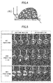
- A solder paste using a solder powder with a Sn-57Bi-1Ag composition was printed onto copper lands measuring 0.5 mm in diameter formed on a printed circuit board like that shown in
Figure 5 . One or two preforms having a Sn-3.0Ag-0.5Cu composition and measuring 0.5 mm x 0.25 mm were placed atop each land which had been printed with the solder paste, and reflow soldering was carried out at 200°C, which is the usual heating condition for a solder paste with a Sn-57Bi-1Ag solder composition. - This test ascertained the amount of a preform added to a solder paste of a Sn-Bi composition. With addition of one preform, the ratio of the weight of the solder paste to the weight of the preform was 1:1.6, and with addition of two preforms, it was 1:3.2.
- The soldered state after reflow soldering was observed to ascertain whether it was possible to perform soldering under usual reflow conditions for a low-temperature solder.
- It was confirmed that with one preform, the solder components of the solder paste and the solder components of the preform were mixed together and could not be distinguished from one another. In contrast, with two preforms, the solder joints became angular indicating that the solder components of the preform did not completely mix.
-
-
Figure 1 shows a broken portion of a land which was soldered with just a SnBi solder paste. -
Figure 2 is a figure showing that a solder joint which was soldered with just a SnBi solder paste broke in the solder portion. -
Figure 3 shows a broken portion of a land which was soldered by a soldering method according to the present invention in which a preform was added to a SnBi solder paste. -
Figure 4 is a figure showing that a solder joint which was formed by the soldering method according to the present invention in which a preform was added to a SnBi solder paste broke in the land portion. -
Figure 5 is a figure showing the results of a wettability test in Example 2. -
- 1. solder; 2. copper land
Claims (4)
- A soldering method using a SnBi-based low-temperature solder paste, wherein at least one type of preform selected from a Sn-Ag, Sn-Cu, and Sn-Ag-Cu solder composition is supplied to atop a printed solder paste to diffuse at least one solder composition selected from a Sn-Ag, a Sn-Cu, and a Sn-Ag-Cu solder composition into a SnBi-based low-temperature solder.
- A soldering method using a solder paste as set forth in claim 1 wherein the soldering method using a solder paste made of a SnBi-based low-temperature solder is characterized by using a low-temperature solder paste made by mixing a solder powder having a composition of at least 35% and at most 60% of Bi and a remainder of Sn or a solder powder of the foregoing composition to which at most 3% of Ag is added with a flux.
- A soldering method using a solder paste as set forth in claim 1 or claim 2 characterized in that the at least one type of preform selected from a Sn-Ag, a Sn-Cu, and a Sn-Ag-Cu solder composition is at least one type of preform selected from a preform having a composition of at least 0.3 to at most 4.0 mass% of Ag and a remainder of Sn, a preform having a composition of at least 0.3 to at most 1.2 mass% of Cu and a remainder of Sn, and a preform having a composition of at least 0.3 to at most 4.0 mass% of Ag, at least 0.3 to at most 1.2 mass% of Cu, and a remainder of Sn.
- A soldering method using a solder paste as set forth in any of claims 1 - 3 characterized in that the amount of the preform added to the solder paste is at least 0.7 to at most 75 mass% of the amount of the solder paste.
Applications Claiming Priority (1)
| Application Number | Priority Date | Filing Date | Title |
|---|---|---|---|
| PCT/JP2012/076631 WO2014061085A1 (en) | 2012-10-15 | 2012-10-15 | Soldering method for low-temperature solder paste |
Publications (3)
| Publication Number | Publication Date |
|---|---|
| EP2908612A1 true EP2908612A1 (en) | 2015-08-19 |
| EP2908612A4 EP2908612A4 (en) | 2016-06-22 |
| EP2908612B1 EP2908612B1 (en) | 2018-05-09 |
Family
ID=50487675
Family Applications (1)
| Application Number | Title | Priority Date | Filing Date |
|---|---|---|---|
| EP12886725.6A Active EP2908612B1 (en) | 2012-10-15 | 2012-10-15 | Soldering method for low-temperature solder paste |
Country Status (6)
| Country | Link |
|---|---|
| US (1) | US9402321B2 (en) |
| EP (1) | EP2908612B1 (en) |
| JP (1) | JP5796685B2 (en) |
| KR (1) | KR101587076B1 (en) |
| CN (1) | CN104737630B (en) |
| WO (1) | WO2014061085A1 (en) |
Families Citing this family (9)
| Publication number | Priority date | Publication date | Assignee | Title |
|---|---|---|---|---|
| CN108098092A (en) * | 2017-12-21 | 2018-06-01 | 成都川美新技术股份有限公司 | A kind of method being sintered using solder(ing) paste to radio frequency substrate and housing |
| CN111936264A (en) * | 2018-04-13 | 2020-11-13 | 千住金属工业株式会社 | solder paste |
| CN110549030A (en) * | 2019-08-23 | 2019-12-10 | 江苏太阳科技股份有限公司 | low-temperature solder for photovoltaic solder strip of HIT heterojunction and preparation method |
| KR102850024B1 (en) | 2019-12-27 | 2025-08-25 | 가부시끼가이샤 레조낙 | Connection structure and method for manufacturing the connection structure |
| KR102371636B1 (en) * | 2020-04-23 | 2022-03-07 | 제엠제코(주) | Method for fabricating semiconductor having double-sided substrate |
| DE102021103360A1 (en) | 2021-02-05 | 2022-08-11 | Few Fahrzeugelektrik Werk Gmbh & Co. Kg | Method of making a pre-tinning assembly and such pre-tinning assembly |
| CN113319454B (en) * | 2021-04-29 | 2022-08-23 | 中国电子科技集团公司第二十九研究所 | Solder presetting method for welding end of surface-mounted self-contained solid solder connector |
| KR20240019350A (en) * | 2021-06-11 | 2024-02-14 | 인듐 코포레이션 | High reliability lead-free solder paste with mixed solder alloy powder |
| KR102852732B1 (en) * | 2021-10-07 | 2025-08-29 | 엠케이전자 주식회사 | Lead-free solder alloy and method of fabricating electronic device using the same |
Family Cites Families (41)
| Publication number | Priority date | Publication date | Assignee | Title |
|---|---|---|---|---|
| US5320272A (en) * | 1993-04-02 | 1994-06-14 | Motorola, Inc. | Tin-bismuth solder connection having improved high temperature properties, and process for forming same |
| JPH06296080A (en) * | 1993-04-08 | 1994-10-21 | Sony Corp | Electronic component mounting board and electronic component mounting method |
| US5551627A (en) | 1994-09-29 | 1996-09-03 | Motorola, Inc. | Alloy solder connect assembly and method of connection |
| JP3347512B2 (en) | 1995-03-17 | 2002-11-20 | 富士通株式会社 | Solder alloy for low-temperature bonding, electronic device using the same, and method of manufacturing the same |
| JP2000307228A (en) * | 1999-04-22 | 2000-11-02 | Mitsubishi Electric Corp | Lead-free solder joining method and electronic module manufactured by the same |
| US6896172B2 (en) * | 2000-08-22 | 2005-05-24 | Senju Metal Industry Co., Ltd. | Lead-free solder paste for reflow soldering |
| JP4438974B2 (en) * | 2000-10-05 | 2010-03-24 | 千住金属工業株式会社 | Solder paste |
| JP4103591B2 (en) * | 2000-11-29 | 2008-06-18 | 千住金属工業株式会社 | Solder paste |
| JP2003234433A (en) * | 2001-10-01 | 2003-08-22 | Matsushita Electric Ind Co Ltd | Semiconductor device, method of mounting semiconductor device, and package and method of manufacturing the same |
| US6805974B2 (en) * | 2002-02-15 | 2004-10-19 | International Business Machines Corporation | Lead-free tin-silver-copper alloy solder composition |
| CN1445049A (en) * | 2002-03-19 | 2003-10-01 | 日本胜利株式会社 | Soldering tin paste, welding finished product and welding method |
| JP2004056065A (en) * | 2002-05-30 | 2004-02-19 | Hitachi Ltd | Electronic substrate manufacturing method |
| TW200600975A (en) * | 2004-02-20 | 2006-01-01 | Jsr Corp | Bilayer laminated film for bump formation and method of bump formation |
| KR101026970B1 (en) * | 2005-05-25 | 2011-04-11 | 센주긴조쿠고교 가부시키가이샤 | Lead free solder paste |
| JP4799997B2 (en) * | 2005-10-25 | 2011-10-26 | 富士通株式会社 | Method for manufacturing printed circuit board for electronic device and electronic device using the same |
| US9162324B2 (en) * | 2005-11-11 | 2015-10-20 | Senju Metal Industry Co., Ltd. | Solder paste and solder joint |
| US9175368B2 (en) * | 2005-12-13 | 2015-11-03 | Indium Corporation | MN doped SN-base solder alloy and solder joints thereof with superior drop shock reliability |
| KR100790978B1 (en) * | 2006-01-24 | 2008-01-02 | 삼성전자주식회사 | Bonding method at low temperature, and semiconductor package mounting method using same |
| US8388724B2 (en) * | 2006-04-26 | 2013-03-05 | Senju Metal Industry Co., Ltd. | Solder paste |
| WO2008004531A2 (en) * | 2006-07-05 | 2008-01-10 | Fuji Electric Holdings Co., Ltd. | Cream solder and method of soldering electronic part |
| US8293370B2 (en) * | 2006-08-04 | 2012-10-23 | Panasonic Corporation | Bonding material, bonded portion and circuit board |
| JP5266235B2 (en) * | 2006-10-17 | 2013-08-21 | フライズ・メタルズ・インコーポレイテッド | Method for providing an electrical connection in an electrical device |
| JP5373464B2 (en) * | 2008-04-23 | 2013-12-18 | パナソニック株式会社 | Conductive paste and mounting structure using the same |
| JP2009283628A (en) * | 2008-05-21 | 2009-12-03 | Tamura Seisakusho Co Ltd | Method for mounting semiconductor element |
| JP2012504179A (en) * | 2008-09-26 | 2012-02-16 | フライズ・メタルズ・インコーポレイテッド | Lead-free conductive composition and method using the same |
| KR101276147B1 (en) * | 2009-09-03 | 2013-06-18 | 가부시키가이샤 무라타 세이사쿠쇼 | Soldering paste, bonding method using same, and bonding structure |
| KR101660787B1 (en) * | 2009-09-23 | 2016-10-11 | 삼성전자주식회사 | Method of jointing a solder ball and method of repairing memory module |
| US9017446B2 (en) * | 2010-05-03 | 2015-04-28 | Indium Corporation | Mixed alloy solder paste |
| US9636784B2 (en) * | 2010-05-03 | 2017-05-02 | Indium Corporation | Mixed alloy solder paste |
| JP2011253853A (en) * | 2010-05-31 | 2011-12-15 | Sony Corp | Method of solder joint |
| CN102441717A (en) * | 2010-07-27 | 2012-05-09 | 应用材料公司 | Methods of soldering to high efficiency thin film solar panels |
| JP2012174332A (en) * | 2011-02-17 | 2012-09-10 | Fujitsu Ltd | Conductive jointing material, method of jointing conductor, and method of manufacturing semiconductor |
| DE102011013172A1 (en) * | 2011-02-28 | 2012-08-30 | Fraunhofer-Gesellschaft zur Förderung der angewandten Forschung e.V. | Paste for joining components of electronic power modules, system and method for applying the paste |
| CN103314652A (en) * | 2012-01-17 | 2013-09-18 | 松下电器产业株式会社 | Wiring substrate and production method therefor |
| US9795036B2 (en) * | 2012-05-10 | 2017-10-17 | Panasonic Intellectual Property Management Co., Ltd. | Mounting structure and method for manufacturing same |
| WO2014002304A1 (en) * | 2012-06-29 | 2014-01-03 | ハリマ化成株式会社 | Solder alloy, solder paste, and electronic circuit board |
| JP5238088B1 (en) * | 2012-06-29 | 2013-07-17 | ハリマ化成株式会社 | Solder alloy, solder paste and electronic circuit board |
| JP5893528B2 (en) * | 2012-07-27 | 2016-03-23 | 新日鉄住金マテリアルズ株式会社 | Lead-free solder bump bonding structure |
| KR20150039669A (en) * | 2012-08-02 | 2015-04-13 | 가부시키가이샤 다니구로구미 | Component having an electrode corrosion preventing layer and a method for manufacturing the component |
| JP6197319B2 (en) * | 2013-03-21 | 2017-09-20 | 富士通株式会社 | Mounting method of semiconductor element |
| JP6221499B2 (en) * | 2013-08-19 | 2017-11-01 | 富士通株式会社 | Electronic device and method of manufacturing electronic device |
-
2012
- 2012-10-15 WO PCT/JP2012/076631 patent/WO2014061085A1/en not_active Ceased
- 2012-10-15 CN CN201280076433.4A patent/CN104737630B/en active Active
- 2012-10-15 EP EP12886725.6A patent/EP2908612B1/en active Active
- 2012-10-15 JP JP2014541836A patent/JP5796685B2/en active Active
- 2012-10-15 US US14/435,333 patent/US9402321B2/en active Active
- 2012-10-15 KR KR1020157007749A patent/KR101587076B1/en active Active
Also Published As
| Publication number | Publication date |
|---|---|
| US9402321B2 (en) | 2016-07-26 |
| US20150282332A1 (en) | 2015-10-01 |
| EP2908612B1 (en) | 2018-05-09 |
| KR20150048208A (en) | 2015-05-06 |
| KR101587076B1 (en) | 2016-01-20 |
| CN104737630B (en) | 2016-02-03 |
| JPWO2014061085A1 (en) | 2016-09-05 |
| EP2908612A4 (en) | 2016-06-22 |
| JP5796685B2 (en) | 2015-10-21 |
| CN104737630A (en) | 2015-06-24 |
| WO2014061085A1 (en) | 2014-04-24 |
Similar Documents
| Publication | Publication Date | Title |
|---|---|---|
| EP2908612B1 (en) | Soldering method for low-temperature solder paste | |
| US20230330788A1 (en) | Lead-free and antimony-free tin solder reliable at high temperatures | |
| EP2689885B1 (en) | Lead-free solder alloy | |
| CN100491053C (en) | Solder paste and printed circuit board | |
| EP2422918B1 (en) | Soldering material and electronic component assembly | |
| US10322471B2 (en) | Low temperature high reliability alloy for solder hierarchy | |
| EP2692478B1 (en) | Lead-free solder ball | |
| JP4968381B2 (en) | Lead-free solder | |
| KR101738841B1 (en) | HIGH-TEMPERATURE SOLDER JOINT COMPRISING Bi-Sn-BASED HIGH-TEMPERATURE SOLDER ALLOY | |
| EP3903993A1 (en) | Lead-free solder alloy, solder joining material, electronic circuit mounting board, and electronic control device | |
| WO2022261130A1 (en) | High reliability lead-free solder pastes with mixed solder alloy powders | |
| KR100671394B1 (en) | Reflow soldering method and mixed mounting method and mixed mounting structure using PPS-free solder alloy | |
| EP2747933B1 (en) | A mn doped sn-base solder alloy and solder joints thereof with superior drop shock reliability | |
| JP5160576B2 (en) | Solder paste, pin grid array package substrate and pin grid array package using the same, and method for manufacturing pin grid array package substrate | |
| JP2002178191A (en) | Low-temperature lead-free solder composition and electronic component mounting structure using the same | |
| JP2015205293A (en) | Solder paste, method for manufacturing electronic device, and electronic device | |
| JPWO2005089999A1 (en) | Lead-free solder balls | |
| JP2019126827A (en) | Lead-free solder alloy | |
| Puttlitz | Including Selection |
Legal Events
| Date | Code | Title | Description |
|---|---|---|---|
| PUAI | Public reference made under article 153(3) epc to a published international application that has entered the european phase |
Free format text: ORIGINAL CODE: 0009012 |
|
| 17P | Request for examination filed |
Effective date: 20150410 |
|
| AK | Designated contracting states |
Kind code of ref document: A1 Designated state(s): AL AT BE BG CH CY CZ DE DK EE ES FI FR GB GR HR HU IE IS IT LI LT LU LV MC MK MT NL NO PL PT RO RS SE SI SK SM TR |
|
| AX | Request for extension of the european patent |
Extension state: BA ME |
|
| DAX | Request for extension of the european patent (deleted) | ||
| RA4 | Supplementary search report drawn up and despatched (corrected) |
Effective date: 20160520 |
|
| RIC1 | Information provided on ipc code assigned before grant |
Ipc: H05K 3/34 20060101AFI20160513BHEP |
|
| 17Q | First examination report despatched |
Effective date: 20170404 |
|
| REG | Reference to a national code |
Ref country code: DE Ref legal event code: R079 Ref document number: 602012046288 Country of ref document: DE Free format text: PREVIOUS MAIN CLASS: H05K0003340000 Ipc: B23K0035260000 |
|
| GRAP | Despatch of communication of intention to grant a patent |
Free format text: ORIGINAL CODE: EPIDOSNIGR1 |
|
| RIC1 | Information provided on ipc code assigned before grant |
Ipc: B23K 35/26 20060101AFI20171114BHEP Ipc: B23K 35/24 20060101ALI20171114BHEP Ipc: B23K 35/02 20060101ALI20171114BHEP Ipc: B23K 35/40 20060101ALI20171114BHEP Ipc: C22C 13/02 20060101ALI20171114BHEP Ipc: B23K 1/00 20060101ALI20171114BHEP Ipc: H05K 3/34 20060101ALI20171114BHEP Ipc: C22C 12/00 20060101ALI20171114BHEP |
|
| INTG | Intention to grant announced |
Effective date: 20171130 |
|
| GRAS | Grant fee paid |
Free format text: ORIGINAL CODE: EPIDOSNIGR3 |
|
| GRAA | (expected) grant |
Free format text: ORIGINAL CODE: 0009210 |
|
| AK | Designated contracting states |
Kind code of ref document: B1 Designated state(s): AL AT BE BG CH CY CZ DE DK EE ES FI FR GB GR HR HU IE IS IT LI LT LU LV MC MK MT NL NO PL PT RO RS SE SI SK SM TR |
|
| REG | Reference to a national code |
Ref country code: GB Ref legal event code: FG4D |
|
| REG | Reference to a national code |
Ref country code: CH Ref legal event code: EP Ref country code: AT Ref legal event code: REF Ref document number: 997142 Country of ref document: AT Kind code of ref document: T Effective date: 20180515 |
|
| REG | Reference to a national code |
Ref country code: IE Ref legal event code: FG4D |
|
| REG | Reference to a national code |
Ref country code: DE Ref legal event code: R096 Ref document number: 602012046288 Country of ref document: DE |
|
| REG | Reference to a national code |
Ref country code: NL Ref legal event code: MP Effective date: 20180509 |
|
| REG | Reference to a national code |
Ref country code: LT Ref legal event code: MG4D |
|
| REG | Reference to a national code |
Ref country code: SK Ref legal event code: T3 Ref document number: E 27572 Country of ref document: SK |
|
| PG25 | Lapsed in a contracting state [announced via postgrant information from national office to epo] |
Ref country code: BG Free format text: LAPSE BECAUSE OF FAILURE TO SUBMIT A TRANSLATION OF THE DESCRIPTION OR TO PAY THE FEE WITHIN THE PRESCRIBED TIME-LIMIT Effective date: 20180809 Ref country code: NO Free format text: LAPSE BECAUSE OF FAILURE TO SUBMIT A TRANSLATION OF THE DESCRIPTION OR TO PAY THE FEE WITHIN THE PRESCRIBED TIME-LIMIT Effective date: 20180809 Ref country code: FI Free format text: LAPSE BECAUSE OF FAILURE TO SUBMIT A TRANSLATION OF THE DESCRIPTION OR TO PAY THE FEE WITHIN THE PRESCRIBED TIME-LIMIT Effective date: 20180509 Ref country code: LT Free format text: LAPSE BECAUSE OF FAILURE TO SUBMIT A TRANSLATION OF THE DESCRIPTION OR TO PAY THE FEE WITHIN THE PRESCRIBED TIME-LIMIT Effective date: 20180509 Ref country code: SE Free format text: LAPSE BECAUSE OF FAILURE TO SUBMIT A TRANSLATION OF THE DESCRIPTION OR TO PAY THE FEE WITHIN THE PRESCRIBED TIME-LIMIT Effective date: 20180509 Ref country code: ES Free format text: LAPSE BECAUSE OF FAILURE TO SUBMIT A TRANSLATION OF THE DESCRIPTION OR TO PAY THE FEE WITHIN THE PRESCRIBED TIME-LIMIT Effective date: 20180509 |
|
| PG25 | Lapsed in a contracting state [announced via postgrant information from national office to epo] |
Ref country code: NL Free format text: LAPSE BECAUSE OF FAILURE TO SUBMIT A TRANSLATION OF THE DESCRIPTION OR TO PAY THE FEE WITHIN THE PRESCRIBED TIME-LIMIT Effective date: 20180509 Ref country code: RS Free format text: LAPSE BECAUSE OF FAILURE TO SUBMIT A TRANSLATION OF THE DESCRIPTION OR TO PAY THE FEE WITHIN THE PRESCRIBED TIME-LIMIT Effective date: 20180509 Ref country code: LV Free format text: LAPSE BECAUSE OF FAILURE TO SUBMIT A TRANSLATION OF THE DESCRIPTION OR TO PAY THE FEE WITHIN THE PRESCRIBED TIME-LIMIT Effective date: 20180509 Ref country code: GR Free format text: LAPSE BECAUSE OF FAILURE TO SUBMIT A TRANSLATION OF THE DESCRIPTION OR TO PAY THE FEE WITHIN THE PRESCRIBED TIME-LIMIT Effective date: 20180810 Ref country code: HR Free format text: LAPSE BECAUSE OF FAILURE TO SUBMIT A TRANSLATION OF THE DESCRIPTION OR TO PAY THE FEE WITHIN THE PRESCRIBED TIME-LIMIT Effective date: 20180509 |
|
| REG | Reference to a national code |
Ref country code: AT Ref legal event code: MK05 Ref document number: 997142 Country of ref document: AT Kind code of ref document: T Effective date: 20180509 |
|
| PG25 | Lapsed in a contracting state [announced via postgrant information from national office to epo] |
Ref country code: PL Free format text: LAPSE BECAUSE OF FAILURE TO SUBMIT A TRANSLATION OF THE DESCRIPTION OR TO PAY THE FEE WITHIN THE PRESCRIBED TIME-LIMIT Effective date: 20180509 Ref country code: AT Free format text: LAPSE BECAUSE OF FAILURE TO SUBMIT A TRANSLATION OF THE DESCRIPTION OR TO PAY THE FEE WITHIN THE PRESCRIBED TIME-LIMIT Effective date: 20180509 Ref country code: EE Free format text: LAPSE BECAUSE OF FAILURE TO SUBMIT A TRANSLATION OF THE DESCRIPTION OR TO PAY THE FEE WITHIN THE PRESCRIBED TIME-LIMIT Effective date: 20180509 Ref country code: DK Free format text: LAPSE BECAUSE OF FAILURE TO SUBMIT A TRANSLATION OF THE DESCRIPTION OR TO PAY THE FEE WITHIN THE PRESCRIBED TIME-LIMIT Effective date: 20180509 Ref country code: RO Free format text: LAPSE BECAUSE OF FAILURE TO SUBMIT A TRANSLATION OF THE DESCRIPTION OR TO PAY THE FEE WITHIN THE PRESCRIBED TIME-LIMIT Effective date: 20180509 |
|
| REG | Reference to a national code |
Ref country code: DE Ref legal event code: R097 Ref document number: 602012046288 Country of ref document: DE |
|
| PG25 | Lapsed in a contracting state [announced via postgrant information from national office to epo] |
Ref country code: SM Free format text: LAPSE BECAUSE OF FAILURE TO SUBMIT A TRANSLATION OF THE DESCRIPTION OR TO PAY THE FEE WITHIN THE PRESCRIBED TIME-LIMIT Effective date: 20180509 Ref country code: IT Free format text: LAPSE BECAUSE OF FAILURE TO SUBMIT A TRANSLATION OF THE DESCRIPTION OR TO PAY THE FEE WITHIN THE PRESCRIBED TIME-LIMIT Effective date: 20180509 |
|
| PLBE | No opposition filed within time limit |
Free format text: ORIGINAL CODE: 0009261 |
|
| STAA | Information on the status of an ep patent application or granted ep patent |
Free format text: STATUS: NO OPPOSITION FILED WITHIN TIME LIMIT |
|
| 26N | No opposition filed |
Effective date: 20190212 |
|
| PG25 | Lapsed in a contracting state [announced via postgrant information from national office to epo] |
Ref country code: SI Free format text: LAPSE BECAUSE OF FAILURE TO SUBMIT A TRANSLATION OF THE DESCRIPTION OR TO PAY THE FEE WITHIN THE PRESCRIBED TIME-LIMIT Effective date: 20180509 |
|
| REG | Reference to a national code |
Ref country code: CH Ref legal event code: PL |
|
| GBPC | Gb: european patent ceased through non-payment of renewal fee |
Effective date: 20181015 |
|
| REG | Reference to a national code |
Ref country code: BE Ref legal event code: MM Effective date: 20181031 |
|
| PG25 | Lapsed in a contracting state [announced via postgrant information from national office to epo] |
Ref country code: MC Free format text: LAPSE BECAUSE OF FAILURE TO SUBMIT A TRANSLATION OF THE DESCRIPTION OR TO PAY THE FEE WITHIN THE PRESCRIBED TIME-LIMIT Effective date: 20180509 Ref country code: LU Free format text: LAPSE BECAUSE OF NON-PAYMENT OF DUE FEES Effective date: 20181015 |
|
| REG | Reference to a national code |
Ref country code: IE Ref legal event code: MM4A |
|
| PG25 | Lapsed in a contracting state [announced via postgrant information from national office to epo] |
Ref country code: BE Free format text: LAPSE BECAUSE OF NON-PAYMENT OF DUE FEES Effective date: 20181031 Ref country code: CH Free format text: LAPSE BECAUSE OF NON-PAYMENT OF DUE FEES Effective date: 20181031 Ref country code: LI Free format text: LAPSE BECAUSE OF NON-PAYMENT OF DUE FEES Effective date: 20181031 Ref country code: FR Free format text: LAPSE BECAUSE OF NON-PAYMENT OF DUE FEES Effective date: 20181031 |
|
| PG25 | Lapsed in a contracting state [announced via postgrant information from national office to epo] |
Ref country code: IE Free format text: LAPSE BECAUSE OF NON-PAYMENT OF DUE FEES Effective date: 20181015 Ref country code: GB Free format text: LAPSE BECAUSE OF NON-PAYMENT OF DUE FEES Effective date: 20181015 |
|
| PG25 | Lapsed in a contracting state [announced via postgrant information from national office to epo] |
Ref country code: AL Free format text: LAPSE BECAUSE OF FAILURE TO SUBMIT A TRANSLATION OF THE DESCRIPTION OR TO PAY THE FEE WITHIN THE PRESCRIBED TIME-LIMIT Effective date: 20180509 |
|
| PG25 | Lapsed in a contracting state [announced via postgrant information from national office to epo] |
Ref country code: MT Free format text: LAPSE BECAUSE OF NON-PAYMENT OF DUE FEES Effective date: 20181015 |
|
| PG25 | Lapsed in a contracting state [announced via postgrant information from national office to epo] |
Ref country code: TR Free format text: LAPSE BECAUSE OF FAILURE TO SUBMIT A TRANSLATION OF THE DESCRIPTION OR TO PAY THE FEE WITHIN THE PRESCRIBED TIME-LIMIT Effective date: 20180509 |
|
| PG25 | Lapsed in a contracting state [announced via postgrant information from national office to epo] |
Ref country code: PT Free format text: LAPSE BECAUSE OF FAILURE TO SUBMIT A TRANSLATION OF THE DESCRIPTION OR TO PAY THE FEE WITHIN THE PRESCRIBED TIME-LIMIT Effective date: 20180509 |
|
| PG25 | Lapsed in a contracting state [announced via postgrant information from national office to epo] |
Ref country code: MK Free format text: LAPSE BECAUSE OF NON-PAYMENT OF DUE FEES Effective date: 20180509 Ref country code: CY Free format text: LAPSE BECAUSE OF FAILURE TO SUBMIT A TRANSLATION OF THE DESCRIPTION OR TO PAY THE FEE WITHIN THE PRESCRIBED TIME-LIMIT Effective date: 20180509 Ref country code: HU Free format text: LAPSE BECAUSE OF FAILURE TO SUBMIT A TRANSLATION OF THE DESCRIPTION OR TO PAY THE FEE WITHIN THE PRESCRIBED TIME-LIMIT; INVALID AB INITIO Effective date: 20121015 |
|
| PG25 | Lapsed in a contracting state [announced via postgrant information from national office to epo] |
Ref country code: IS Free format text: LAPSE BECAUSE OF FAILURE TO SUBMIT A TRANSLATION OF THE DESCRIPTION OR TO PAY THE FEE WITHIN THE PRESCRIBED TIME-LIMIT Effective date: 20180909 |
|
| PGFP | Annual fee paid to national office [announced via postgrant information from national office to epo] |
Ref country code: SK Payment date: 20250912 Year of fee payment: 14 |
|
| PGFP | Annual fee paid to national office [announced via postgrant information from national office to epo] |
Ref country code: DE Payment date: 20250902 Year of fee payment: 14 |
|
| PGFP | Annual fee paid to national office [announced via postgrant information from national office to epo] |
Ref country code: CZ Payment date: 20251002 Year of fee payment: 14 |