EP2908398A2 - Hybrid circuit breaker with superconducting fault current limiter - Google Patents
Hybrid circuit breaker with superconducting fault current limiter Download PDFInfo
- Publication number
- EP2908398A2 EP2908398A2 EP15154807.0A EP15154807A EP2908398A2 EP 2908398 A2 EP2908398 A2 EP 2908398A2 EP 15154807 A EP15154807 A EP 15154807A EP 2908398 A2 EP2908398 A2 EP 2908398A2
- Authority
- EP
- European Patent Office
- Prior art keywords
- semiconductor switch
- switch unit
- circuit breaker
- resistor
- circuit
- Prior art date
- Legal status (The legal status is an assumption and is not a legal conclusion. Google has not performed a legal analysis and makes no representation as to the accuracy of the status listed.)
- Granted
Links
- 239000004065 semiconductor Substances 0.000 claims abstract description 128
- 238000010586 diagram Methods 0.000 description 8
- 238000010891 electric arc Methods 0.000 description 6
- 239000003990 capacitor Substances 0.000 description 3
- 239000000463 material Substances 0.000 description 3
- 238000012986 modification Methods 0.000 description 2
- 230000004048 modification Effects 0.000 description 2
- 230000001052 transient effect Effects 0.000 description 2
- 230000007423 decrease Effects 0.000 description 1
- 238000000034 method Methods 0.000 description 1
Images



Classifications
-
- H—ELECTRICITY
- H02—GENERATION; CONVERSION OR DISTRIBUTION OF ELECTRIC POWER
- H02H—EMERGENCY PROTECTIVE CIRCUIT ARRANGEMENTS
- H02H9/00—Emergency protective circuit arrangements for limiting excess current or voltage without disconnection
- H02H9/02—Emergency protective circuit arrangements for limiting excess current or voltage without disconnection responsive to excess current
- H02H9/023—Current limitation using superconducting elements
-
- H—ELECTRICITY
- H02—GENERATION; CONVERSION OR DISTRIBUTION OF ELECTRIC POWER
- H02H—EMERGENCY PROTECTIVE CIRCUIT ARRANGEMENTS
- H02H7/00—Emergency protective circuit arrangements specially adapted for specific types of electric machines or apparatus or for sectionalised protection of cable or line systems, and effecting automatic switching in the event of an undesired change from normal working conditions
- H02H7/001—Emergency protective circuit arrangements specially adapted for specific types of electric machines or apparatus or for sectionalised protection of cable or line systems, and effecting automatic switching in the event of an undesired change from normal working conditions for superconducting apparatus, e.g. coils, lines, machines
-
- H—ELECTRICITY
- H01—ELECTRIC ELEMENTS
- H01H—ELECTRIC SWITCHES; RELAYS; SELECTORS; EMERGENCY PROTECTIVE DEVICES
- H01H33/00—High-tension or heavy-current switches with arc-extinguishing or arc-preventing means
- H01H33/02—Details
- H01H33/59—Circuit arrangements not adapted to a particular application of the switch and not otherwise provided for, e.g. for ensuring operation of the switch at a predetermined point in the AC cycle
- H01H33/596—Circuit arrangements not adapted to a particular application of the switch and not otherwise provided for, e.g. for ensuring operation of the switch at a predetermined point in the AC cycle for interrupting DC
-
- H—ELECTRICITY
- H01—ELECTRIC ELEMENTS
- H01H—ELECTRIC SWITCHES; RELAYS; SELECTORS; EMERGENCY PROTECTIVE DEVICES
- H01H9/00—Details of switching devices, not covered by groups H01H1/00 - H01H7/00
- H01H9/54—Circuit arrangements not adapted to a particular application of the switching device and for which no provision exists elsewhere
- H01H9/548—Electromechanical and static switch connected in series
-
- H—ELECTRICITY
- H02—GENERATION; CONVERSION OR DISTRIBUTION OF ELECTRIC POWER
- H02H—EMERGENCY PROTECTIVE CIRCUIT ARRANGEMENTS
- H02H3/00—Emergency protective circuit arrangements for automatic disconnection directly responsive to an undesired change from normal electric working condition with or without subsequent reconnection ; integrated protection
- H02H3/02—Details
- H02H3/025—Disconnection after limiting, e.g. when limiting is not sufficient or for facilitating disconnection
-
- H—ELECTRICITY
- H02—GENERATION; CONVERSION OR DISTRIBUTION OF ELECTRIC POWER
- H02H—EMERGENCY PROTECTIVE CIRCUIT ARRANGEMENTS
- H02H3/00—Emergency protective circuit arrangements for automatic disconnection directly responsive to an undesired change from normal electric working condition with or without subsequent reconnection ; integrated protection
- H02H3/08—Emergency protective circuit arrangements for automatic disconnection directly responsive to an undesired change from normal electric working condition with or without subsequent reconnection ; integrated protection responsive to excess current
- H02H3/087—Emergency protective circuit arrangements for automatic disconnection directly responsive to an undesired change from normal electric working condition with or without subsequent reconnection ; integrated protection responsive to excess current for DC applications
-
- H—ELECTRICITY
- H02—GENERATION; CONVERSION OR DISTRIBUTION OF ELECTRIC POWER
- H02H—EMERGENCY PROTECTIVE CIRCUIT ARRANGEMENTS
- H02H7/00—Emergency protective circuit arrangements specially adapted for specific types of electric machines or apparatus or for sectionalised protection of cable or line systems, and effecting automatic switching in the event of an undesired change from normal working conditions
- H02H7/22—Emergency protective circuit arrangements specially adapted for specific types of electric machines or apparatus or for sectionalised protection of cable or line systems, and effecting automatic switching in the event of an undesired change from normal working conditions for distribution gear, e.g. bus-bar systems; for switching devices
- H02H7/222—Emergency protective circuit arrangements specially adapted for specific types of electric machines or apparatus or for sectionalised protection of cable or line systems, and effecting automatic switching in the event of an undesired change from normal working conditions for distribution gear, e.g. bus-bar systems; for switching devices for switches
-
- H—ELECTRICITY
- H01—ELECTRIC ELEMENTS
- H01H—ELECTRIC SWITCHES; RELAYS; SELECTORS; EMERGENCY PROTECTIVE DEVICES
- H01H9/00—Details of switching devices, not covered by groups H01H1/00 - H01H7/00
- H01H9/54—Circuit arrangements not adapted to a particular application of the switching device and for which no provision exists elsewhere
- H01H9/541—Contacts shunted by semiconductor devices
- H01H9/542—Contacts shunted by static switch means
- H01H2009/543—Contacts shunted by static switch means third parallel branch comprising an energy absorber, e.g. MOV, PTC, Zener
-
- Y—GENERAL TAGGING OF NEW TECHNOLOGICAL DEVELOPMENTS; GENERAL TAGGING OF CROSS-SECTIONAL TECHNOLOGIES SPANNING OVER SEVERAL SECTIONS OF THE IPC; TECHNICAL SUBJECTS COVERED BY FORMER USPC CROSS-REFERENCE ART COLLECTIONS [XRACs] AND DIGESTS
- Y02—TECHNOLOGIES OR APPLICATIONS FOR MITIGATION OR ADAPTATION AGAINST CLIMATE CHANGE
- Y02E—REDUCTION OF GREENHOUSE GAS [GHG] EMISSIONS, RELATED TO ENERGY GENERATION, TRANSMISSION OR DISTRIBUTION
- Y02E40/00—Technologies for an efficient electrical power generation, transmission or distribution
- Y02E40/60—Superconducting electric elements or equipment; Power systems integrating superconducting elements or equipment
Definitions
- Embodiments of the present invention relate to a circuit breaker, and in particular, to a high-voltage circuit breaker.
- a current is relatively large in the circuit in case of an overcurrent fault (for example a short circuit). If a switch device is disconnected directly to interrupt the circuit, an arc discharge phenomenon may occur on the switch device, which does great harm to the switch device, greatly affects switch device performance, and even damages the switch device. With increasing capacity of a power grid, a short-circuit current also increases, and large arc discharge is easily caused upon disconnecting a switch device, thereby damaging a switch device.
- the present invention provides a circuit breaker.
- the circuit breaker includes a superconducting fault current limiter and a circuit breaker module, wherein the superconducting fault current limiter and the circuit breaker module are electrically connected in series, and the circuit breaker module includes a disconnector, a first semiconductor switch unit, and a second semiconductor switch unit.
- the disconnector is electrically connected in series with the first semiconductor switch unit, and also electrically connected in series with the superconducting fault current limiter
- the second semiconductor switch unit is electrically connected in parallel with the disconnector and first semiconductor switch unit that are electrically connected in series.
- the circuit breaker module includes a nonlinear resistor, and the nonlinear resistor and the second semiconductor switch unit are electrically connected in parallel.
- the disconnector and the first semiconductor switch unit are normally closed (e.g., in a conductive state or turned on), and the second semiconductor switch unit is normally open (e.g., in a non-conductive state or turned off.
- the circuit breaker module includes an LC resonant unit and a third semiconductor switch unit electrically connected in series with the LC resonant unit, and the second semiconductor switch unit is electrically connected in parallel with the LC resonant unit and the third semiconductor switch unit that are electrically connected in series.
- the circuit breaker module includes several diodes.
- the diodes are electrically connected in parallel with the second semiconductor switch unit and the third semiconductor switch unit respectively, and conducting directions of the diodes are respectively opposite to conducting directions of the second semiconductor switch unit and the third semiconductor switch unit that are electrically connected in parallel with the diodes.
- the circuit breaker module includes a nonlinear resistor, and the nonlinear resistor is electrically connected in parallel with the LC resonant unit and the third semiconductor switch unit.
- the third semiconductor switch unit is normally open (e.g., in a non-conductive state or turned off).
- the disconnector, the first semiconductor switch unit, the second semiconductor switch unit, and the third semiconductor switch unit are controllable devices.
- the first semiconductor switch unit and the second semiconductor switch unit include at least one semiconductor switch device respectively.
- the superconducting fault current limiter includes a superconducting resistor, a resistor, and an inductor.
- the resistor and the inductor are electrically connected in series, and the superconducting resistor is electrically connected in parallel with the resistor and the inductor that are electrically connected in series.
- FIG. 1 is a schematic diagram of a circuit breaker 10 according to an embodiment of the present invention.
- the circuit breaker 10 in the present embodiment is connected in series with a main switch 11 and power 13.
- the circuit breaker 10 includes a superconducting fault current limiter 15 and a circuit breaker module 17.
- the main switch 11, the power 13, the superconducting fault current limiter 15, and the circuit breaker module 17 are connected in series.
- the circuit breaker 10 can be applied to a high-voltage circuit, especially a high-voltage direct current circuit, for example, power grid, which is not limited thereto.
- the power 13 is high-voltage direct current power, for example, a high-voltage direct current power grid, a power generating equipment, or the like, and supplies high-voltage direct current power to a working circuit (not shown in the figure).
- the circuit breaker 10 is connected between the power 13 and the working circuit (not shown in the figure), and is used to quickly and securely cut off power when an overcurrent fault occurs on the circuit, for example, the circuit is short-circuit, transient current increase due to loads, and the like.
- the circuit breaker 10 When the circuit is running properly, the circuit breaker 10 is in a conductive state, and cuts off or accesses the power 13 by controlling the turning-on or the turning-off of the main switch 11.
- a current of the circuit increases dramatically.
- the main switch 11 is turned off if the current is greater than a rated short circuit breaking current of the main switch 11, and arc discharge may occur on the main switch 11.
- An embodiment of the present invention uses the circuit breaker 10 to interrupt the circuit.
- the superconducting fault current limiter 15 of the circuit breaker 10 first limits the current, and then disconnects the circuit through the circuit breaker module 17.
- the main switch 11 is turned off after the circuit breaker 10 interrupts the circuit, thereby preventing the main switch 11 from generating arc discharge.
- the main switch 11 is a mechanical switch, for example, a knife switch.
- FIG. 2 is a schematic diagram of the superconducting fault current limiter 15 of the circuit breaker 10 shown in FIG. 1 according to an embodiment.
- the superconducting fault current limiter 15 can limit a current in a circuit.
- the superconducting fault current limiter 15 in the present embodiment is a resistive superconducting fault current limiter.
- the superconducting fault current limiter 15 includes a superconducting resistor R sc , a resistor R shunt , and an inductor L shunt .
- the resistor R shunt and the inductor L shunt are connected in series, and the superconducting resistor R sc is connected in parallel with the resistor R shunt and the inductor L shunt that are connected in series.
- the superconducting resistor R sc is made of high-temperature superconducting materials. When the circuit is running properly, a current passing through the superconducting resistor R sc is less than a critical current of the superconducting resistor R sc . Because of characteristics of superconducting materials, the superconducting resistor R sc is in a superconducting state, and a resistance value is equal or close to zero.
- the branches of the resistor R shunt and the inductor L shunt limit increases of the voltages at both ends of the superconducting resistor R sc .
- the inductor L shunt limits a current.
- the superconducting fault current limiter 15 limits the current in the circuit. Because of characteristics of superconducting materials, the superconducting fault current limiter 15 can reduce the current within a few milliseconds. After the current in the circuit is reduced, the circuit breaker module 17 is disconnected, so as to cut off the power 13 from the circuit.
- the superconducting fault current limiter 15 may adopt another type of superconducting fault current limiter, such as, a noninductive reactance, or hybrid superconducting fault current limiter.
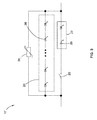
- FIG. 3 is a schematic diagram of a circuit breaker module 17 shown in FIG. 1 according to an embodiment.
- the circuit breaker module 17 includes a disconnector or isolator 20, a first semiconductor switch unit 22, and a second semiconductor switch unit 24.
- the disconnector 20 is connected in series with the first semiconductor switch unit 22, and also connected in series with the superconducting fault current limiter 15.
- the second semiconductor switch unit 24 is connected in parallel with the disconnector 20 and first semiconductor switch unit 22 that are connected in series.
- the disconnector 20 and the first semiconductor switch unit 22 are normally closed (i.e., in a conductive state or turned on), and the second semiconductor switch unit 24 is normally open (i.e., in a non-conductive state or turned off).
- the disconnector 20 is a fast high-voltage disconnector.
- the disconnector 20 may be a mechanical switch.
- the first semiconductor switch unit 22 and the second semiconductor switch unit 24 include at least one semiconductor switch device 26 respectively, such as, a thyristor, a Gate Turn-Off Thyristor (GTO), an Insulated Gate Bipolar Translator (IGBT), and the like.
- GTO Gate Turn-Off Thyristor
- IGBT Insulated Gate Bipolar Translator
- Multiple semiconductor switch devices 26 of the first semiconductor switch unit 22 are connected in series, and multiple semiconductor switch devices 26 of the second semiconductor switch unit 24 are connected in series to bear a high voltage.
- the first semiconductor switch unit 22 and the second semiconductor switch unit 24 adopt the same semiconductor switch device 26.
- first semiconductor switch unit 22 and the second semiconductor switch unit 24 adopt different semiconductor switch devices 26, for example, types, rated parameters, and performance of semiconductor switch devices 26 are different.
- An impedance of the second semiconductor switch unit 24 is greater than an impedance of the first semiconductor switch unit 22.
- the disconnector 20 and the first semiconductor switch unit 22 are in a conductive state, and a current passes through the disconnector 20 and the first semiconductor switch unit 22.
- the impedance of the first semiconductor switch unit 22 is relatively small; therefore, there is a relatively small impact on a current and voltage of the circuit.
- the second semiconductor switch unit 24 is closed (or turned on) to shunt. Then, the first semiconductor switch unit 22 is disconnected (or turned off), and a total current of the circuit passes through the second semiconductor switch unit 24. Then, the second semiconductor switch unit 24 and the disconnector 20 are disconnected (or turned off or opened). When a semiconductor switch is disconnected or turned off, no arc discharge occurs; therefore, the semiconductor switch can be quickly disconnected.
- the circuit is interrupted through the semiconductor switch, preventing an arc discharge phenomenon from occurring when the disconnector 20 and a main switch 11 are disconnected or opened directly in case of a high voltage and a large current, and protecting the disconnector 20 and the main switch 11.
- the circuit breaker module 17 can be quickly disconnected.
- the disconnector 20, the first semiconductor switch unit 22, and the second semiconductor switch unit 24 are controllable devices, and their turning-on and turning-off can be controlled through a controller (not shown in the figures).
- the circuit breaker module 17 further includes a nonlinear resistor 38.
- the nonlinear resistor 38 and the second semiconductor switch unit 24 are connected in parallel.
- the nonlinear resistor 38 can limit a transient voltage increase of the second semiconductor switch unit 24 when the second semiconductor switch unit 24 is disconnected, thereby preventing damage to the semiconductor switch device 26 of the second semiconductor switch unit 24.
- FIG. 4 is a schematic diagram of a circuit breaker module 17 shown in FIG. 1 according to another embodiment.
- the circuit breaker module 17 shown in FIG. 4 is similar to the circuit breaker module 17 shown in FIG. 3 .
- the circuit breaker module 17 shown in FIG. 4 further includes an LC resonant unit 28 and a third semiconductor switch unit 30 connected in series with the LC resonant unit 28.
- the second semiconductor switch unit 24 is connected in parallel with the LC resonant unit 28 and the third semiconductor switch unit 30 that are connected in series.
- the LC resonant unit 28 includes an inductor 32 and a capacitor 34 that are connected in series.
- the third semiconductor switch unit 30 is normally open (i.e., in a non-conductive state or turned off).
- the third semiconductor switch unit 30 is a controllable device.
- the third semiconductor switch unit 30 includes a semiconductor switch device, and the semiconductor switch device may be the same as the semiconductor switch device 26 of the first semiconductor switch unit 22 and/or the second semiconductor switch unit 24.
- the third semiconductor switch unit 30 includes multiple semiconductor switch devices connected in series.
- the circuit breaker module 17 includes several diodes 36.
- the diodes 36 are connected in parallel with the second semiconductor switch unit 24 and the third semiconductor switch unit 30 respectively, and conducting directions of the diodes 36 are respectively opposite to conducting directions of the second semiconductor switch unit 24 and the third semiconductor switch unit 30 that are connected in parallel with the diodes 36.
- Conducting directions of the semiconductor switch devices 26 of the first semiconductor switch unit 22, the second semiconductor switch unit 24, and the third semiconductor switch unit 30 are the same as a direction of a total current I Line of a main circuit.
- Conducting directions of the diodes 36 are opposite to the direction of the total current I Line of the main circuit.
- the circuit breaker module 17 further includes a nonlinear resistor 38.
- the nonlinear resistor 38 is connected in parallel with the LC resonant unit 28 and the third semiconductor switch unit 30. When a current passing through the nonlinear resistor 38 increases, a resistance value of the nonlinear resistor 38 decreases.
- the disconnector 20 and the first semiconductor switch unit 22 are in a conductive state. In this case, a resistance value of the nonlinear resistor 38 is very large, which has a relatively small impact on a current of the circuit.
- the second semiconductor switch unit 24 is closed (or turned on) to shunt, and the first semiconductor switch unit 22 is disconnected (or turned off). Then, the third semiconductor switch unit 30 is closed (or turned on). In this case, the LC resonant unit 28, the second semiconductor switch unit 24, the third semiconductor switch unit 30, and the diodes 36 form a resonant loop.
- the second semiconductor switch unit 24 and the third semiconductor switch unit 30 are disconnected (or turned off). Then, the disconnector 20 is disconnected (or opened). In some embodiments, after the first semiconductor switch unit 22 is disconnected, no current passes through the disconnector 20, and in this case, the disconnector 20 can be disconnected (or opened). Therefore, when a current passing through the second semiconductor switch unit 24 and the third semiconductor switch unit 30 is equal to zero, the second semiconductor switch unit 24 and the third semiconductor switch unit 30 are disconnected (or turned off), protecting the second semiconductor switch unit 24 and the third semiconductor switch unit 30. After the third semiconductor switch unit 30 is disconnected (or turned off), the capacitor 34 discharges through the diodes 36, and the nonlinear resistor 38 absorbs remaining energy of the capacitor 34.
Landscapes
- Engineering & Computer Science (AREA)
- Power Engineering (AREA)
- Emergency Protection Circuit Devices (AREA)
- Driving Mechanisms And Operating Circuits Of Arc-Extinguishing High-Tension Switches (AREA)
Abstract
Description
- Embodiments of the present invention relate to a circuit breaker, and in particular, to a high-voltage circuit breaker.
- In a high-voltage circuit, especially in a high-voltage direct current circuit, for example, power grid, a current is relatively large in the circuit in case of an overcurrent fault (for example a short circuit). If a switch device is disconnected directly to interrupt the circuit, an arc discharge phenomenon may occur on the switch device, which does great harm to the switch device, greatly affects switch device performance, and even damages the switch device. With increasing capacity of a power grid, a short-circuit current also increases, and large arc discharge is easily caused upon disconnecting a switch device, thereby damaging a switch device.
- Therefore, it is necessary to provide an improved circuit breaker to solve the foregoing technical problem.
- According to one aspect, the present invention provides a circuit breaker. The circuit breaker includes a superconducting fault current limiter and a circuit breaker module, wherein the superconducting fault current limiter and the circuit breaker module are electrically connected in series, and the circuit breaker module includes a disconnector, a first semiconductor switch unit, and a second semiconductor switch unit. In an embodiment, the disconnector is electrically connected in series with the first semiconductor switch unit, and also electrically connected in series with the superconducting fault current limiter, and the second semiconductor switch unit is electrically connected in parallel with the disconnector and first semiconductor switch unit that are electrically connected in series.
- In some embodiments, the circuit breaker module includes a nonlinear resistor, and the nonlinear resistor and the second semiconductor switch unit are electrically connected in parallel.
- In some embodiments, the disconnector and the first semiconductor switch unit are normally closed (e.g., in a conductive state or turned on), and the second semiconductor switch unit is normally open (e.g., in a non-conductive state or turned off.
- In some embodiments, the circuit breaker module includes an LC resonant unit and a third semiconductor switch unit electrically connected in series with the LC resonant unit, and the second semiconductor switch unit is electrically connected in parallel with the LC resonant unit and the third semiconductor switch unit that are electrically connected in series.
- In some embodiments, the circuit breaker module includes several diodes. The diodes are electrically connected in parallel with the second semiconductor switch unit and the third semiconductor switch unit respectively, and conducting directions of the diodes are respectively opposite to conducting directions of the second semiconductor switch unit and the third semiconductor switch unit that are electrically connected in parallel with the diodes.
- In some embodiments, the circuit breaker module includes a nonlinear resistor, and the nonlinear resistor is electrically connected in parallel with the LC resonant unit and the third semiconductor switch unit.
- In some embodiments, the third semiconductor switch unit is normally open (e.g., in a non-conductive state or turned off).
- In some embodiments, the disconnector, the first semiconductor switch unit, the second semiconductor switch unit, and the third semiconductor switch unit are controllable devices.
- In some embodiments, the first semiconductor switch unit and the second semiconductor switch unit include at least one semiconductor switch device respectively.
- In some embodiments, the superconducting fault current limiter includes a superconducting resistor, a resistor, and an inductor. The resistor and the inductor are electrically connected in series, and the superconducting resistor is electrically connected in parallel with the resistor and the inductor that are electrically connected in series.
- The present invention may be better understood through the description of embodiments of the present invention with reference to the accompanying drawings. In the accompanying drawings:
-
FIG. 1 is a schematic diagram of a circuit breaker according to an embodiment of the present invention; -
FIG. 2 is a schematic diagram of a superconducting fault current limiter of the circuit breaker shown inFIG. 1 ; -
FIG. 3 is a schematic diagram of a circuit breaker module of the circuit breaker shown inFIG. 1 ; and -
FIG. 4 is a schematic diagram of a circuit breaker module of the circuit breaker shown inFIG. 1 . - Unless otherwise defined, the technical terms or scientific terms used in the claims and specification should be the ordinary meaning understood by a person of ordinary skill in the technical field. "First", "second" and similar words used in the specification and claims of the present invention do not denote any order, quantity, or importance, but are just used to distinguish different components. "A" or "an" and other similar words do not denote quantity limitations, but denote that at least one exists. "Or" covers any one or all of listed items. "Comprises" or "comprising" and other similar words imply that an element or object appearing before the "comprises" or "comprising" covers enumerated elements or objects and equivalents elements thereof appearing after the "comprises" or "comprising", and other elements or objects are not excluded. "Connected" or "coupled" and other similar words are not limited to physical or mechanical connections, but may include electrical connections, either in a direct or indirect manner.
-
FIG. 1 is a schematic diagram of acircuit breaker 10 according to an embodiment of the present invention. Thecircuit breaker 10 in the present embodiment is connected in series with amain switch 11 andpower 13. Thecircuit breaker 10 includes a superconductingfault current limiter 15 and acircuit breaker module 17. Themain switch 11, thepower 13, the superconductingfault current limiter 15, and thecircuit breaker module 17 are connected in series. Thecircuit breaker 10 can be applied to a high-voltage circuit, especially a high-voltage direct current circuit, for example, power grid, which is not limited thereto. In an embodiment, thepower 13 is high-voltage direct current power, for example, a high-voltage direct current power grid, a power generating equipment, or the like, and supplies high-voltage direct current power to a working circuit (not shown in the figure). Thecircuit breaker 10 is connected between thepower 13 and the working circuit (not shown in the figure), and is used to quickly and securely cut off power when an overcurrent fault occurs on the circuit, for example, the circuit is short-circuit, transient current increase due to loads, and the like. - When the circuit is running properly, the
circuit breaker 10 is in a conductive state, and cuts off or accesses thepower 13 by controlling the turning-on or the turning-off of themain switch 11. When an overcurrent fault occurs on the circuit, a current of the circuit increases dramatically. Themain switch 11 is turned off if the current is greater than a rated short circuit breaking current of themain switch 11, and arc discharge may occur on themain switch 11. An embodiment of the present invention uses thecircuit breaker 10 to interrupt the circuit. The superconducting fault current limiter 15 of thecircuit breaker 10 first limits the current, and then disconnects the circuit through thecircuit breaker module 17. Themain switch 11 is turned off after thecircuit breaker 10 interrupts the circuit, thereby preventing themain switch 11 from generating arc discharge. In an embodiment, themain switch 11 is a mechanical switch, for example, a knife switch. -
FIG. 2 is a schematic diagram of the superconductingfault current limiter 15 of thecircuit breaker 10 shown inFIG. 1 according to an embodiment. In case of an overcurrent fault, the superconductingfault current limiter 15 can limit a current in a circuit. The superconductingfault current limiter 15 in the present embodiment is a resistive superconducting fault current limiter. The superconductingfault current limiter 15 includes a superconducting resistor Rsc, a resistor Rshunt, and an inductor Lshunt. The resistor Rshunt and the inductor Lshunt are connected in series, and the superconducting resistor Rsc is connected in parallel with the resistor Rshunt and the inductor Lshunt that are connected in series. The superconducting resistor Rsc is made of high-temperature superconducting materials. When the circuit is running properly, a current passing through the superconducting resistor Rsc is less than a critical current of the superconducting resistor Rsc. Because of characteristics of superconducting materials, the superconducting resistor Rsc is in a superconducting state, and a resistance value is equal or close to zero. Voltages at both ends of the superconducting resistor Rsc are equal or close to zero. A current Isc passing through the superconducting resistor Rsc is equal or close to a total current ILine, and a current Ishunt passing through the resistor Rshunt is equal or close to zero. When the circuit is running properly, the superconductingfault current limiter 15 does not affect normal operation or performance of the circuit. - When an overcurrent fault occurs on the circuit, a current of the circuit increases dramatically, the current Isc passing through the superconducting resistor Rsc exceeds the critical current of the superconducting resistor Rsc, and the superconducting resistor Rsc loses a superconducting characteristic. In this case, the current Isc passing through the superconducting resistor Rsc increases dramatically, the resistance value of the superconducting resistor Rsc increases exponentially, and the voltages at both ends of the superconducting resistor Rsc become high. The total current ILine is shunted to branches of the resistor Rshunt and the inductor Lshunt. The branches of the resistor Rshunt and the inductor Lshunt limit increases of the voltages at both ends of the superconducting resistor Rsc. The inductor Lshunt limits a current. In this way, the superconducting fault current limiter 15 limits the current in the circuit. Because of characteristics of superconducting materials, the superconducting
fault current limiter 15 can reduce the current within a few milliseconds. After the current in the circuit is reduced, thecircuit breaker module 17 is disconnected, so as to cut off thepower 13 from the circuit. In another implementation manner, the superconducting faultcurrent limiter 15 may adopt another type of superconducting fault current limiter, such as, a noninductive reactance, or hybrid superconducting fault current limiter. -
FIG. 3 is a schematic diagram of acircuit breaker module 17 shown inFIG. 1 according to an embodiment. Thecircuit breaker module 17 includes a disconnector orisolator 20, a firstsemiconductor switch unit 22, and a secondsemiconductor switch unit 24. Thedisconnector 20 is connected in series with the firstsemiconductor switch unit 22, and also connected in series with the superconducting faultcurrent limiter 15. The secondsemiconductor switch unit 24 is connected in parallel with thedisconnector 20 and firstsemiconductor switch unit 22 that are connected in series. Thedisconnector 20 and the firstsemiconductor switch unit 22 are normally closed (i.e., in a conductive state or turned on), and the secondsemiconductor switch unit 24 is normally open (i.e., in a non-conductive state or turned off). In an embodiment, thedisconnector 20 is a fast high-voltage disconnector. Thedisconnector 20 may be a mechanical switch. The firstsemiconductor switch unit 22 and the secondsemiconductor switch unit 24 include at least onesemiconductor switch device 26 respectively, such as, a thyristor, a Gate Turn-Off Thyristor (GTO), an Insulated Gate Bipolar Translator (IGBT), and the like. Multiplesemiconductor switch devices 26 of the firstsemiconductor switch unit 22 are connected in series, and multiplesemiconductor switch devices 26 of the secondsemiconductor switch unit 24 are connected in series to bear a high voltage. In an embodiment, the firstsemiconductor switch unit 22 and the secondsemiconductor switch unit 24 adopt the samesemiconductor switch device 26. In another embodiment, the firstsemiconductor switch unit 22 and the secondsemiconductor switch unit 24 adopt differentsemiconductor switch devices 26, for example, types, rated parameters, and performance ofsemiconductor switch devices 26 are different. An impedance of the secondsemiconductor switch unit 24 is greater than an impedance of the firstsemiconductor switch unit 22. - When the circuit is running properly, the
disconnector 20 and the firstsemiconductor switch unit 22 are in a conductive state, and a current passes through thedisconnector 20 and the firstsemiconductor switch unit 22. The impedance of the firstsemiconductor switch unit 22 is relatively small; therefore, there is a relatively small impact on a current and voltage of the circuit. When an overcurrent fault occurs on the circuit, the secondsemiconductor switch unit 24 is closed (or turned on) to shunt. Then, the firstsemiconductor switch unit 22 is disconnected (or turned off), and a total current of the circuit passes through the secondsemiconductor switch unit 24. Then, the secondsemiconductor switch unit 24 and thedisconnector 20 are disconnected (or turned off or opened). When a semiconductor switch is disconnected or turned off, no arc discharge occurs; therefore, the semiconductor switch can be quickly disconnected. The circuit is interrupted through the semiconductor switch, preventing an arc discharge phenomenon from occurring when thedisconnector 20 and amain switch 11 are disconnected or opened directly in case of a high voltage and a large current, and protecting thedisconnector 20 and themain switch 11. In addition, thecircuit breaker module 17 can be quickly disconnected. Thedisconnector 20, the firstsemiconductor switch unit 22, and the secondsemiconductor switch unit 24 are controllable devices, and their turning-on and turning-off can be controlled through a controller (not shown in the figures). - In an embodiment, such as shown in
FIG. 3 , thecircuit breaker module 17 further includes anonlinear resistor 38. Thenonlinear resistor 38 and the secondsemiconductor switch unit 24 are connected in parallel. Thenonlinear resistor 38 can limit a transient voltage increase of the secondsemiconductor switch unit 24 when the secondsemiconductor switch unit 24 is disconnected, thereby preventing damage to thesemiconductor switch device 26 of the secondsemiconductor switch unit 24. -
FIG. 4 is a schematic diagram of acircuit breaker module 17 shown inFIG. 1 according to another embodiment. Thecircuit breaker module 17 shown inFIG. 4 is similar to thecircuit breaker module 17 shown inFIG. 3 . For convenience, like elements of thecircuit breaker module 17 shown inFIG. 4 and thecircuit breaker module 17 shown inFIG. 3 are indicated by the same number. Compared with thecircuit breaker module 17 shown inFIG. 3 , thecircuit breaker module 17 shown inFIG. 4 further includes an LCresonant unit 28 and a thirdsemiconductor switch unit 30 connected in series with the LCresonant unit 28. The secondsemiconductor switch unit 24 is connected in parallel with the LCresonant unit 28 and the thirdsemiconductor switch unit 30 that are connected in series. The LCresonant unit 28 includes aninductor 32 and acapacitor 34 that are connected in series. The thirdsemiconductor switch unit 30 is normally open (i.e., in a non-conductive state or turned off). In an embodiment, the thirdsemiconductor switch unit 30 is a controllable device. In the embodiment shown inFIG. 4 , for example, the thirdsemiconductor switch unit 30 includes a semiconductor switch device, and the semiconductor switch device may be the same as thesemiconductor switch device 26 of the firstsemiconductor switch unit 22 and/or the secondsemiconductor switch unit 24. In some embodiments, the thirdsemiconductor switch unit 30 includes multiple semiconductor switch devices connected in series. - In the present embodiment, the
circuit breaker module 17 includesseveral diodes 36. Thediodes 36 are connected in parallel with the secondsemiconductor switch unit 24 and the thirdsemiconductor switch unit 30 respectively, and conducting directions of thediodes 36 are respectively opposite to conducting directions of the secondsemiconductor switch unit 24 and the thirdsemiconductor switch unit 30 that are connected in parallel with thediodes 36. Conducting directions of thesemiconductor switch devices 26 of the firstsemiconductor switch unit 22, the secondsemiconductor switch unit 24, and the thirdsemiconductor switch unit 30 are the same as a direction of a total current ILine of a main circuit. Conducting directions of thediodes 36 are opposite to the direction of the total current ILine of the main circuit. Thecircuit breaker module 17 further includes anonlinear resistor 38. Thenonlinear resistor 38 is connected in parallel with the LCresonant unit 28 and the thirdsemiconductor switch unit 30. When a current passing through thenonlinear resistor 38 increases, a resistance value of thenonlinear resistor 38 decreases. - When the circuit is running properly, only the
disconnector 20 and the firstsemiconductor switch unit 22 are in a conductive state. In this case, a resistance value of thenonlinear resistor 38 is very large, which has a relatively small impact on a current of the circuit. When an overcurrent fault occurs on the circuit, the secondsemiconductor switch unit 24 is closed (or turned on) to shunt, and the firstsemiconductor switch unit 22 is disconnected (or turned off). Then, the thirdsemiconductor switch unit 30 is closed (or turned on). In this case, the LCresonant unit 28, the secondsemiconductor switch unit 24, the thirdsemiconductor switch unit 30, and thediodes 36 form a resonant loop. When a resonant current is equal to zero, the secondsemiconductor switch unit 24 and the thirdsemiconductor switch unit 30 are disconnected (or turned off). Then, thedisconnector 20 is disconnected (or opened). In some embodiments, after the firstsemiconductor switch unit 22 is disconnected, no current passes through thedisconnector 20, and in this case, thedisconnector 20 can be disconnected (or opened). Therefore, when a current passing through the secondsemiconductor switch unit 24 and the thirdsemiconductor switch unit 30 is equal to zero, the secondsemiconductor switch unit 24 and the thirdsemiconductor switch unit 30 are disconnected (or turned off), protecting the secondsemiconductor switch unit 24 and the thirdsemiconductor switch unit 30. After the thirdsemiconductor switch unit 30 is disconnected (or turned off), thecapacitor 34 discharges through thediodes 36, and thenonlinear resistor 38 absorbs remaining energy of thecapacitor 34. - Although the present invention is described with reference to specific embodiments, a person skilled in the art should understand that, many modifications and variations may be made for the present invention. Therefore, it should be aware that, intention of the claims lies in all the modifications and variations covered in a real concept and scope of the present invention.
- This written description uses examples to disclose the invention, including the preferred embodiments, and also to enable any person skilled in the art to practice the invention, including making and using any devices or systems and performing any incorporated methods. The patentable scope of embodiments of the present invention is defined by the claims, and may include other examples that occur to those skilled in the art. Such other examples are intended to be within the scope of the claims if they have structural elements that do not differ from the literal language of the claims, or if they include equivalent structural elements with insubstantial differences from the literal wording of the claims.
Claims (10)
Applications Claiming Priority (1)
| Application Number | Priority Date | Filing Date | Title |
|---|---|---|---|
| CN201420069865.9U CN203722202U (en) | 2014-02-18 | 2014-02-18 | Circuit breaker |
Publications (3)
| Publication Number | Publication Date |
|---|---|
| EP2908398A2 true EP2908398A2 (en) | 2015-08-19 |
| EP2908398A3 EP2908398A3 (en) | 2016-11-16 |
| EP2908398B1 EP2908398B1 (en) | 2021-04-28 |
Family
ID=51161328
Family Applications (1)
| Application Number | Title | Priority Date | Filing Date |
|---|---|---|---|
| EP15154807.0A Active EP2908398B1 (en) | 2014-02-18 | 2015-02-12 | Hybrid Circuit breaker with superconducting fault current limiter |
Country Status (5)
| Country | Link |
|---|---|
| US (1) | US9640985B2 (en) |
| EP (1) | EP2908398B1 (en) |
| CN (1) | CN203722202U (en) |
| BR (1) | BR102015003338A2 (en) |
| CA (1) | CA2881667A1 (en) |
Cited By (2)
| Publication number | Priority date | Publication date | Assignee | Title |
|---|---|---|---|---|
| WO2017064434A1 (en) * | 2015-10-16 | 2017-04-20 | Supergrid Institute | Interconnection equipment for a high-voltage dc grid |
| WO2020030379A1 (en) * | 2018-08-08 | 2020-02-13 | Siemens Aktiengesellschaft | Switching device and method |
Families Citing this family (21)
| Publication number | Priority date | Publication date | Assignee | Title |
|---|---|---|---|---|
| KR101701011B1 (en) * | 2014-12-29 | 2017-01-31 | 삼성전기주식회사 | Composite electronic component |
| US20170149379A1 (en) * | 2015-11-20 | 2017-05-25 | Enphase Energy, Inc. | Interconnect device for use in islanding a microgrid |
| CN108885951B (en) * | 2016-03-01 | 2020-12-11 | 原子动力公司 | Hybrid air-gap and solid-state circuit breakers and methods of preventing circuit faults and overloads |
| US10373784B2 (en) * | 2016-04-29 | 2019-08-06 | Industry-Academic Cooperation Foundation, Chosun University | Superconducting DC circuit breaker using arcing induction |
| CN206498192U (en) * | 2017-02-27 | 2017-09-15 | 华中科技大学 | A kind of hybrid DC superconducting current limiter based on energy fast transfer |
| CN107134762B (en) * | 2017-06-09 | 2019-05-07 | 西安交通大学 | A kind of arcless DC circuit breaker and breaking method based on superconducting current limiting |
| US10630069B2 (en) | 2017-10-03 | 2020-04-21 | Atom Power, Inc. | Solid-state circuit interrupter and arc inhibitor |
| CN107785867A (en) * | 2017-12-08 | 2018-03-09 | 浙江大学 | A kind of dc circuit breaker for reducing drop-out current and its DC Line Fault processing strategy |
| CN108288849A (en) * | 2018-03-23 | 2018-07-17 | 西安交通大学 | A kind of superconducting current-limiting formula low-loss mixed DC breaker and its drop-out current method |
| US11037749B2 (en) | 2018-05-04 | 2021-06-15 | Atom Power, Inc. | Selective coordination of solid-state circuit breakers and mechanical circuit breakers in electrical distribution systems |
| CN110048381A (en) * | 2019-04-23 | 2019-07-23 | 西安交通大学 | Dc circuit breaker and its application method based on the transfer of liquid arc voltage |
| CN114144953B (en) | 2019-06-13 | 2024-03-05 | 原子动力公司 | Solid state circuit breaker with galvanic isolation |
| US11791620B2 (en) | 2019-09-03 | 2023-10-17 | Atom Power, Inc. | Solid-state circuit breaker with self-diagnostic, self-maintenance, and self-protection capabilities |
| CN114342200A (en) | 2019-09-03 | 2022-04-12 | 原子动力公司 | Solid state circuit breaker with self-diagnostic, self-maintenance and self-protection capabilities |
| JP7117744B2 (en) * | 2019-09-17 | 2022-08-15 | 国立大学法人埼玉大学 | Current interrupting device and current interrupting method |
| CN111030042A (en) * | 2019-12-11 | 2020-04-17 | 全球能源互联网研究院有限公司 | A passive half-controlled hybrid DC circuit breaker and its control method |
| KR102450086B1 (en) * | 2020-05-22 | 2022-10-04 | 재단법인 녹색에너지연구원 | Multi-circuit DC blocking system |
| CN111756027A (en) * | 2020-07-27 | 2020-10-09 | 广东电网有限责任公司 | A superconducting DC current limiter |
| US11394199B2 (en) * | 2020-09-11 | 2022-07-19 | Abb Schweiz Ag | Intelligent current limiting for solid-state switching |
| US12377751B2 (en) | 2020-12-08 | 2025-08-05 | Atom Power, Inc. | Electric vehicle supply equipment unit configured in an EV charging system |
| EP4259478A4 (en) | 2020-12-08 | 2024-11-06 | Atom Power, Inc. | Electric vehicle charging system and method |
Family Cites Families (10)
| Publication number | Priority date | Publication date | Assignee | Title |
|---|---|---|---|---|
| DE2410148A1 (en) | 1974-03-02 | 1975-09-11 | Licentia Gmbh | Super conductive protective resistance - is made from stack of laminar disc stampings with super conductive coating |
| US5793586A (en) | 1996-10-25 | 1998-08-11 | The United States Of America As Represented By The United States Department Of Energy | Hybrid high direct current circuit interrupter |
| DE202005007220U1 (en) * | 2005-05-06 | 2006-09-21 | Ellenberger & Poensgen Gmbh | Breaker system |
| KR20090026900A (en) | 2007-09-11 | 2009-03-16 | 연세대학교 산학협력단 | Instantaneous Current Limiter for DC Circuit Breaker with Magnetic Field Switching |
| CN102696087B (en) * | 2009-10-13 | 2015-07-08 | Abb研究有限公司 | A hybrid circuit breaker |
| BR112012011543B8 (en) | 2009-11-16 | 2023-05-09 | Abb Schweiz Ag | DEVICE FOR BREAKING A DIRECT ELECTRICAL CURRENT, CURRENT LIMITING ARRANGEMENT, OUTDOOR CONNECTION INSTALLATION FOR CONNECTING AN HVDC CONVERTER AND METHOD FOR USING A DEVICE FOR INTERRUPTING A DIRECT ELECTRICAL CURRENT |
| KR101037713B1 (en) | 2010-03-03 | 2011-05-27 | 숭실대학교산학협력단 | Superconducting Current Limiter for Fault Current Limiting and Uninterruptible Power Supply |
| US8817441B2 (en) * | 2010-08-04 | 2014-08-26 | Cree, Inc. | Circuit breaker |
| AT510501A3 (en) * | 2010-09-28 | 2017-02-15 | Eaton Gmbh | FAULT CIRCUIT BREAKER |
| DE202012100023U1 (en) | 2012-01-04 | 2012-04-12 | Abb Technology Ag | HVDC hybrid circuit breaker with protective circuit |
-
2014
- 2014-02-18 CN CN201420069865.9U patent/CN203722202U/en not_active Expired - Fee Related
-
2015
- 2015-02-05 US US14/614,473 patent/US9640985B2/en not_active Expired - Fee Related
- 2015-02-12 EP EP15154807.0A patent/EP2908398B1/en active Active
- 2015-02-12 CA CA2881667A patent/CA2881667A1/en not_active Abandoned
- 2015-02-13 BR BR102015003338A patent/BR102015003338A2/en not_active Application Discontinuation
Non-Patent Citations (1)
| Title |
|---|
| None |
Cited By (4)
| Publication number | Priority date | Publication date | Assignee | Title |
|---|---|---|---|---|
| WO2017064434A1 (en) * | 2015-10-16 | 2017-04-20 | Supergrid Institute | Interconnection equipment for a high-voltage dc grid |
| US10516261B2 (en) | 2015-10-16 | 2019-12-24 | Supergrid Institute | Interconnection equipment for a high-voltage DC grid |
| WO2020030379A1 (en) * | 2018-08-08 | 2020-02-13 | Siemens Aktiengesellschaft | Switching device and method |
| US11538642B2 (en) | 2018-08-08 | 2022-12-27 | Siemens Aktiengesellschaft | Switching device and method |
Also Published As
| Publication number | Publication date |
|---|---|
| CA2881667A1 (en) | 2015-08-18 |
| EP2908398B1 (en) | 2021-04-28 |
| US20150236502A1 (en) | 2015-08-20 |
| CN203722202U (en) | 2014-07-16 |
| US9640985B2 (en) | 2017-05-02 |
| BR102015003338A2 (en) | 2017-02-14 |
| EP2908398A3 (en) | 2016-11-16 |
Similar Documents
| Publication | Publication Date | Title |
|---|---|---|
| EP2908398B1 (en) | Hybrid Circuit breaker with superconducting fault current limiter | |
| US12132303B2 (en) | DC circuit breaker with an alternating commutating circuit | |
| KR101720112B1 (en) | apparatus for limiting current of circuit or breaking current, and control method thereof | |
| CN105594083B (en) | Solid State Fault Current Limiter | |
| US20150002975A1 (en) | Solid state circuit-breaker switch devices | |
| RU2654533C2 (en) | Direct current switching device | |
| CN110268493B (en) | Low voltage protection switch unit | |
| KR101857085B1 (en) | Circuit arrangements for electronically controlled dc networks | |
| CN113396539B (en) | Safety electric switch | |
| CN106207991A (en) | A kind of bidirectional high-pressure DC hybrid chopper | |
| US10218170B2 (en) | Current-limiting device utilizing a superconductor for a current-limiting operation | |
| Jakka et al. | Protection design considerations of a 10 kV SiC MOSFET enabled mobile utilities support equipment based solid state transformer (muse-SST) | |
| Ouaida et al. | State of art of current and future technologies in current limiting devices | |
| US10236682B2 (en) | Inrush current free switching apparatus and control method thereof | |
| Liljestrand et al. | A new hybrid medium voltage breaker for DC interruption or AC fault current limitation | |
| CN222381333U (en) | Solid-state circuit breaker | |
| Zaja et al. | Capacitive element for limiting VSC fault current in DC grids | |
| CN101199092B (en) | Switching circuit and method for controlling circuit breaker | |
| Johnson et al. | Simulation Analysis of a 3ϕ AC Solid-State Circuit Breaker Using IGBT | |
| Stosur et al. | Overvoltage protection of solid state switch–simulation and analysis | |
| Stosur et al. | Overvoltage protection of solid state switch for low voltage applications–simulation and experimental results | |
| Murugan et al. | Simulation and Implementation of Solid State Circuit Breaker for the Protection of Power System |
Legal Events
| Date | Code | Title | Description |
|---|---|---|---|
| PUAI | Public reference made under article 153(3) epc to a published international application that has entered the european phase |
Free format text: ORIGINAL CODE: 0009012 |
|
| AK | Designated contracting states |
Kind code of ref document: A2 Designated state(s): AL AT BE BG CH CY CZ DE DK EE ES FI FR GB GR HR HU IE IS IT LI LT LU LV MC MK MT NL NO PL PT RO RS SE SI SK SM TR |
|
| AX | Request for extension of the european patent |
Extension state: BA ME |
|
| PUAL | Search report despatched |
Free format text: ORIGINAL CODE: 0009013 |
|
| AK | Designated contracting states |
Kind code of ref document: A3 Designated state(s): AL AT BE BG CH CY CZ DE DK EE ES FI FR GB GR HR HU IE IS IT LI LT LU LV MC MK MT NL NO PL PT RO RS SE SI SK SM TR |
|
| AX | Request for extension of the european patent |
Extension state: BA ME |
|
| RIC1 | Information provided on ipc code assigned before grant |
Ipc: H02H 7/00 20060101AFI20161011BHEP Ipc: H02H 3/02 20060101ALI20161011BHEP Ipc: H01H 9/54 20060101ALI20161011BHEP Ipc: H02H 7/22 20060101ALI20161011BHEP Ipc: H01H 33/59 20060101ALI20161011BHEP Ipc: H02H 3/087 20060101ALI20161011BHEP |
|
| STAA | Information on the status of an ep patent application or granted ep patent |
Free format text: STATUS: REQUEST FOR EXAMINATION WAS MADE |
|
| 17P | Request for examination filed |
Effective date: 20170511 |
|
| RBV | Designated contracting states (corrected) |
Designated state(s): AL AT BE BG CH CY CZ DE DK EE ES FI FR GB GR HR HU IE IS IT LI LT LU LV MC MK MT NL NO PL PT RO RS SE SI SK SM TR |
|
| STAA | Information on the status of an ep patent application or granted ep patent |
Free format text: STATUS: EXAMINATION IS IN PROGRESS |
|
| 17Q | First examination report despatched |
Effective date: 20200803 |
|
| GRAP | Despatch of communication of intention to grant a patent |
Free format text: ORIGINAL CODE: EPIDOSNIGR1 |
|
| STAA | Information on the status of an ep patent application or granted ep patent |
Free format text: STATUS: GRANT OF PATENT IS INTENDED |
|
| INTG | Intention to grant announced |
Effective date: 20201124 |
|
| GRAS | Grant fee paid |
Free format text: ORIGINAL CODE: EPIDOSNIGR3 |
|
| GRAA | (expected) grant |
Free format text: ORIGINAL CODE: 0009210 |
|
| STAA | Information on the status of an ep patent application or granted ep patent |
Free format text: STATUS: THE PATENT HAS BEEN GRANTED |
|
| AK | Designated contracting states |
Kind code of ref document: B1 Designated state(s): AL AT BE BG CH CY CZ DE DK EE ES FI FR GB GR HR HU IE IS IT LI LT LU LV MC MK MT NL NO PL PT RO RS SE SI SK SM TR |
|
| REG | Reference to a national code |
Ref country code: GB Ref legal event code: FG4D |
|
| REG | Reference to a national code |
Ref country code: CH Ref legal event code: EP |
|
| REG | Reference to a national code |
Ref country code: DE Ref legal event code: R096 Ref document number: 602015068552 Country of ref document: DE |
|
| REG | Reference to a national code |
Ref country code: AT Ref legal event code: REF Ref document number: 1388211 Country of ref document: AT Kind code of ref document: T Effective date: 20210515 |
|
| REG | Reference to a national code |
Ref country code: IE Ref legal event code: FG4D |
|
| REG | Reference to a national code |
Ref country code: LT Ref legal event code: MG9D |
|
| REG | Reference to a national code |
Ref country code: AT Ref legal event code: MK05 Ref document number: 1388211 Country of ref document: AT Kind code of ref document: T Effective date: 20210428 |
|
| PG25 | Lapsed in a contracting state [announced via postgrant information from national office to epo] |
Ref country code: FI Free format text: LAPSE BECAUSE OF FAILURE TO SUBMIT A TRANSLATION OF THE DESCRIPTION OR TO PAY THE FEE WITHIN THE PRESCRIBED TIME-LIMIT Effective date: 20210428 Ref country code: NL Free format text: LAPSE BECAUSE OF FAILURE TO SUBMIT A TRANSLATION OF THE DESCRIPTION OR TO PAY THE FEE WITHIN THE PRESCRIBED TIME-LIMIT Effective date: 20210428 Ref country code: LT Free format text: LAPSE BECAUSE OF FAILURE TO SUBMIT A TRANSLATION OF THE DESCRIPTION OR TO PAY THE FEE WITHIN THE PRESCRIBED TIME-LIMIT Effective date: 20210428 Ref country code: AT Free format text: LAPSE BECAUSE OF FAILURE TO SUBMIT A TRANSLATION OF THE DESCRIPTION OR TO PAY THE FEE WITHIN THE PRESCRIBED TIME-LIMIT Effective date: 20210428 Ref country code: BG Free format text: LAPSE BECAUSE OF FAILURE TO SUBMIT A TRANSLATION OF THE DESCRIPTION OR TO PAY THE FEE WITHIN THE PRESCRIBED TIME-LIMIT Effective date: 20210728 Ref country code: HR Free format text: LAPSE BECAUSE OF FAILURE TO SUBMIT A TRANSLATION OF THE DESCRIPTION OR TO PAY THE FEE WITHIN THE PRESCRIBED TIME-LIMIT Effective date: 20210428 |
|
| PG25 | Lapsed in a contracting state [announced via postgrant information from national office to epo] |
Ref country code: LV Free format text: LAPSE BECAUSE OF FAILURE TO SUBMIT A TRANSLATION OF THE DESCRIPTION OR TO PAY THE FEE WITHIN THE PRESCRIBED TIME-LIMIT Effective date: 20210428 Ref country code: GR Free format text: LAPSE BECAUSE OF FAILURE TO SUBMIT A TRANSLATION OF THE DESCRIPTION OR TO PAY THE FEE WITHIN THE PRESCRIBED TIME-LIMIT Effective date: 20210729 Ref country code: IS Free format text: LAPSE BECAUSE OF FAILURE TO SUBMIT A TRANSLATION OF THE DESCRIPTION OR TO PAY THE FEE WITHIN THE PRESCRIBED TIME-LIMIT Effective date: 20210828 Ref country code: PT Free format text: LAPSE BECAUSE OF FAILURE TO SUBMIT A TRANSLATION OF THE DESCRIPTION OR TO PAY THE FEE WITHIN THE PRESCRIBED TIME-LIMIT Effective date: 20210830 Ref country code: NO Free format text: LAPSE BECAUSE OF FAILURE TO SUBMIT A TRANSLATION OF THE DESCRIPTION OR TO PAY THE FEE WITHIN THE PRESCRIBED TIME-LIMIT Effective date: 20210728 Ref country code: PL Free format text: LAPSE BECAUSE OF FAILURE TO SUBMIT A TRANSLATION OF THE DESCRIPTION OR TO PAY THE FEE WITHIN THE PRESCRIBED TIME-LIMIT Effective date: 20210428 Ref country code: ES Free format text: LAPSE BECAUSE OF FAILURE TO SUBMIT A TRANSLATION OF THE DESCRIPTION OR TO PAY THE FEE WITHIN THE PRESCRIBED TIME-LIMIT Effective date: 20210428 Ref country code: SE Free format text: LAPSE BECAUSE OF FAILURE TO SUBMIT A TRANSLATION OF THE DESCRIPTION OR TO PAY THE FEE WITHIN THE PRESCRIBED TIME-LIMIT Effective date: 20210428 Ref country code: RS Free format text: LAPSE BECAUSE OF FAILURE TO SUBMIT A TRANSLATION OF THE DESCRIPTION OR TO PAY THE FEE WITHIN THE PRESCRIBED TIME-LIMIT Effective date: 20210428 |
|
| REG | Reference to a national code |
Ref country code: NL Ref legal event code: MP Effective date: 20210428 |
|
| PG25 | Lapsed in a contracting state [announced via postgrant information from national office to epo] |
Ref country code: RO Free format text: LAPSE BECAUSE OF FAILURE TO SUBMIT A TRANSLATION OF THE DESCRIPTION OR TO PAY THE FEE WITHIN THE PRESCRIBED TIME-LIMIT Effective date: 20210428 Ref country code: EE Free format text: LAPSE BECAUSE OF FAILURE TO SUBMIT A TRANSLATION OF THE DESCRIPTION OR TO PAY THE FEE WITHIN THE PRESCRIBED TIME-LIMIT Effective date: 20210428 Ref country code: DK Free format text: LAPSE BECAUSE OF FAILURE TO SUBMIT A TRANSLATION OF THE DESCRIPTION OR TO PAY THE FEE WITHIN THE PRESCRIBED TIME-LIMIT Effective date: 20210428 Ref country code: CZ Free format text: LAPSE BECAUSE OF FAILURE TO SUBMIT A TRANSLATION OF THE DESCRIPTION OR TO PAY THE FEE WITHIN THE PRESCRIBED TIME-LIMIT Effective date: 20210428 Ref country code: SM Free format text: LAPSE BECAUSE OF FAILURE TO SUBMIT A TRANSLATION OF THE DESCRIPTION OR TO PAY THE FEE WITHIN THE PRESCRIBED TIME-LIMIT Effective date: 20210428 Ref country code: SK Free format text: LAPSE BECAUSE OF FAILURE TO SUBMIT A TRANSLATION OF THE DESCRIPTION OR TO PAY THE FEE WITHIN THE PRESCRIBED TIME-LIMIT Effective date: 20210428 |
|
| REG | Reference to a national code |
Ref country code: DE Ref legal event code: R097 Ref document number: 602015068552 Country of ref document: DE |
|
| PLBE | No opposition filed within time limit |
Free format text: ORIGINAL CODE: 0009261 |
|
| STAA | Information on the status of an ep patent application or granted ep patent |
Free format text: STATUS: NO OPPOSITION FILED WITHIN TIME LIMIT |
|
| 26N | No opposition filed |
Effective date: 20220131 |
|
| PG25 | Lapsed in a contracting state [announced via postgrant information from national office to epo] |
Ref country code: IS Free format text: LAPSE BECAUSE OF FAILURE TO SUBMIT A TRANSLATION OF THE DESCRIPTION OR TO PAY THE FEE WITHIN THE PRESCRIBED TIME-LIMIT Effective date: 20210828 Ref country code: AL Free format text: LAPSE BECAUSE OF FAILURE TO SUBMIT A TRANSLATION OF THE DESCRIPTION OR TO PAY THE FEE WITHIN THE PRESCRIBED TIME-LIMIT Effective date: 20210428 |
|
| PG25 | Lapsed in a contracting state [announced via postgrant information from national office to epo] |
Ref country code: IT Free format text: LAPSE BECAUSE OF FAILURE TO SUBMIT A TRANSLATION OF THE DESCRIPTION OR TO PAY THE FEE WITHIN THE PRESCRIBED TIME-LIMIT Effective date: 20210428 |
|
| REG | Reference to a national code |
Ref country code: DE Ref legal event code: R119 Ref document number: 602015068552 Country of ref document: DE |
|
| PG25 | Lapsed in a contracting state [announced via postgrant information from national office to epo] |
Ref country code: MC Free format text: LAPSE BECAUSE OF FAILURE TO SUBMIT A TRANSLATION OF THE DESCRIPTION OR TO PAY THE FEE WITHIN THE PRESCRIBED TIME-LIMIT Effective date: 20210428 |
|
| REG | Reference to a national code |
Ref country code: CH Ref legal event code: PL |
|
| REG | Reference to a national code |
Ref country code: BE Ref legal event code: MM Effective date: 20220228 |
|
| GBPC | Gb: european patent ceased through non-payment of renewal fee |
Effective date: 20220212 |
|
| PG25 | Lapsed in a contracting state [announced via postgrant information from national office to epo] |
Ref country code: LU Free format text: LAPSE BECAUSE OF NON-PAYMENT OF DUE FEES Effective date: 20220212 |
|
| PG25 | Lapsed in a contracting state [announced via postgrant information from national office to epo] |
Ref country code: FR Free format text: LAPSE BECAUSE OF NON-PAYMENT OF DUE FEES Effective date: 20220228 |
|
| PG25 | Lapsed in a contracting state [announced via postgrant information from national office to epo] |
Ref country code: LI Free format text: LAPSE BECAUSE OF NON-PAYMENT OF DUE FEES Effective date: 20220228 Ref country code: IE Free format text: LAPSE BECAUSE OF NON-PAYMENT OF DUE FEES Effective date: 20220212 Ref country code: GB Free format text: LAPSE BECAUSE OF NON-PAYMENT OF DUE FEES Effective date: 20220212 Ref country code: DE Free format text: LAPSE BECAUSE OF NON-PAYMENT OF DUE FEES Effective date: 20220901 Ref country code: CH Free format text: LAPSE BECAUSE OF NON-PAYMENT OF DUE FEES Effective date: 20220228 |
|
| PG25 | Lapsed in a contracting state [announced via postgrant information from national office to epo] |
Ref country code: BE Free format text: LAPSE BECAUSE OF NON-PAYMENT OF DUE FEES Effective date: 20220228 |
|
| PG25 | Lapsed in a contracting state [announced via postgrant information from national office to epo] |
Ref country code: HU Free format text: LAPSE BECAUSE OF FAILURE TO SUBMIT A TRANSLATION OF THE DESCRIPTION OR TO PAY THE FEE WITHIN THE PRESCRIBED TIME-LIMIT; INVALID AB INITIO Effective date: 20150212 |
|
| PG25 | Lapsed in a contracting state [announced via postgrant information from national office to epo] |
Ref country code: MK Free format text: LAPSE BECAUSE OF FAILURE TO SUBMIT A TRANSLATION OF THE DESCRIPTION OR TO PAY THE FEE WITHIN THE PRESCRIBED TIME-LIMIT Effective date: 20210428 Ref country code: CY Free format text: LAPSE BECAUSE OF FAILURE TO SUBMIT A TRANSLATION OF THE DESCRIPTION OR TO PAY THE FEE WITHIN THE PRESCRIBED TIME-LIMIT Effective date: 20210428 |
|
| PG25 | Lapsed in a contracting state [announced via postgrant information from national office to epo] |
Ref country code: TR Free format text: LAPSE BECAUSE OF FAILURE TO SUBMIT A TRANSLATION OF THE DESCRIPTION OR TO PAY THE FEE WITHIN THE PRESCRIBED TIME-LIMIT Effective date: 20210428 |
|
| PG25 | Lapsed in a contracting state [announced via postgrant information from national office to epo] |
Ref country code: MT Free format text: LAPSE BECAUSE OF FAILURE TO SUBMIT A TRANSLATION OF THE DESCRIPTION OR TO PAY THE FEE WITHIN THE PRESCRIBED TIME-LIMIT Effective date: 20210428 |