EP2908341A1 - Semiconductor device with surface integrated focusing element - Google Patents
Semiconductor device with surface integrated focusing element Download PDFInfo
- Publication number
- EP2908341A1 EP2908341A1 EP14155574.8A EP14155574A EP2908341A1 EP 2908341 A1 EP2908341 A1 EP 2908341A1 EP 14155574 A EP14155574 A EP 14155574A EP 2908341 A1 EP2908341 A1 EP 2908341A1
- Authority
- EP
- European Patent Office
- Prior art keywords
- main surface
- focusing element
- semiconductor device
- cover
- sensor
- Prior art date
- Legal status (The legal status is an assumption and is not a legal conclusion. Google has not performed a legal analysis and makes no representation as to the accuracy of the status listed.)
- Granted
Links
Images



Classifications
-
- H—ELECTRICITY
- H10—SEMICONDUCTOR DEVICES; ELECTRIC SOLID-STATE DEVICES NOT OTHERWISE PROVIDED FOR
- H10F—INORGANIC SEMICONDUCTOR DEVICES SENSITIVE TO INFRARED RADIATION, LIGHT, ELECTROMAGNETIC RADIATION OF SHORTER WAVELENGTH OR CORPUSCULAR RADIATION
- H10F39/00—Integrated devices, or assemblies of multiple devices, comprising at least one element covered by group H10F30/00, e.g. radiation detectors comprising photodiode arrays
- H10F39/10—Integrated devices
- H10F39/12—Image sensors
- H10F39/199—Back-illuminated image sensors
-
- H—ELECTRICITY
- H10—SEMICONDUCTOR DEVICES; ELECTRIC SOLID-STATE DEVICES NOT OTHERWISE PROVIDED FOR
- H10F—INORGANIC SEMICONDUCTOR DEVICES SENSITIVE TO INFRARED RADIATION, LIGHT, ELECTROMAGNETIC RADIATION OF SHORTER WAVELENGTH OR CORPUSCULAR RADIATION
- H10F39/00—Integrated devices, or assemblies of multiple devices, comprising at least one element covered by group H10F30/00, e.g. radiation detectors comprising photodiode arrays
- H10F39/011—Manufacture or treatment of image sensors covered by group H10F39/12
- H10F39/014—Manufacture or treatment of image sensors covered by group H10F39/12 of CMOS image sensors
-
- H—ELECTRICITY
- H10—SEMICONDUCTOR DEVICES; ELECTRIC SOLID-STATE DEVICES NOT OTHERWISE PROVIDED FOR
- H10F—INORGANIC SEMICONDUCTOR DEVICES SENSITIVE TO INFRARED RADIATION, LIGHT, ELECTROMAGNETIC RADIATION OF SHORTER WAVELENGTH OR CORPUSCULAR RADIATION
- H10F39/00—Integrated devices, or assemblies of multiple devices, comprising at least one element covered by group H10F30/00, e.g. radiation detectors comprising photodiode arrays
- H10F39/011—Manufacture or treatment of image sensors covered by group H10F39/12
- H10F39/018—Manufacture or treatment of image sensors covered by group H10F39/12 of hybrid image sensors
-
- H—ELECTRICITY
- H10—SEMICONDUCTOR DEVICES; ELECTRIC SOLID-STATE DEVICES NOT OTHERWISE PROVIDED FOR
- H10F—INORGANIC SEMICONDUCTOR DEVICES SENSITIVE TO INFRARED RADIATION, LIGHT, ELECTROMAGNETIC RADIATION OF SHORTER WAVELENGTH OR CORPUSCULAR RADIATION
- H10F39/00—Integrated devices, or assemblies of multiple devices, comprising at least one element covered by group H10F30/00, e.g. radiation detectors comprising photodiode arrays
- H10F39/011—Manufacture or treatment of image sensors covered by group H10F39/12
- H10F39/026—Wafer-level processing
-
- H—ELECTRICITY
- H10—SEMICONDUCTOR DEVICES; ELECTRIC SOLID-STATE DEVICES NOT OTHERWISE PROVIDED FOR
- H10F—INORGANIC SEMICONDUCTOR DEVICES SENSITIVE TO INFRARED RADIATION, LIGHT, ELECTROMAGNETIC RADIATION OF SHORTER WAVELENGTH OR CORPUSCULAR RADIATION
- H10F39/00—Integrated devices, or assemblies of multiple devices, comprising at least one element covered by group H10F30/00, e.g. radiation detectors comprising photodiode arrays
- H10F39/10—Integrated devices
- H10F39/12—Image sensors
- H10F39/18—Complementary metal-oxide-semiconductor [CMOS] image sensors; Photodiode array image sensors
- H10F39/184—Infrared image sensors
-
- H—ELECTRICITY
- H10—SEMICONDUCTOR DEVICES; ELECTRIC SOLID-STATE DEVICES NOT OTHERWISE PROVIDED FOR
- H10F—INORGANIC SEMICONDUCTOR DEVICES SENSITIVE TO INFRARED RADIATION, LIGHT, ELECTROMAGNETIC RADIATION OF SHORTER WAVELENGTH OR CORPUSCULAR RADIATION
- H10F39/00—Integrated devices, or assemblies of multiple devices, comprising at least one element covered by group H10F30/00, e.g. radiation detectors comprising photodiode arrays
- H10F39/80—Constructional details of image sensors
- H10F39/804—Containers or encapsulations
-
- H—ELECTRICITY
- H10—SEMICONDUCTOR DEVICES; ELECTRIC SOLID-STATE DEVICES NOT OTHERWISE PROVIDED FOR
- H10F—INORGANIC SEMICONDUCTOR DEVICES SENSITIVE TO INFRARED RADIATION, LIGHT, ELECTROMAGNETIC RADIATION OF SHORTER WAVELENGTH OR CORPUSCULAR RADIATION
- H10F39/00—Integrated devices, or assemblies of multiple devices, comprising at least one element covered by group H10F30/00, e.g. radiation detectors comprising photodiode arrays
- H10F39/80—Constructional details of image sensors
- H10F39/806—Optical elements or arrangements associated with the image sensors
- H10F39/8063—Microlenses
-
- H—ELECTRICITY
- H10—SEMICONDUCTOR DEVICES; ELECTRIC SOLID-STATE DEVICES NOT OTHERWISE PROVIDED FOR
- H10F—INORGANIC SEMICONDUCTOR DEVICES SENSITIVE TO INFRARED RADIATION, LIGHT, ELECTROMAGNETIC RADIATION OF SHORTER WAVELENGTH OR CORPUSCULAR RADIATION
- H10F39/00—Integrated devices, or assemblies of multiple devices, comprising at least one element covered by group H10F30/00, e.g. radiation detectors comprising photodiode arrays
- H10F39/80—Constructional details of image sensors
- H10F39/806—Optical elements or arrangements associated with the image sensors
- H10F39/8067—Reflectors
-
- H—ELECTRICITY
- H10—SEMICONDUCTOR DEVICES; ELECTRIC SOLID-STATE DEVICES NOT OTHERWISE PROVIDED FOR
- H10F—INORGANIC SEMICONDUCTOR DEVICES SENSITIVE TO INFRARED RADIATION, LIGHT, ELECTROMAGNETIC RADIATION OF SHORTER WAVELENGTH OR CORPUSCULAR RADIATION
- H10F39/00—Integrated devices, or assemblies of multiple devices, comprising at least one element covered by group H10F30/00, e.g. radiation detectors comprising photodiode arrays
- H10F39/80—Constructional details of image sensors
- H10F39/809—Constructional details of image sensors of hybrid image sensors
-
- H—ELECTRICITY
- H10—SEMICONDUCTOR DEVICES; ELECTRIC SOLID-STATE DEVICES NOT OTHERWISE PROVIDED FOR
- H10F—INORGANIC SEMICONDUCTOR DEVICES SENSITIVE TO INFRARED RADIATION, LIGHT, ELECTROMAGNETIC RADIATION OF SHORTER WAVELENGTH OR CORPUSCULAR RADIATION
- H10F77/00—Constructional details of devices covered by this subclass
- H10F77/50—Encapsulations or containers
-
- H—ELECTRICITY
- H10—SEMICONDUCTOR DEVICES; ELECTRIC SOLID-STATE DEVICES NOT OTHERWISE PROVIDED FOR
- H10F—INORGANIC SEMICONDUCTOR DEVICES SENSITIVE TO INFRARED RADIATION, LIGHT, ELECTROMAGNETIC RADIATION OF SHORTER WAVELENGTH OR CORPUSCULAR RADIATION
- H10F77/00—Constructional details of devices covered by this subclass
- H10F77/95—Circuit arrangements
-
- H—ELECTRICITY
- H10—SEMICONDUCTOR DEVICES; ELECTRIC SOLID-STATE DEVICES NOT OTHERWISE PROVIDED FOR
- H10K—ORGANIC ELECTRIC SOLID-STATE DEVICES
- H10K59/00—Integrated devices, or assemblies of multiple devices, comprising at least one organic light-emitting element covered by group H10K50/00
- H10K59/10—OLED displays
- H10K59/12—Active-matrix OLED [AMOLED] displays
- H10K59/13—Active-matrix OLED [AMOLED] displays comprising photosensors that control luminance
-
- H—ELECTRICITY
- H10—SEMICONDUCTOR DEVICES; ELECTRIC SOLID-STATE DEVICES NOT OTHERWISE PROVIDED FOR
- H10F—INORGANIC SEMICONDUCTOR DEVICES SENSITIVE TO INFRARED RADIATION, LIGHT, ELECTROMAGNETIC RADIATION OF SHORTER WAVELENGTH OR CORPUSCULAR RADIATION
- H10F39/00—Integrated devices, or assemblies of multiple devices, comprising at least one element covered by group H10F30/00, e.g. radiation detectors comprising photodiode arrays
- H10F39/10—Integrated devices
- H10F39/12—Image sensors
- H10F39/18—Complementary metal-oxide-semiconductor [CMOS] image sensors; Photodiode array image sensors
- H10F39/182—Colour image sensors
-
- H—ELECTRICITY
- H10—SEMICONDUCTOR DEVICES; ELECTRIC SOLID-STATE DEVICES NOT OTHERWISE PROVIDED FOR
- H10W—GENERIC PACKAGES, INTERCONNECTIONS, CONNECTORS OR OTHER CONSTRUCTIONAL DETAILS OF DEVICES COVERED BY CLASS H10
- H10W74/00—Encapsulations, e.g. protective coatings
- H10W74/10—Encapsulations, e.g. protective coatings characterised by their shape or disposition
Definitions
- the invention relates to wafer-level integration of focusing elements in semiconductor devices like optical sensors.
- Conventional focusing elements usually lenses, are discrete elements arranged in the package of the device. They require a lot of space and increase the packaging costs.
- US 2008/0237761 A1 discloses a system and a method for enhancing light sensitivity of a back-side illumination image sensor.
- An integrated circuit includes a substrate and an image sensor device comprising at least one transistor formed over a first surface of the substrate and a photosensitive region.
- a color filter is disposed over an opposite second surface of the substrate.
- a micro-lens structure is disposed between the second substrate surface and the color filter.
- US 2005/0212132 A1 discloses a chip package including a rigid cover disposed above the active surface of the chip to protect the chip and to enhance the structural strength of the chip package.
- the rigid cover exposes a plurality of bond pads, which are arranged on the active surface of the chip and carry conductive bumps. The height of the bumps above the surface is larger than the height of the rigid cover.
- the focusing element is formed within the rear surface of a semiconductor substrate or wafer with integrated components, which can be manufactured at the front side by a standard CMOS process, for instance.
- the focusing element does not occupy an additional volume of the device. Manufacturing requires only few additional process steps.
- the invention can be applied to sensor devices conventionally comprising a lens (infrared sensors, for instance) as a compact and cheap way of implementing integrated optics.
- the performance of many sensor devices can be enhanced by the focusing element.
- the proposed invention is especially favourable in conjunction with photosensors that detect radiation in a wavelength range where silicon is transparent (typically infrared radiation).
- the semiconductor device comprises a semiconductor substrate, a sensor or sensor array arranged at a main surface of the substrate, an integrated circuit arranged at or above the main surface, and a focusing element formed within a further main surface of the substrate opposite the main surface.
- the focusing element is preferably arranged opposite the sensor or sensor array, which may be a photosensor or photodetector or an array of photosensors or photodetectors, for instance.
- the integrated circuit may be arranged in the semiconductor substrate.
- Bump contacts may be arranged at or above the main surface of the semiconductor substrate.
- the bump contacts can be provided for external electrical connections.
- the focusing element is a diffracting element.
- the focusing element is a zone plate comprising a set of radially symmetric Fresnel zones.
- a covering layer is present on the focusing element to generate a phase shift zone plate.
- the focusing element is a Fresnel lens.
- a cover is arranged at or above the main surface to cover the sensor or sensor array or a cavity wherein the sensor or sensor array is arranged, and openings are provided in the cover for the accomodation of bump contacts.
- the integrated circuit may be arranged in the cover.
- the method of producing a semiconductor device with focusing element comprises arranging a sensor or sensor array at a main surface of a semiconductor substrate, providing an integrated circuit at or above the main surface, and etching a focusing element in a further main surface of the substrate opposite the main surface.
- the focusing element is etched in the shape of a zone plate or Fresnel lens.
- a cover is applied to the main surface, before the focusing element is etched.
- the cover is preferably rigid and can be a further semiconductor substrate or wafer, for instance, which may comprise the integrated circuit.
- the cover can be provided to cover the sensor or sensor array or a cavity wherein the sensor or sensor array is arranged.
- the cover is provided with openings for bump contacts.
- the bump contacts can be provided for external electrical connections.
- a focusing element 4 is arranged within the further main surface 11, preferably in a position opposite the sensor or sensor array 2.
- a wiring layer 5, which may comprise several structured metal layers embedded in intermetal dielectric, can be provided on the main surface 10 as a wiring of the integrated circuit 3.
- Optional bump contacts 6, which may be solder balls, for instance, can be arranged on contact areas or pads of the wiring layer 5 to provide external electrical connections.
- the semiconductor device can be mounted on a board 7, which may be a printed circuit board (PCB), for instance, by connecting the bump contacts 6 to contact areas or pads of the board 7.
- PCB printed circuit board
- the focusing element 4 is formed within the further main surface 11, it does not require any additional volume, and the dimensions of the semiconductor device are therefore extremely small.
- the focusing element 4 can be provided with a covering layer 16, which may be an antireflective coating (AR), for instance.
- the focusing element 4 can be formed as a diffracting element, in particular as a zone plate comprising a set of radially symmetric Fresnel zones, which are spaced to generate constructive interference at the desired focus. Zone plates and their application to semiconductor devices are known per se.
- the Fresnel zones of the focusing element 4 are formed by concentric circular trenches of suitably varying diameters, widths and distances.
- a covering layer 16 of a suitable refractive material can be applied to fill the trenches, as shown in Figure 1 , in order to produce a phase shift zone plate, wherein half wavelength phase delays are created between adjacent ring zones.
- the elevated regions located between the trenches can be provided with suitably sloping surfaces to form a Fresnel lens, which is also known per se from conventional optical devices and need not be described in detail.
- a plurality of semiconductor devices as shown in Figure 1 can be produced on a wafer.
- a front side of the wafer is processed to form the sensors and the appertaining electronic circuits, which may especially be CMOS circuits, and the backside of the wafer is etched to produce focusing elements for each of the sensors or sensor arrays.
- An arrangement of a plurality of sensors in an array can especially be applied for image detection, for example.
- a plurality of focusing elements may be arranged in a corresponding array opposite the sensors forming the array.
- FIG. 2 is a cross section of a further embodiment of the semiconductor device. Elements of the embodiment according to Figure 2 that correspond to elements of the embodiment according to Figure 1 are designated with the same reference numerals.
- the embodiment according to Figure 2 comprises a cover 8 on or above the main surface 10 of the semiconductor substrate 1.
- the cover 8 is preferably rigid and may be a further semiconductor substrate or wafer, for instance. If the sensor or sensor array 2 is arranged in a cavity 12 of the substrate 1, the cover 8 can be provided to cover or close the cavity 12. If external electrical connections are to be formed by bump contacts, openings 9 are provided in the cover 8 for the accomodation of the bump contacts 6.
- the height of the bump contacts 6 has to exceed the height of the cover 8 at least slightly to allow the bump contacts 6 to be connected to contact areas or pads of the board 7.
- the depth of the openings 9 is typically not larger than about 100 ⁇ m.
- FIG 3 is a cross section of a further embodiment of the semiconductor device. Elements of the embodiment according to Figure 3 that correspond to elements of the embodiment according to Figure 2 are designated with the same reference numerals.
- the embodiment according to Figure 3 comprises a cover 8 on or above the main surface 10 of the semiconductor substrate 1.
- the cover 8 is a further semiconductor substrate of wafer, which is provided with an integrated circuit 13.
- the substrate 1 may also comprise an integrated circuit 3, as in the embodiment according to Figure 2 .
- the integrated circuit 13 of the cover 8 may be the only integrated circuit, as shown in the example of Figure 3 . If no integrated circuit 3 is required in the substrate 1, the lateral dimensions of the semiconductor device are extremely small. This is especially advantageous if the lateral dimensions of the sensor or sensor array 2 are to be larger than in the examples shown in Figures 1 and 2 .
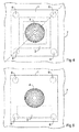
- Figure 4 is a top view of the embodiment according to Figure 1 or 2 .
- a single semiconductor device is mounted on the board 7.
- the hidden contours of the integrated circuit 3 arranged in the semiconductor substrate 1 and of the bump contacts 6 are indicated with broken lines.
- the integrated circuit 3 surrounds the sensor or sensor array 2, which is located opposite the focusing element 4.
- the focusing element 4 is represented as a zone plate, but other structures are not meant to be excluded.
- the dash-dotted diagonal line indicates the position of the cross sections of Figures 1 and 2 .
- Figure 5 is a top view of a further embodiment, which differs from the embodiment according to Figure 4 in the arrangement of the integrated circuit 3.
- the integrated circuit 3 is confined to one side of the sensor or sensor array 2.
- the arrangement of the integrated circuit 3 may be varied according to individual requirements.
- the number and positions of the bump contacts 6 may also vary.
- Figure 6 is a cross section of a semiconductor substrate 1 provided with the sensor or sensor array 2 and the integrated circuit 3 at the main surface 10.
- the semiconductor substrate 1 may be part of a wafer, wherein a plurality of sensors or sensor arrays 2 and a plurality of integrated circuits 3 are produced for a plurality of semiconductor devices.
- the integrated circuit 3 may be produced in a CMOS process, for example.
- a wiring layer 5 can be applied as usual by an arrangement of structured metal layers with dielectric material in between and with vertical electrical connections formed by plugs, for example. The details of the wiring layer 5 are not relevant to the invention and are therefore omitted.
- Figure 7 is a cross section according to Figure 6 for a later stage of the method and shows the etching of the focusing element.
- a mask 14 which may be a resist mask, for instance, is applied to the further main surface 11 opposite the main surface 10.
- the mask 14 has openings in the regions where the trenches forming the focusing element are to be etched.
- the attack of the etching agent is indicated with arrows pointing downwards.
- Figure 8 is a cross section according to Figure 7 after the etching step.
- the etching process is stopped and the mask 14 is removed.
- the optional covering layer 16 and/or the optional bump contacts 6 can be applied.
- the wafer can subsequently be divided into single semiconductor devices, which can be mounted on a board 7 according to Figure 1 .
- Figure 9 is a cross section according to Figure 6 for an embodiment according to Figure 2 .
- a cavity 12 is etched into the main surface 10 of the semiconductor substrate 1, and the sensor or sensor array 2 is arranged in the cavity 12.
- Figure 10 is a cross section according to Figure 9 after the application of a cover 8, which can be a rigid cover like a further substrate or wafer, for example.
- the cover 8 is arranged on or above the main surface 10 and can especially be bonded to the wiring layer 5 by a conventional bonding process, for example.
- a dedicated bonding layer which may be an oxide of the semiconductor material, for instance, may be applied between the wiring layer 5 and the cover 8 for this purpose.
- Figure 10 shows how the cover 8 covers or closes the cavity 12.
- the cover 8 can be provided with recesses 15 for the accomodation of optional bump contacts.
- Figure 11 is a cross section according to Figure 10 for a later stage of the method and shows the etching of the focusing element.
- the elements of the cross section of Figure 11 that correspond to elements of the cross section of Figure 10 are designated with the same reference numerals.
- Figure 11 shows the mask 14 with openings in the regions where the trenches forming the focusing element are to be etched.
- the attack of the etching agent is indicated with arrows pointing downwards.
- Figure 12 is a cross section according to Figure 11 after the etching step.
- the mask 14 has been removed.
- the recesses 15 can be opened by thinning the cover 8 to the level indicated in Figure 12 by the dotted line. This may be performed by grinding the cover 8 back, for example, until the intended thickness is obtained.
- Bump contacts 6 can be arranged in the opened recesses 15. The wafer is then divided into single semiconductor devices, which can be mounted on a board 7 according to Figure 2 .
- Figure 13 is a cross section according to Figure 9 for the embodiment according to Figure 3 .
- a cavity 12 is etched into the main surface 10 of the semiconductor substrate 1, and the sensor or sensor array 2 is arranged in the cavity 12.
- an integrated circuit 3 may be provided in the semiconductor substrate 1 as in the embodiment according to Figure 2 and Figures 9 to 12 .
- Figure 14 is a cross section according to Figure 13 after the application of a cover 8, which is provided with the integrated circuit 13 for the operation of the sensor or sensor array 2.
- the cover 8 is preferably a further substrate or wafer, for example, and the integrated circuit 13 may be arranged opposite the sensor or sensor array 2.
- the cover 8 can be bonded to the wiring layer 5 by any conventional bonding process, for example.
- a dedicated bonding layer which may be an oxide of the semiconductor material, for instance, may be applied between the wiring layer 5 and the cover 8 for this purpose.
- Figure 14 shows how the cover 8 covers or closes the cavity 12.
- the cover 8 can be provided with recesses 15 for the accomodation of bump contacts as in the method according to Figures 9 to 12 .
- Figure 15 is a cross section according to Figure 14 showing the etching of the focusing element.
- the elements of the cross section of Figure 15 that correspond to elements of the cross section of Figure 14 are designated with the same reference numerals.
- Figure 15 shows the mask 14 with openings in the regions where the trenches forming the focusing element are to be etched.
- the attack of the etching agent is indicated with arrows pointing downwards.
- Figure 16 is a cross section according to Figure 15 after the etching step.
- the mask 14 has been removed.
- the recesses 15 can be opened by thinning the cover 8 to the level indicated in Figure 16 by the dotted line as in the method according to Figures 9 to 12 .
- Bump contacts 6 can be arranged in the opened recesses 15.
- the wafer is then divided into single semiconductor devices, which can be mounted on a board 7 according to Figure 3 .
- the described invention allows the fabrication of an integrated focusing element at low cost. It can be employed in many applications to increase the intensity of the radiation impinging on the photosensor and to enhance the performance of the photosensor accordingly.
Landscapes
- Engineering & Computer Science (AREA)
- Microelectronics & Electronic Packaging (AREA)
- Solid State Image Pick-Up Elements (AREA)
Abstract
Description
- The invention relates to wafer-level integration of focusing elements in semiconductor devices like optical sensors. Conventional focusing elements, usually lenses, are discrete elements arranged in the package of the device. They require a lot of space and increase the packaging costs.
-
US 2008/0237761 A1 discloses a system and a method for enhancing light sensitivity of a back-side illumination image sensor. An integrated circuit includes a substrate and an image sensor device comprising at least one transistor formed over a first surface of the substrate and a photosensitive region. A color filter is disposed over an opposite second surface of the substrate. A micro-lens structure is disposed between the second substrate surface and the color filter. -
US 2005/0212132 A1 discloses a chip package including a rigid cover disposed above the active surface of the chip to protect the chip and to enhance the structural strength of the chip package. The rigid cover exposes a plurality of bond pads, which are arranged on the active surface of the chip and carry conductive bumps. The height of the bumps above the surface is larger than the height of the rigid cover. - It is an object of the present invention to disclose a semiconductor device with a focusing element that does not essentially increase the height of the device and is suitable for wafer-level production. It is a further object of the invention to disclose a method of producing such a device. This object is achieved with the semiconductor device according to
claim 1 and with the method of producing a semiconductor device according toclaim 11. Embodiments and variants derive from the dependent claims. - The focusing element is formed within the rear surface of a semiconductor substrate or wafer with integrated components, which can be manufactured at the front side by a standard CMOS process, for instance. The focusing element does not occupy an additional volume of the device. Manufacturing requires only few additional process steps. The invention can be applied to sensor devices conventionally comprising a lens (infrared sensors, for instance) as a compact and cheap way of implementing integrated optics. The performance of many sensor devices (especially photodiodes, for instance) can be enhanced by the focusing element. The proposed invention is especially favourable in conjunction with photosensors that detect radiation in a wavelength range where silicon is transparent (typically infrared radiation).
- The semiconductor device comprises a semiconductor substrate, a sensor or sensor array arranged at a main surface of the substrate, an integrated circuit arranged at or above the main surface, and a focusing element formed within a further main surface of the substrate opposite the main surface. The focusing element is preferably arranged opposite the sensor or sensor array, which may be a photosensor or photodetector or an array of photosensors or photodetectors, for instance.
- The integrated circuit may be arranged in the semiconductor substrate.
- Bump contacts may be arranged at or above the main surface of the semiconductor substrate. The bump contacts can be provided for external electrical connections.
- In an embodiment of the semiconductor device, the focusing element is a diffracting element.
- In a further embodiment, the focusing element is a zone plate comprising a set of radially symmetric Fresnel zones.
- In a further embodiment, a covering layer is present on the focusing element to generate a phase shift zone plate.
- In a further embodiment, the focusing element is a Fresnel lens.
- In a further embodiment, a cover is arranged at or above the main surface to cover the sensor or sensor array or a cavity wherein the sensor or sensor array is arranged, and openings are provided in the cover for the accomodation of bump contacts. The integrated circuit may be arranged in the cover.
- The method of producing a semiconductor device with focusing element comprises arranging a sensor or sensor array at a main surface of a semiconductor substrate, providing an integrated circuit at or above the main surface, and etching a focusing element in a further main surface of the substrate opposite the main surface.
- In a variant of the method, the focusing element is etched in the shape of a zone plate or Fresnel lens.
- In a further variant of the method, a cover is applied to the main surface, before the focusing element is etched. The cover is preferably rigid and can be a further semiconductor substrate or wafer, for instance, which may comprise the integrated circuit. The cover can be provided to cover the sensor or sensor array or a cavity wherein the sensor or sensor array is arranged.
- In a further variant of the method, the cover is provided with openings for bump contacts. The bump contacts can be provided for external electrical connections.
- The following is a detailed description of examples of the semiconductor device and of examples of the method for producing the semiconductor device.
- Figure 1
- is a cross section of an embodiment of the semiconductor device comprising a sensor or sensor array.
- Figure 2
- is a cross section of a further embodiment of the semiconductor device comprising a cover above the sensor or sensor array.
- Figure 3
- is a cross section of a further embodiment of the semiconductor device comprising an integrated circuit arranged in a cover above the sensor or sensor array.
- Figure 4
- is a top view of the embodiment shown in
Figure 1 . - Figure 5
- is a top view of a further embodiment.
- Figure 6
- is a cross section of an intermediate product of a method of producing the semiconductor device.
- Figure 7
- is a cross section according to
Figure 6 in a state during etching of the focusing element. - Figure 8
- is a cross section according to
Figure 7 after the etching process. - Figure 9
- is a cross section of an intermediate product according to
Figure 6 for a further embodiment. - Figure 10
- is a cross section according to
Figure 9 after the application of a cover above the sensor or sensor array. - Figure 11
- is a cross section according to
Figure 10 in a state during etching of the focusing element. - Figure 12
- is a cross section according to
Figure 11 after the etching process. - Figure 13
- is a cross section of an intermediate product according to
Figure 9 for a further embodiment. - Figure 14
- is a cross section according to
Figure 13 after the application of a cover with an integrated circuit. - Figure 15
- is a cross section according to
Figure 14 in a state during etching of the focusing element. - Figure 16
- is a cross section according to
Figure 15 after the etching process. - A focusing
element 4 is arranged within the furthermain surface 11, preferably in a position opposite the sensor orsensor array 2. Awiring layer 5, which may comprise several structured metal layers embedded in intermetal dielectric, can be provided on themain surface 10 as a wiring of theintegrated circuit 3.Optional bump contacts 6, which may be solder balls, for instance, can be arranged on contact areas or pads of thewiring layer 5 to provide external electrical connections. The semiconductor device can be mounted on aboard 7, which may be a printed circuit board (PCB), for instance, by connecting thebump contacts 6 to contact areas or pads of theboard 7. - As the focusing
element 4 is formed within the furthermain surface 11, it does not require any additional volume, and the dimensions of the semiconductor device are therefore extremely small. The focusingelement 4 can be provided with acovering layer 16, which may be an antireflective coating (AR), for instance. The focusingelement 4 can be formed as a diffracting element, in particular as a zone plate comprising a set of radially symmetric Fresnel zones, which are spaced to generate constructive interference at the desired focus. Zone plates and their application to semiconductor devices are known per se. The Fresnel zones of the focusingelement 4 are formed by concentric circular trenches of suitably varying diameters, widths and distances. A coveringlayer 16 of a suitable refractive material can be applied to fill the trenches, as shown inFigure 1 , in order to produce a phase shift zone plate, wherein half wavelength phase delays are created between adjacent ring zones. The elevated regions located between the trenches can be provided with suitably sloping surfaces to form a Fresnel lens, which is also known per se from conventional optical devices and need not be described in detail. - A plurality of semiconductor devices as shown in
Figure 1 can be produced on a wafer. A front side of the wafer is processed to form the sensors and the appertaining electronic circuits, which may especially be CMOS circuits, and the backside of the wafer is etched to produce focusing elements for each of the sensors or sensor arrays. An arrangement of a plurality of sensors in an array can especially be applied for image detection, for example. In this case a plurality of focusing elements may be arranged in a corresponding array opposite the sensors forming the array. -
Figure 2 is a cross section of a further embodiment of the semiconductor device. Elements of the embodiment according toFigure 2 that correspond to elements of the embodiment according toFigure 1 are designated with the same reference numerals. The embodiment according toFigure 2 comprises acover 8 on or above themain surface 10 of thesemiconductor substrate 1. Thecover 8 is preferably rigid and may be a further semiconductor substrate or wafer, for instance. If the sensor orsensor array 2 is arranged in acavity 12 of thesubstrate 1, thecover 8 can be provided to cover or close thecavity 12. If external electrical connections are to be formed by bump contacts,openings 9 are provided in thecover 8 for the accomodation of thebump contacts 6. The height of thebump contacts 6 has to exceed the height of thecover 8 at least slightly to allow thebump contacts 6 to be connected to contact areas or pads of theboard 7. The depth of theopenings 9 is typically not larger than about 100 µm. -
Figure 3 is a cross section of a further embodiment of the semiconductor device. Elements of the embodiment according toFigure 3 that correspond to elements of the embodiment according toFigure 2 are designated with the same reference numerals. The embodiment according toFigure 3 comprises acover 8 on or above themain surface 10 of thesemiconductor substrate 1. Thecover 8 is a further semiconductor substrate of wafer, which is provided with anintegrated circuit 13. Thesubstrate 1 may also comprise anintegrated circuit 3, as in the embodiment according toFigure 2 . Instead, theintegrated circuit 13 of thecover 8 may be the only integrated circuit, as shown in the example ofFigure 3 . If nointegrated circuit 3 is required in thesubstrate 1, the lateral dimensions of the semiconductor device are extremely small. This is especially advantageous if the lateral dimensions of the sensor orsensor array 2 are to be larger than in the examples shown inFigures 1 and 2 . -
Figure 4 is a top view of the embodiment according toFigure 1 or 2 . A single semiconductor device is mounted on theboard 7. The hidden contours of theintegrated circuit 3 arranged in thesemiconductor substrate 1 and of thebump contacts 6 are indicated with broken lines. In the embodiment according toFigure 1 or 2 andFigure 4 , theintegrated circuit 3 surrounds the sensor orsensor array 2, which is located opposite the focusingelement 4. InFigure 4 the focusingelement 4 is represented as a zone plate, but other structures are not meant to be excluded. The dash-dotted diagonal line indicates the position of the cross sections ofFigures 1 and 2 . -
Figure 5 is a top view of a further embodiment, which differs from the embodiment according toFigure 4 in the arrangement of theintegrated circuit 3. In the embodiment according toFigure 5 , theintegrated circuit 3 is confined to one side of the sensor orsensor array 2. The arrangement of theintegrated circuit 3 may be varied according to individual requirements. The number and positions of thebump contacts 6 may also vary. - Methods of producing a semiconductor device with focusing element are described in the following in conjunction with
Figures 6 to 16 , which are cross sections of typical intermediate products of the described methods. -
Figure 6 is a cross section of asemiconductor substrate 1 provided with the sensor orsensor array 2 and theintegrated circuit 3 at themain surface 10. Thesemiconductor substrate 1 may be part of a wafer, wherein a plurality of sensors orsensor arrays 2 and a plurality ofintegrated circuits 3 are produced for a plurality of semiconductor devices. Theintegrated circuit 3 may be produced in a CMOS process, for example. Awiring layer 5 can be applied as usual by an arrangement of structured metal layers with dielectric material in between and with vertical electrical connections formed by plugs, for example. The details of thewiring layer 5 are not relevant to the invention and are therefore omitted. -
Figure 7 is a cross section according toFigure 6 for a later stage of the method and shows the etching of the focusing element. To this end, amask 14, which may be a resist mask, for instance, is applied to the furthermain surface 11 opposite themain surface 10. Themask 14 has openings in the regions where the trenches forming the focusing element are to be etched. InFigure 7 the attack of the etching agent is indicated with arrows pointing downwards. -
Figure 8 is a cross section according toFigure 7 after the etching step. When the trenches of the focusingelement 4 have reached their final depths, the etching process is stopped and themask 14 is removed. Then theoptional covering layer 16 and/or theoptional bump contacts 6 can be applied. The wafer can subsequently be divided into single semiconductor devices, which can be mounted on aboard 7 according toFigure 1 . -
Figure 9 is a cross section according toFigure 6 for an embodiment according toFigure 2 . Acavity 12 is etched into themain surface 10 of thesemiconductor substrate 1, and the sensor orsensor array 2 is arranged in thecavity 12. -
Figure 10 is a cross section according toFigure 9 after the application of acover 8, which can be a rigid cover like a further substrate or wafer, for example. Thecover 8 is arranged on or above themain surface 10 and can especially be bonded to thewiring layer 5 by a conventional bonding process, for example. A dedicated bonding layer, which may be an oxide of the semiconductor material, for instance, may be applied between thewiring layer 5 and thecover 8 for this purpose.Figure 10 shows how thecover 8 covers or closes thecavity 12. Thecover 8 can be provided withrecesses 15 for the accomodation of optional bump contacts. -
Figure 11 is a cross section according toFigure 10 for a later stage of the method and shows the etching of the focusing element. The elements of the cross section ofFigure 11 that correspond to elements of the cross section ofFigure 10 are designated with the same reference numerals.Figure 11 shows themask 14 with openings in the regions where the trenches forming the focusing element are to be etched. The attack of the etching agent is indicated with arrows pointing downwards. -
Figure 12 is a cross section according toFigure 11 after the etching step. Themask 14 has been removed. Therecesses 15 can be opened by thinning thecover 8 to the level indicated inFigure 12 by the dotted line. This may be performed by grinding thecover 8 back, for example, until the intended thickness is obtained.Bump contacts 6 can be arranged in the opened recesses 15. The wafer is then divided into single semiconductor devices, which can be mounted on aboard 7 according toFigure 2 . -
Figure 13 is a cross section according toFigure 9 for the embodiment according toFigure 3 . Acavity 12 is etched into themain surface 10 of thesemiconductor substrate 1, and the sensor orsensor array 2 is arranged in thecavity 12. In this embodiment it is not necessary to integrate an electronic circuit in thesemiconductor substrate 1 for the operation of the sensor orsensor array 2. However, anintegrated circuit 3 may be provided in thesemiconductor substrate 1 as in the embodiment according toFigure 2 andFigures 9 to 12 . -
Figure 14 is a cross section according toFigure 13 after the application of acover 8, which is provided with theintegrated circuit 13 for the operation of the sensor orsensor array 2. Thecover 8 is preferably a further substrate or wafer, for example, and theintegrated circuit 13 may be arranged opposite the sensor orsensor array 2. Thecover 8 can be bonded to thewiring layer 5 by any conventional bonding process, for example. A dedicated bonding layer, which may be an oxide of the semiconductor material, for instance, may be applied between thewiring layer 5 and thecover 8 for this purpose.Figure 14 shows how thecover 8 covers or closes thecavity 12. Thecover 8 can be provided withrecesses 15 for the accomodation of bump contacts as in the method according toFigures 9 to 12 . -
Figure 15 is a cross section according toFigure 14 showing the etching of the focusing element. The elements of the cross section ofFigure 15 that correspond to elements of the cross section ofFigure 14 are designated with the same reference numerals.Figure 15 shows themask 14 with openings in the regions where the trenches forming the focusing element are to be etched. The attack of the etching agent is indicated with arrows pointing downwards. -
Figure 16 is a cross section according toFigure 15 after the etching step. Themask 14 has been removed. Therecesses 15 can be opened by thinning thecover 8 to the level indicated inFigure 16 by the dotted line as in the method according toFigures 9 to 12 .Bump contacts 6 can be arranged in the opened recesses 15. The wafer is then divided into single semiconductor devices, which can be mounted on aboard 7 according toFigure 3 . - The described invention allows the fabrication of an integrated focusing element at low cost. It can be employed in many applications to increase the intensity of the radiation impinging on the photosensor and to enhance the performance of the photosensor accordingly.
-
- 1
- semiconductor substrate
- 2
- sensor or sensor array
- 3
- integrated circuit
- 4
- focusing element
- 5
- wiring layer
- 6
- bump contact
- 7
- board
- 8
- cover
- 9
- opening
- 10
- main surface
- 11
- further main surface
- 12
- cavity
- 13
- integrated circuit
- 14
- mask
- 15
- recess
- 16
- covering layer
Claims (15)
- A semiconductor device, comprising:- a semiconductor substrate (1) with a main surface (10) and a further main surface (11) opposite the main surface (10),- a sensor or sensor array (2) arranged at the main surface (10),- an integrated circuit (3, 13) arranged at or above the main surface (10), and- a focusing element (4) arranged at the further main surface (11),characterized in that- the focusing element (4) is formed within the further main surface (11).
- The semiconductor device of claim 1, wherein the sensor or sensor array (2) is a photosensor or photodetector or an array of photosensors or photodetectors.
- The semiconductor device of claim 1 or 2, wherein the focusing element (4) is a diffracting element.
- The semiconductor device of one of claims 1 to 3, wherein the focusing element (4) is a zone plate comprising a set of radially symmetric Fresnel zones.
- The semiconductor device of claim 4, further comprising: a covering layer (16) on the focusing element (4), the covering layer (16) generating a phase shift zone plate.
- The semiconductor device of claim 1 or 2, wherein the focusing element (4) is a Fresnel lens.
- The semiconductor device of one of claims 1 to 6, further comprising:bump contacts (6) arranged at or above the main surface (10) of the semiconductor substrate (1).
- The semiconductor device of one of claims 1 to 7, wherein the integrated circuit (3) is arranged in the semiconductor substrate (1).
- The semiconductor device of one of claims 1 to 8, further comprising:a cover (8) arranged at or above the main surface (10), andopenings (9) in the cover (8) being provided for bump contacts (6).
- The semiconductor device of claim 9, wherein the integrated circuit (13) is arranged in the cover (8).
- A method of producing a semiconductor device with focusing element, comprising:- arranging a sensor or sensor array (2) at a main surface (10) of a semiconductor substrate (1), and- providing an integrated circuit (3, 13) at or above the main surface (10),characterized in that- a focusing element (4) is etched in a further main surface (11) of the substrate (1) opposite the main surface (10).
- The method of claim 11, wherein the focusing element (4) is etched in the shape of a zone plate or Fresnel lens.
- The method of claim 11 or 12, further comprising:applying a cover (8) to the main surface (10), before the focusing element (4) is etched.
- The method of claim 13, wherein the cover (8) is provided with the integrated circuit (13).
- The method of claim 13 or 14, wherein the cover (8) is provided with openings (9) for bump contacts (6).
Priority Applications (3)
| Application Number | Priority Date | Filing Date | Title |
|---|---|---|---|
| EP14155574.8A EP2908341B1 (en) | 2014-02-18 | 2014-02-18 | Semiconductor device with surface integrated focusing element |
| US15/119,377 US9947711B2 (en) | 2014-02-18 | 2015-02-10 | Semiconductor device with surface integrated focusing element and method of producing a semiconductor device with focusing element |
| PCT/EP2015/052765 WO2015124465A1 (en) | 2014-02-18 | 2015-02-10 | Semiconductor device with surface integrated focusing element and method of producing a semiconductor device with focusing element |
Applications Claiming Priority (1)
| Application Number | Priority Date | Filing Date | Title |
|---|---|---|---|
| EP14155574.8A EP2908341B1 (en) | 2014-02-18 | 2014-02-18 | Semiconductor device with surface integrated focusing element |
Publications (2)
| Publication Number | Publication Date |
|---|---|
| EP2908341A1 true EP2908341A1 (en) | 2015-08-19 |
| EP2908341B1 EP2908341B1 (en) | 2018-07-11 |
Family
ID=50112843
Family Applications (1)
| Application Number | Title | Priority Date | Filing Date |
|---|---|---|---|
| EP14155574.8A Active EP2908341B1 (en) | 2014-02-18 | 2014-02-18 | Semiconductor device with surface integrated focusing element |
Country Status (3)
| Country | Link |
|---|---|
| US (1) | US9947711B2 (en) |
| EP (1) | EP2908341B1 (en) |
| WO (1) | WO2015124465A1 (en) |
Cited By (3)
| Publication number | Priority date | Publication date | Assignee | Title |
|---|---|---|---|---|
| FR3069955A1 (en) * | 2017-08-04 | 2019-02-08 | Stmicroelectronics (Crolles 2) Sas | ELECTRONIC DEVICE FOR ADDITIONAL LAYER IMAGE SENSOR FORMING OPTICAL LENSES |
| CN110021618A (en) * | 2019-04-25 | 2019-07-16 | 德淮半导体有限公司 | A kind of imaging sensor and its manufacturing method |
| CN112331684A (en) * | 2020-11-20 | 2021-02-05 | 联合微电子中心有限责任公司 | Image sensor and forming method thereof |
Families Citing this family (7)
| Publication number | Priority date | Publication date | Assignee | Title |
|---|---|---|---|---|
| EP2908341B1 (en) * | 2014-02-18 | 2018-07-11 | ams AG | Semiconductor device with surface integrated focusing element |
| DE102015004027A1 (en) * | 2015-03-27 | 2016-09-29 | Giesecke & Devrient Gmbh | Security element with effect pigments and an embossed structure and method for its production |
| US10289891B2 (en) | 2016-03-31 | 2019-05-14 | Synaptics Incorpated | Optical biometric sensor having diffractive optical elements |
| CN108381313B (en) * | 2018-04-09 | 2023-08-18 | 奥士康科技股份有限公司 | Substrate inner layer pretreatment device for PCB processing |
| TWI684759B (en) | 2018-12-20 | 2020-02-11 | 新唐科技股份有限公司 | Resistance-integrated gas sensor |
| TWI718765B (en) * | 2019-11-18 | 2021-02-11 | 大陸商廣州立景創新科技有限公司 | Image sensing device |
| US20250194277A1 (en) * | 2023-12-07 | 2025-06-12 | Taiwan Semiconductor Manufacturing Company, Ltd. | Image sensor device with light retention structure |
Citations (6)
| Publication number | Priority date | Publication date | Assignee | Title |
|---|---|---|---|---|
| US20050212132A1 (en) | 2004-03-25 | 2005-09-29 | Min-Chih Hsuan | Chip package and process thereof |
| US20080011937A1 (en) * | 2006-06-30 | 2008-01-17 | Matsushita Electric Industrial Co., Ltd. | Solid-state imaging element and solid-state imaging device |
| US20080237761A1 (en) | 2007-04-02 | 2008-10-02 | Taiwan Semiconductor Manufacturing Company, Ltd. | System and method for enhancing light sensitivity for backside illumination image sensor |
| US20080261346A1 (en) * | 2006-12-29 | 2008-10-23 | Wen-Kun Yang | Semiconductor image device package with die receiving through-hole and method of the same |
| US20130134535A1 (en) * | 2011-11-08 | 2013-05-30 | Victor Lenchenkov | Backside image sensor pixel with silicon microlenses and metal reflector |
| US20130168791A1 (en) * | 2012-01-04 | 2013-07-04 | Vage Oganesian | Quantum Efficiency Back Side Illuminated CMOS Image Sensor And Package, And Method Of Making Same |
Family Cites Families (62)
| Publication number | Priority date | Publication date | Assignee | Title |
|---|---|---|---|---|
| US6012336A (en) * | 1995-09-06 | 2000-01-11 | Sandia Corporation | Capacitance pressure sensor |
| US5900637A (en) * | 1997-05-30 | 1999-05-04 | Massachusetts Institute Of Technology | Maskless lithography using a multiplexed array of fresnel zone plates |
| US6987911B2 (en) * | 2000-03-16 | 2006-01-17 | Lightsmyth Technologies, Inc. | Multimode planar waveguide spectral filter |
| US6890834B2 (en) * | 2001-06-11 | 2005-05-10 | Matsushita Electric Industrial Co., Ltd. | Electronic device and method for manufacturing the same |
| US6894292B2 (en) * | 2002-08-02 | 2005-05-17 | Massachusetts Institute Of Technology | System and method for maskless lithography using an array of sources and an array of focusing elements |
| US20090224351A1 (en) * | 2002-08-27 | 2009-09-10 | E-Phocus, Inc | CMOS sensor with approximately equal potential photodiodes |
| US7279731B1 (en) * | 2006-05-15 | 2007-10-09 | Udt Sensors, Inc. | Edge illuminated photodiodes |
| US7279764B2 (en) * | 2004-06-01 | 2007-10-09 | Micron Technology, Inc. | Silicon-based resonant cavity photodiode for image sensors |
| KR20060077567A (en) * | 2004-12-30 | 2006-07-05 | 동부일렉트로닉스 주식회사 | Image Sensor Using Diffraction Lens |
| KR100670538B1 (en) * | 2004-12-30 | 2007-01-16 | 매그나칩 반도체 유한회사 | Image sensor and its manufacturing method that can improve optical characteristics |
| US7714988B2 (en) * | 2005-02-17 | 2010-05-11 | Massachusetts Institute Of Technology | System and method for absorbance modulation lithography |
| US9068917B1 (en) * | 2006-03-14 | 2015-06-30 | Kla-Tencor Technologies Corp. | Systems and methods for inspection of a specimen |
| WO2008105780A2 (en) * | 2006-05-24 | 2008-09-04 | Pixeloptics, Inc. | Optical rangefinder for an electro-active lens |
| KR100790994B1 (en) * | 2006-08-01 | 2008-01-03 | 삼성전자주식회사 | Image sensor module comprising an image sensor package, a method of manufacturing the same, and an image sensor package |
| DE102007029203A1 (en) * | 2007-06-25 | 2009-01-08 | Giesecke & Devrient Gmbh | security element |
| DE102007029204A1 (en) * | 2007-06-25 | 2009-01-08 | Giesecke & Devrient Gmbh | security element |
| US7800192B2 (en) * | 2008-02-08 | 2010-09-21 | Omnivision Technologies, Inc. | Backside illuminated image sensor having deep light reflective trenches |
| US20100053407A1 (en) * | 2008-02-26 | 2010-03-04 | Tessera, Inc. | Wafer level compliant packages for rear-face illuminated solid state image sensors |
| KR20100028371A (en) * | 2008-09-04 | 2010-03-12 | 주식회사 동부하이텍 | Image sensor and method for manufacturing thereof |
| JP2010245292A (en) * | 2009-04-06 | 2010-10-28 | Panasonic Corp | Optical device, electronic apparatus, and manufacturing method thereof |
| CN101894797B (en) * | 2009-05-20 | 2013-08-28 | 鸿富锦精密工业(深圳)有限公司 | Manufacture method of backside illumination image sensor |
| KR101638183B1 (en) * | 2009-08-11 | 2016-07-11 | 삼성전자주식회사 | Image sensor |
| DE102009049387B4 (en) * | 2009-10-14 | 2016-05-25 | Fraunhofer-Gesellschaft zur Förderung der angewandten Forschung e.V. | Apparatus, image processing apparatus and method for optical imaging |
| US8274101B2 (en) * | 2009-10-20 | 2012-09-25 | Omnivision Technologies, Inc. | CMOS image sensor with heat management structures |
| US8304850B2 (en) * | 2009-12-22 | 2012-11-06 | Texas Instruments Incorporated | Integrated infrared sensors with optical elements, and methods |
| GB201003397D0 (en) * | 2010-03-01 | 2010-04-14 | Rue De Int Ltd | Moire magnification security device |
| US9658053B2 (en) * | 2010-03-09 | 2017-05-23 | Si-Ware Systems | Self calibration for mirror positioning in optical MEMS interferometers |
| WO2011149451A1 (en) * | 2010-05-24 | 2011-12-01 | Omnivision Technologies, Inc. | Dual-sided image sensor |
| WO2011156507A1 (en) * | 2010-06-08 | 2011-12-15 | Edward Hartley Sargent | Stable, sensitive photodetectors and image sensors including circuits, processes, and materials for enhanced imaging performance |
| US8431977B2 (en) * | 2010-06-10 | 2013-04-30 | Megica Corporation | Wafer level processing method and structure to manufacture semiconductor chip |
| US8274124B2 (en) * | 2010-07-07 | 2012-09-25 | United Microelectronics Corp. | Backside illuminated image sensor |
| MTP4307B (en) * | 2010-10-19 | 2012-05-04 | Securency Int Pty Ltd | Security device |
| US8697473B2 (en) * | 2011-01-31 | 2014-04-15 | Aptina Imaging Corporation | Methods for forming backside illuminated image sensors with front side metal redistribution layers |
| KR101095945B1 (en) * | 2011-02-03 | 2011-12-19 | 테쎄라 노쓰 아메리카, 아이엔씨. | Back-illumination sensor package comprising absorbing material for uniformly receiving different wavelengths |
| KR101133154B1 (en) * | 2011-02-03 | 2012-04-06 | 디지털옵틱스 코포레이션 이스트 | Bsi image sensor package with variable-height silicon for even reception of different wavelengths |
| CN102735609A (en) * | 2011-03-31 | 2012-10-17 | 西门子公司 | Body fluid imaging system, method and depth extended imaging device |
| US8604576B2 (en) * | 2011-07-19 | 2013-12-10 | Opitz, Inc. | Low stress cavity package for back side illuminated image sensor, and method of making same |
| KR101948363B1 (en) * | 2011-08-19 | 2019-04-22 | 비쥬얼 피직스 엘엘씨 | Optionally transferable optical system with a reduced thickness |
| US8975715B2 (en) * | 2011-09-14 | 2015-03-10 | Infineon Technologies Ag | Photodetector and method for manufacturing the same |
| KR20130029293A (en) * | 2011-09-14 | 2013-03-22 | 삼성전자주식회사 | Optical input/output device and metho for fabricating the same |
| EP2617353A1 (en) * | 2012-01-22 | 2013-07-24 | Université de Liège | System for an observation of an eye and its surrounding area |
| US9269730B2 (en) * | 2012-02-09 | 2016-02-23 | Semiconductor Components Industries, Llc | Imaging systems with backside isolation trenches |
| US8692344B2 (en) * | 2012-03-16 | 2014-04-08 | Optiz, Inc | Back side illuminated image sensor architecture, and method of making same |
| US20130249031A1 (en) * | 2012-03-22 | 2013-09-26 | Vage Oganesian | Quantum Efficiency Back Side Illuminated CMOS Image Sensor And Package, And Method Of Making Same |
| US9287310B2 (en) * | 2012-04-18 | 2016-03-15 | Taiwan Semiconductor Manufacturing Company, Ltd. | Methods and apparatus for glass removal in CMOS image sensors |
| US8823126B2 (en) * | 2012-05-04 | 2014-09-02 | Hong Kong Applied Science and Technology Research Institute Company Limited | Low cost backside illuminated CMOS image sensor package with high integration |
| JP2014011304A (en) * | 2012-06-29 | 2014-01-20 | Toshiba Corp | Solid-state imaging device |
| WO2014045334A1 (en) * | 2012-09-18 | 2014-03-27 | 富士通株式会社 | Semiconductor light-receiving element, and production method therefor |
| EP2731129A1 (en) * | 2012-11-07 | 2014-05-14 | ams AG | Molded semiconductor sensor device and method of producing the same at a wafer-level |
| EP2802009B1 (en) * | 2013-05-08 | 2021-03-24 | ams AG | Integrated imaging device for infrared radiation and method of production |
| JP6259825B2 (en) * | 2013-06-06 | 2018-01-10 | 浜松ホトニクス株式会社 | ADJUSTING OPTICAL SYSTEM ADJUSTING METHOD, COMPENSATING OPTICAL SYSTEM, AND RECORDING MEDIUM FOR STORING PROGRAM FOR COMPENSATING OPTICAL SYSTEM |
| DE112014002681T5 (en) * | 2013-06-06 | 2016-03-17 | Hamamatsu Photonics K.K. | An angular misalignment method for adaptive optics, an image magnification acquisition method for adaptive optics, and an adaptive optics system |
| CN105637422A (en) * | 2013-08-16 | 2016-06-01 | Asml荷兰有限公司 | Lithographic apparatus, programmable patterning device and lithographic method |
| US20150116527A1 (en) * | 2013-10-31 | 2015-04-30 | Heptagon Micro Optics Pte. Ltd. | Compact array camera modules having an extended field of view from which depth information can be extracted |
| US10542917B2 (en) * | 2014-02-10 | 2020-01-28 | Battelle Memorial Institute | Printed circuit board with embedded sensor |
| US9349770B2 (en) * | 2014-02-11 | 2016-05-24 | Semiconductor Components Industries, Llc | Imaging systems with infrared pixels having increased quantum efficiency |
| EP2908341B1 (en) * | 2014-02-18 | 2018-07-11 | ams AG | Semiconductor device with surface integrated focusing element |
| JP2015170650A (en) * | 2014-03-05 | 2015-09-28 | 株式会社東芝 | Solid-state image pickup device and manufacturing method for the same |
| US9564468B2 (en) * | 2015-03-20 | 2017-02-07 | Taiwan Semiconductor Manufacturing Co., Ltd. | Composite grid structure to reduce crosstalk in back side illumination image sensors |
| US9853076B2 (en) * | 2015-04-16 | 2017-12-26 | Taiwan Semiconductor Manufacturing Co., Ltd. | Stacked grid for more uniform optical input |
| US9991307B2 (en) * | 2015-04-16 | 2018-06-05 | Taiwan Semiconductor Manufacturing Co., Ltd. | Stacked grid design for improved optical performance and isolation |
| WO2017049318A1 (en) * | 2015-09-18 | 2017-03-23 | Synaptics Incorporated | Optical fingerprint sensor package |
-
2014
- 2014-02-18 EP EP14155574.8A patent/EP2908341B1/en active Active
-
2015
- 2015-02-10 WO PCT/EP2015/052765 patent/WO2015124465A1/en not_active Ceased
- 2015-02-10 US US15/119,377 patent/US9947711B2/en active Active
Patent Citations (6)
| Publication number | Priority date | Publication date | Assignee | Title |
|---|---|---|---|---|
| US20050212132A1 (en) | 2004-03-25 | 2005-09-29 | Min-Chih Hsuan | Chip package and process thereof |
| US20080011937A1 (en) * | 2006-06-30 | 2008-01-17 | Matsushita Electric Industrial Co., Ltd. | Solid-state imaging element and solid-state imaging device |
| US20080261346A1 (en) * | 2006-12-29 | 2008-10-23 | Wen-Kun Yang | Semiconductor image device package with die receiving through-hole and method of the same |
| US20080237761A1 (en) | 2007-04-02 | 2008-10-02 | Taiwan Semiconductor Manufacturing Company, Ltd. | System and method for enhancing light sensitivity for backside illumination image sensor |
| US20130134535A1 (en) * | 2011-11-08 | 2013-05-30 | Victor Lenchenkov | Backside image sensor pixel with silicon microlenses and metal reflector |
| US20130168791A1 (en) * | 2012-01-04 | 2013-07-04 | Vage Oganesian | Quantum Efficiency Back Side Illuminated CMOS Image Sensor And Package, And Method Of Making Same |
Cited By (5)
| Publication number | Priority date | Publication date | Assignee | Title |
|---|---|---|---|---|
| FR3069955A1 (en) * | 2017-08-04 | 2019-02-08 | Stmicroelectronics (Crolles 2) Sas | ELECTRONIC DEVICE FOR ADDITIONAL LAYER IMAGE SENSOR FORMING OPTICAL LENSES |
| CN110021618A (en) * | 2019-04-25 | 2019-07-16 | 德淮半导体有限公司 | A kind of imaging sensor and its manufacturing method |
| CN110021618B (en) * | 2019-04-25 | 2022-04-29 | 德淮半导体有限公司 | An image sensor and its manufacturing method |
| CN112331684A (en) * | 2020-11-20 | 2021-02-05 | 联合微电子中心有限责任公司 | Image sensor and forming method thereof |
| CN112331684B (en) * | 2020-11-20 | 2024-02-09 | 联合微电子中心有限责任公司 | Image sensor and method of forming same |
Also Published As
| Publication number | Publication date |
|---|---|
| US20170062504A1 (en) | 2017-03-02 |
| WO2015124465A1 (en) | 2015-08-27 |
| EP2908341B1 (en) | 2018-07-11 |
| US9947711B2 (en) | 2018-04-17 |
Similar Documents
| Publication | Publication Date | Title |
|---|---|---|
| EP2908341B1 (en) | Semiconductor device with surface integrated focusing element | |
| KR102382364B1 (en) | Wafer level image sensor package | |
| EP2802009B1 (en) | Integrated imaging device for infrared radiation and method of production | |
| EP2772939B1 (en) | Semiconductor device for detection of radiation and method of producing a semiconductor device for detection of radiation | |
| KR101761016B1 (en) | Semiconductor device and manufacturing method thereof | |
| US20130168791A1 (en) | Quantum Efficiency Back Side Illuminated CMOS Image Sensor And Package, And Method Of Making Same | |
| KR20130127907A (en) | Bsi image sensor chips with separated color filters and methods for forming the same | |
| CN109564925B (en) | System-on-chip camera with integrated light sensor and method of manufacturing system-on-chip camera | |
| US9881959B2 (en) | Chip package and method of manufacturing the same | |
| JP6599924B2 (en) | Back-lighting solid-state image sensor | |
| US9842946B2 (en) | Semiconductor device comprising an emitter of radiation and a photosensor and appertaining production method | |
| US9059058B2 (en) | Image sensor device with IR filter and related methods | |
| KR20150021659A (en) | Method for manufacturing image sensor | |
| US8318526B2 (en) | Manufacturing method for light-sensing structure | |
| EP3193368B1 (en) | An optoelectronic device with a refractive element and a method of producing such an optoelectronic device | |
| US9373597B2 (en) | Chip package and method thereof | |
| US10132970B2 (en) | Color filter device and forming method thereof | |
| KR100871795B1 (en) | Image sensor and manufacturing method | |
| KR101033387B1 (en) | Image sensor and manufacturing method | |
| KR20100067882A (en) | An image sensor and method for manufacturing the same | |
| HK1196181A (en) | Low profile image sensor package and method | |
| HK1196181B (en) | Low profile image sensor package and method |
Legal Events
| Date | Code | Title | Description |
|---|---|---|---|
| PUAI | Public reference made under article 153(3) epc to a published international application that has entered the european phase |
Free format text: ORIGINAL CODE: 0009012 |
|
| AK | Designated contracting states |
Kind code of ref document: A1 Designated state(s): AL AT BE BG CH CY CZ DE DK EE ES FI FR GB GR HR HU IE IS IT LI LT LU LV MC MK MT NL NO PL PT RO RS SE SI SK SM TR |
|
| AX | Request for extension of the european patent |
Extension state: BA ME |
|
| 17P | Request for examination filed |
Effective date: 20160121 |
|
| RBV | Designated contracting states (corrected) |
Designated state(s): AL AT BE BG CH CY CZ DE DK EE ES FI FR GB GR HR HU IE IS IT LI LT LU LV MC MK MT NL NO PL PT RO RS SE SI SK SM TR |
|
| 17Q | First examination report despatched |
Effective date: 20161018 |
|
| STAA | Information on the status of an ep patent application or granted ep patent |
Free format text: STATUS: EXAMINATION IS IN PROGRESS |
|
| RIC1 | Information provided on ipc code assigned before grant |
Ipc: H01L 31/0203 20140101ALI20180111BHEP Ipc: H01L 27/146 20060101AFI20180111BHEP |
|
| GRAP | Despatch of communication of intention to grant a patent |
Free format text: ORIGINAL CODE: EPIDOSNIGR1 |
|
| STAA | Information on the status of an ep patent application or granted ep patent |
Free format text: STATUS: GRANT OF PATENT IS INTENDED |
|
| INTG | Intention to grant announced |
Effective date: 20180220 |
|
| GRAS | Grant fee paid |
Free format text: ORIGINAL CODE: EPIDOSNIGR3 |
|
| GRAA | (expected) grant |
Free format text: ORIGINAL CODE: 0009210 |
|
| STAA | Information on the status of an ep patent application or granted ep patent |
Free format text: STATUS: THE PATENT HAS BEEN GRANTED |
|
| AK | Designated contracting states |
Kind code of ref document: B1 Designated state(s): AL AT BE BG CH CY CZ DE DK EE ES FI FR GB GR HR HU IE IS IT LI LT LU LV MC MK MT NL NO PL PT RO RS SE SI SK SM TR |
|
| RAP1 | Party data changed (applicant data changed or rights of an application transferred) |
Owner name: AMS AG |
|
| REG | Reference to a national code |
Ref country code: GB Ref legal event code: FG4D |
|
| RIN1 | Information on inventor provided before grant (corrected) |
Inventor name: CARNIELLO, SARA Inventor name: MINIXHOFER, RAINER Inventor name: SCHREMS, MARTIN |
|
| REG | Reference to a national code |
Ref country code: CH Ref legal event code: EP |
|
| REG | Reference to a national code |
Ref country code: AT Ref legal event code: REF Ref document number: 1017804 Country of ref document: AT Kind code of ref document: T Effective date: 20180715 |
|
| REG | Reference to a national code |
Ref country code: IE Ref legal event code: FG4D |
|
| REG | Reference to a national code |
Ref country code: DE Ref legal event code: R096 Ref document number: 602014028147 Country of ref document: DE |
|
| REG | Reference to a national code |
Ref country code: NL Ref legal event code: MP Effective date: 20180711 |
|
| REG | Reference to a national code |
Ref country code: LT Ref legal event code: MG4D |
|
| REG | Reference to a national code |
Ref country code: AT Ref legal event code: MK05 Ref document number: 1017804 Country of ref document: AT Kind code of ref document: T Effective date: 20180711 |
|
| RAP2 | Party data changed (patent owner data changed or rights of a patent transferred) |
Owner name: AMS AG |
|
| PG25 | Lapsed in a contracting state [announced via postgrant information from national office to epo] |
Ref country code: NL Free format text: LAPSE BECAUSE OF FAILURE TO SUBMIT A TRANSLATION OF THE DESCRIPTION OR TO PAY THE FEE WITHIN THE PRESCRIBED TIME-LIMIT Effective date: 20180711 |
|
| PG25 | Lapsed in a contracting state [announced via postgrant information from national office to epo] |
Ref country code: FI Free format text: LAPSE BECAUSE OF FAILURE TO SUBMIT A TRANSLATION OF THE DESCRIPTION OR TO PAY THE FEE WITHIN THE PRESCRIBED TIME-LIMIT Effective date: 20180711 Ref country code: PL Free format text: LAPSE BECAUSE OF FAILURE TO SUBMIT A TRANSLATION OF THE DESCRIPTION OR TO PAY THE FEE WITHIN THE PRESCRIBED TIME-LIMIT Effective date: 20180711 Ref country code: BG Free format text: LAPSE BECAUSE OF FAILURE TO SUBMIT A TRANSLATION OF THE DESCRIPTION OR TO PAY THE FEE WITHIN THE PRESCRIBED TIME-LIMIT Effective date: 20181011 Ref country code: GR Free format text: LAPSE BECAUSE OF FAILURE TO SUBMIT A TRANSLATION OF THE DESCRIPTION OR TO PAY THE FEE WITHIN THE PRESCRIBED TIME-LIMIT Effective date: 20181012 Ref country code: NO Free format text: LAPSE BECAUSE OF FAILURE TO SUBMIT A TRANSLATION OF THE DESCRIPTION OR TO PAY THE FEE WITHIN THE PRESCRIBED TIME-LIMIT Effective date: 20181011 Ref country code: SE Free format text: LAPSE BECAUSE OF FAILURE TO SUBMIT A TRANSLATION OF THE DESCRIPTION OR TO PAY THE FEE WITHIN THE PRESCRIBED TIME-LIMIT Effective date: 20180711 Ref country code: RS Free format text: LAPSE BECAUSE OF FAILURE TO SUBMIT A TRANSLATION OF THE DESCRIPTION OR TO PAY THE FEE WITHIN THE PRESCRIBED TIME-LIMIT Effective date: 20180711 Ref country code: LT Free format text: LAPSE BECAUSE OF FAILURE TO SUBMIT A TRANSLATION OF THE DESCRIPTION OR TO PAY THE FEE WITHIN THE PRESCRIBED TIME-LIMIT Effective date: 20180711 Ref country code: IS Free format text: LAPSE BECAUSE OF FAILURE TO SUBMIT A TRANSLATION OF THE DESCRIPTION OR TO PAY THE FEE WITHIN THE PRESCRIBED TIME-LIMIT Effective date: 20181111 Ref country code: AT Free format text: LAPSE BECAUSE OF FAILURE TO SUBMIT A TRANSLATION OF THE DESCRIPTION OR TO PAY THE FEE WITHIN THE PRESCRIBED TIME-LIMIT Effective date: 20180711 |
|
| PG25 | Lapsed in a contracting state [announced via postgrant information from national office to epo] |
Ref country code: HR Free format text: LAPSE BECAUSE OF FAILURE TO SUBMIT A TRANSLATION OF THE DESCRIPTION OR TO PAY THE FEE WITHIN THE PRESCRIBED TIME-LIMIT Effective date: 20180711 Ref country code: ES Free format text: LAPSE BECAUSE OF FAILURE TO SUBMIT A TRANSLATION OF THE DESCRIPTION OR TO PAY THE FEE WITHIN THE PRESCRIBED TIME-LIMIT Effective date: 20180711 Ref country code: AL Free format text: LAPSE BECAUSE OF FAILURE TO SUBMIT A TRANSLATION OF THE DESCRIPTION OR TO PAY THE FEE WITHIN THE PRESCRIBED TIME-LIMIT Effective date: 20180711 Ref country code: LV Free format text: LAPSE BECAUSE OF FAILURE TO SUBMIT A TRANSLATION OF THE DESCRIPTION OR TO PAY THE FEE WITHIN THE PRESCRIBED TIME-LIMIT Effective date: 20180711 |
|
| REG | Reference to a national code |
Ref country code: DE Ref legal event code: R097 Ref document number: 602014028147 Country of ref document: DE |
|
| PG25 | Lapsed in a contracting state [announced via postgrant information from national office to epo] |
Ref country code: EE Free format text: LAPSE BECAUSE OF FAILURE TO SUBMIT A TRANSLATION OF THE DESCRIPTION OR TO PAY THE FEE WITHIN THE PRESCRIBED TIME-LIMIT Effective date: 20180711 Ref country code: CZ Free format text: LAPSE BECAUSE OF FAILURE TO SUBMIT A TRANSLATION OF THE DESCRIPTION OR TO PAY THE FEE WITHIN THE PRESCRIBED TIME-LIMIT Effective date: 20180711 Ref country code: RO Free format text: LAPSE BECAUSE OF FAILURE TO SUBMIT A TRANSLATION OF THE DESCRIPTION OR TO PAY THE FEE WITHIN THE PRESCRIBED TIME-LIMIT Effective date: 20180711 Ref country code: IT Free format text: LAPSE BECAUSE OF FAILURE TO SUBMIT A TRANSLATION OF THE DESCRIPTION OR TO PAY THE FEE WITHIN THE PRESCRIBED TIME-LIMIT Effective date: 20180711 |
|
| PLBE | No opposition filed within time limit |
Free format text: ORIGINAL CODE: 0009261 |
|
| STAA | Information on the status of an ep patent application or granted ep patent |
Free format text: STATUS: NO OPPOSITION FILED WITHIN TIME LIMIT |
|
| PG25 | Lapsed in a contracting state [announced via postgrant information from national office to epo] |
Ref country code: DK Free format text: LAPSE BECAUSE OF FAILURE TO SUBMIT A TRANSLATION OF THE DESCRIPTION OR TO PAY THE FEE WITHIN THE PRESCRIBED TIME-LIMIT Effective date: 20180711 Ref country code: SK Free format text: LAPSE BECAUSE OF FAILURE TO SUBMIT A TRANSLATION OF THE DESCRIPTION OR TO PAY THE FEE WITHIN THE PRESCRIBED TIME-LIMIT Effective date: 20180711 Ref country code: SM Free format text: LAPSE BECAUSE OF FAILURE TO SUBMIT A TRANSLATION OF THE DESCRIPTION OR TO PAY THE FEE WITHIN THE PRESCRIBED TIME-LIMIT Effective date: 20180711 |
|
| 26N | No opposition filed |
Effective date: 20190412 |
|
| PG25 | Lapsed in a contracting state [announced via postgrant information from national office to epo] |
Ref country code: SI Free format text: LAPSE BECAUSE OF FAILURE TO SUBMIT A TRANSLATION OF THE DESCRIPTION OR TO PAY THE FEE WITHIN THE PRESCRIBED TIME-LIMIT Effective date: 20180711 |
|
| REG | Reference to a national code |
Ref country code: CH Ref legal event code: PL |
|
| GBPC | Gb: european patent ceased through non-payment of renewal fee |
Effective date: 20190218 |
|
| PG25 | Lapsed in a contracting state [announced via postgrant information from national office to epo] |
Ref country code: MC Free format text: LAPSE BECAUSE OF FAILURE TO SUBMIT A TRANSLATION OF THE DESCRIPTION OR TO PAY THE FEE WITHIN THE PRESCRIBED TIME-LIMIT Effective date: 20180711 Ref country code: LU Free format text: LAPSE BECAUSE OF NON-PAYMENT OF DUE FEES Effective date: 20190218 |
|
| REG | Reference to a national code |
Ref country code: BE Ref legal event code: MM Effective date: 20190228 |
|
| REG | Reference to a national code |
Ref country code: IE Ref legal event code: MM4A |
|
| PG25 | Lapsed in a contracting state [announced via postgrant information from national office to epo] |
Ref country code: CH Free format text: LAPSE BECAUSE OF NON-PAYMENT OF DUE FEES Effective date: 20190228 Ref country code: LI Free format text: LAPSE BECAUSE OF NON-PAYMENT OF DUE FEES Effective date: 20190228 |
|
| PG25 | Lapsed in a contracting state [announced via postgrant information from national office to epo] |
Ref country code: IE Free format text: LAPSE BECAUSE OF NON-PAYMENT OF DUE FEES Effective date: 20190218 Ref country code: GB Free format text: LAPSE BECAUSE OF NON-PAYMENT OF DUE FEES Effective date: 20190218 |
|
| PG25 | Lapsed in a contracting state [announced via postgrant information from national office to epo] |
Ref country code: FR Free format text: LAPSE BECAUSE OF NON-PAYMENT OF DUE FEES Effective date: 20190228 Ref country code: BE Free format text: LAPSE BECAUSE OF NON-PAYMENT OF DUE FEES Effective date: 20190228 |
|
| PG25 | Lapsed in a contracting state [announced via postgrant information from national office to epo] |
Ref country code: TR Free format text: LAPSE BECAUSE OF FAILURE TO SUBMIT A TRANSLATION OF THE DESCRIPTION OR TO PAY THE FEE WITHIN THE PRESCRIBED TIME-LIMIT Effective date: 20180711 |
|
| PG25 | Lapsed in a contracting state [announced via postgrant information from national office to epo] |
Ref country code: PT Free format text: LAPSE BECAUSE OF FAILURE TO SUBMIT A TRANSLATION OF THE DESCRIPTION OR TO PAY THE FEE WITHIN THE PRESCRIBED TIME-LIMIT Effective date: 20181111 Ref country code: MT Free format text: LAPSE BECAUSE OF NON-PAYMENT OF DUE FEES Effective date: 20190218 |
|
| PG25 | Lapsed in a contracting state [announced via postgrant information from national office to epo] |
Ref country code: CY Free format text: LAPSE BECAUSE OF FAILURE TO SUBMIT A TRANSLATION OF THE DESCRIPTION OR TO PAY THE FEE WITHIN THE PRESCRIBED TIME-LIMIT Effective date: 20180711 |
|
| PG25 | Lapsed in a contracting state [announced via postgrant information from national office to epo] |
Ref country code: HU Free format text: LAPSE BECAUSE OF FAILURE TO SUBMIT A TRANSLATION OF THE DESCRIPTION OR TO PAY THE FEE WITHIN THE PRESCRIBED TIME-LIMIT; INVALID AB INITIO Effective date: 20140218 |
|
| PG25 | Lapsed in a contracting state [announced via postgrant information from national office to epo] |
Ref country code: MK Free format text: LAPSE BECAUSE OF FAILURE TO SUBMIT A TRANSLATION OF THE DESCRIPTION OR TO PAY THE FEE WITHIN THE PRESCRIBED TIME-LIMIT Effective date: 20180711 |
|
| REG | Reference to a national code |
Ref country code: DE Ref legal event code: R081 Ref document number: 602014028147 Country of ref document: DE Owner name: SAMSUNG ELECTRONICS CO., LTD, SUWON-SI, KR Free format text: FORMER OWNER: AMS AG, PREMSTAETTEN, AT Ref country code: DE Ref legal event code: R082 Ref document number: 602014028147 Country of ref document: DE Representative=s name: HERNANDEZ, YORCK, DIPL.-ING., DE |
|
| REG | Reference to a national code |
Ref country code: DE Ref legal event code: R079 Ref document number: 602014028147 Country of ref document: DE Free format text: PREVIOUS MAIN CLASS: H01L0027146000 Ipc: H10F0039180000 |
|
| PGFP | Annual fee paid to national office [announced via postgrant information from national office to epo] |
Ref country code: DE Payment date: 20260114 Year of fee payment: 13 |