EP2908337A1 - Semiconductor device with a thermally stable bump contact on a TSV and method of producing such a semiconductor device - Google Patents
Semiconductor device with a thermally stable bump contact on a TSV and method of producing such a semiconductor device Download PDFInfo
- Publication number
- EP2908337A1 EP2908337A1 EP14154852.9A EP14154852A EP2908337A1 EP 2908337 A1 EP2908337 A1 EP 2908337A1 EP 14154852 A EP14154852 A EP 14154852A EP 2908337 A1 EP2908337 A1 EP 2908337A1
- Authority
- EP
- European Patent Office
- Prior art keywords
- tsv
- main surface
- under
- semiconductor device
- bump
- Prior art date
- Legal status (The legal status is an assumption and is not a legal conclusion. Google has not performed a legal analysis and makes no representation as to the accuracy of the status listed.)
- Granted
Links
Images


Classifications
-
- H—ELECTRICITY
- H10—SEMICONDUCTOR DEVICES; ELECTRIC SOLID-STATE DEVICES NOT OTHERWISE PROVIDED FOR
- H10W—GENERIC PACKAGES, INTERCONNECTIONS, CONNECTORS OR OTHER CONSTRUCTIONAL DETAILS OF DEVICES COVERED BY CLASS H10
- H10W72/00—Interconnections or connectors in packages
- H10W72/01—Manufacture or treatment
- H10W72/012—Manufacture or treatment of bump connectors, dummy bumps or thermal bumps
-
- H—ELECTRICITY
- H10—SEMICONDUCTOR DEVICES; ELECTRIC SOLID-STATE DEVICES NOT OTHERWISE PROVIDED FOR
- H10W—GENERIC PACKAGES, INTERCONNECTIONS, CONNECTORS OR OTHER CONSTRUCTIONAL DETAILS OF DEVICES COVERED BY CLASS H10
- H10W20/00—Interconnections in chips, wafers or substrates
- H10W20/20—Interconnections within wafers or substrates, e.g. through-silicon vias [TSV]
-
- H—ELECTRICITY
- H10—SEMICONDUCTOR DEVICES; ELECTRIC SOLID-STATE DEVICES NOT OTHERWISE PROVIDED FOR
- H10W—GENERIC PACKAGES, INTERCONNECTIONS, CONNECTORS OR OTHER CONSTRUCTIONAL DETAILS OF DEVICES COVERED BY CLASS H10
- H10W20/00—Interconnections in chips, wafers or substrates
- H10W20/20—Interconnections within wafers or substrates, e.g. through-silicon vias [TSV]
- H10W20/211—Through-semiconductor vias, e.g. TSVs
- H10W20/216—Through-semiconductor vias, e.g. TSVs characterised by dielectric material at least partially filling the via holes, e.g. covering the through-semiconductor vias in the via holes
-
- H—ELECTRICITY
- H10—SEMICONDUCTOR DEVICES; ELECTRIC SOLID-STATE DEVICES NOT OTHERWISE PROVIDED FOR
- H10W—GENERIC PACKAGES, INTERCONNECTIONS, CONNECTORS OR OTHER CONSTRUCTIONAL DETAILS OF DEVICES COVERED BY CLASS H10
- H10W20/00—Interconnections in chips, wafers or substrates
- H10W20/40—Interconnections external to wafers or substrates, e.g. back-end-of-line [BEOL] metallisations or vias connecting to gate electrodes
-
- H—ELECTRICITY
- H10—SEMICONDUCTOR DEVICES; ELECTRIC SOLID-STATE DEVICES NOT OTHERWISE PROVIDED FOR
- H10W—GENERIC PACKAGES, INTERCONNECTIONS, CONNECTORS OR OTHER CONSTRUCTIONAL DETAILS OF DEVICES COVERED BY CLASS H10
- H10W72/00—Interconnections or connectors in packages
- H10W72/20—Bump connectors, e.g. solder bumps or copper pillars; Dummy bumps; Thermal bumps
-
- H—ELECTRICITY
- H10—SEMICONDUCTOR DEVICES; ELECTRIC SOLID-STATE DEVICES NOT OTHERWISE PROVIDED FOR
- H10W—GENERIC PACKAGES, INTERCONNECTIONS, CONNECTORS OR OTHER CONSTRUCTIONAL DETAILS OF DEVICES COVERED BY CLASS H10
- H10W74/00—Encapsulations, e.g. protective coatings
- H10W74/10—Encapsulations, e.g. protective coatings characterised by their shape or disposition
-
- H—ELECTRICITY
- H10—SEMICONDUCTOR DEVICES; ELECTRIC SOLID-STATE DEVICES NOT OTHERWISE PROVIDED FOR
- H10W—GENERIC PACKAGES, INTERCONNECTIONS, CONNECTORS OR OTHER CONSTRUCTIONAL DETAILS OF DEVICES COVERED BY CLASS H10
- H10W74/00—Encapsulations, e.g. protective coatings
- H10W74/10—Encapsulations, e.g. protective coatings characterised by their shape or disposition
- H10W74/131—Encapsulations, e.g. protective coatings characterised by their shape or disposition the semiconductor body being only partially enclosed
-
- H—ELECTRICITY
- H10—SEMICONDUCTOR DEVICES; ELECTRIC SOLID-STATE DEVICES NOT OTHERWISE PROVIDED FOR
- H10W—GENERIC PACKAGES, INTERCONNECTIONS, CONNECTORS OR OTHER CONSTRUCTIONAL DETAILS OF DEVICES COVERED BY CLASS H10
- H10W42/00—Arrangements for protection of devices
- H10W42/121—Arrangements for protection of devices protecting against mechanical damage
-
- H—ELECTRICITY
- H10—SEMICONDUCTOR DEVICES; ELECTRIC SOLID-STATE DEVICES NOT OTHERWISE PROVIDED FOR
- H10W—GENERIC PACKAGES, INTERCONNECTIONS, CONNECTORS OR OTHER CONSTRUCTIONAL DETAILS OF DEVICES COVERED BY CLASS H10
- H10W72/00—Interconnections or connectors in packages
- H10W72/01—Manufacture or treatment
- H10W72/019—Manufacture or treatment of bond pads
- H10W72/01904—Manufacture or treatment of bond pads using temporary auxiliary members, e.g. using sacrificial coatings or handle substrates
-
- H—ELECTRICITY
- H10—SEMICONDUCTOR DEVICES; ELECTRIC SOLID-STATE DEVICES NOT OTHERWISE PROVIDED FOR
- H10W—GENERIC PACKAGES, INTERCONNECTIONS, CONNECTORS OR OTHER CONSTRUCTIONAL DETAILS OF DEVICES COVERED BY CLASS H10
- H10W72/00—Interconnections or connectors in packages
- H10W72/20—Bump connectors, e.g. solder bumps or copper pillars; Dummy bumps; Thermal bumps
- H10W72/241—Dispositions, e.g. layouts
- H10W72/242—Dispositions, e.g. layouts relative to the surface, e.g. recessed, protruding
-
- H—ELECTRICITY
- H10—SEMICONDUCTOR DEVICES; ELECTRIC SOLID-STATE DEVICES NOT OTHERWISE PROVIDED FOR
- H10W—GENERIC PACKAGES, INTERCONNECTIONS, CONNECTORS OR OTHER CONSTRUCTIONAL DETAILS OF DEVICES COVERED BY CLASS H10
- H10W72/00—Interconnections or connectors in packages
- H10W72/20—Bump connectors, e.g. solder bumps or copper pillars; Dummy bumps; Thermal bumps
- H10W72/241—Dispositions, e.g. layouts
- H10W72/244—Dispositions, e.g. layouts relative to underlying supporting features, e.g. bond pads, RDLs or vias
-
- H—ELECTRICITY
- H10—SEMICONDUCTOR DEVICES; ELECTRIC SOLID-STATE DEVICES NOT OTHERWISE PROVIDED FOR
- H10W—GENERIC PACKAGES, INTERCONNECTIONS, CONNECTORS OR OTHER CONSTRUCTIONAL DETAILS OF DEVICES COVERED BY CLASS H10
- H10W72/00—Interconnections or connectors in packages
- H10W72/20—Bump connectors, e.g. solder bumps or copper pillars; Dummy bumps; Thermal bumps
- H10W72/251—Materials
- H10W72/252—Materials comprising solid metals or solid metalloids, e.g. PbSn, Ag or Cu
-
- H—ELECTRICITY
- H10—SEMICONDUCTOR DEVICES; ELECTRIC SOLID-STATE DEVICES NOT OTHERWISE PROVIDED FOR
- H10W—GENERIC PACKAGES, INTERCONNECTIONS, CONNECTORS OR OTHER CONSTRUCTIONAL DETAILS OF DEVICES COVERED BY CLASS H10
- H10W72/00—Interconnections or connectors in packages
- H10W72/20—Bump connectors, e.g. solder bumps or copper pillars; Dummy bumps; Thermal bumps
- H10W72/29—Bond pads specially adapted therefor
-
- H—ELECTRICITY
- H10—SEMICONDUCTOR DEVICES; ELECTRIC SOLID-STATE DEVICES NOT OTHERWISE PROVIDED FOR
- H10W—GENERIC PACKAGES, INTERCONNECTIONS, CONNECTORS OR OTHER CONSTRUCTIONAL DETAILS OF DEVICES COVERED BY CLASS H10
- H10W72/00—Interconnections or connectors in packages
- H10W72/90—Bond pads, in general
-
- H—ELECTRICITY
- H10—SEMICONDUCTOR DEVICES; ELECTRIC SOLID-STATE DEVICES NOT OTHERWISE PROVIDED FOR
- H10W—GENERIC PACKAGES, INTERCONNECTIONS, CONNECTORS OR OTHER CONSTRUCTIONAL DETAILS OF DEVICES COVERED BY CLASS H10
- H10W72/00—Interconnections or connectors in packages
- H10W72/90—Bond pads, in general
- H10W72/921—Structures or relative sizes of bond pads
- H10W72/923—Bond pads having multiple stacked layers
-
- H—ELECTRICITY
- H10—SEMICONDUCTOR DEVICES; ELECTRIC SOLID-STATE DEVICES NOT OTHERWISE PROVIDED FOR
- H10W—GENERIC PACKAGES, INTERCONNECTIONS, CONNECTORS OR OTHER CONSTRUCTIONAL DETAILS OF DEVICES COVERED BY CLASS H10
- H10W72/00—Interconnections or connectors in packages
- H10W72/90—Bond pads, in general
- H10W72/931—Shapes of bond pads
-
- H—ELECTRICITY
- H10—SEMICONDUCTOR DEVICES; ELECTRIC SOLID-STATE DEVICES NOT OTHERWISE PROVIDED FOR
- H10W—GENERIC PACKAGES, INTERCONNECTIONS, CONNECTORS OR OTHER CONSTRUCTIONAL DETAILS OF DEVICES COVERED BY CLASS H10
- H10W72/00—Interconnections or connectors in packages
- H10W72/90—Bond pads, in general
- H10W72/931—Shapes of bond pads
- H10W72/932—Plan-view shape, i.e. in top view
-
- H—ELECTRICITY
- H10—SEMICONDUCTOR DEVICES; ELECTRIC SOLID-STATE DEVICES NOT OTHERWISE PROVIDED FOR
- H10W—GENERIC PACKAGES, INTERCONNECTIONS, CONNECTORS OR OTHER CONSTRUCTIONAL DETAILS OF DEVICES COVERED BY CLASS H10
- H10W72/00—Interconnections or connectors in packages
- H10W72/90—Bond pads, in general
- H10W72/941—Dispositions of bond pads
- H10W72/942—Dispositions of bond pads relative to underlying supporting features, e.g. bond pads, RDLs or vias
-
- H—ELECTRICITY
- H10—SEMICONDUCTOR DEVICES; ELECTRIC SOLID-STATE DEVICES NOT OTHERWISE PROVIDED FOR
- H10W—GENERIC PACKAGES, INTERCONNECTIONS, CONNECTORS OR OTHER CONSTRUCTIONAL DETAILS OF DEVICES COVERED BY CLASS H10
- H10W72/00—Interconnections or connectors in packages
- H10W72/90—Bond pads, in general
- H10W72/951—Materials of bond pads
-
- H—ELECTRICITY
- H10—SEMICONDUCTOR DEVICES; ELECTRIC SOLID-STATE DEVICES NOT OTHERWISE PROVIDED FOR
- H10W—GENERIC PACKAGES, INTERCONNECTIONS, CONNECTORS OR OTHER CONSTRUCTIONAL DETAILS OF DEVICES COVERED BY CLASS H10
- H10W72/00—Interconnections or connectors in packages
- H10W72/90—Bond pads, in general
- H10W72/981—Auxiliary members, e.g. spacers
- H10W72/983—Reinforcing structures, e.g. collars
Definitions
- TSVs through substrate vias
- electrically conductive material in order to reduce thermal stress occurring in the semiconductor substrate.
- Unfilled TSVs may be closed, but the closure is easily damaged when the ambient temperature rises and gas remaining inside the closed TSV expands. This may especially happen during reflow soldering in the manufacturing process.
- US 8,310,058 B2 discloses a semiconductor device comprising a TSV formed in the substrate by deposition of an electrically conductive material.
- An under-bump metallization (UBM) layer is formed on a backside of the substrate in electrical contact with the TSV.
- a solder material is deposited on the UBM layer and reflowed to form a solder bump.
- US 2010/0171209 A1 discloses a semiconductor device formed with stacked semiconductor chips having hollow TSVs, each of which has a tapered portion.
- the chips are connected to one another by solder balls, which comprise a core of a material that has a higher melting point than the surrounding solder material.
- the diameter of the core can be adapted to reduce stress occurring around the electrode.
- US 2013/0040453 A1 discloses a method of forming an UBM layer over a plurality of TSVs. The UBM is connected to a selected portion of the TSVs in common.
- US 2013/0087893 A1 discloses a semiconductor substrate comprising a plurality of TSVs.
- a conductive filler is disposed in each TSV with a void left in the centre to reduce the thermal stress in the semiconductor substrate.
- thermomechanically stable bump contacts on unfilled TSVs It is an object of the present invention to disclose a semiconductor device with thermomechanically stable bump contacts on unfilled TSVs. It is a further object of the invention to disclose a method of producing such a device.
- the semiconductor device comprises a semiconductor substrate with a main surface and a further main surface opposite the main surface, a TSV (through-substrate via) penetrating the substrate from the main surface to the further main surface, a cover layer arranged above the TSV at the main surface, a bump contact arranged on the TSV at the further main surface, and a stress relief feature at the main surface or at the further main surface.
- the stress relief feature is provided to expose the TSV at least partially to the environment, which can be the ambient air, for instance, or any region of the device outside the region occupied by the TSV. The stress relief feature thus provides a communication between the TSV and the environment.
- an under-bump metallization is arranged on the TSV at the further main surface, the bump contact is arranged on the under-bump metallization, and the stress relief feature is formed by the arrangement of the under-bump metallization partially covering a cavity of the TSV without closing it.
- an under-bump metallization is arranged on the TSV at the further main surface, the bump contact is arranged on the under-bump metallization, and a channel in the under-bump metallization forms the stress relief feature.
- the under-bump metallization and the bump contact cover a cavity of the TSV, and the channel connects the cavity with the environment.
- an under-bump metallization is arranged on the TSV at the further main surface, the bump contact is arranged on the under-bump metallization, and a predetermined breaking point in the under-bump metallization forms the stress relief feature.
- the under-bump metallization covers a cavity of the TSV, and the predetermined breaking point is arranged in such a manner that a crack or fissure occurring in the predetermined breaking point connects the cavity with the environment.
- the predetermined breaking point is formed from a material having a lower fracture strength than the under-bump metallization.
- the predetermined breaking point is formed as a striplike region within the under-bump metallization.
- a further embodiment comprises a hole in the cover layer, the hole forming the stress relief feature and connecting a cavity of the TSV with the environment.
- a further embodiment comprises an integrated circuit component in the semiconductor substrate and an appertaining wiring including at least one metal layer arranged in the cover layer.
- the cavity of the TSV can be occupied by a gas or a liquid.
- the TSV can instead be filled with solid material.
- the method of producing embodiments of such a semiconductor device comprises providing a semiconductor substrate with a TSV penetrating the substrate from a main surface to an opposite further main surface, arranging a cover layer above the TSV at the main surface, arranging an under-bump metallization and a bump contact on the TSV at the further main surface, and forming a stress relief feature in the under-bump metallization.
- the stress relief feature is formed by a channel or by a predetermined breaking point.
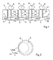
- Figure 1 is a cross section of an embodiment of the semiconductor device comprising a semiconductor substrate 1 with a main surface 10 and a further main surface 11 opposite the main surface 10.
- a cover layer 2 is arranged on the main surface 10.
- the cover layer 2 may be a dielectric layer, for instance, or it may be a wiring layer comprising structured metal layers 4 and interconnections of a wiring embedded in dielectric material. Details of the cover layer 2 are not relevant to the invention.
- the substrate 1 comprises at least one through-substrate via 3, abbreviated TSV, including a metallization 13, which is preferably insulated from the semiconductor material of the substrate 1 by dielectric material forming a sidewall 14, and a central cavity 15, which may be filled with a gas or liquid, for instance.
- TSV 3 is provided as an electrical connection between electrical conductors that are arranged on or above the main surface 10 and further electrical conductors that are arranged on or above the further main surface 11.
- the TSV 3 may especially be provided to connect a terminal of a circuit component 7 that is integrated in the semiconductor substrate 1 with an electrical terminal that is arranged on or above the further main surface 11.
- the semiconductor substrate 1 can instead be a passive component, especially a component used as an interposer for a redistribution of electrical connections, for instance.
- the cover layer 2 closes the cavity 15 of the TSV 3 at the main surface 10.
- a bump contact 6, which may be a solder ball, for instance, is arranged on an under-bump metallization 5, which partially covers the cavity 15 of the TSV 3 at the further main surface 11 and is connected with the metallization 13.
- the cavity 15 is not completely closed by the under-bump metallization 5 and by the bump contact 6, which are placed slightly laterally with respect to a centre of the TSV 3.
- the remaining small opening of the cavity 15 serves as a venting channel.
- Figure 2 is a schematic top view of the bump contact 6 of the embodiment according to Figure 1 .
- the hidden circular contour of the TSV 3, which is cylindrical in this example, and the hidden circular contour of the under-bump metallization 5 are indicated with broken lines.
- the area of the under-bump metallization 5 can be different from a circle, and the TSV 3 need not be cylindrical.
- Figure 2 shows a covered area 15a of the cavity 15 of the TSV 3 where the under-bump metallization 5 is present, and an uncovered area 15b of the cavity 15.
- the bump contact 6 may cover the whole area of the TSV 3 without closing it, as can be seen from Figure 1 . Instead, the perpendicular projection of the bump contact 6 into the plane of the further main surface 11 may not completely cover the area of the TSV 3.
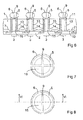
- Figure 3 is a cross section of a further embodiment of the semiconductor device comprising a channel 8 in the layer of the under-bump metallization 5. Elements of the embodiment according to Figure 3 that correspond to elements of the embodiment according to Figure 1 are designated with the same reference numerals.
- the under-bump metallization 5 comprises a channel 8, which provides a connection between the cavity 15 of the TSV 3 and the environment, in particular the ambient air.
- the channel 8 thus functions as a venting channel.
- the bump contact 6 spans the channel 8.
- Figure 4 is a schematic top view of a bump contact 6 of an embodiment comprising a channel 8 within the layer of the under-bump metallization 5.
- the under-bump metallization 5 can be placed centrally with respect to the TSV 3.
- the under-bump metallization 5 has a larger diameter than the cavity 15 of the TSV 3 and overlaps the borders of the cavity 15 as shown in Figure 4 .
- the channel 8 can have any shape, provided that the channel 8 connects the central region of the under-bump metallization 5 with its periphery in such a manner that the cavity 15 communicates with the environment.
- the channel 8 comprises two straight passages, which are arranged along diameters of the under-bump metallization 5 at a right angle. Arrangement and shape of the channel 8 are not restricted to the example represented in Figure 4 .
- the function of the channel 8 is not adversely affected by small residual amounts of solder resist adhering to the sidewalls of the under-bump metallization 5.
- Figure 5 is a schematic top view of the bump contact 6 of the embodiment according to Figure 3 .
- the channel 8 comprises only one straight passage along a diameter of the under-bump metallization 5.
- the position of the cross section of Figure 3 is indicated in Figure 5 by the straight line of dots and dashes.
- Figure 6 is a cross section of a further embodiment of the semiconductor device comprising a predetermined breaking point 9 in the layer of the under-bump metallization 5. Elements of the embodiment according to Figure 6 that correspond to elements of the embodiment according to Figure 3 are designated with the same reference numerals.
- the under-bump metallization 5 is provided with a region comprising a different material forming a predetermined breaking point 9, which is spanned by the bump contact 6.
- the region in question can be similar to the venting channel described above in conjunction with Figures 3 to 5 .
- the channel is not left open but filled with a material that has a lower fracture strength than the material of the under-bump metallization 5.
- the predetermined breaking point 9 thus serves as a pressure relief valve protecting the TSV 3.
- Figure 7 is a schematic top view of a bump contact 6 of an embodiment comprising a predetermined breaking point 9 within the layer of the under-bump metallization 5.
- the under-bump metallization 5 can be placed centrally with respect to the location of the TSV 3.
- the under-bump metallization 5 has a larger diameter than the cavity 15 of the TSV 3 and overlaps the borders of the cavity 15 as shown in Figure 7 .
- the region of the predetermined breaking point 9 can have any shape, provided that it connects the central region of the under-bump metallization 5 with its periphery in such a manner that cracks or fissures generated in the predetermined breaking point 9 can form a channel venting the cavity 15.
- the predetermined breaking point 9 comprises two straight striplike regions arranged along diameters of the under-bump metallization 5 at a right angle.
- Figure 8 is a schematic top view of the bump contact 6 of the embodiment according to Figure 6 .
- the predetermined breaking point 9 comprises only one straight striplike region arranged along a diameter of the under-bump metallization 5.
- the position of the cross section of Figure 6 is indicated in Figure 8 by the straight line of dots and dashes.
- FIG. 9 is a cross section of a further embodiment of the semiconductor device comprising a TSV 3 with a venting hole 12 in the cover layer 2 on the main surface 10 of the semiconductor substrate 1.
- Elements of the embodiment according to Figure 9 that correspond to elements of the embodiment according to Figure 6 are designated with the same reference numerals.
- the hole 12 penetrating the cover layer 2 connects the cavity 15 of the TSV 3 with the environment, in particular with the ambient air.
- the TSV 3 is thus almost completely closed, and the bump contact 6 is allowed to cover the TSV 3 completely at the further main surface 11. Contamination of the TSV 3 by underfill material or the like entering the cavity 15 can thus be prevented, and stress owing to an extension of gas inside the cavity 15 is prevented at the same time.
- Figure 10 is a schematic top view of the bump contact 6 of the embodiment according to Figure 9 .
- the outline of the position of the hole 12 is indicated with a circular broken line in the centre of the area representing the cavity 15.
- the hole 12 can be arranged at any other suitable position in the area of the cavity 15, and there may be two or more such holes 12 in the cover layer 2 for the same TSV 3.
- the invention has the advantage that fractures in the metallization of the TSV, in the material of the bump contacts or in the under-bump metallization are avoided even under changing ambient temperatures. If expanding liquids or gases enclosed within the TSV can escape through a venting channel, the risk of damages of bump contacts allowing small lateral dimensions of the semiconductor device is reduced. Thus the bump contacts are thermally stable. Underfill material, which may be employed to fix the device on a printed circuit board, is less likely to contaminate the interior of the TSV.
- the invention is especially favourable for unfilled TSVs, i. e., for TSVs that are not filled with solid material but may contain a gas or a liquid, but it can also be employed for TSVs filled with a metal or dielectric material. In each case an effective stress relief is provided at the interface between the under-bump metallization and the bump contact and/or the filling material.
Landscapes
- Internal Circuitry In Semiconductor Integrated Circuit Devices (AREA)
- Engineering & Computer Science (AREA)
- Manufacturing & Machinery (AREA)
Abstract

Description
- The increasing density of components that are integrated in semiconductor devices requires an increasing density of electrical interconnections between these components. This may be achieved with the aid of through substrate vias (TSVs), which have typical diameters in the range from 2 µm to 100 µm. It may be preferable not to fill the TSVs with electrically conductive material in order to reduce thermal stress occurring in the semiconductor substrate. Unfilled TSVs may be closed, but the closure is easily damaged when the ambient temperature rises and gas remaining inside the closed TSV expands. This may especially happen during reflow soldering in the manufacturing process.
-
US 8,310,058 B2 discloses a semiconductor device comprising a TSV formed in the substrate by deposition of an electrically conductive material. An under-bump metallization (UBM) layer is formed on a backside of the substrate in electrical contact with the TSV. A solder material is deposited on the UBM layer and reflowed to form a solder bump. -
US 2010/0171209 A1 discloses a semiconductor device formed with stacked semiconductor chips having hollow TSVs, each of which has a tapered portion. The chips are connected to one another by solder balls, which comprise a core of a material that has a higher melting point than the surrounding solder material. The diameter of the core can be adapted to reduce stress occurring around the electrode.US 2013/0040453 A1 discloses a method of forming an UBM layer over a plurality of TSVs. The UBM is connected to a selected portion of the TSVs in common. -
US 2013/0087893 A1 discloses a semiconductor substrate comprising a plurality of TSVs. A conductive filler is disposed in each TSV with a void left in the centre to reduce the thermal stress in the semiconductor substrate. - It is an object of the present invention to disclose a semiconductor device with thermomechanically stable bump contacts on unfilled TSVs. It is a further object of the invention to disclose a method of producing such a device.
- This object is achieved with the semiconductor device according to
claim 1 and with the method of producing a semiconductor device according toclaim 13. Embodiments and variants derive from the dependent claims. - The semiconductor device comprises a semiconductor substrate with a main surface and a further main surface opposite the main surface, a TSV (through-substrate via) penetrating the substrate from the main surface to the further main surface, a cover layer arranged above the TSV at the main surface, a bump contact arranged on the TSV at the further main surface, and a stress relief feature at the main surface or at the further main surface. The stress relief feature is provided to expose the TSV at least partially to the environment, which can be the ambient air, for instance, or any region of the device outside the region occupied by the TSV. The stress relief feature thus provides a communication between the TSV and the environment.
- In an embodiment of the semiconductor device, an under-bump metallization is arranged on the TSV at the further main surface, the bump contact is arranged on the under-bump metallization, and the stress relief feature is formed by the arrangement of the under-bump metallization partially covering a cavity of the TSV without closing it.
- In a further embodiment, an under-bump metallization is arranged on the TSV at the further main surface, the bump contact is arranged on the under-bump metallization, and a channel in the under-bump metallization forms the stress relief feature.
- In a further embodiment, the under-bump metallization and the bump contact cover a cavity of the TSV, and the channel connects the cavity with the environment.
- In a further embodiment, an under-bump metallization is arranged on the TSV at the further main surface, the bump contact is arranged on the under-bump metallization, and a predetermined breaking point in the under-bump metallization forms the stress relief feature.
- In a further embodiment, the under-bump metallization covers a cavity of the TSV, and the predetermined breaking point is arranged in such a manner that a crack or fissure occurring in the predetermined breaking point connects the cavity with the environment.
- In a further embodiment, the predetermined breaking point is formed from a material having a lower fracture strength than the under-bump metallization.
- In a further embodiment, the predetermined breaking point is formed as a striplike region within the under-bump metallization.
- A further embodiment comprises a hole in the cover layer, the hole forming the stress relief feature and connecting a cavity of the TSV with the environment.
- A further embodiment comprises an integrated circuit component in the semiconductor substrate and an appertaining wiring including at least one metal layer arranged in the cover layer.
- The cavity of the TSV can be occupied by a gas or a liquid. The TSV can instead be filled with solid material.
- The method of producing embodiments of such a semiconductor device comprises providing a semiconductor substrate with a TSV penetrating the substrate from a main surface to an opposite further main surface, arranging a cover layer above the TSV at the main surface, arranging an under-bump metallization and a bump contact on the TSV at the further main surface, and forming a stress relief feature in the under-bump metallization.
- In variants of the method the stress relief feature is formed by a channel or by a predetermined breaking point.
- The following is a detailed description of examples of the semiconductor device and of examples of the method for producing the semiconductor device.
- Figure 1
- is a cross section of an embodiment of the semiconductor device.
- Figure 2
- is a schematic top view of a bump contact of the embodiment according to
Figure 1 . - Figure 3
- is a cross section of a further embodiment of the semiconductor device comprising a venting channel.
- Figure 4
- is a schematic top view of a bump contact of an embodiment comprising a venting channel.
- Figure 5
- is a schematic top view of a bump contact of the embodiment according to
Figure 3 . - Figure 6
- is a cross section of a further embodiment of the semiconductor device comprising a predetermined breaking point.
- Figure 7
- is a schematic top view of a bump contact of an embodiment comprising a predetermined breaking point.
- Figure 8
- is a schematic top view of a bump contact of the embodiment according to
Figure 6 . - Figure 9
- is a cross section of a further embodiment of the semiconductor device comprising a pierced cover layer on the TSV.
- Figure 10
- is a schematic top view of a bump contact of the embodiment according to
Figure 9 . -
Figure 1 is a cross section of an embodiment of the semiconductor device comprising asemiconductor substrate 1 with amain surface 10 and a furthermain surface 11 opposite themain surface 10. Acover layer 2 is arranged on themain surface 10. Thecover layer 2 may be a dielectric layer, for instance, or it may be a wiring layer comprising structuredmetal layers 4 and interconnections of a wiring embedded in dielectric material. Details of thecover layer 2 are not relevant to the invention. - The
substrate 1 comprises at least one through-substrate via 3, abbreviated TSV, including ametallization 13, which is preferably insulated from the semiconductor material of thesubstrate 1 by dielectric material forming asidewall 14, and acentral cavity 15, which may be filled with a gas or liquid, for instance. The TSV 3 is provided as an electrical connection between electrical conductors that are arranged on or above themain surface 10 and further electrical conductors that are arranged on or above the furthermain surface 11. The TSV 3 may especially be provided to connect a terminal of acircuit component 7 that is integrated in thesemiconductor substrate 1 with an electrical terminal that is arranged on or above the furthermain surface 11. Thesemiconductor substrate 1 can instead be a passive component, especially a component used as an interposer for a redistribution of electrical connections, for instance. - The
cover layer 2 closes thecavity 15 of the TSV 3 at themain surface 10. Abump contact 6, which may be a solder ball, for instance, is arranged on an under-bump metallization 5, which partially covers thecavity 15 of theTSV 3 at the furthermain surface 11 and is connected with themetallization 13. Thecavity 15 is not completely closed by the under-bump metallization 5 and by thebump contact 6, which are placed slightly laterally with respect to a centre of theTSV 3. The remaining small opening of thecavity 15 serves as a venting channel. -
Figure 2 is a schematic top view of thebump contact 6 of the embodiment according toFigure 1 . The hidden circular contour of theTSV 3, which is cylindrical in this example, and the hidden circular contour of the under-bump metallization 5 are indicated with broken lines. In further embodiments, the area of the under-bump metallization 5 can be different from a circle, and theTSV 3 need not be cylindrical.Figure 2 shows a coveredarea 15a of thecavity 15 of theTSV 3 where the under-bump metallization 5 is present, and an uncoveredarea 15b of thecavity 15. Thebump contact 6 may cover the whole area of theTSV 3 without closing it, as can be seen fromFigure 1 . Instead, the perpendicular projection of thebump contact 6 into the plane of the furthermain surface 11 may not completely cover the area of theTSV 3. -
Figure 3 is a cross section of a further embodiment of the semiconductor device comprising achannel 8 in the layer of the under-bump metallization 5. Elements of the embodiment according toFigure 3 that correspond to elements of the embodiment according toFigure 1 are designated with the same reference numerals. In the embodiment according toFigure 3 , the under-bump metallization 5 comprises achannel 8, which provides a connection between thecavity 15 of theTSV 3 and the environment, in particular the ambient air. Thechannel 8 thus functions as a venting channel. Thebump contact 6 spans thechannel 8. -
Figure 4 is a schematic top view of abump contact 6 of an embodiment comprising achannel 8 within the layer of the under-bump metallization 5. In this embodiment the under-bump metallization 5 can be placed centrally with respect to theTSV 3. The under-bump metallization 5 has a larger diameter than thecavity 15 of theTSV 3 and overlaps the borders of thecavity 15 as shown inFigure 4 . Thechannel 8 can have any shape, provided that thechannel 8 connects the central region of the under-bump metallization 5 with its periphery in such a manner that thecavity 15 communicates with the environment. In the embodiment according toFigure 4 , thechannel 8 comprises two straight passages, which are arranged along diameters of the under-bump metallization 5 at a right angle. Arrangement and shape of thechannel 8 are not restricted to the example represented inFigure 4 . The function of thechannel 8 is not adversely affected by small residual amounts of solder resist adhering to the sidewalls of the under-bump metallization 5. -
Figure 5 is a schematic top view of thebump contact 6 of the embodiment according toFigure 3 . Here thechannel 8 comprises only one straight passage along a diameter of the under-bump metallization 5. The position of the cross section ofFigure 3 is indicated inFigure 5 by the straight line of dots and dashes. -
Figure 6 is a cross section of a further embodiment of the semiconductor device comprising apredetermined breaking point 9 in the layer of the under-bump metallization 5. Elements of the embodiment according toFigure 6 that correspond to elements of the embodiment according toFigure 3 are designated with the same reference numerals. In the embodiment according toFigure 6 , the under-bump metallization 5 is provided with a region comprising a different material forming apredetermined breaking point 9, which is spanned by thebump contact 6. The region in question can be similar to the venting channel described above in conjunction withFigures 3 to 5 . The channel is not left open but filled with a material that has a lower fracture strength than the material of the under-bump metallization 5. Stress occurring in the layer of the under-bump metallization 5 is therefore liable to cause cracks or fissures in the material of thepredetermined breaking point 9, so that a channel venting thecavity 15 is produced. Thepredetermined breaking point 9 thus serves as a pressure relief valve protecting theTSV 3. -
Figure 7 is a schematic top view of abump contact 6 of an embodiment comprising apredetermined breaking point 9 within the layer of the under-bump metallization 5. In this embodiment the under-bump metallization 5 can be placed centrally with respect to the location of theTSV 3. The under-bump metallization 5 has a larger diameter than thecavity 15 of theTSV 3 and overlaps the borders of thecavity 15 as shown inFigure 7 . The region of thepredetermined breaking point 9 can have any shape, provided that it connects the central region of the under-bump metallization 5 with its periphery in such a manner that cracks or fissures generated in thepredetermined breaking point 9 can form a channel venting thecavity 15. In the embodiment according toFigure 7 , thepredetermined breaking point 9 comprises two straight striplike regions arranged along diameters of the under-bump metallization 5 at a right angle. -
Figure 8 is a schematic top view of thebump contact 6 of the embodiment according toFigure 6 . Thepredetermined breaking point 9 comprises only one straight striplike region arranged along a diameter of the under-bump metallization 5. The position of the cross section ofFigure 6 is indicated inFigure 8 by the straight line of dots and dashes. -
Figure 9 is a cross section of a further embodiment of the semiconductor device comprising aTSV 3 with a ventinghole 12 in thecover layer 2 on themain surface 10 of thesemiconductor substrate 1. Elements of the embodiment according toFigure 9 that correspond to elements of the embodiment according toFigure 6 are designated with the same reference numerals. In the embodiment according toFigure 9 , thehole 12 penetrating thecover layer 2 connects thecavity 15 of theTSV 3 with the environment, in particular with the ambient air. TheTSV 3 is thus almost completely closed, and thebump contact 6 is allowed to cover theTSV 3 completely at the furthermain surface 11. Contamination of theTSV 3 by underfill material or the like entering thecavity 15 can thus be prevented, and stress owing to an extension of gas inside thecavity 15 is prevented at the same time. -
Figure 10 is a schematic top view of thebump contact 6 of the embodiment according toFigure 9 . The outline of the position of thehole 12 is indicated with a circular broken line in the centre of the area representing thecavity 15. Thehole 12 can be arranged at any other suitable position in the area of thecavity 15, and there may be two or moresuch holes 12 in thecover layer 2 for thesame TSV 3. - The invention has the advantage that fractures in the metallization of the TSV, in the material of the bump contacts or in the under-bump metallization are avoided even under changing ambient temperatures. If expanding liquids or gases enclosed within the TSV can escape through a venting channel, the risk of damages of bump contacts allowing small lateral dimensions of the semiconductor device is reduced. Thus the bump contacts are thermally stable. Underfill material, which may be employed to fix the device on a printed circuit board, is less likely to contaminate the interior of the TSV. The invention is especially favourable for unfilled TSVs, i. e., for TSVs that are not filled with solid material but may contain a gas or a liquid, but it can also be employed for TSVs filled with a metal or dielectric material. In each case an effective stress relief is provided at the interface between the under-bump metallization and the bump contact and/or the filling material.
-
- 1
- semiconductor substrate
- 2
- cover layer
- 3
- TSV
- 4
- metal layer
- 5
- under-bump metallization
- 6
- bump contact
- 7
- integrated circuit component
- 8
- channel
- 9
- predetermined breaking point
- 10
- main surface
- 11
- further main surface
- 12
- hole
- 13
- metallization
- 14
- sidewall
- 15
- cavity
- 15a
- covered area of the cavity
- 15b
- uncovered area of the cavity
Claims (15)
- A semiconductor device, comprising:- a semiconductor substrate (1) having a main surface (10) and a further main surface (11) opposite the main surface (10),- a TSV (3) penetrating the substrate (1) from the main surface (10) to the further main surface (11),- a cover layer (2) arranged above the TSV (3) at the main surface (10), and- a bump contact (6) arranged on the TSV (3) at the further main surface (11),
characterized in that- a stress relief feature is present at the main surface (10) or at the further main surface (11), the stress relief feature providing a communication between the TSV (3) and an environment. - The semiconductor device of claim 1, further comprising:- an under-bump metallization (5) arranged on the TSV (3) at the further main surface (11), the bump contact (6) being arranged on the under-bump metallization (5), and- a cavity (15) of the TSV (3), wherein- the stress relief feature is formed by the arrangement of the under-bump metallization (5) partially covering the cavity (15) without closing it.
- The semiconductor device of claim 1, further comprising:- an under-bump metallization (5) arranged on the TSV (3) at the further main surface (11), the bump contact (6) being arranged on the under-bump metallization (5), and- a channel (8) in the under-bump metallization (5), the channel (8) forming the stress relief feature.
- The semiconductor device of claim 3, further comprising:- a cavity (15) of the TSV (3),- the under-bump metallization (5) and the bump contact (6) covering the cavity (15), and- the channel (8) connecting the cavity (15) with the environment.
- The semiconductor device of claim 1, further comprising:- an under-bump metallization (5) arranged on the TSV (3) at the further main surface (11), the bump contact (6) being arranged on the under-bump metallization (5), and- a predetermined breaking point (9) in the under-bump metallization (5), the predetermined breaking point (9) forming the stress relief feature.
- The semiconductor device of claim 5, further comprising:- a cavity (15) of the TSV (3),- the under-bump metallization (5) covering the cavity (15), and- the predetermined breaking point (9) being arranged in such a manner that a crack or fissure occurring in the predetermined breaking point (9) connects the cavity (15) with the environment.
- The semiconductor device of claim 5 or 6, wherein the predetermined breaking point (9) is formed from a material having a lower fracture strength than the under-bump metallization (5).
- The semiconductor device of one of claims 5 to 7, wherein the predetermined breaking point (9) is formed as a striplike region within the under-bump metallization (5).
- The semiconductor device of claim 1, further comprising:- a hole (12) in the cover layer (2), the hole (12) forming the stress relief feature, and- a cavity (15) of the TSV (3), the hole (12) connecting the cavity (15) with the environment.
- The semiconductor device of claim 9, further comprising:an integrated circuit component (7) in the semiconductor substrate (1), the integrated circuit component (7) being provided with a wiring including at least one metal layer (4) arranged in the cover layer (2).
- The semiconductor device of one of claims 2 to 10,
wherein the cavity (15) of the TSV (3) is filled with a gas or a liquid. - The semiconductor device of one of claims 1 to 8, wherein the TSV (3) is filled with solid material.
- A method of producing a semiconductor device, comprising:- providing a semiconductor substrate (1) with a TSV (3) penetrating the substrate (1) from a main surface (10) to an opposite further main surface (11),- arranging a cover layer (2) above the TSV (3) at the main surface (10), and- arranging an under-bump metallization (5) and a bump contact (6) on the TSV (3) at the further main surface (11),
characterized in that- a stress relief feature is formed in the under-bump metallization (5). - The method of claim 13, wherein the stress relief feature is formed by a channel (8).
- The method of claim 13, wherein the stress relief feature is formed by a predetermined breaking point (9).
Priority Applications (3)
| Application Number | Priority Date | Filing Date | Title |
|---|---|---|---|
| EP14154852.9A EP2908337B1 (en) | 2014-02-12 | 2014-02-12 | Semiconductor device with a thermally stable bump contact on a TSV and method of producing such a semiconductor device |
| US15/118,469 US10217715B2 (en) | 2014-02-12 | 2015-02-09 | Semiconductor device with a bump contact on a TSV comprising a cavity and method of producing such a semiconductor device |
| PCT/EP2015/052647 WO2015121199A2 (en) | 2014-02-12 | 2015-02-09 | Semiconductor device with a bump contact on a tsv comprising a cavity and method of producing such a semiconductor device |
Applications Claiming Priority (1)
| Application Number | Priority Date | Filing Date | Title |
|---|---|---|---|
| EP14154852.9A EP2908337B1 (en) | 2014-02-12 | 2014-02-12 | Semiconductor device with a thermally stable bump contact on a TSV and method of producing such a semiconductor device |
Publications (2)
| Publication Number | Publication Date |
|---|---|
| EP2908337A1 true EP2908337A1 (en) | 2015-08-19 |
| EP2908337B1 EP2908337B1 (en) | 2025-11-12 |
Family
ID=50071537
Family Applications (1)
| Application Number | Title | Priority Date | Filing Date |
|---|---|---|---|
| EP14154852.9A Active EP2908337B1 (en) | 2014-02-12 | 2014-02-12 | Semiconductor device with a thermally stable bump contact on a TSV and method of producing such a semiconductor device |
Country Status (3)
| Country | Link |
|---|---|
| US (1) | US10217715B2 (en) |
| EP (1) | EP2908337B1 (en) |
| WO (1) | WO2015121199A2 (en) |
Cited By (2)
| Publication number | Priority date | Publication date | Assignee | Title |
|---|---|---|---|---|
| CN108550556A (en) * | 2018-05-31 | 2018-09-18 | 京东方科技集团股份有限公司 | Protective film and its display panel for flexible substrate |
| US11139207B2 (en) | 2017-10-12 | 2021-10-05 | Ams Ag | Method for manufacturing a semiconductor device and semiconductor device |
Families Citing this family (4)
| Publication number | Priority date | Publication date | Assignee | Title |
|---|---|---|---|---|
| US10957626B2 (en) | 2017-12-19 | 2021-03-23 | Thermo Electron Scientific Instruments Llc | Sensor device with carbon nanotube sensor positioned on first and second substrates |
| KR102450580B1 (en) | 2017-12-22 | 2022-10-07 | 삼성전자주식회사 | Semiconductor Device having a Structure for Insulating Layer under Metal Line |
| KR102775522B1 (en) * | 2020-03-12 | 2025-03-06 | 에스케이하이닉스 주식회사 | Stacked type semiconductor device and manufacturing method of the same |
| KR102952543B1 (en) | 2021-07-08 | 2026-04-14 | 삼성전자주식회사 | Substrate structure connecting based on solder ball and elastic body |
Citations (10)
| Publication number | Priority date | Publication date | Assignee | Title |
|---|---|---|---|---|
| US20090243047A1 (en) * | 2008-04-01 | 2009-10-01 | Andreas Wolter | Semiconductor Device With an Interconnect Element and Method for Manufacture |
| DE102009012643A1 (en) * | 2008-03-10 | 2009-10-01 | Fraunhofer-Gesellschaft zur Förderung der angewandten Forschung e.V. | Connecting structure for connecting electronic component i.e. semiconductor chip, and/or substrate carrier on organic printed circuit board, has contact elements at which material of component or carrier is removed for forming free area |
| US20100171209A1 (en) | 2009-01-05 | 2010-07-08 | Hitachi Metals, Ltd. | Semiconductor device and method for manufacturing the same |
| US20110272801A1 (en) * | 2010-05-06 | 2011-11-10 | Stmicroelectronics S.A. | Semiconductor device with connection pads provided with inserts |
| US8310058B2 (en) | 2007-11-29 | 2012-11-13 | Stats Chippac, Ltd. | Semiconductor device and method for forming passive circuit elements with through silicon vias to backside interconnect structures |
| US20130026645A1 (en) * | 2011-07-29 | 2013-01-31 | Tessera, Inc. | Low stress vias |
| US20130040453A1 (en) | 2008-08-05 | 2013-02-14 | Taiwan Semiconductor Manufacturing Company, Ltd. | Through Silicon Via Layout |
| US20130087893A1 (en) | 2011-10-07 | 2013-04-11 | Newport Fab, Llc Dba Jazz Semiconductor | Through Silicon Via Structure, Method of Formation, and Integration in Semiconductor Substrate |
| US20130249098A1 (en) * | 2011-06-01 | 2013-09-26 | Texas Instruments Incorporated | Protective layer for protecting tsv tips during thermo-compressive bonding |
| US20130328209A1 (en) * | 2010-02-12 | 2013-12-12 | Agency For Science, Technology And Research | Stack Arrangement |
Family Cites Families (4)
| Publication number | Priority date | Publication date | Assignee | Title |
|---|---|---|---|---|
| US6380060B1 (en) * | 2000-03-08 | 2002-04-30 | Tessera, Inc. | Off-center solder ball attach and methods therefor |
| US6622905B2 (en) | 2000-12-29 | 2003-09-23 | Intel Corporation | Design and assembly methodology for reducing bridging in bonding electronic components to pads connected to vias |
| EP2620978B1 (en) | 2012-01-25 | 2019-07-24 | austriamicrosystems AG | Semiconductor device with internal substrate contact and method of production |
| KR102064863B1 (en) * | 2013-08-29 | 2020-01-10 | 삼성전자주식회사 | Method of fabricating Semiconductor Devices Having TSV |
-
2014
- 2014-02-12 EP EP14154852.9A patent/EP2908337B1/en active Active
-
2015
- 2015-02-09 US US15/118,469 patent/US10217715B2/en active Active
- 2015-02-09 WO PCT/EP2015/052647 patent/WO2015121199A2/en not_active Ceased
Patent Citations (10)
| Publication number | Priority date | Publication date | Assignee | Title |
|---|---|---|---|---|
| US8310058B2 (en) | 2007-11-29 | 2012-11-13 | Stats Chippac, Ltd. | Semiconductor device and method for forming passive circuit elements with through silicon vias to backside interconnect structures |
| DE102009012643A1 (en) * | 2008-03-10 | 2009-10-01 | Fraunhofer-Gesellschaft zur Förderung der angewandten Forschung e.V. | Connecting structure for connecting electronic component i.e. semiconductor chip, and/or substrate carrier on organic printed circuit board, has contact elements at which material of component or carrier is removed for forming free area |
| US20090243047A1 (en) * | 2008-04-01 | 2009-10-01 | Andreas Wolter | Semiconductor Device With an Interconnect Element and Method for Manufacture |
| US20130040453A1 (en) | 2008-08-05 | 2013-02-14 | Taiwan Semiconductor Manufacturing Company, Ltd. | Through Silicon Via Layout |
| US20100171209A1 (en) | 2009-01-05 | 2010-07-08 | Hitachi Metals, Ltd. | Semiconductor device and method for manufacturing the same |
| US20130328209A1 (en) * | 2010-02-12 | 2013-12-12 | Agency For Science, Technology And Research | Stack Arrangement |
| US20110272801A1 (en) * | 2010-05-06 | 2011-11-10 | Stmicroelectronics S.A. | Semiconductor device with connection pads provided with inserts |
| US20130249098A1 (en) * | 2011-06-01 | 2013-09-26 | Texas Instruments Incorporated | Protective layer for protecting tsv tips during thermo-compressive bonding |
| US20130026645A1 (en) * | 2011-07-29 | 2013-01-31 | Tessera, Inc. | Low stress vias |
| US20130087893A1 (en) | 2011-10-07 | 2013-04-11 | Newport Fab, Llc Dba Jazz Semiconductor | Through Silicon Via Structure, Method of Formation, and Integration in Semiconductor Substrate |
Cited By (3)
| Publication number | Priority date | Publication date | Assignee | Title |
|---|---|---|---|---|
| US11139207B2 (en) | 2017-10-12 | 2021-10-05 | Ams Ag | Method for manufacturing a semiconductor device and semiconductor device |
| CN108550556A (en) * | 2018-05-31 | 2018-09-18 | 京东方科技集团股份有限公司 | Protective film and its display panel for flexible substrate |
| US11826997B2 (en) | 2018-05-31 | 2023-11-28 | Chengdu Boe Optoelectronics Technology Co., Ltd. | Flexible display panel |
Also Published As
| Publication number | Publication date |
|---|---|
| US10217715B2 (en) | 2019-02-26 |
| EP2908337B1 (en) | 2025-11-12 |
| WO2015121199A2 (en) | 2015-08-20 |
| US20170179056A1 (en) | 2017-06-22 |
| WO2015121199A3 (en) | 2015-11-19 |
Similar Documents
| Publication | Publication Date | Title |
|---|---|---|
| EP2908337B1 (en) | Semiconductor device with a thermally stable bump contact on a TSV and method of producing such a semiconductor device | |
| TWI641087B (en) | Electronic package and substrate for packaging | |
| US8633091B2 (en) | Chip package and fabrication method thereof | |
| US20260076206A1 (en) | Package structure with a plurality of corner openings comprising different shapes | |
| KR101008512B1 (en) | Highly Reliable Low Cost Structure for Wafer-Level Ball Grid Array Packaging | |
| US11658137B2 (en) | Semiconductor package | |
| TWI462197B (en) | Semiconductor component, method of manufacturing the same, flip chip package having the same, and method of manufacturing the flip chip package | |
| TWI418000B (en) | Semiconductor structure and method of forming same | |
| KR102411064B1 (en) | Methods for fabricating semiconductor devices having through electrodes and methods for fabricating the same | |
| US20140124949A1 (en) | Semiconductor device and method of manufacturing semiconductor device | |
| US20100289092A1 (en) | Power mosfet package | |
| US8203849B2 (en) | Semiconductor device and manufacture method thereof | |
| US10381279B2 (en) | Method of manufacturing semiconductor device and semiconductor device | |
| US20190326228A1 (en) | Interconnect Crack Arrestor Structure and Methods | |
| EP2597677B1 (en) | Semiconductor device with through-substrate via covered by a solder ball and related method of production | |
| US20210202438A1 (en) | Package structure | |
| EP2648218B1 (en) | Integrated circuit and method of manufacturing the same | |
| US10319650B2 (en) | Semiconductor package having redistribution pattern and passivation patterns and method of fabricating the same | |
| CN104576564A (en) | Wafer level chip size packaging structure and manufacturing process thereof | |
| EP2669935B1 (en) | Packaging substrate having interposer | |
| CN105489581B (en) | Semiconductor structure and preparation method thereof | |
| CN108336066A (en) | Semiconductor structure and manufacturing method thereof | |
| US10037900B1 (en) | Underfill stop using via bars in semiconductor packages | |
| US9893035B1 (en) | Stacked package structure and manufacturing method thereof | |
| CN108028243B (en) | Wafer Level Package (WLP) Ball Support Using Cavity Structure |
Legal Events
| Date | Code | Title | Description |
|---|---|---|---|
| PUAI | Public reference made under article 153(3) epc to a published international application that has entered the european phase |
Free format text: ORIGINAL CODE: 0009012 |
|
| AK | Designated contracting states |
Kind code of ref document: A1 Designated state(s): AL AT BE BG CH CY CZ DE DK EE ES FI FR GB GR HR HU IE IS IT LI LT LU LV MC MK MT NL NO PL PT RO RS SE SI SK SM TR |
|
| AX | Request for extension of the european patent |
Extension state: BA ME |
|
| 17P | Request for examination filed |
Effective date: 20160208 |
|
| RBV | Designated contracting states (corrected) |
Designated state(s): AL AT BE BG CH CY CZ DE DK EE ES FI FR GB GR HR HU IE IS IT LI LT LU LV MC MK MT NL NO PL PT RO RS SE SI SK SM TR |
|
| RAP1 | Party data changed (applicant data changed or rights of an application transferred) |
Owner name: AMS AG |
|
| STAA | Information on the status of an ep patent application or granted ep patent |
Free format text: STATUS: EXAMINATION IS IN PROGRESS |
|
| 17Q | First examination report despatched |
Effective date: 20190426 |
|
| P01 | Opt-out of the competence of the unified patent court (upc) registered |
Effective date: 20230724 |
|
| REG | Reference to a national code |
Ref country code: DE Ref legal event code: R079 Free format text: PREVIOUS MAIN CLASS: H01L0023485000 Ipc: H01L0023480000 Ref country code: DE Ref legal event code: R079 Ref document number: 602014092556 Country of ref document: DE Free format text: PREVIOUS MAIN CLASS: H01L0023485000 Ipc: H01L0023480000 |
|
| GRAP | Despatch of communication of intention to grant a patent |
Free format text: ORIGINAL CODE: EPIDOSNIGR1 |
|
| STAA | Information on the status of an ep patent application or granted ep patent |
Free format text: STATUS: GRANT OF PATENT IS INTENDED |
|
| RIC1 | Information provided on ipc code assigned before grant |
Ipc: H01L 23/00 20060101ALN20250528BHEP Ipc: H01L 23/31 20060101ALI20250528BHEP Ipc: H01L 23/485 20060101ALI20250528BHEP Ipc: H01L 23/48 20060101AFI20250528BHEP |
|
| INTG | Intention to grant announced |
Effective date: 20250612 |
|
| GRAS | Grant fee paid |
Free format text: ORIGINAL CODE: EPIDOSNIGR3 |
|
| GRAA | (expected) grant |
Free format text: ORIGINAL CODE: 0009210 |
|
| STAA | Information on the status of an ep patent application or granted ep patent |
Free format text: STATUS: THE PATENT HAS BEEN GRANTED |
|
| AK | Designated contracting states |
Kind code of ref document: B1 Designated state(s): AL AT BE BG CH CY CZ DE DK EE ES FI FR GB GR HR HU IE IS IT LI LT LU LV MC MK MT NL NO PL PT RO RS SE SI SK SM TR |
|
| REG | Reference to a national code |
Ref country code: CH Ref legal event code: F10 Free format text: ST27 STATUS EVENT CODE: U-0-0-F10-F00 (AS PROVIDED BY THE NATIONAL OFFICE) Effective date: 20251112 Ref country code: GB Ref legal event code: FG4D |
|
| REG | Reference to a national code |
Ref country code: DE Ref legal event code: R079 Ref document number: 602014092556 Country of ref document: DE Free format text: PREVIOUS MAIN CLASS: H01L0023480000 Ipc: H10W0072000000 |
|
| REG | Reference to a national code |
Ref country code: IE Ref legal event code: FG4D |
|
| REG | Reference to a national code |
Ref country code: DE Ref legal event code: R096 Ref document number: 602014092556 Country of ref document: DE |
|
| REG | Reference to a national code |
Ref country code: NL Ref legal event code: MP Effective date: 20251112 |
|
| PG25 | Lapsed in a contracting state [announced via postgrant information from national office to epo] |
Ref country code: ES Free format text: LAPSE BECAUSE OF FAILURE TO SUBMIT A TRANSLATION OF THE DESCRIPTION OR TO PAY THE FEE WITHIN THE PRESCRIBED TIME-LIMIT Effective date: 20251112 |
|
| REG | Reference to a national code |
Ref country code: LT Ref legal event code: MG9D |
|
| PG25 | Lapsed in a contracting state [announced via postgrant information from national office to epo] |
Ref country code: NO Free format text: LAPSE BECAUSE OF FAILURE TO SUBMIT A TRANSLATION OF THE DESCRIPTION OR TO PAY THE FEE WITHIN THE PRESCRIBED TIME-LIMIT Effective date: 20260212 |
|
| PGFP | Annual fee paid to national office [announced via postgrant information from national office to epo] |
Ref country code: DE Payment date: 20260218 Year of fee payment: 13 |
|
| PG25 | Lapsed in a contracting state [announced via postgrant information from national office to epo] |
Ref country code: AT Free format text: LAPSE BECAUSE OF FAILURE TO SUBMIT A TRANSLATION OF THE DESCRIPTION OR TO PAY THE FEE WITHIN THE PRESCRIBED TIME-LIMIT Effective date: 20251112 Ref country code: FI Free format text: LAPSE BECAUSE OF FAILURE TO SUBMIT A TRANSLATION OF THE DESCRIPTION OR TO PAY THE FEE WITHIN THE PRESCRIBED TIME-LIMIT Effective date: 20251112 Ref country code: HR Free format text: LAPSE BECAUSE OF FAILURE TO SUBMIT A TRANSLATION OF THE DESCRIPTION OR TO PAY THE FEE WITHIN THE PRESCRIBED TIME-LIMIT Effective date: 20251112 |
|
| REG | Reference to a national code |
Ref country code: AT Ref legal event code: MK05 Ref document number: 1857551 Country of ref document: AT Kind code of ref document: T Effective date: 20251112 |
|
| PG25 | Lapsed in a contracting state [announced via postgrant information from national office to epo] |
Ref country code: NL Free format text: LAPSE BECAUSE OF FAILURE TO SUBMIT A TRANSLATION OF THE DESCRIPTION OR TO PAY THE FEE WITHIN THE PRESCRIBED TIME-LIMIT Effective date: 20251112 |
|
| PG25 | Lapsed in a contracting state [announced via postgrant information from national office to epo] |
Ref country code: RS Free format text: LAPSE BECAUSE OF FAILURE TO SUBMIT A TRANSLATION OF THE DESCRIPTION OR TO PAY THE FEE WITHIN THE PRESCRIBED TIME-LIMIT Effective date: 20260212 |
|
| PG25 | Lapsed in a contracting state [announced via postgrant information from national office to epo] |
Ref country code: IS Free format text: LAPSE BECAUSE OF FAILURE TO SUBMIT A TRANSLATION OF THE DESCRIPTION OR TO PAY THE FEE WITHIN THE PRESCRIBED TIME-LIMIT Effective date: 20260312 |
|
| PG25 | Lapsed in a contracting state [announced via postgrant information from national office to epo] |
Ref country code: PT Free format text: LAPSE BECAUSE OF FAILURE TO SUBMIT A TRANSLATION OF THE DESCRIPTION OR TO PAY THE FEE WITHIN THE PRESCRIBED TIME-LIMIT Effective date: 20260312 |
|
| PG25 | Lapsed in a contracting state [announced via postgrant information from national office to epo] |
Ref country code: PL Free format text: LAPSE BECAUSE OF FAILURE TO SUBMIT A TRANSLATION OF THE DESCRIPTION OR TO PAY THE FEE WITHIN THE PRESCRIBED TIME-LIMIT Effective date: 20251112 |
|
| PG25 | Lapsed in a contracting state [announced via postgrant information from national office to epo] |
Ref country code: LV Free format text: LAPSE BECAUSE OF FAILURE TO SUBMIT A TRANSLATION OF THE DESCRIPTION OR TO PAY THE FEE WITHIN THE PRESCRIBED TIME-LIMIT Effective date: 20251112 |
|
| PG25 | Lapsed in a contracting state [announced via postgrant information from national office to epo] |
Ref country code: BG Free format text: LAPSE BECAUSE OF FAILURE TO SUBMIT A TRANSLATION OF THE DESCRIPTION OR TO PAY THE FEE WITHIN THE PRESCRIBED TIME-LIMIT Effective date: 20251112 |
|
| REG | Reference to a national code |
Ref country code: DE Ref legal event code: R081 Ref document number: 602014092556 Country of ref document: DE Owner name: AMS-OSRAM AG, AT Free format text: FORMER OWNER: AMS AG, PREMSTAETTEN, AT |
|
| PG25 | Lapsed in a contracting state [announced via postgrant information from national office to epo] |
Ref country code: LT Free format text: LAPSE BECAUSE OF FAILURE TO SUBMIT A TRANSLATION OF THE DESCRIPTION OR TO PAY THE FEE WITHIN THE PRESCRIBED TIME-LIMIT Effective date: 20251112 |
|
| PG25 | Lapsed in a contracting state [announced via postgrant information from national office to epo] |
Ref country code: SM Free format text: LAPSE BECAUSE OF FAILURE TO SUBMIT A TRANSLATION OF THE DESCRIPTION OR TO PAY THE FEE WITHIN THE PRESCRIBED TIME-LIMIT Effective date: 20251112 |
|
| PG25 | Lapsed in a contracting state [announced via postgrant information from national office to epo] |
Ref country code: DK Free format text: LAPSE BECAUSE OF FAILURE TO SUBMIT A TRANSLATION OF THE DESCRIPTION OR TO PAY THE FEE WITHIN THE PRESCRIBED TIME-LIMIT Effective date: 20251112 |
|
| PG25 | Lapsed in a contracting state [announced via postgrant information from national office to epo] |
Ref country code: IT Free format text: LAPSE BECAUSE OF FAILURE TO SUBMIT A TRANSLATION OF THE DESCRIPTION OR TO PAY THE FEE WITHIN THE PRESCRIBED TIME-LIMIT Effective date: 20251112 |
|
| REG | Reference to a national code |
Ref country code: CH Ref legal event code: W10 Free format text: ST27 STATUS EVENT CODE: U-0-0-W10-W00 (AS PROVIDED BY THE NATIONAL OFFICE) Effective date: 20260715 |
|
| PG25 | Lapsed in a contracting state [announced via postgrant information from national office to epo] |
Ref country code: EE Free format text: LAPSE BECAUSE OF FAILURE TO SUBMIT A TRANSLATION OF THE DESCRIPTION OR TO PAY THE FEE WITHIN THE PRESCRIBED TIME-LIMIT Effective date: 20251112 |
|
| PG25 | Lapsed in a contracting state [announced via postgrant information from national office to epo] |
Ref country code: CZ Free format text: LAPSE BECAUSE OF FAILURE TO SUBMIT A TRANSLATION OF THE DESCRIPTION OR TO PAY THE FEE WITHIN THE PRESCRIBED TIME-LIMIT Effective date: 20251112 |
|
| PG25 | Lapsed in a contracting state [announced via postgrant information from national office to epo] |
Ref country code: SK Free format text: LAPSE BECAUSE OF FAILURE TO SUBMIT A TRANSLATION OF THE DESCRIPTION OR TO PAY THE FEE WITHIN THE PRESCRIBED TIME-LIMIT Effective date: 20251112 |
|
| PG25 | Lapsed in a contracting state [announced via postgrant information from national office to epo] |
Ref country code: SE Free format text: LAPSE BECAUSE OF FAILURE TO SUBMIT A TRANSLATION OF THE DESCRIPTION OR TO PAY THE FEE WITHIN THE PRESCRIBED TIME-LIMIT Effective date: 20251112 |
|
| RAP2 | Party data changed (patent owner data changed or rights of a patent transferred) |
Owner name: AMS-OSRAM AG |