EP2908329A1 - Time-of-flight mass spectrometer - Google Patents
Time-of-flight mass spectrometer Download PDFInfo
- Publication number
- EP2908329A1 EP2908329A1 EP13846026.6A EP13846026A EP2908329A1 EP 2908329 A1 EP2908329 A1 EP 2908329A1 EP 13846026 A EP13846026 A EP 13846026A EP 2908329 A1 EP2908329 A1 EP 2908329A1
- Authority
- EP
- European Patent Office
- Prior art keywords
- region
- electrodes
- ion
- ions
- electric field
- Prior art date
- Legal status (The legal status is an assumption and is not a legal conclusion. Google has not performed a legal analysis and makes no representation as to the accuracy of the status listed.)
- Granted
Links
Images




Classifications
-
- H—ELECTRICITY
- H01—ELECTRIC ELEMENTS
- H01J—ELECTRIC DISCHARGE TUBES OR DISCHARGE LAMPS
- H01J49/00—Particle spectrometers or separator tubes
- H01J49/26—Mass spectrometers or separator tubes
- H01J49/34—Dynamic spectrometers
- H01J49/40—Time-of-flight spectrometers
- H01J49/405—Time-of-flight spectrometers characterised by the reflectron, e.g. curved field, electrode shapes
Definitions
- the present invention relates to a time-of-flight mass spectrometer (hereinafter referred to as "TOFMS") using an ion reflector, and more specifically to the structure of the ion reflector.
- TOFMS time-of-flight mass spectrometer
- the time of flight required for an ion packet (an aggregate of ions) ejected from an ion source supplied with a certain level of kinetic energy to reach a detector is measured, and the mass (or mass-to-charge ratio m/z, to be exact) of each ion is calculated from the time of flight.
- One major cause of deterioration in the mass-resolving power is spread in the initial energy of the ions. Spread in the initial energy of the ions ejected from the ion source causes broadening in the time-of-flight of the ions of the same mass, and deteriorates the mass-resolving power.
- a TOFMS using the ion reflector is hereinafter called the "reflectron" according to the common practice.
- An ion reflector has an electric potential distribution in which the potential increases in the traveling direction of the ions, and has the function of reflecting ions coming through a drift space with free of electric field.
- An ion having a larger initial energy (initial speed) penetrates deeper into the ion reflector, and hence spends a longer time flying in the ion reflector when reflected.
- the ion having a larger initial energy flies at a higher speed and hence spends a shorter time flying through a non-electric field drift space.
- Various types of reflectrons have been developed.
- a well-known reflectron is a dual-stage reflectron which was first developed by Mamyrin et al. (see Non-Patent Literature 2).
- Fig. 8A is a schematic diagram showing an ion path in the dual-stage reflectron.
- Fig. 8B is a schematic diagram of a potential distribution on the center axis.
- an ion reflector is constructed by two stages of uniform electric fields (a uniform electric field is an electric field in which the potential changes proportional to the distance), i.e., a first stage region S1 and a second stage region S2.
- Grid electrodes G1 and G2 including a large number of openings through which ions can pass are respectively set in the boundary between a non-electric field drift region and the first stage uniform electric field (the first stage region S1) and the boundary between the first stage uniform electric field and the second stage uniform electric field (the second stage region S2). That is, the non-electric field drift region and the first stage region S1 are partitioned by the grid electrode G1.
- the first stage region S1 and the second stage region S2 are partitioned by the grid electrode G2.
- the first stage region S1 is shorter than the second stage region S2, and, provided that approximately two thirds of the initial energy of ions is lost in the first stage region S1, the total time-of-flight spread is compensated to the second derivative of the energy (that is, the second-order energy focusing is achieved). Therefore, the time-of-flight broadening for an ion packet having initial energy spread to some extent can be small. As a result, high mass-resolving power is obtained.
- Such a dual-stage reflectron is most widely used in commercially available time-of-flight mass spectrometers.
- the electric fields are uniform electric fields in the stages of the ion reflector. It is known that energy-focusing performance can be improved by appropriately correcting the potential distribution of a part of the electric field to be a non-uniform electric field.
- Patent Literature 1 the present inventors propose a new TOFMS that realizes isochronism for an ion packet having energy equal to or larger than a certain energy threshold and flying on the center axis, by slightly correcting the potential distribution of the second stage region S2 in the dual-stage reflectron.
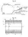
- Fig. 9 is a schematic diagram of the potential distribution in the dual-stage reflectron described in Patent Literature 1.
- the position P in Fig. 9 is a second-order focusing position in the conventional dual-stage reflectron in which correcting potential is not superimposed.
- correcting potential Zc(U) proportional to ⁇ U(Z)-E 0 ⁇ 3.5 is superimposed on potential Z A (U) of the uniform electric field. If the correcting potential Zc(U) is not superimposed, the time-of-flight spread is compensated for up to the second derivative of energy (the conventional technique of Mamyrin solution).
- an ion reflector forms an ion reflection electric field in its internal space with a plurality of guard-ring electrodes.
- Fig. 10 is a configuration diagram of a general ion reflector 4 including a plurality of guard-ring electrodes.
- a guard-ring electrode 401 is a substantially annular metal plate including an opening in the center. The shape of the opening is various, such as circular or rectangular, according to the path shapes of ions. Between adjacent guard-ring electrodes 401 of thickness Te, an insulating spacer 402 having thickness Ts is disposed. Thus, the interval between the adjacent two guard-ring electrodes 401 is Ts.
- the guard-ring electrode 401 and the spacer 402 having the same shapes are used in the first stage region S1 and the second stage region S2.
- the main reason is to reduce costs by using the guard-ring electrode 401 and the spacer 402 in common.
- Patent Literature 2 describes a method of disposing guard-ring electrodes at high position accuracy and inexpensively realizing the guard-ring electrodes.
- the thicknesses of a plurality of guard-ring electrodes are the same, and the interval between adjacent electrodes, that is, the thicknesses of spacers, are also the same.
- guard-ring electrodes it is desirable to dispose as many number of guard-ring electrodes at as narrow intervals as possible (i.e., at as high density as possible). It is also desirable to make the guard-ring electrodes as thin as possible. Further it is desirable to make the inner circumferential edge of the guard-ring electrodes as close as possible to the center axis.
- the above explanation about the disposition and the shape of the guard-ring electrodes is illustrated using an example of simulated calculation on potential distributions in the inner space of the guard-ring electrodes.
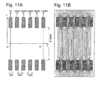
- the configuration and the shape of the guard-ring electrodes used for the calculation are shown in Fig. 11A .
- the guard-ring electrodes have a shape rotationally symmetrical with respect to the Z axis.
- the diameter of the opening through which ions pass is 100 [mm].
- Both the thickness Te of the guard-ring electrodes and the thickness Ts of the spacers are 10 [mm].
- applied voltages to the guard-ring electrodes are set to 0, 200, 400, 600, 800, and 1000 [V] respectively from the incident end electrode.
- Fig. 11B shows a calculation result of the potential distributions formed in the spaces in the guard-ring electrodes. Equipotential surfaces are shown at a 20 [V] interval.
- the guard-ring electrode should be as thin as possible to form the ideal potential distribution in the ion reflector.
- the grid electrodes G1 and G2 are provided respectively at the boundary between the non-electric field drift region and the first stage region S1 of the ion reflector, and at the boundary between the first stage region S1 and the second stage region S2 of the ion reflector in order to form electric fields having different strengths on the both sides of the boundaries and to allow ions to pass. If the grid electrode G1 or G2 has bent or slack, distortion in the potential distribution inside the ion reflector appears. Therefore, to achieve high performance, it is necessary to stretch the grid electrodes at high flatness.
- Non-Patent Literature 3 describes a method of stretching the grid electrodes without slack. If the grid electrodes are stretched on the inner circumferential wall surface facing the center opening of the guard-ring electrode, structurally speaking, the guard-ring electrode needs to be thicker than a certain value. Typically, to stretch the grid-electrodes without slack, the thickness of the guard-ring electrode needs to be approximately 5 to 10 [mm] or more.
- the thickness of a guard-ring electrode is as thin as approximately 2 [mm] or less.
- the guard-ring electrode and the spacer having the same shapes are respectively used in all regions in common.
- the thickness of the guard-ring electrode is set to 10 [mm] taking into account such circumstances.
- the guard-ring electrode is thick to this degree, unevenness of a potential distribution at a position, in particular, away from the center axis in the radial direction is conspicuous.
- the deviation between the actually obtained potential and the ideal potential increases and deterioration in isochronism for the ion packet increases.
- the guard-ring electrodes of the ion reflector such terms as “thick electrode” and “thin electrode” are used.
- the “thick electrode” indicates an electrode having thickness of approximately 5 to 10 mm or more.
- the “thin electrode” indicates an electrode having thickness of approximately 2 [mm] or less.
- the present invention has been devised to solve the problems and it is an object of the present invention to provide a TOFMS including an ion reflector that can bring a formed reflection electric field closer to an ideal state while suppressing costs.
- a time-of-flight mass spectrometer including: an ion ejector configured to impart a predetermined amount of energy to target ions; a non-electric field ion drift region configured to let the ions to fly freely; an ion reflector including a plurality of plate-like electrodes disposed along an ion path in order to reflect and return, with action of an electric field, the ions flown in the non-electric field ion drift region; a detector configured to detect the ions reflected by the ion reflector and returning through the non-electric field ion drift region, wherein a flight space of the ions by the ion reflector is sectioned into a first region where a deceleration electric field for decelerating the ions passed through the non-electric field ion drift region is formed and a second region where a reflection electric field for reflecting the ions decelerated in the first region is formed, and thickness of the plurality of electrodes disposed in the
- the reflection electric field formed in the second region only has to be an electric field for reflecting the ions decelerated by the deceleration electric field in the first region at a position corresponding to initial energy of the ions.
- the thicknesses of all the guard-ring electrodes constituting the ion reflector are the same.
- the thicknesses of the electrodes are made different between the first region having the action of only the deceleration for the ions and the second region having the action of reflecting the ions.
- the electrodes are thicker in the first region than in the second region.
- the electrodes (the guard-ring electrodes) constituting the ion reflector are increased in thickness as explained above, in particular, the curve of the equipotential surface at the position away from the center axis in the radial direction increases and deviation from the ideal potential increases.
- the deviation of the potential in the first region where only the deceleration of the ions is performed does not considerably affect time focusing of the ions, and does not substantially spoil isochronism.
- the deviation of the potential in the second region where the reflection for the ions is performed considerably affects the time focusing of the ions.
- the electrodes are thin in the second region, compared with the first region, the deviation from the ideal potential is suppressed even at the position away from the center axis in the radial direction. Consequently, it is possible to secure isochronism of the ion packet and attain high mass-resolving power.
- the non-electric field ion drift region and the first region of the ion reflector are partitioned by a grid-like electrode stretched to the opening of an electrode constituting the ion reflector, and the first region and the second region of the ion reflector are also partitioned by a grid-like electrode stretched to the opening of an electrode constituting the ion reflector. That is, the TOFMS is a gridded reflectron, rather than a grid-less reflectron.
- the non-electric field ion drift region and the first region of the ion reflector and the first region and the second region of the ion reflector are respectively partitioned by the grid-like electrodes (grid electrodes) to prevent, electric fields from interfering with each other, with the grid-like electrodes set as boundaries.
- the grid-like electrode that partitions the first region and the second region of the ion reflector is stretched to an electrode having thickness ((Te1/2)+(Te2/2)) of a half of the same thickness (Te1) of the plurality of electrodes disposed in the first region and the same thickness (Te2) of the plurality of electrodes disposed in the second region, and a stretching position of the grid-like electrode is a position of Tf2 from the inner side of the reflector.
- the grid-like electrodes only have to be stretched to, rather than the thin electrodes disposed in the second region, the electrodes that are thick compared with the electrodes. Therefore, it is possible to stretch the grid-like electrodes without bend and slack while using the thin electrode in the second region, and to avoid distortion of a potential distribution inside the ion reflector due to the electrodes.
- the influence on isochronism due to the thick electrode disposed in the first region is small.
- a member constituting the thick electrode disposed in the first region and a member constituting the thin electrode disposed in the second region may be a common member. That is, the thick electrode disposed in the first region is formed by stacking a plurality of the thin electrodes disposed in the second region.
- a general-purpose machining technique such as etching or punching, it is possible to inexpensively produce a large number of thin electrodes having the same shape from a thin large metal plate. Therefore, if the thick electrode is formed using the thin electrode, costs can be reduced compared with the thick electrode manufactured by machining.
- spacers are sandwiched between the electrodes adjacent to one another in the electrodes configuring the ion reflector, and the thickness of the electrodes and the disposition of the electrodes are adjusted so that all the spacers have the same thickness.
- This configuration enables all the spacers to be common, which reduces manufacturing costs of the ion reflector and facilitates adjustment during assembly.
- the electrodes can be disposed at high density because of the thin electrodes disposed in the second region. This minimizes the distortion of the equipotential surface due to the thickness of the electrodes to form the ideal correcting potential described in Patent Literature 1. Consequently, it is possible to realize a reflectron close to an ideal state as well as high mass-resolving power. Increasing the thickness of the electrodes disposed in the first region and widening the interval of the electrodes reduce the number of the electrodes disposed in the first region. Even in that case, the potential correction in the second region secures device performance such as the mass-resolving power, and a cost reduction is attained by reducing the number of the electrodes in a range not affecting performance.
- Fig. 14 is a diagram showing the electrode structure of the conventional ion reflector assumed in the simulation.
- the ion reflector assumed herein is a slit-shaped electrode that is a planar symmetrical structure in an X-axis direction and reflectional symmetry with respect to an X-Z plane. Therefore, in Fig. 14 , the electrode structure only in a plane in a +Y direction including the X-Z plane is drawn. This is the same in Fig. 2 to Fig. 4 and Fig. 7 referred to below.
- the ion reflector has the common structure in which both of a first stage region S1 and a second stage region S2 have guard-ring electrodes of the same thickness and spacers of the same thickness.
- the length of a non-electric field drift region is 1000 [mm]
- the length of the first stage region S1 is 100 [mm]
- the length of the second stage region S2 is 300 [mm].
- the guard-ring electrode is a so-called thick electrode to be easily stretched grid electrode.
- Slit-type opening width of the guard-ring electrodes is 40 [mm].
- Videal represents an ideal potential distribution obtained by superimposing correcting potential on potential of the uniform electric field and ⁇ V represents a distribution of potential deviation between ideal potential and actual potential.
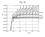
- Fig. 16 is a diagram showing a simulation result of a relative time-of-flight spread dT/T with respect to a relative energy spread dU/U in the case in which ions fly on the center axis and the paths deviating from the center axis in the ion reflector having the structure shown in Fig. 14 .
- Fig. 16 is a diagram showing a simulation result of a relative time-of-flight spread dT/T with respect to a relative energy spread dU/U in the case in which ions fly on the center axis and the paths deviating from the center axis in the ion reflector having the structure shown in Fig. 14 .
- ions having the relative energy spread dU/U of -0.2 correspond to ions reflected at a second-order focusing position (a correcting potential start point).
- Ions having -0.2 ⁇ dU/U ⁇ 0.2 correspond to ions reflected at a region where the correcting potential is superimposed on the potential of the uniform electric field. Isochronism is realized for these ion packets flying on the center axis.
- a cause of such deterioration of the mass-resolving power is the thickness of the guard-ring electrodes in the ion reflection region (in this example, the second stage region S2). Therefore, in the present invention, by forming the guard-ring electrodes thinner than those in the past in the ion reflection region, the mass-resolving power is improved for, in particular, the ions passing on the paths away from the center axis.
- Fig. 1 is a schematic configuration diagram of the TOFMS in this embodiment.
- Fig. 2 is a diagram showing the electrode structure of an ion reflector in the TOFMS in this embodiment.
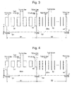
- Fig. 3 and Fig. 4 are diagrams respectively showing modifications of the electrode structure of the ion reflector.
- ions deriving from a sample generated by an ion source 1 are introduced into an ion-accelerating region 2.
- the ions are given initial energy by an electric field formed by a voltage applied to the ion-accelerating region 2 from an accelerating voltage source 7 in a pulse-like manner at predetermined timing and are sent to a flight space in a flight tube 3.
- An ion reflector 4 including a plurality of guard-ring electrodes 41, 42, and 43 and a terminal end electrode 44 disposed along an ion optical axis is set in the flight tube 3.
- a first grid electrode G1 is stretched to an opening of the guard-ring electrode 41 closest to the ion-accelerating region 2 among the electrodes.
- a second grid electrode G2 is stretched to an opening of another guard-ring electrode 43.
- Predetermined direct-current (DC) voltages are respectively applied to the guard-ring electrodes 41, 42, and 43 and the terminal end electrode 44 constituting the ion reflector 4 from a reflector DC voltage source 6 so that a static electric field (a direct-current electric field) having a predetermined potential shape is formed in an internal space of the ion reflector 4.
- the ions are reflected in the ion reflector 4 by the action of the electric field.
- the ions thus reflected and returned reach a detector 5.
- the detector 5 outputs a detection signal corresponding to a quantity of the reached ions.
- a controller 8 controls the accelerating voltage source 7, the reflector DC voltage source 6, and the like.
- a data processor 9 acquires timing information of acceleration of the ions, that is, information concerning flight start time from the controller 8, measures a flight time with reference to the timing information based on detection signals obtained from the respective ions, and converts the flight time into a mass-to-charge ratio m/z to create a mass spectrum.
- the ion source 1 can be an ion source using any ionization method such as MALDI, ESI, APCI, EI, or CI according to a form of a sample.
- the ion-accelerating region 2 only has to be a three-dimensional quadruple ion trap, a linear ion trap, or the like.
- the ion-accelerating region 2 may be a mere accelerating electrode that extracts and accelerates the ions generated by the ion source 1.
- the ion-accelerating region 2 can be configured from a pusher electrode and one or a plurality of grid electrodes.
- the guard-ring electrodes 41 including the beginning guard-ring electrode disposed between the first grid electrode G1 and the second grid electrode G2 have thickness Te1 of 8 [mm]
- the guard-ring electrodes 42 disposed between the second grid electrode G2 and the terminal end electrode 44 have thickness Te2 of 2 [mm]. That is, in this example, the thickness Te1 of the guard-ring electrodes 41 disposed in the first stage region S1 equivalent to the first region in the present invention is four times as large as the thickness Te2 of the guard-ring electrodes 42 disposed in the second stage region S2 equivalent to the second region in the present invention.
- the former is a so-called thick electrode and the latter is a so-called thin electrode.
- the second grid electrode G2 is attached to a position of 4 [mm] from an end on the first stage region S1 side of the guard-ring electrode 43.
- the thickness of a portion facing (included in) the first stage region S1 across the second grid electrode G2 is 4 [mm].
- the thickness of a portion facing (included in) the second stage region S2 is 1 [mm].
- the guard-ring electrodes 42 disposed in the second stage region S2 are considerably thin compared with the conventional general thickness of 5 to 10 [mm]. Therefore, a curve of an equipotential surface is small even in a position away from the center axis in the radial direction. Therefore, a spread of a time of flight decreases.
- spacers inserted among the guard-ring electrodes cannot be used in common due to the difference on the gaps (Ts1 and Ts2) between the adjacent guard-ring electrodes 41, 42 and 43in the first stage region S1 and the second stage region S2. This leads to an increase in costs.
- the pitch of the guard-ring electrodes and the thickness of the guard-ring electrodes are adjusted in each of the first stage region S1 and the second stage region S2 to modify the structure shown in Fig. 2 .
- Fig. 3 shows the modified structure.
- the electrode pitch of the guard-ring electrodes 41 disposed in the first stage region S1 is increased to 20 [mm].
- the spacers having the same size can be used for all the spacers, which results in cost reduction compared with the configuration shown in Fig. 2 requiring the two kinds of spacers having the different sizes.
- the number of the guard-ring electrodes 41 disposed in the first stage region S1 is also reduced from nine to four. Decreasing the number of electrodes requiring high accurate work contributes to cost reduction.
- slit width of the guard-ring electrodes 41 disposed in the first stage region S1 is increased to 60 [mm]. Otherwise, the structure is the same as that shown in Fig. 3 .
- simulation calculation was performed by the same method employed in the conventional ion reflector, and the result of the simulation calculation was compared with the result by the conventional ion reflector. In this case, in the deeper space (the right in Fig.
- Videal represents an ideal potential distribution obtained by superimposing correcting potential on potential of the uniform electric field and ⁇ V represents a distribution of potential deviation between ideal potential and actual potential.
- FIG. 6 is a diagram showing a simulation result of the relative time-of-flight spread dT/T with respect to the relative energy spread dU/U in the case in which ions fly on the center axis and the paths deviating from the center axis in the ion reflector according to the modification shown in Fig. 4 .
- a member constituting the thick electrode disposed in the first stage region S1 and a member constituting the thin electrode disposed in the second stage region S2 may be a common member.
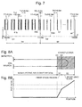
- Fig. 7 shows a modification of the electrode structure of the ion reflector where electrode arrangement is the same as that shown in Fig. 3 but the thick guard-ring electrode disposed in the first stage region S1 is formed with a stacked structure of a plurality of thin electrodes.
- a general-purpose machining technique such as etching or punching
- thin metal plate having the same shape and the same thickness is inexpensively produced in a large volume from a thin large metal plate.
- costs are reduced compared with when the thick electrode is manufactured by machining.
- the metal plate having thickness of 0.4 [mm] is used for both the electrodes 41b and 42.
- metal plate members having thickness Tf2 in the electrode 43b and the terminal end electrode 44 can be used in common.
- the ideal potential distribution is formed by introducing the non-uniform electric field into the second stage region S2 using the method described in Patent Literature 1.
- the sufficient advantage is also obtained in the TOFMS using the conventional ion reflector that forms only the uniform electric field by applying the present invention.
- the conventional dual-stage (or multistage) ion reflector that forms the uniform electric field it is also necessary to suppress unevenness of potential in the ion reflection region in order to improve mass-resolving power.
- the conventional ion reflector uses, as the ion flight space, the region near the center axis where the unevenness of the potential is sufficiently small.
- the region near the center axis where the unevenness of the potential is sufficiently small increases as the guard-ring electrodes are further reduced in thickness. Therefore, using the thin electrode as the guard-ring electrodes disposed in the region where the ions are reflected reduces the diameter of the ion reflector so as to advantageously allow the entire device to be compact.
- the opening shape of the guard-ring electrodes of the ion reflector has been assumed to be the round hole or the infinitely long slit shape.
- guard-ring electrodes having an opening shape of a rectangular shape or a long hole shape may be used.
- These opening shapes achieve satisfactory performance the same as those of the round hole or the infinitely long slit shape.
- the simulation is an example of the case where the present invention is applied to the dual-stage reflectron.
- the present invention also can be applied to an ion reflector including three or more stages.
- a final stage is an ion reflection region and the other stages are ion deceleration regions.
Landscapes
- Chemical & Material Sciences (AREA)
- Analytical Chemistry (AREA)
- Other Investigation Or Analysis Of Materials By Electrical Means (AREA)
Abstract
Description
- The present invention relates to a time-of-flight mass spectrometer (hereinafter referred to as "TOFMS") using an ion reflector, and more specifically to the structure of the ion reflector.
- In the TOFMS, the time of flight required for an ion packet (an aggregate of ions) ejected from an ion source supplied with a certain level of kinetic energy to reach a detector is measured, and the mass (or mass-to-charge ratio m/z, to be exact) of each ion is calculated from the time of flight. One major cause of deterioration in the mass-resolving power is spread in the initial energy of the ions. Spread in the initial energy of the ions ejected from the ion source causes broadening in the time-of-flight of the ions of the same mass, and deteriorates the mass-resolving power. To compensate for the time-of-flight broadening due to the initial energy spread of the ions, ion reflectors have been widely used. A TOFMS using the ion reflector is hereinafter called the "reflectron" according to the common practice.
- An ion reflector has an electric potential distribution in which the potential increases in the traveling direction of the ions, and has the function of reflecting ions coming through a drift space with free of electric field. An ion having a larger initial energy (initial speed) penetrates deeper into the ion reflector, and hence spends a longer time flying in the ion reflector when reflected. On the other hand, the ion having a larger initial energy flies at a higher speed and hence spends a shorter time flying through a non-electric field drift space. Therefore, by appropriately adjusting the parameters so as to cancel the increase in the time of flight in the ion reflector by the decrease in the time of flight in the non-electric field drift space, the total time of flight from the ion source to the detector becomes almost independent of the initial energy within a certain range of energy (see Non-Patent
Literature 1 for details). - Various types of reflectrons have been developed. A well-known reflectron is a dual-stage reflectron which was first developed by Mamyrin et al. (see Non-Patent Literature 2).
Fig. 8A is a schematic diagram showing an ion path in the dual-stage reflectron.Fig. 8B is a schematic diagram of a potential distribution on the center axis. - In the dual-stage reflectron, an ion reflector is constructed by two stages of uniform electric fields (a uniform electric field is an electric field in which the potential changes proportional to the distance), i.e., a first stage region S1 and a second stage region S2. Grid electrodes G1 and G2 including a large number of openings through which ions can pass are respectively set in the boundary between a non-electric field drift region and the first stage uniform electric field (the first stage region S1) and the boundary between the first stage uniform electric field and the second stage uniform electric field (the second stage region S2). That is, the non-electric field drift region and the first stage region S1 are partitioned by the grid electrode G1. The first stage region S1 and the second stage region S2 are partitioned by the grid electrode G2. Usually, the first stage region S1 is shorter than the second stage region S2, and, provided that approximately two thirds of the initial energy of ions is lost in the first stage region S1, the total time-of-flight spread is compensated to the second derivative of the energy (that is, the second-order energy focusing is achieved). Therefore, the time-of-flight broadening for an ion packet having initial energy spread to some extent can be small. As a result, high mass-resolving power is obtained. Such a dual-stage reflectron is most widely used in commercially available time-of-flight mass spectrometers.
- As explained above, in the dual-stage reflectron, basically, the electric fields are uniform electric fields in the stages of the ion reflector. It is known that energy-focusing performance can be improved by appropriately correcting the potential distribution of a part of the electric field to be a non-uniform electric field. For example, in
Patent Literature 1, the present inventors propose a new TOFMS that realizes isochronism for an ion packet having energy equal to or larger than a certain energy threshold and flying on the center axis, by slightly correcting the potential distribution of the second stage region S2 in the dual-stage reflectron. -
Fig. 9 is a schematic diagram of the potential distribution in the dual-stage reflectron described inPatent Literature 1. The position P inFig. 9 is a second-order focusing position in the conventional dual-stage reflectron in which correcting potential is not superimposed. In a deeper space starting from the second-order focusing position P, correcting potential Zc(U) proportional to {U(Z)-E0}3.5 is superimposed on potential ZA(U) of the uniform electric field. If the correcting potential Zc(U) is not superimposed, the time-of-flight spread is compensated for up to the second derivative of energy (the conventional technique of Mamyrin solution). However, the time-of-flight spread is compensated for up to the third and infinitely continuing higher-order derivatives that cannot be compensated by the Mamyrin solution, by superimposing correcting potential Zc(U). Consequently, complete isochronism can be realized for ions reflected in the correcting potential portion. Potential distribution curves are smoothly connected before and behind the second-order focusing position P. Further, the correcting potential Zc(U) is extremely small compared with the potential ZA(U) of the uniform electric field. Therefore, not only theoretically, it is relatively easy to actually superimpose such correcting potential Zc(U). In the explanation, Z represents a coordinate along the center axis of the ion reflector, U represents a potential value in the coordinate Z, and Eo represents a potential value in the second-order focusing position P. - According to the method explained above, it is possible in principle, to realize an ideal reflectron. In actual, it is necessary to form a theoretically calculated ideal correcting potential distribution on the center axis inside the ion reflector. However, it is difficult in a conventional general ion reflector to form this highly accurate potential distribution. A reason for this is explained below.
- In general, an ion reflector forms an ion reflection electric field in its internal space with a plurality of guard-ring electrodes.
Fig. 10 is a configuration diagram of ageneral ion reflector 4 including a plurality of guard-ring electrodes. A guard-ring electrode 401 is a substantially annular metal plate including an opening in the center. The shape of the opening is various, such as circular or rectangular, according to the path shapes of ions. Between adjacent guard-ring electrodes 401 of thickness Te, an insulatingspacer 402 having thickness Ts is disposed. Thus, the interval between the adjacent two guard-ring electrodes 401 is Ts. As shown in the drawing, in the conventional general dual-stage reflectron, the guard-ring electrode 401 and thespacer 402 having the same shapes are used in the first stage region S1 and the second stage region S2. The main reason is to reduce costs by using the guard-ring electrode 401 and thespacer 402 in common. - The mass-resolving power of the general TOFMS currently on the market is 10000 or more. To realize the high mass-resolving power to this extent, it is necessary to dispose the guard-
ring electrode 401 at high position accuracy in micron order. Therefore, it is necessary to manufacture the guard-ring electrode 401 and thespacer 402 at high accuracy, and further assemble them at high accuracy.Patent Literature 2 describes a method of disposing guard-ring electrodes at high position accuracy and inexpensively realizing the guard-ring electrodes. In the literature, the thicknesses of a plurality of guard-ring electrodes are the same, and the interval between adjacent electrodes, that is, the thicknesses of spacers, are also the same. - To form the non-uniform ideal potential distribution as described above along the center axis inside the ion reflector, it is desirable to dispose as many number of guard-ring electrodes at as narrow intervals as possible (i.e., at as high density as possible). It is also desirable to make the guard-ring electrodes as thin as possible. Further it is desirable to make the inner circumferential edge of the guard-ring electrodes as close as possible to the center axis.
- The above explanation about the disposition and the shape of the guard-ring electrodes is illustrated using an example of simulated calculation on potential distributions in the inner space of the guard-ring electrodes. The configuration and the shape of the guard-ring electrodes used for the calculation are shown in
Fig. 11A . The guard-ring electrodes have a shape rotationally symmetrical with respect to the Z axis. The diameter of the opening through which ions pass is 100 [mm]. Both the thickness Te of the guard-ring electrodes and the thickness Ts of the spacers (the interval between the adjacent electrodes) are 10 [mm]. The grid electrode G is placed at a position half the thickness of a guard-ring electrode, that is, the position of Tf=Te/2=5 [mm] thickness. To form a uniform electric field along the Z axis in the guard-ring electrodes having such a shape, applied voltages to the guard-ring electrodes are set to 0, 200, 400, 600, 800, and 1000 [V] respectively from the incident end electrode. -
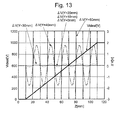
Fig. 11B shows a calculation result of the potential distributions formed in the spaces in the guard-ring electrodes. Equipotential surfaces are shown at a 20 [V] interval.Fig. 12 is potential distributions on the Z axis (Y=0) and the line parallel to the Z axis at Y=50 [mm].Fig. 13 is an ideal potential distribution of the uniform electric field (Videal) and a distribution of deviation (ΔV=V-Videal) between the ideal potential of the uniform electric field and potential actually formed on the Z axis and lines parallel to the Z axis at Y=10, 20, 30, 40, and 50 [mm]. - The following is found from the results shown in
Fig. 11 to Fig. 13 . - (1) According to
Fig. 12 andFig. 13 , although the actual potential distribution is close to the ideal potential of the uniform electric field near the center axis (Y=0) of the ion reflector, the deviation between the ideal potential and the actual potential increases at a position further away from the center axis and closer the guard-ring electrode 401 (i.e., Y is larger). - (2) As shown in
Fig. 11B , a curve of an equipotential surface is larger at a position closer to the guard-ring electrode 401. Since it is certain that, if the guard-ring electrode 401 is thinner, the curvature will be smaller (curve will be milder), it is apparent that the deviation of the potential explained in (1) is caused by the thickness of the guard-ring electrode 401. In other words, it is considered that, as the guard-ring electrode 401 is thinner, deviation of the potential at a position away from the center axis by distance Y is smaller (the deviation is zero if the guard-ring electrode is infinitely thin). - As explained above, the guard-ring electrode should be as thin as possible to form the ideal potential distribution in the ion reflector. However, actually, there are limitations. As shown in
Fig. 8B andFig. 9 , the grid electrodes G1 and G2 are provided respectively at the boundary between the non-electric field drift region and the first stage region S1 of the ion reflector, and at the boundary between the first stage region S1 and the second stage region S2 of the ion reflector in order to form electric fields having different strengths on the both sides of the boundaries and to allow ions to pass. If the grid electrode G1 or G2 has bent or slack, distortion in the potential distribution inside the ion reflector appears. Therefore, to achieve high performance, it is necessary to stretch the grid electrodes at high flatness. For example,Non-Patent Literature 3 describes a method of stretching the grid electrodes without slack. If the grid electrodes are stretched on the inner circumferential wall surface facing the center opening of the guard-ring electrode, structurally speaking, the guard-ring electrode needs to be thicker than a certain value. Typically, to stretch the grid-electrodes without slack, the thickness of the guard-ring electrode needs to be approximately 5 to 10 [mm] or more. - In a so-called gird-less reflector, commercialized by some manufacturers, which does not use a grid at the boundary before and behind a first stage region, in some case, the thickness of a guard-ring electrode is as thin as approximately 2 [mm] or less. However, it is practically impossible to stretch a grid electrode at such thickness of a guard-ring electrode. In such a grid-less reflector, as in the ion reflector using grids, the guard-ring electrode and the spacer having the same shapes are respectively used in all regions in common.
- In the simulation, the thickness of the guard-ring electrode is set to 10 [mm] taking into account such circumstances. However, as it is evident from the above result, when the guard-ring electrode is thick to this degree, unevenness of a potential distribution at a position, in particular, away from the center axis in the radial direction is conspicuous. As a result, even if it is attempted, for example, to superimpose the correcting potential on the potential of the uniform electric field to form the ideal potential distribution, the deviation between the actually obtained potential and the ideal potential increases and deterioration in isochronism for the ion packet increases.
- In the following explanation, with respect to the guard-ring electrodes of the ion reflector, such terms as "thick electrode" and "thin electrode" are used. In relation to the conventional technique explained above, the "thick electrode" indicates an electrode having thickness of approximately 5 to 10 mm or more. On the other hand, the "thin electrode" indicates an electrode having thickness of approximately 2 [mm] or less.
-
- [Patent Literature 1]
WO2012/086630 - [Patent Literature 2]
US6,849,846 A -
- [Non Patent Literature 1] R. J Cotter, "Time-of-Flight Mass Spectrometry: Instrumentation and Applications in Biological Research" American Chemical Society, 1997
- [Non Patent Literature 2]B.A. Mamyrin and three others," The mass-reflectron, a new nonmagnetic time-of-flight mass spectrometer with high resolution", Sov. Phys. -JETP 37, 1973, p.45-48
- [Non Patent Literature 3]T. Bergmann and two others, "High resolution time-of-flight mass spectrometers. Part III. Reflector design", Review of Scientific Instruments, 61(10), 1990, p.2592-2600
- The present invention has been devised to solve the problems and it is an object of the present invention to provide a TOFMS including an ion reflector that can bring a formed reflection electric field closer to an ideal state while suppressing costs.
- The present invention devised to solve the problems is a time-of-flight mass spectrometer including: an ion ejector configured to impart a predetermined amount of energy to target ions; a non-electric field ion drift region configured to let the ions to fly freely; an ion reflector including a plurality of plate-like electrodes disposed along an ion path in order to reflect and return, with action of an electric field, the ions flown in the non-electric field ion drift region; a detector configured to detect the ions reflected by the ion reflector and returning through the non-electric field ion drift region, wherein
a flight space of the ions by the ion reflector is sectioned into a first region where a deceleration electric field for decelerating the ions passed through the non-electric field ion drift region is formed and a second region where a reflection electric field for reflecting the ions decelerated in the first region is formed, and
thickness of the plurality of electrodes disposed in the second region is set small compared with thickness of the plurality of electrodes disposed in the first region. - In the present invention, the reflection electric field formed in the second region only has to be an electric field for reflecting the ions decelerated by the deceleration electric field in the first region at a position corresponding to initial energy of the ions.
- As explained above, in the conventional general reflectron, the thicknesses of all the guard-ring electrodes constituting the ion reflector are the same. On the other hand, in the TOFMS according to the present invention, the thicknesses of the electrodes are made different between the first region having the action of only the deceleration for the ions and the second region having the action of reflecting the ions. The electrodes are thicker in the first region than in the second region. As a specific mode, it is desirable to set the thickness of each of the plurality of electrodes disposed in the second region to approximately 2 mm or less, and set the thickness of each of the plurality of electrodes disposed in the first region to 5 to 10 mm or more.
- When the electrodes (the guard-ring electrodes) constituting the ion reflector are increased in thickness as explained above, in particular, the curve of the equipotential surface at the position away from the center axis in the radial direction increases and deviation from the ideal potential increases. However, according to a study using the simulated calculation by the present inventors, the deviation of the potential in the first region where only the deceleration of the ions is performed does not considerably affect time focusing of the ions, and does not substantially spoil isochronism. On the other hand, the deviation of the potential in the second region where the reflection for the ions is performed considerably affects the time focusing of the ions. In the TOFMS according to the present invention, since the electrodes (the guard-ring electrodes) are thin in the second region, compared with the first region, the deviation from the ideal potential is suppressed even at the position away from the center axis in the radial direction. Consequently, it is possible to secure isochronism of the ion packet and attain high mass-resolving power.
- As a typical mode of the time-of-flight mass spectrometer according to the present invention, the non-electric field ion drift region and the first region of the ion reflector are partitioned by a grid-like electrode stretched to the opening of an electrode constituting the ion reflector, and the first region and the second region of the ion reflector are also partitioned by a grid-like electrode stretched to the opening of an electrode constituting the ion reflector. That is, the TOFMS is a gridded reflectron, rather than a grid-less reflectron. The non-electric field ion drift region and the first region of the ion reflector and the first region and the second region of the ion reflector are respectively partitioned by the grid-like electrodes (grid electrodes) to prevent, electric fields from interfering with each other, with the grid-like electrodes set as boundaries.
- In the time-of-flight mass spectrometer having the mode explained above, it is desirable that the grid-like electrode that partitions the non-electric field ion drift region and the first region of the ion reflector is stretched to an electrode having thickness equal to or larger than a half (Tf1=Te1/2) of the same thickness (Te1) of the plurality of electrodes disposed in the first region, and a stretching position of the grid-like electrode is a position of Tf1 from an inner side of the reflector. It is desirable that the grid-like electrode that partitions the first region and the second region of the ion reflector is stretched to an electrode having thickness ((Te1/2)+(Te2/2)) of a half of the same thickness (Te1) of the plurality of electrodes disposed in the first region and the same thickness (Te2) of the plurality of electrodes disposed in the second region, and a stretching position of the grid-like electrode is a position of Tf2 from the inner side of the reflector.
- With this configuration, the grid-like electrodes only have to be stretched to, rather than the thin electrodes disposed in the second region, the electrodes that are thick compared with the electrodes. Therefore, it is possible to stretch the grid-like electrodes without bend and slack while using the thin electrode in the second region, and to avoid distortion of a potential distribution inside the ion reflector due to the electrodes.
- As explained above, the influence on isochronism due to the thick electrode disposed in the first region is small. In order to further improve the mass-resolving power, it is desirable to form an opening of the thick electrode disposed in the first region larger than an opening of the thin electrode disposed in the second region.
- As the curve of the equipotential surface due to the thick electrode is large in the vicinity of the electrode inner circumferential edge portion facing the opening, widening the opening softens the curve degree of the equipotential surface at the position having the same distance from the center axis. Consequently, the deviation between the actual potential and the ideal potential at the position having the same distance from the center axis decreases. The broadening of the time-of-flight which occurs in the ions passing a path deviating from the center axis in the first region decreases. This leads to improvement of comprehensive isochronism.
- In order to further reduce manufacturing costs of the ion reflector, a member constituting the thick electrode disposed in the first region and a member constituting the thin electrode disposed in the second region may be a common member. That is, the thick electrode disposed in the first region is formed by stacking a plurality of the thin electrodes disposed in the second region. By using a general-purpose machining technique such as etching or punching, it is possible to inexpensively produce a large number of thin electrodes having the same shape from a thin large metal plate. Therefore, if the thick electrode is formed using the thin electrode, costs can be reduced compared with the thick electrode manufactured by machining.
- In the time-of-flight mass spectrometer according to the present invention, preferably, spacers are sandwiched between the electrodes adjacent to one another in the electrodes configuring the ion reflector, and the thickness of the electrodes and the disposition of the electrodes are adjusted so that all the spacers have the same thickness. This configuration enables all the spacers to be common, which reduces manufacturing costs of the ion reflector and facilitates adjustment during assembly.
- With the time-of-flight mass spectrometer according to the present invention, the electrodes can be disposed at high density because of the thin electrodes disposed in the second region. This minimizes the distortion of the equipotential surface due to the thickness of the electrodes to form the ideal correcting potential described in
Patent Literature 1. Consequently, it is possible to realize a reflectron close to an ideal state as well as high mass-resolving power. Increasing the thickness of the electrodes disposed in the first region and widening the interval of the electrodes reduce the number of the electrodes disposed in the first region. Even in that case, the potential correction in the second region secures device performance such as the mass-resolving power, and a cost reduction is attained by reducing the number of the electrodes in a range not affecting performance. -
-
Fig. 1 is a schematic configuration diagram of a TOFMS according to an embodiment of the present invention. -
Fig. 2 is a diagram showing the electrode structure of an ion reflector in the TOFMS in the embodiment. -
Fig. 3 is a diagram showing a modification of the electrode structure of the ion reflector in the TOFMS in the embodiment. -
Fig. 4 is a diagram showing a modification of the electrode structure of the ion reflector in the TOFMS in the embodiment. -
Fig. 5 is a diagram showing a simulation result of a potential distribution on a center axis and on paths deviating from the center axis in the ion reflector having the structure shown inFig. 4 . -
Fig. 6 is a diagram showing a simulation result of a relative time spread dT/T with respect to a relative energy spread dU/U in the case in which ions fly on the center axis and on the paths deviating from the center axis in the ion reflector having the structure shown inFig. 4 . -
Fig. 7 is a diagram showing another modification of the electrode structure of the ion reflector in the TOFMS in the embodiment. -
Fig. 8A is a schematic diagram showing an ion path in a dual-stage reflectron of the conventional technique andFig. 8B is a schematic diagram of a potential distribution on the center axis. -
Fig. 9 is a conceptual diagram of a potential distribution of a dual-stage reflectron described inPatent Literature 1. -
Fig. 10 is a configuration diagram of a general ion reflector. -
Fig. 11A is a diagram showing the configuration and the shape of guard-ring electrodes used for a simulation andFig. 11B is a diagram showing a simulation result of potential distributions formed in spaces in the guard-ring electrodes. -
Fig. 12 is a diagram showing potential distributions on a Z axis (Y=0) ant on a line parallel to the Z axis at Y=50 [mm]. -
Fig. 13 is a diagram showing an ideal potential distribution by a uniform electric field and a distribution of deviation between the ideal potential distribution by the uniform electric field and potentials actually formed on the Z axis and lines parallel to the Z axis at Y=10, 20, 30, 40, and 50 [mm]. -
Fig. 14 is a diagram showing the structure of guard-ring electrodes of a conventional ion reflector used for a simulation for comparing with the ion reflector according to the present invention. -
Fig. 15 is a diagram showing a simulation result of potential distributions on a center axis and on paths deviating from the center axis in the ion reflector having the structure shown inFig. 14 . -
Fig. 16 is a diagram showing a simulation result of a relative time-of-flight spread dT/T with respect to a relative energy spread dU/U in the case in which ions fly on the center axis and the tracks deviating from the center axis in the ion reflector having the structure shown inFig. 14 . - Before explaining an embodiment of the present invention, a detailed simulation result of deviation of potential and a relation between a relative energy spread and a relative time-of-flight spread due to the deviation in the electrode structure of the conventional ion reflector is explained.
Fig. 14 is a diagram showing the electrode structure of the conventional ion reflector assumed in the simulation. The ion reflector assumed herein is a slit-shaped electrode that is a planar symmetrical structure in an X-axis direction and reflectional symmetry with respect to an X-Z plane. Therefore, inFig. 14 , the electrode structure only in a plane in a +Y direction including the X-Z plane is drawn. This is the same inFig. 2 to Fig. 4 andFig. 7 referred to below. - As shown in
Fig. 14 , the ion reflector has the common structure in which both of a first stage region S1 and a second stage region S2 have guard-ring electrodes of the same thickness and spacers of the same thickness. The length of a non-electric field drift region is 1000 [mm], the length of the first stage region S1 is 100 [mm], and the length of the second stage region S2 is 300 [mm]. The thickness of one guard-ring electrode is Te1=Te2=5 [mm]. The guard-ring electrode is a so-called thick electrode to be easily stretched grid electrode. The thickness of the spacers is Ts1= Ts2=5 [mm]. A first grid electrode G1 is attached at a position of a half in the thickness direction of a beginning guard-ring electrode, that is a position of thickness Tf1=2.5 [mm]. A second grid electrode G2 is attached at a position of a half in the thickness direction of a predetermined guard-ring electrode, that is, a position of thickness Tf1=Tf2=2.5 [mm]. Slit-type opening width of the guard-ring electrodes is 40 [mm]. - Voltages were respectively applied to the guard-ring electrodes of the ion reflector set as explained above and adjusted for obtaining an ideal potential distribution on a center path (the Z axis in
Fig. 14 ). A time of flight of ions was examined with a simulation by changing initial energy of the ions. The method described inPatent Literature 1 was used to obtain the ideal potential distribution. That is, in a deeper side (the right side inFig. 14 ) starting from a second-order focusing position set in the second stage region S2, correcting potential Zc(U) proportional to {U(Z)-E0}3.5 is superimposed on potential ZA(U) of the uniform electric field to cancel even a third-order or higher temporal aberration. -
Fig. 15 is a diagram showing a simulation result of potential distributions on a center axis (Y=0 [mm]) and paths (Y=2.5, 5, and 7.5 [mm]) deviating from the center axis in the ion reflector having the structure shown inFig. 14 . In the figure, Videal represents an ideal potential distribution obtained by superimposing correcting potential on potential of the uniform electric field and ΔV represents a distribution of potential deviation between ideal potential and actual potential. -
Fig. 16 is a diagram showing a simulation result of a relative time-of-flight spread dT/T with respect to a relative energy spread dU/U in the case in which ions fly on the center axis and the paths deviating from the center axis in the ion reflector having the structure shown inFig. 14 . The ordinate dT/T ofFig. 16 represents a time of flight as a relative value with reference to a time of flight at the time when the relative energy spread dU/U of the ions is 0 and Y=0 (i.e., on the center axis). InFig. 16 , ions having the relative energy spread dU/U of -0.2 correspond to ions reflected at a second-order focusing position (a correcting potential start point). Ions having -0.2<dU/U<0.2 correspond to ions reflected at a region where the correcting potential is superimposed on the potential of the uniform electric field. Isochronism is realized for these ion packets flying on the center axis. - Looking at the potential distribution inside the ion reflector shown in
Fig. 15 , since the correcting potential is superimposed as explained above, it is seen that Y-coordinate dependency of a potential distribution is more conspicuous on the region deeper than the vicinity of a correction start point near Z=1180. The potential deviation ΔV is substantially zero and ideal potential can be substantially realized on the center axis (Y=0 [mm]). On the other hand, further away from the center axis, the potential deviationΔV increases and unevenness is clearly observed in the deviation of the potential. The unevenness coincides with a pitch of the guard-ring electrodes, which means that the unevenness of the deviation of the potential is due to the thickness of the guard-ring electrodes. - Looking at initial energy dependency of the time of flight shown in
Fig. 16 , it is seen that variation of the time of flight due to the unevenness of the potential clearly increases with an increase in a Y coordinate (further away from the center axis). Since the mass-resolving power is given by R=(1/2)(T/dT), a time difference dT/T=1E-5 corresponds to mass-resolving power 50000 and a time difference dT/T=2E-5 corresponds to resolving power 25000. From these results, it is seen that, in the structure of the conventional ion reflector, although high mass-resolving power is obtained as long as a flight space of the ions is limited to a narrow region around the center axis, the position away from the center axis 5 [mm] or more incurs the unevenness of the potential formed by the guard-ring electrodes in the second stage region S2 and thus the time of flight spread, which results in deterioration in the mass-resolving power. - As explained above, a cause of such deterioration of the mass-resolving power is the thickness of the guard-ring electrodes in the ion reflection region (in this example, the second stage region S2). Therefore, in the present invention, by forming the guard-ring electrodes thinner than those in the past in the ion reflection region, the mass-resolving power is improved for, in particular, the ions passing on the paths away from the center axis.
- A TOFMS in the embodiment of the present invention is explained below with reference to the accompanying drawings.
Fig. 1 is a schematic configuration diagram of the TOFMS in this embodiment.Fig. 2 is a diagram showing the electrode structure of an ion reflector in the TOFMS in this embodiment.Fig. 3 and Fig. 4 are diagrams respectively showing modifications of the electrode structure of the ion reflector. - In
Fig. 1 , ions deriving from a sample generated by anion source 1 are introduced into an ion-acceleratingregion 2. The ions are given initial energy by an electric field formed by a voltage applied to the ion-acceleratingregion 2 from an acceleratingvoltage source 7 in a pulse-like manner at predetermined timing and are sent to a flight space in aflight tube 3. Anion reflector 4 including a plurality of guard-ring electrodes terminal end electrode 44 disposed along an ion optical axis is set in theflight tube 3. A first grid electrode G1 is stretched to an opening of the guard-ring electrode 41 closest to the ion-acceleratingregion 2 among the electrodes. A second grid electrode G2 is stretched to an opening of another guard-ring electrode 43. - Predetermined direct-current (DC) voltages are respectively applied to the guard-
ring electrodes terminal end electrode 44 constituting theion reflector 4 from a reflectorDC voltage source 6 so that a static electric field (a direct-current electric field) having a predetermined potential shape is formed in an internal space of theion reflector 4. The ions are reflected in theion reflector 4 by the action of the electric field. The ions thus reflected and returned reach adetector 5. Thedetector 5 outputs a detection signal corresponding to a quantity of the reached ions. Acontroller 8 controls the acceleratingvoltage source 7, the reflectorDC voltage source 6, and the like. A data processor 9 acquires timing information of acceleration of the ions, that is, information concerning flight start time from thecontroller 8, measures a flight time with reference to the timing information based on detection signals obtained from the respective ions, and converts the flight time into a mass-to-charge ratio m/z to create a mass spectrum. - The
ion source 1 can be an ion source using any ionization method such as MALDI, ESI, APCI, EI, or CI according to a form of a sample. The ion-acceleratingregion 2 only has to be a three-dimensional quadruple ion trap, a linear ion trap, or the like. When theion source 1 is the ion source of MALDI or the like, the ion-acceleratingregion 2 may be a mere accelerating electrode that extracts and accelerates the ions generated by theion source 1. To suppress variation of the initial energy of the ions, it is desirable to adopt an orthogonal acceleration method of accelerating the ions extracted from theion source 1 in a direction orthogonal to the extracting direction from the ion source and sends the ions into theflight tube 3. In that case, the ion-acceleratingregion 2 can be configured from a pusher electrode and one or a plurality of grid electrodes. - As shown in
Fig. 2 , the guard-ring electrodes 41 including the beginning guard-ring electrode disposed between the first grid electrode G1 and the second grid electrode G2 (that is, in the first stage region S1) have thickness Te1 of 8 [mm], while the guard-ring electrodes 42 disposed between the second grid electrode G2 and the terminal end electrode 44 (that is, in the second stage region S2) have thickness Te2 of 2 [mm]. That is, in this example, the thickness Te1 of the guard-ring electrodes 41 disposed in the first stage region S1 equivalent to the first region in the present invention is four times as large as the thickness Te2 of the guard-ring electrodes 42 disposed in the second stage region S2 equivalent to the second region in the present invention. The former is a so-called thick electrode and the latter is a so-called thin electrode. In both of the first stage region S1 and the second stage region S2, a pitch of the guard-ring electrodes ring electrodes 41 adjacent to each other is Ts1=2 [mm]. In the second stage region S2, a gap between the guard-ring electrodes 42 adjacent to each other is Ts2=8 [mm]. Slit-type opening width of the guard-ring electrodes - The first grid electrode G1 is attached to the top guard-
ring electrode 41 in a position of a half in the thickness direction of the guard-ring electrodes 41 disposed in the first stage S1, that is, a position of thickness Tf1=Te1/2=4 [mm] from the inner side of the reflector. Therefore, in the beginning guard ring electrode, the thickness of a portion facing (included in) the first stage region S1 across the first grid electrode G1 is 4 [mm]. On the other hand, the thickness of the guard-ring electrode 43, to which the second grid electrode G2 is attached, is 5 [mm] obtained by adding up a half of the thickness Te1=8 [mm] of the guard-ring electrodes 41 disposed in the first stage region S1 and a half of the thickness Te2=2 [mm] of the guard-ring electrodes 42 disposed in the second stage region S2. The second grid electrode G2 is attached to a position of 4 [mm] from an end on the first stage region S1 side of the guard-ring electrode 43. The thickness of a portion facing (included in) the first stage region S1 across the second grid electrode G2 is 4 [mm]. The thickness of a portion facing (included in) the second stage region S2 is 1 [mm]. By setting the substantial thicknesses of the electrodes at the ends (start end and terminal end) of the stages to the halves of the thicknesses of the electrodes included in the stages, it is possible to form an ideal uniform electric field even near the grid electrodes. - As shown in
Fig. 2 , the guard-ring electrodes 42 disposed in the second stage region S2 are considerably thin compared with the conventional general thickness of 5 to 10 [mm]. Therefore, a curve of an equipotential surface is small even in a position away from the center axis in the radial direction. Therefore, a spread of a time of flight decreases. In this configuration, unlike the conventional configuration shown inFig. 10 , spacers inserted among the guard-ring electrodes cannot be used in common due to the difference on the gaps (Ts1 and Ts2) between the adjacent guard-ring electrodes Fig. 2 .Fig. 3 shows the modified structure. - That is, in the modified structure shown in
Fig. 3 , the thickness of the guard-ring electrodes 42 disposed in the second stage region S2 is further reduced to Te2=0.4 [mm]. The interval between the adjacent electrodes, that is, the thickness of the spacers is adjusted to Ts1=Ts2=9.6 [mm] common to the first stage region S1 and the second stage region S2. Accordingly, the electrode pitch of the guard-ring electrodes 41 disposed in the first stage region S1 is increased to 20 [mm]. The thickness of theelectrodes 41 is further increased to Te1=10.4 [mm]. In such a configuration, the spacers having the same size can be used for all the spacers, which results in cost reduction compared with the configuration shown inFig. 2 requiring the two kinds of spacers having the different sizes. The number of the guard-ring electrodes 41 disposed in the first stage region S1 is also reduced from nine to four. Decreasing the number of electrodes requiring high accurate work contributes to cost reduction. - On the other hand, unevenness of the potential on the center axis in the first stage region S1 increases because of an increase in thickness of the guard-
ring electrodes 41 disposed in the first stage region S1. As explained below, actually, although the unevenness of the potential in the first stage region S1 hardly affects overall isochronism, when realization of higher isochronism is taken into account, it is desirable to suppress the unevenness of the potential in the first stage region S1 as much as possible. To address this, the center opening of the guard-ring electrodes 41 disposed in the first stage region S1 is widened to further modify the structure shown inFig. 3. Fig. 4 shows the modified structure. - As shown in
Fig. 4 , in the structure of the modification, slit width of the guard-ring electrodes 41 disposed in the first stage region S1 is increased to 60 [mm]. Otherwise, the structure is the same as that shown inFig. 3 . Based on the electrode structure of the ion reflector shown inFig. 4 , which is more advantageous than the structure shown inFig. 2 in terms of costs and has performance equivalent to or higher than the structure shown inFig. 3 , simulation calculation was performed by the same method employed in the conventional ion reflector, and the result of the simulation calculation was compared with the result by the conventional ion reflector. In this case, in the deeper space (the right inFig. 4 ) starting from a second-order focusing position set in the second stage region S2, correcting potential Zc(U) proportional to {U(Z)-E0}3.5 is superimposed on potential ZA(U) of the uniform electric field using the method described inPatent Literature 1 to form an ideal potential distribution on the center axis. -
Fig. 5 is a diagram showing a simulation result of potential distributions on a center axis (Y=0 [mm]) and paths (Y=2.5, 5, and 7.5 [mm]) deviating from the center axis in the ion reflector according to the modification shown inFig. 4 . As inFig. 15 , Videal represents an ideal potential distribution obtained by superimposing correcting potential on potential of the uniform electric field and ΔV represents a distribution of potential deviation between ideal potential and actual potential.Fig. 6 is a diagram showing a simulation result of the relative time-of-flight spread dT/T with respect to the relative energy spread dU/U in the case in which ions fly on the center axis and the paths deviating from the center axis in the ion reflector according to the modification shown inFig. 4 . - As is evident from the comparison with
Fig. 5 andFig. 15 , in the structure shown inFig. 4 , since the guard-ring electrodes 42 disposed in the second stage region S2 are reduced in thickness, it is seen that the unevenness of the potential conspicuous at, in particular, Y=5 and 7.5 [mm] away from the center axis is substantially reduced. Since the unevenness of the potential is greatly improved in this way, as shown inFig. 6 , it is seen that the spread of the time of flight is greatly improved even on the tracks away from the center axis. That means, with the TOFMS in this embodiment, not only an ion packet flying on the center axis but also an ion packet flying on the paths away from the center axis realize isochronism at a high level and attain high mass-resolving power. With the structure shown inFig. 3 and Fig. 4 , there is not only an advantage to reduce unevenness of the potential in the ion reflection region that greatly affects the mass-resolving power but also an advantage to reduce the number of the guard-ring electrodes 41 disposed in the first stage region S1 compared with the conventional structure. The reduction above is combined with usage of the common spacers so that further effective in cost reduction is achieved. - In order to further reduce the manufacturing costs of the ion reflector, a member constituting the thick electrode disposed in the first stage region S1 and a member constituting the thin electrode disposed in the second stage region S2 may be a common member.
Fig. 7 shows a modification of the electrode structure of the ion reflector where electrode arrangement is the same as that shown inFig. 3 but the thick guard-ring electrode disposed in the first stage region S1 is formed with a stacked structure of a plurality of thin electrodes. In this example, a guard-ring electrode 41b having thickness Te1=10.4 [mm] disposed in the first stage region S1 is formed by stacking twenty-six guard-ring electrodes 42 having thickness Te2=0.4 [mm] disposed in the second stage region S2. A guard-ring electrode 43b, to which the second grid electrode G2 is attached, is formed by stacking thirteen guard-ring electrodes 42 having thickness Te2=0.4 [mm] and further stacking one metal plate having thickness of 0.2 [mm] on the guard-ring electrodes 42. By using a general-purpose machining technique such as etching or punching, thin metal plate having the same shape and the same thickness is inexpensively produced in a large volume from a thin large metal plate. By forming the thick electrode using the metal plate member used in the thin electrode in this way, costs are reduced compared with when the thick electrode is manufactured by machining. - In the example shown in
Fig. 7 , the metal plate having thickness of 0.4 [mm] is used for both theelectrodes electrode 43b and theterminal end electrode 44 can be used in common. - As it is seen when the potential distributions shown in
Fig. 5 andFig. 15 are compared, in the ion reflector according to this embodiment, instead unevenness of the potential in the second stage region S2 decreases, unevenness of the potential in the first stage region S1 increases. This results from the influence on the increased thickness of the guard-ring electrodes 41 disposed in the first stage region S1. However, as indicated by the simulation result, regardless of the increase in the unevenness of the potential in the first stage region S1, for example, the spread of the time of flight of the ions flying on the center axis hardly increases. Consequently, the unevenness of the potential in the first stage region S1 does not greatly affect isochronism. - In the simulation, the ideal potential distribution is formed by introducing the non-uniform electric field into the second stage region S2 using the method described in
Patent Literature 1. The sufficient advantage is also obtained in the TOFMS using the conventional ion reflector that forms only the uniform electric field by applying the present invention. In the conventional dual-stage (or multistage) ion reflector that forms the uniform electric field, it is also necessary to suppress unevenness of potential in the ion reflection region in order to improve mass-resolving power. To address this, the conventional ion reflector uses, as the ion flight space, the region near the center axis where the unevenness of the potential is sufficiently small. For the conventional ion reflector, the region near the center axis where the unevenness of the potential is sufficiently small increases as the guard-ring electrodes are further reduced in thickness. Therefore, using the thin electrode as the guard-ring electrodes disposed in the region where the ions are reflected reduces the diameter of the ion reflector so as to advantageously allow the entire device to be compact. - In the simulation, the opening shape of the guard-ring electrodes of the ion reflector has been assumed to be the round hole or the infinitely long slit shape. However, not only that, but guard-ring electrodes having an opening shape of a rectangular shape or a long hole shape may be used. In the case of a configuration in which ions are made incident obliquely to the center axis of the reflectron in order to dispose the ion ejector and the detector spatially apart from each other, it is convenient to use the guard-ring electrodes having the opening shape of the rectangular shape or the long hole shape, because it secures a wide space region, which achieves a high mass-resolving power, in one direction. These opening shapes achieve satisfactory performance the same as those of the round hole or the infinitely long slit shape.
- The simulation is an example of the case where the present invention is applied to the dual-stage reflectron. The present invention also can be applied to an ion reflector including three or more stages. In the case of the ion reflector including the three or more stages, a final stage is an ion reflection region and the other stages are ion deceleration regions.
- Furthermore, the embodiment is an example of the present invention. It goes without saying that appropriate modifications, corrections, and additions of the embodiment in the scope of the gist of the present invention are also included in the scope of claims.
-
- 1
- Ion Source
- 2
- Ion-Accelerating Region
- 3
- Flight Tube
- 4
- Ion Reflector
- 41, 42, 43, 41b, 43b
- Guard-Ring Electrodes
- 44
- Terminal End Electrode
- 5
- Detector
- 6
- Reflector DC Voltage Source
- 7
- Accelerating Voltage Source
- 8
- Controller
- 9
- Data Processor
- G, G1, G2
- Grid Electrodes
- S1
- First Stage Region
- S2
- Second Stage Region
Claims (8)
- A time-of-flight mass spectrometer comprising:an ion ejector configured to impart a predetermined amount of energy to target ions;an electric field-free ion drift region configured to let the ions to fly freely;an ion reflector including a plurality of plate-like electrodes disposed along an ion path in order to reflect and return, with action of an electric field, the ions flown in the electric field-free ion drift region;a detector configured to detect the ions reflected by the ion reflector and to return through the electric field-free ion drift region, whereina flight space of the ions defined by the ion reflector is sectioned into a first region where a deceleration electric field for decelerating the ions passed through the electric field-free ion drift region is formed and a second region where a reflection electric field for reflecting the ions decelerated in the first region is formed, andthickness of the plurality of electrodes disposed in the second region is set small compared with thickness of the plurality of electrodes disposed in the first region.
- A time-of-flight mass spectrometer comprising:an ion ejector configured to impart a predetermined amount of energy to target ions;an electric field-free ion drift region configured to let the ions to fly freely;an ion reflector including a plurality of plate-like electrodes disposed along an ion path in order to reflect and return, with action of an electric field, the ions flown in the electric field-free ion drift region;a detector configured to detect the ions reflected by the ion reflector and to return through the electric field-free ion drift region, whereina flight space of the ions by the ion reflector is sectioned into a first region where a deceleration electric field for decelerating the ions passed through the electric field-free ion drift region is formed and a second region where a reflection electric field for reflecting the ions decelerated in the first region is formed, andthickness of each of the plurality of electrodes disposed in the second region is approximately 2 mm or less and thickness of each of the plurality of electrodes disposed in the first region is in a range of 5 to 10 mm or more.
- The time-of-flight mass spectrometer according to claim 1 or 2, wherein boundary between the electric field-free ion drift region and the first region of the ion reflector, and boundary between the first region and the second region of the ion reflector are respectively partitioned by grid-like electrodes stretched to openings of the electrodes constituting the ion reflector.
- The time-of-flight mass spectrometer according to claim 3, wherein
the grid-like electrode that partitions the electric field-free ion drift region and the first region of the ion reflector is stretched to a first plurality of electrodes disposed in the first region, where thickness of the electrodes is equal to or larger than a half of thickness of the other electrodes having same thickness disposed in the first region, and
the grid-like electrode that partitions the first region and the second region of the ion reflector is stretched to an electrode having thickness equal to a sum of a half of thickness of the plurality of electrodes having same thickness disposed in the first region and a half of thickness of the plurality of electrodes having same thickness disposed in the second region. - The time-of-flight mass spectrometer according to any one of claims 1 to 4, wherein an opening of the thick electrode disposed in the first region is set larger than an opening of the thin electrode disposed in the second region.
- The time-of-flight mass spectrometer according to any one of claims 1 to 5, wherein
spacers are sandwiched between the electrodes adjacent to one another in the electrodes constituting the ion reflector, and
thickness of the electrodes and disposition of the electrodes are adjusted to form all the spacers in same thickness. - The time-of-flight mass spectrometer according to any one of claims 1 to 6, wherein the thick electrode disposed in the first region is formed by stacking a plurality of the thin electrodes disposed in the second region.
- The time-of-flight mass spectrometer according to any one of claims 1 to 7, wherein
a pitch of the plurality of electrodes disposed in the first region is wider than a pitch of the plurality of electrodes disposed in the second region, and
a number of electrodes per unit length is small in the first region compared with the second region.
Applications Claiming Priority (2)
| Application Number | Priority Date | Filing Date | Title |
|---|---|---|---|
| JP2012224832 | 2012-10-10 | ||
| PCT/JP2013/075102 WO2014057777A1 (en) | 2012-10-10 | 2013-09-18 | Time-of-flight mass spectrometer |
Publications (3)
| Publication Number | Publication Date |
|---|---|
| EP2908329A1 true EP2908329A1 (en) | 2015-08-19 |
| EP2908329A4 EP2908329A4 (en) | 2015-10-21 |
| EP2908329B1 EP2908329B1 (en) | 2022-01-12 |
Family
ID=50477248
Family Applications (1)
| Application Number | Title | Priority Date | Filing Date |
|---|---|---|---|
| EP13846026.6A Active EP2908329B1 (en) | 2012-10-10 | 2013-09-18 | Time-of-flight mass spectrometer |
Country Status (5)
| Country | Link |
|---|---|
| US (1) | US9490114B2 (en) |
| EP (1) | EP2908329B1 (en) |
| JP (1) | JP5862791B2 (en) |
| CN (1) | CN104704604B (en) |
| WO (1) | WO2014057777A1 (en) |
Families Citing this family (23)
| Publication number | Priority date | Publication date | Assignee | Title |
|---|---|---|---|---|
| GB201310198D0 (en) * | 2013-06-07 | 2013-07-24 | Micromass Ltd | Method of generating electric field for manipulating charged particles |
| CA2913654C (en) * | 2013-06-07 | 2022-06-14 | Micromass Uk Limited | Method of generating electric field for manipulating charged particles |
| JP6292319B2 (en) | 2014-12-24 | 2018-03-14 | 株式会社島津製作所 | Time-of-flight mass spectrometer |
| CN107240543B (en) * | 2017-07-26 | 2023-06-27 | 合肥美亚光电技术股份有限公司 | A time-of-flight mass spectrometer with dual-field acceleration regions |
| EP3662501A1 (en) | 2017-08-06 | 2020-06-10 | Micromass UK Limited | Ion mirror for multi-reflecting mass spectrometers |
| US11817303B2 (en) | 2017-08-06 | 2023-11-14 | Micromass Uk Limited | Accelerator for multi-pass mass spectrometers |
| GB2568354B (en) * | 2017-09-28 | 2022-08-10 | Bruker Daltonics Gmbh & Co Kg | Wide-range high mass resolution in reflector time-of-flight mass spectrometers |
| GB201806507D0 (en) * | 2018-04-20 | 2018-06-06 | Verenchikov Anatoly | Gridless ion mirrors with smooth fields |
| GB201807626D0 (en) | 2018-05-10 | 2018-06-27 | Micromass Ltd | Multi-reflecting time of flight mass analyser |
| WO2019220553A1 (en) * | 2018-05-16 | 2019-11-21 | 株式会社島津製作所 | Time-of-flight mass spectrometer |
| GB201808530D0 (en) | 2018-05-24 | 2018-07-11 | Verenchikov Anatoly | TOF MS detection system with improved dynamic range |
| GB201808949D0 (en) | 2018-05-31 | 2018-07-18 | Micromass Ltd | Bench-top time of flight mass spectrometer |
| GB201808912D0 (en) | 2018-05-31 | 2018-07-18 | Micromass Ltd | Bench-top time of flight mass spectrometer |
| GB201808893D0 (en) * | 2018-05-31 | 2018-07-18 | Micromass Ltd | Bench-top time of flight mass spectrometer |
| WO2019229469A1 (en) | 2018-05-31 | 2019-12-05 | Micromass Uk Limited | Mass spectrometer |
| GB201808932D0 (en) | 2018-05-31 | 2018-07-18 | Micromass Ltd | Bench-top time of flight mass spectrometer |
| GB201810573D0 (en) | 2018-06-28 | 2018-08-15 | Verenchikov Anatoly | Multi-pass mass spectrometer with improved duty cycle |
| CN110706999A (en) * | 2018-07-24 | 2020-01-17 | 宁波海歌电器有限公司 | Double-channel flight time mass analyzer |
| GB201903779D0 (en) | 2019-03-20 | 2019-05-01 | Micromass Ltd | Multiplexed time of flight mass spectrometer |
| CN112885701B (en) * | 2021-02-26 | 2022-02-11 | 中国科学院化学研究所 | An ion filter device and method |
| WO2022238953A2 (en) * | 2021-05-14 | 2022-11-17 | Dh Technologies Development Pte. Ltd. | Ion mirror for time-of-flight mass spectrometer |
| JP7533393B2 (en) * | 2021-07-21 | 2024-08-14 | 株式会社島津製作所 | Orthogonal acceleration time-of-flight mass spectrometer |
| JP7750139B2 (en) * | 2022-02-28 | 2025-10-07 | 株式会社島津製作所 | Time-of-flight mass spectrometer |
Family Cites Families (17)
| Publication number | Priority date | Publication date | Assignee | Title |
|---|---|---|---|---|
| DE3524536A1 (en) * | 1985-07-10 | 1987-01-22 | Bruker Analytische Messtechnik | FLIGHT TIME MASS SPECTROMETER WITH AN ION REFLECTOR |
| DE3920566A1 (en) * | 1989-06-23 | 1991-01-10 | Bruker Franzen Analytik Gmbh | MS-MS FLIGHT TIME MASS SPECTROMETER |
| US5814813A (en) * | 1996-07-08 | 1998-09-29 | The Johns Hopkins University | End cap reflection for a time-of-flight mass spectrometer and method of using the same |
| GB9802115D0 (en) * | 1998-01-30 | 1998-04-01 | Shimadzu Res Lab Europe Ltd | Time-of-flight mass spectrometer |
| DE10005698B4 (en) * | 2000-02-09 | 2007-03-01 | Bruker Daltonik Gmbh | Gridless reflector time-of-flight mass spectrometer for orthogonal ion injection |
| GB0100862D0 (en) | 2001-01-11 | 2001-02-21 | Scient Analysis Instr Ltd | Reflactron |
| JP3797200B2 (en) * | 2001-11-09 | 2006-07-12 | 株式会社島津製作所 | Time-of-flight mass spectrometer |
| DE10156604A1 (en) * | 2001-11-17 | 2003-05-28 | Bruker Daltonik Gmbh | Spatial angle focusing reflector for flight time mass spectrometer has field between last annular aperture and terminating aperture made weaker than between preceding reflector apertures |
| US6924480B2 (en) * | 2002-02-26 | 2005-08-02 | The Regents Of The University Of California | Apparatus and method for using a volume conductive electrode with ion optical elements for a time-of-flight mass spectrometer |
| US6849846B2 (en) * | 2002-08-23 | 2005-02-01 | Agilent Technologies, Inc. | Precision multiple electrode ion mirror |
| GB0311567D0 (en) * | 2003-05-16 | 2003-06-25 | Micromass Ltd | Mass spectrometer |
| GB2426120A (en) * | 2005-05-11 | 2006-11-15 | Polaron Plc | A reflectron for use in a three-dimensional atom probe |
| EP2355129B1 (en) * | 2010-01-29 | 2013-01-09 | Helmholtz-Zentrum Geesthacht Zentrum für Material- und Küstenforschung GmbH | Reflector for a time of flight mass spectrometer |
| DE102010039030A1 (en) | 2010-08-06 | 2012-02-09 | Humboldt-Universität Zu Berlin | Ion mirror/reflectron for flight time mass spectrometer, has reflectron stage for generating electric field, where reflectron stage includes sets of electrodes having different thicknesses and arranged alternating to each other |
| WO2012033094A1 (en) * | 2010-09-08 | 2012-03-15 | 株式会社島津製作所 | Time-of-flight mass spectrometer |
| US8772708B2 (en) * | 2010-12-20 | 2014-07-08 | National University Corporation Kobe University | Time-of-flight mass spectrometer |
| CN103907171B (en) * | 2011-10-28 | 2017-05-17 | 莱克公司 | Electrostatic ion mirrors |
-
2013
- 2013-09-18 WO PCT/JP2013/075102 patent/WO2014057777A1/en not_active Ceased
- 2013-09-18 EP EP13846026.6A patent/EP2908329B1/en active Active
- 2013-09-18 JP JP2014540789A patent/JP5862791B2/en active Active
- 2013-09-18 US US14/434,596 patent/US9490114B2/en active Active
- 2013-09-18 CN CN201380053113.1A patent/CN104704604B/en active Active
Also Published As
| Publication number | Publication date |
|---|---|
| JP5862791B2 (en) | 2016-02-16 |
| EP2908329B1 (en) | 2022-01-12 |
| CN104704604B (en) | 2016-12-28 |
| EP2908329A4 (en) | 2015-10-21 |
| US9490114B2 (en) | 2016-11-08 |
| WO2014057777A1 (en) | 2014-04-17 |
| JPWO2014057777A1 (en) | 2016-09-05 |
| US20150270115A1 (en) | 2015-09-24 |
| CN104704604A (en) | 2015-06-10 |
Similar Documents
| Publication | Publication Date | Title |
|---|---|---|
| EP2908329B1 (en) | Time-of-flight mass spectrometer | |
| US9281175B2 (en) | First and second order focusing using field free regions in time-of-flight | |
| JP6287419B2 (en) | Time-of-flight mass spectrometer | |
| US11621156B2 (en) | Multi-reflecting time of flight mass analyser | |
| US10276361B2 (en) | Multi-reflection mass spectrometer | |
| US9136102B2 (en) | Multi-reflection mass spectrometer | |
| US11158495B2 (en) | Multi-reflecting time-of-flight mass spectrometer | |
| JP4939138B2 (en) | Design method of ion optical system for mass spectrometer | |
| JP6292319B2 (en) | Time-of-flight mass spectrometer | |
| US10026601B2 (en) | Reflectors for time-of-flight mass spectrometers having plates with symmetric shielding edges | |
| US12205814B2 (en) | Time-of-flight mass spectrometer with multiple reflection |
Legal Events
| Date | Code | Title | Description |
|---|---|---|---|
| PUAI | Public reference made under article 153(3) epc to a published international application that has entered the european phase |
Free format text: ORIGINAL CODE: 0009012 |
|
| 17P | Request for examination filed |
Effective date: 20150428 |
|
| AK | Designated contracting states |
Kind code of ref document: A1 Designated state(s): AL AT BE BG CH CY CZ DE DK EE ES FI FR GB GR HR HU IE IS IT LI LT LU LV MC MK MT NL NO PL PT RO RS SE SI SK SM TR |
|
| AX | Request for extension of the european patent |
Extension state: BA ME |
|
| RA4 | Supplementary search report drawn up and despatched (corrected) |
Effective date: 20150923 |
|
| RIC1 | Information provided on ipc code assigned before grant |
Ipc: H01J 49/40 20060101AFI20150917BHEP |
|
| DAX | Request for extension of the european patent (deleted) | ||
| STAA | Information on the status of an ep patent application or granted ep patent |
Free format text: STATUS: EXAMINATION IS IN PROGRESS |
|
| 17Q | First examination report despatched |
Effective date: 20191121 |
|
| GRAP | Despatch of communication of intention to grant a patent |
Free format text: ORIGINAL CODE: EPIDOSNIGR1 |
|
| STAA | Information on the status of an ep patent application or granted ep patent |
Free format text: STATUS: GRANT OF PATENT IS INTENDED |
|
| INTG | Intention to grant announced |
Effective date: 20210702 |
|
| GRAJ | Information related to disapproval of communication of intention to grant by the applicant or resumption of examination proceedings by the epo deleted |
Free format text: ORIGINAL CODE: EPIDOSDIGR1 |
|
| STAA | Information on the status of an ep patent application or granted ep patent |
Free format text: STATUS: EXAMINATION IS IN PROGRESS |
|
| GRAS | Grant fee paid |
Free format text: ORIGINAL CODE: EPIDOSNIGR3 |
|
| STAA | Information on the status of an ep patent application or granted ep patent |
Free format text: STATUS: GRANT OF PATENT IS INTENDED |
|
| GRAP | Despatch of communication of intention to grant a patent |
Free format text: ORIGINAL CODE: EPIDOSNIGR1 |
|
| INTC | Intention to grant announced (deleted) | ||
| INTG | Intention to grant announced |
Effective date: 20211026 |
|
| GRAA | (expected) grant |
Free format text: ORIGINAL CODE: 0009210 |
|
| STAA | Information on the status of an ep patent application or granted ep patent |
Free format text: STATUS: THE PATENT HAS BEEN GRANTED |
|
| AK | Designated contracting states |
Kind code of ref document: B1 Designated state(s): AL AT BE BG CH CY CZ DE DK EE ES FI FR GB GR HR HU IE IS IT LI LT LU LV MC MK MT NL NO PL PT RO RS SE SI SK SM TR |
|
| REG | Reference to a national code |
Ref country code: GB Ref legal event code: FG4D |
|
| REG | Reference to a national code |
Ref country code: CH Ref legal event code: EP |
|
| REG | Reference to a national code |
Ref country code: DE Ref legal event code: R096 Ref document number: 602013080694 Country of ref document: DE |
|
| REG | Reference to a national code |
Ref country code: IE Ref legal event code: FG4D |
|
| REG | Reference to a national code |
Ref country code: AT Ref legal event code: REF Ref document number: 1462928 Country of ref document: AT Kind code of ref document: T Effective date: 20220215 |
|
| REG | Reference to a national code |
Ref country code: LT Ref legal event code: MG9D |
|
| REG | Reference to a national code |
Ref country code: NL Ref legal event code: MP Effective date: 20220112 |
|
| REG | Reference to a national code |
Ref country code: AT Ref legal event code: MK05 Ref document number: 1462928 Country of ref document: AT Kind code of ref document: T Effective date: 20220112 |
|
| PG25 | Lapsed in a contracting state [announced via postgrant information from national office to epo] |
Ref country code: NL Free format text: LAPSE BECAUSE OF FAILURE TO SUBMIT A TRANSLATION OF THE DESCRIPTION OR TO PAY THE FEE WITHIN THE PRESCRIBED TIME-LIMIT Effective date: 20220112 |
|
| PG25 | Lapsed in a contracting state [announced via postgrant information from national office to epo] |
Ref country code: SE Free format text: LAPSE BECAUSE OF FAILURE TO SUBMIT A TRANSLATION OF THE DESCRIPTION OR TO PAY THE FEE WITHIN THE PRESCRIBED TIME-LIMIT Effective date: 20220112 Ref country code: RS Free format text: LAPSE BECAUSE OF FAILURE TO SUBMIT A TRANSLATION OF THE DESCRIPTION OR TO PAY THE FEE WITHIN THE PRESCRIBED TIME-LIMIT Effective date: 20220112 Ref country code: PT Free format text: LAPSE BECAUSE OF FAILURE TO SUBMIT A TRANSLATION OF THE DESCRIPTION OR TO PAY THE FEE WITHIN THE PRESCRIBED TIME-LIMIT Effective date: 20220512 Ref country code: NO Free format text: LAPSE BECAUSE OF FAILURE TO SUBMIT A TRANSLATION OF THE DESCRIPTION OR TO PAY THE FEE WITHIN THE PRESCRIBED TIME-LIMIT Effective date: 20220412 Ref country code: LT Free format text: LAPSE BECAUSE OF FAILURE TO SUBMIT A TRANSLATION OF THE DESCRIPTION OR TO PAY THE FEE WITHIN THE PRESCRIBED TIME-LIMIT Effective date: 20220112 Ref country code: HR Free format text: LAPSE BECAUSE OF FAILURE TO SUBMIT A TRANSLATION OF THE DESCRIPTION OR TO PAY THE FEE WITHIN THE PRESCRIBED TIME-LIMIT Effective date: 20220112 Ref country code: ES Free format text: LAPSE BECAUSE OF FAILURE TO SUBMIT A TRANSLATION OF THE DESCRIPTION OR TO PAY THE FEE WITHIN THE PRESCRIBED TIME-LIMIT Effective date: 20220112 Ref country code: BG Free format text: LAPSE BECAUSE OF FAILURE TO SUBMIT A TRANSLATION OF THE DESCRIPTION OR TO PAY THE FEE WITHIN THE PRESCRIBED TIME-LIMIT Effective date: 20220412 |
|
| PG25 | Lapsed in a contracting state [announced via postgrant information from national office to epo] |
Ref country code: PL Free format text: LAPSE BECAUSE OF FAILURE TO SUBMIT A TRANSLATION OF THE DESCRIPTION OR TO PAY THE FEE WITHIN THE PRESCRIBED TIME-LIMIT Effective date: 20220112 Ref country code: LV Free format text: LAPSE BECAUSE OF FAILURE TO SUBMIT A TRANSLATION OF THE DESCRIPTION OR TO PAY THE FEE WITHIN THE PRESCRIBED TIME-LIMIT Effective date: 20220112 Ref country code: GR Free format text: LAPSE BECAUSE OF FAILURE TO SUBMIT A TRANSLATION OF THE DESCRIPTION OR TO PAY THE FEE WITHIN THE PRESCRIBED TIME-LIMIT Effective date: 20220413 Ref country code: FI Free format text: LAPSE BECAUSE OF FAILURE TO SUBMIT A TRANSLATION OF THE DESCRIPTION OR TO PAY THE FEE WITHIN THE PRESCRIBED TIME-LIMIT Effective date: 20220112 Ref country code: AT Free format text: LAPSE BECAUSE OF FAILURE TO SUBMIT A TRANSLATION OF THE DESCRIPTION OR TO PAY THE FEE WITHIN THE PRESCRIBED TIME-LIMIT Effective date: 20220112 |
|
| PG25 | Lapsed in a contracting state [announced via postgrant information from national office to epo] |
Ref country code: IS Free format text: LAPSE BECAUSE OF FAILURE TO SUBMIT A TRANSLATION OF THE DESCRIPTION OR TO PAY THE FEE WITHIN THE PRESCRIBED TIME-LIMIT Effective date: 20220512 |
|
| REG | Reference to a national code |
Ref country code: DE Ref legal event code: R097 Ref document number: 602013080694 Country of ref document: DE |
|
| PG25 | Lapsed in a contracting state [announced via postgrant information from national office to epo] |
Ref country code: SM Free format text: LAPSE BECAUSE OF FAILURE TO SUBMIT A TRANSLATION OF THE DESCRIPTION OR TO PAY THE FEE WITHIN THE PRESCRIBED TIME-LIMIT Effective date: 20220112 Ref country code: SK Free format text: LAPSE BECAUSE OF FAILURE TO SUBMIT A TRANSLATION OF THE DESCRIPTION OR TO PAY THE FEE WITHIN THE PRESCRIBED TIME-LIMIT Effective date: 20220112 Ref country code: RO Free format text: LAPSE BECAUSE OF FAILURE TO SUBMIT A TRANSLATION OF THE DESCRIPTION OR TO PAY THE FEE WITHIN THE PRESCRIBED TIME-LIMIT Effective date: 20220112 Ref country code: EE Free format text: LAPSE BECAUSE OF FAILURE TO SUBMIT A TRANSLATION OF THE DESCRIPTION OR TO PAY THE FEE WITHIN THE PRESCRIBED TIME-LIMIT Effective date: 20220112 Ref country code: DK Free format text: LAPSE BECAUSE OF FAILURE TO SUBMIT A TRANSLATION OF THE DESCRIPTION OR TO PAY THE FEE WITHIN THE PRESCRIBED TIME-LIMIT Effective date: 20220112 Ref country code: CZ Free format text: LAPSE BECAUSE OF FAILURE TO SUBMIT A TRANSLATION OF THE DESCRIPTION OR TO PAY THE FEE WITHIN THE PRESCRIBED TIME-LIMIT Effective date: 20220112 |
|
| PLBE | No opposition filed within time limit |
Free format text: ORIGINAL CODE: 0009261 |
|
| STAA | Information on the status of an ep patent application or granted ep patent |
Free format text: STATUS: NO OPPOSITION FILED WITHIN TIME LIMIT |
|
| PG25 | Lapsed in a contracting state [announced via postgrant information from national office to epo] |
Ref country code: AL Free format text: LAPSE BECAUSE OF FAILURE TO SUBMIT A TRANSLATION OF THE DESCRIPTION OR TO PAY THE FEE WITHIN THE PRESCRIBED TIME-LIMIT Effective date: 20220112 |
|
| 26N | No opposition filed |
Effective date: 20221013 |
|
| PG25 | Lapsed in a contracting state [announced via postgrant information from national office to epo] |
Ref country code: SI Free format text: LAPSE BECAUSE OF FAILURE TO SUBMIT A TRANSLATION OF THE DESCRIPTION OR TO PAY THE FEE WITHIN THE PRESCRIBED TIME-LIMIT Effective date: 20220112 |
|
| PG25 | Lapsed in a contracting state [announced via postgrant information from national office to epo] |
Ref country code: MC Free format text: LAPSE BECAUSE OF FAILURE TO SUBMIT A TRANSLATION OF THE DESCRIPTION OR TO PAY THE FEE WITHIN THE PRESCRIBED TIME-LIMIT Effective date: 20220112 |
|
| REG | Reference to a national code |
Ref country code: CH Ref legal event code: PL |
|
| REG | Reference to a national code |
Ref country code: BE Ref legal event code: MM Effective date: 20220930 |
|
| PG25 | Lapsed in a contracting state [announced via postgrant information from national office to epo] |
Ref country code: LU Free format text: LAPSE BECAUSE OF NON-PAYMENT OF DUE FEES Effective date: 20220918 |
|
| PG25 | Lapsed in a contracting state [announced via postgrant information from national office to epo] |
Ref country code: LI Free format text: LAPSE BECAUSE OF NON-PAYMENT OF DUE FEES Effective date: 20220930 Ref country code: IT Free format text: LAPSE BECAUSE OF FAILURE TO SUBMIT A TRANSLATION OF THE DESCRIPTION OR TO PAY THE FEE WITHIN THE PRESCRIBED TIME-LIMIT Effective date: 20220112 Ref country code: IE Free format text: LAPSE BECAUSE OF NON-PAYMENT OF DUE FEES Effective date: 20220918 Ref country code: FR Free format text: LAPSE BECAUSE OF NON-PAYMENT OF DUE FEES Effective date: 20220930 Ref country code: CH Free format text: LAPSE BECAUSE OF NON-PAYMENT OF DUE FEES Effective date: 20220930 |
|
| PG25 | Lapsed in a contracting state [announced via postgrant information from national office to epo] |
Ref country code: BE Free format text: LAPSE BECAUSE OF NON-PAYMENT OF DUE FEES Effective date: 20220930 |
|
| PG25 | Lapsed in a contracting state [announced via postgrant information from national office to epo] |
Ref country code: HU Free format text: LAPSE BECAUSE OF FAILURE TO SUBMIT A TRANSLATION OF THE DESCRIPTION OR TO PAY THE FEE WITHIN THE PRESCRIBED TIME-LIMIT; INVALID AB INITIO Effective date: 20130918 |
|
| PG25 | Lapsed in a contracting state [announced via postgrant information from national office to epo] |
Ref country code: CY Free format text: LAPSE BECAUSE OF FAILURE TO SUBMIT A TRANSLATION OF THE DESCRIPTION OR TO PAY THE FEE WITHIN THE PRESCRIBED TIME-LIMIT Effective date: 20220112 |
|
| PG25 | Lapsed in a contracting state [announced via postgrant information from national office to epo] |
Ref country code: MK Free format text: LAPSE BECAUSE OF FAILURE TO SUBMIT A TRANSLATION OF THE DESCRIPTION OR TO PAY THE FEE WITHIN THE PRESCRIBED TIME-LIMIT Effective date: 20220112 |
|
| PG25 | Lapsed in a contracting state [announced via postgrant information from national office to epo] |
Ref country code: TR Free format text: LAPSE BECAUSE OF FAILURE TO SUBMIT A TRANSLATION OF THE DESCRIPTION OR TO PAY THE FEE WITHIN THE PRESCRIBED TIME-LIMIT Effective date: 20220112 |
|
| PG25 | Lapsed in a contracting state [announced via postgrant information from national office to epo] |
Ref country code: MT Free format text: LAPSE BECAUSE OF FAILURE TO SUBMIT A TRANSLATION OF THE DESCRIPTION OR TO PAY THE FEE WITHIN THE PRESCRIBED TIME-LIMIT Effective date: 20220112 |
|
| PGFP | Annual fee paid to national office [announced via postgrant information from national office to epo] |
Ref country code: DE Payment date: 20250730 Year of fee payment: 13 |
|
| PGFP | Annual fee paid to national office [announced via postgrant information from national office to epo] |
Ref country code: GB Payment date: 20250731 Year of fee payment: 13 |